EP4462151A1 - Radar transmitter output power calibration via a standing wave signal detector and a calibration apparatus - Google Patents
Radar transmitter output power calibration via a standing wave signal detector and a calibration apparatus Download PDFInfo
- Publication number
- EP4462151A1 EP4462151A1 EP23305745.4A EP23305745A EP4462151A1 EP 4462151 A1 EP4462151 A1 EP 4462151A1 EP 23305745 A EP23305745 A EP 23305745A EP 4462151 A1 EP4462151 A1 EP 4462151A1
- Authority
- EP
- European Patent Office
- Prior art keywords
- signal
- mixer
- circuit
- amplitude
- incident
- Prior art date
- Legal status (The legal status is an assumption and is not a legal conclusion. Google has not performed a legal analysis and makes no representation as to the accuracy of the status listed.)
- Pending
Links
Images





Classifications
-
- G—PHYSICS
- G01—MEASURING; TESTING
- G01S—RADIO DIRECTION-FINDING; RADIO NAVIGATION; DETERMINING DISTANCE OR VELOCITY BY USE OF RADIO WAVES; LOCATING OR PRESENCE-DETECTING BY USE OF THE REFLECTION OR RERADIATION OF RADIO WAVES; ANALOGOUS ARRANGEMENTS USING OTHER WAVES
- G01S7/00—Details of systems according to groups G01S13/00, G01S15/00, G01S17/00
- G01S7/02—Details of systems according to groups G01S13/00, G01S15/00, G01S17/00 of systems according to group G01S13/00
- G01S7/40—Means for monitoring or calibrating
- G01S7/4004—Means for monitoring or calibrating of parts of a radar system
- G01S7/4008—Means for monitoring or calibrating of parts of a radar system of transmitters
- G01S7/4013—Means for monitoring or calibrating of parts of a radar system of transmitters involving adjustment of the transmitted power
-
- H—ELECTRICITY
- H03—ELECTRONIC CIRCUITRY
- H03F—AMPLIFIERS
- H03F1/00—Details of amplifiers with only discharge tubes, only semiconductor devices or only unspecified devices as amplifying elements
- H03F1/52—Circuit arrangements for protecting such amplifiers
-
- H—ELECTRICITY
- H03—ELECTRONIC CIRCUITRY
- H03F—AMPLIFIERS
- H03F3/00—Amplifiers with only discharge tubes or only semiconductor devices as amplifying elements
- H03F3/189—High-frequency amplifiers, e.g. radio frequency amplifiers
- H03F3/19—High-frequency amplifiers, e.g. radio frequency amplifiers with semiconductor devices only
-
- H—ELECTRICITY
- H03—ELECTRONIC CIRCUITRY
- H03F—AMPLIFIERS
- H03F3/00—Amplifiers with only discharge tubes or only semiconductor devices as amplifying elements
- H03F3/20—Power amplifiers, e.g. Class B amplifiers, Class C amplifiers
- H03F3/24—Power amplifiers, e.g. Class B amplifiers, Class C amplifiers of transmitter output stages
- H03F3/245—Power amplifiers, e.g. Class B amplifiers, Class C amplifiers of transmitter output stages with semiconductor devices only
-
- H—ELECTRICITY
- H03—ELECTRONIC CIRCUITRY
- H03G—CONTROL OF AMPLIFICATION
- H03G3/00—Gain control in amplifiers or frequency changers
- H03G3/20—Automatic control
- H03G3/30—Automatic control in amplifiers having semiconductor devices
- H03G3/3036—Automatic control in amplifiers having semiconductor devices in high-frequency amplifiers or in frequency-changers
- H03G3/3042—Automatic control in amplifiers having semiconductor devices in high-frequency amplifiers or in frequency-changers in modulators, frequency-changers, transmitters or power amplifiers
-
- H—ELECTRICITY
- H03—ELECTRONIC CIRCUITRY
- H03F—AMPLIFIERS
- H03F2200/00—Indexing scheme relating to amplifiers
- H03F2200/105—A non-specified detector of the power of a signal being used in an amplifying circuit
-
- H—ELECTRICITY
- H03—ELECTRONIC CIRCUITRY
- H03F—AMPLIFIERS
- H03F2200/00—Indexing scheme relating to amplifiers
- H03F2200/451—Indexing scheme relating to amplifiers the amplifier being a radio frequency amplifier
-
- H—ELECTRICITY
- H03—ELECTRONIC CIRCUITRY
- H03G—CONTROL OF AMPLIFICATION
- H03G2201/00—Indexing scheme relating to subclass H03G
- H03G2201/20—Gain control characterized by the position of the detection
- H03G2201/206—Gain control characterized by the position of the detection being in radio frequency
Definitions
- This disclosure generally relates to the fabrication of semiconductor devices, and more particularly relates to radar transmitter output power calibration via a standing wave signal detector and a calibration apparatus.
- a radar transmitter includes multiple components including a power amplifier (PA), an antenna, and an antenna reference plane.
- PA power amplifier
- an impedance mismatch may occur between the output of the PA and the antenna reference plane.
- radar transmitter output power calibration was utilized to compensate for a power loss due to this mismatch.
- the calibration may cause the devices of the PA to enter an undesired operating area during particular conditions. For example, when the radar transmitter has very high output power and very high mismatch conditions, the devices of the PA may enter the undesired operating area. The undesired operating area may cause stress on components of the PA.
- the mismatch conditions may be corrected but a voltage swing at an output of the PA may exceed a safe operating area. The components of the PA may be damaged by the output voltage exceeding the safe operating area.
- Radar transmitter may be improved by ensuring safe power control for the transmitter.
- this requires a breakthrough in the transmitter to find a new approach to ensure that the voltage standing wave signal will not exceed the safe operating area threshold once the mismatch is compensated.
- a transmitter circuit includes a power amplifier and a mixer calibration circuit.
- the power amplifier may provide a transmission signal.
- the mixer calibration circuit may communicate with the power amplifier.
- the mixer calibration circuit may receive an incident signal of the transmission signal and a reflected signal of the transmission signal. Based on an amplitude of the reflected signal and on a phase difference between the incident and reflected signals, the mixer calibration circuit may determine an amplitude of a standing wave signal. Based on the amplitude of the standing wave signal, the mixer calibration circuit may cause recalibration of an output voltage and the bias current of the power amplifier.
- a transmitter circuit may include a power amplifier and a mixer calibration circuit.
- the power amplifier may provide a transmission signal.
- the mixer calibration circuit may communicate with the power amplifier.
- the mixer calibration circuit may receive an incident signal of the transmission signal and a reflected signal of the transmission signal. Based on an amplitude of the reflected signal, a prior measurement/characterization of the mixer gain, and on a phase difference between the incident and reflected signals, the mixer calibration circuit may determine an amplitude of a standing wave signal. Based on the amplitude of the standing wave signal, the mixer calibration circuit may cause recalibration of an output voltage of the power amplifier.
- the transmitter circuit may also include a comparator coupled to the mixer calibration circuit.
- the comparator may compare the amplitude of the standing wave signal with a threshold value, and output a calibration mode signal.
- the transmitter may further include a control circuit coupled to the comparator.
- the control circuit may receive the calibration mode signal.
- the control circuit may increase a bias current to a driver of the power amplifier.
- the increase of the bias current recalibrates the output voltage of the power amplifier.
- the control circuit may increase a supply voltage to the driver of the power amplifier.
- the increase of the bias current recalibrates the output voltage of the power amplifier.
- the first calibration mode may be based on the amplitude of the standing wave signal being greater than the threshold value
- the second calibration mode is based on the amplitude of the standing wave signal being less than the threshold value.
- the control circuit may increase the bias current to the driver of the power amplifier.
- the mixer calibration circuit may include a phase control circuit and a mixer.
- the phase control circuit may receive the incident signal. Based on a first phase control signal, the phase control circuit may provide the incident signal with a zero degree phase shift. Based on a second phase control signal, the phase control circuit may provide the incident signal with a ninety degree phase shift.
- the mixer may be coupled to the phase control circuit.
- the mixer may receive the reflected signal, and receive the incident signal from the phase control circuit. Based on the incident signal having the zero degree phase shift, the mixer may provide a first output voltage. Based on the incident signal having the ninety degree phase shift, the mixer may provide a second output voltage, wherein the amplitude of the standing wave is calculated based on the first and second output voltages and on a phase difference between the incident and reflected signals.
- the mixer calibration circuit may include first and second phase control circuits, and first and second mixers.
- the first phase control circuit may receive the incident signal, and provide the incident signal with a zero degree phase shift.
- the second phase control circuit may receive the incident signal, and provide the incident signal with a ninety degree phase shift.
- the first mixer may be coupled to the first phase control circuit.
- the first mixer may receive the reflected signal, and receive the incident signal with the zero degree phase shift from the first phase control circuit. Based on the incident signal having the zero degree phase shift, the first mixer may provide a first output voltage.
- the second mixer may be coupled to the second phase control circuit.
- the second mixer may receive the reflected signal, and receive the incident signal with the ninety degree phase shift from the second phase control circuit. Based on the incident signal having the ninety degree phase shift, the second mixer may provide a second output voltage.
- the amplitude of the standing wave may be calculated based on the first and second output voltages and on a phase difference between the incident and reflected signals.
- the transmitter circuit may further include a bi-directional coupler coupled to the power amplifier.
- the bi-directional coupler may provide the incident signal and the reflected signal to the mixer calibration circuit.
- a method of re-calibrating a power amplifier may include providing, by a power amplifier of a transmitter circuit, a transmission signal.
- the method may further include receiving, by a mixer calibration circuit of the transmitter circuit, an incident signal of the transmission signal and a reflected signal of the transmission signal. Based on an amplitude of the reflected signal and on a phase difference between the incident and reflected signals, the method may also include determining an amplitude of a standing wave signal. Based on the amplitude of the standing wave signal, the method may further include recalibrating an output voltage of the power amplifier.
- the method may further include comparing, by a comparator of the transmitter circuit, the amplitude of the standing wave signal with a threshold value.
- the method may also include outputting, by the comparator, a calibration mode signal.
- the method may further include receiving, by a control circuit of the transmitter circuit, the calibration mode signal.
- the method may also include increasing, by the control circuit, a bias current to a driver of the power amplifier. The increase of the bias current recalibrates the output voltage of the power amplifier.
- the method may further include increasing, by the control circuit, a supply voltage to the driver of the power amplifier. The increase of the bias current recalibrates the output voltage of the power amplifier.
- the first calibration mode is based on the amplitude of the standing wave signal being greater than the threshold value.
- the second calibration mode is based on the amplitude of the standing wave signal being less than the threshold value.
- the control circuit may further increase the bias current to the driver of the power amplifier.
- the method may further include receiving, by a phase control circuit of the mixer calibration circuit, the incident signal. Based on a first phase control signal, the method may also include providing the incident signal with a zero degree phase shift. Based on a second phase control signal, the method may further include providing the incident signal with a ninety degree phase shift. The method may also include receiving, by a mixer of the mixer calibration circuit, the reflected signal, and receiving the incident signal from the phase control circuit. Based on the incident signal having the zero degree phase shift, the method may further include providing a first output voltage of the mixer. Based on the incident signal having the ninety degree phase shift, the method may also include providing a second output voltage of the mixer. The amplitude of the standing wave is calculated based on the first and second output voltages and on a phase difference between the incident and reflected signals.
- the method may further include receiving, by a first phase control circuit of the mixer calibration circuit, the incident signal.
- the method may also include providing, by the first phase control circuit, the incident signal with a zero degree phase shift.
- the method may further include receiving, by a second phase control circuit of the mixer calibration circuit, the incident signal.
- the method may also include providing, by the second phase control circuit, the incident signal with a ninety degree phase shift.
- the method may further include receiving, by a first mixer of the mixer calibration circuit, the reflected signal.
- the method may also include receiving, by the first mixer, the incident signal with the zero degree phase shift from the first phase control circuit. Based on the incident signal having the zero degree phase shift, the method may further include providing a first output voltage.
- the method may also include receiving, by a second mixer of the mixer calibration circuit, the reflected signal.
- the method may further include receiving, by the second mixer the incident signal with the ninety degree phase shift from the second phase control circuit. Based on the incident signal having the ninety degree phase shift, the method may also include providing a second output voltage. The amplitude of the standing wave is calculated based on the first and second output voltages and on a phase difference between the incident and reflected signals.
- a transmitter circuit includes a power amplifier, a bi-directional coupler, a mixer calibration circuit, a comparator, and a control circuit.
- the power amplifier may provide a transmission signal.
- the bi-directional coupler may be coupled to the power amplifier, and provide an incident signal of the transmission signal and a reflected signal of the transmission signal.
- the mixer calibration circuit may be coupled to the bi-directional coupler.
- the mixer calibration circuit may receive the incident signal and the reflected signal. Based on an amplitude of the reflected signal and on a phase difference between the incident and reflected signals, the mixer calibration circuit may determine an amplitude of a standing wave signal. Based on the amplitude of the standing wave signal, the mixer calibration circuit may cause recalibration of an output voltage of the power amplifier.
- the comparator may be coupled to the mixer calibration circuit.
- the comparator may compare the amplitude of the standing wave signal with a threshold value, and output a calibration mode signal.
- the control circuit may be coupled to the comparator.
- the control circuit may receive the calibration mode signal.
- the control circuit may increase a bias current to a driver of the power amplifier.
- the increase of the bias current recalibrates the output voltage of the power amplifier.
- the control circuit may increase a supply voltage to the driver of the power amplifier.
- the increase of the bias current recalibrates the output voltage of the power amplifier.
- the first calibration mode may be based on the amplitude of the standing wave signal being greater than the threshold value.
- the second calibration mode may be based on the amplitude of the standing wave signal being less than the threshold value.
- FIG. 1 illustrates a printed circuit board (PCB) 102 having package 104 and one or more antennas 106 in accordance with an embodiment of the current disclosure.
- Package 104 includes an integrated circuit (IC) 110.
- IC 110 includes a transmit power amplifier (PA) 120, a transmitter 122, detector circuits 124 and 126, a mixer 128, and a low pass filter 130.
- Detector circuits 124 and 126 may be any suitable type of voltage detector, such as a peak power detector (PPD) circuit.
- PCB 102 may include additional components without varying from the scope of this disclosure.
- PCB 102 may include a PA output impedance Z 1, a transmitter impedance Z2, a transmitter output impedance Z3, and an antenna input impedance Z4 along a transmission path from PA 120 to antennas 106.
- PA output impedance Z1 is matched to transmitter input impedance Z2
- transmitter output impedance Z3 is matched to antenna input impedance Z4.
- actual calibration conditions may be different such that transmitter input impedance Z2 and antenna input impedance Z4 vary compared to the respective initial calibration matched conditions. For example, actual conditions may cause the actual transmitter input impedance to equal Z2+deltaZ2 and the actual antenna input impedance to equal Z4+deltaZ4.
- Detector circuits 124 and 126, mixer 128, and low pas filter 130 may combine to improve the calibration of the output from PA 120.
- Detector circuit 124 may detect a reflected signal from PA 120 and detector circuit 126 may detect an incident signal from PA 120.
- the detected signals may be provided from detector circuits 124 and 126 to mixer circuit 128.
- mixer circuit 128 may determine a phase difference between the reflected and incident output voltages.
- LP 130 may be utilized to determine a voltage swing at the output of PA 120. The voltage swing and phase difference may be utilized during a recalibration as will be described with respect to FIGs. 2-9 below.
- the recalibration may prevent PA 120 from entering an undesired operating area that may cause stress on components of the PA.
- the recalibration as will be described with respect to FIGs. 2-9 below may correct the mismatch conditions and hold a voltage swing at an output of PA 120 within a safe operating area. Maintaining the voltage within the safe operating area may prevent the components of PA 120 from being damaged.
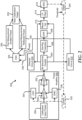
- FIG. 2 illustrates circuitry 200 to perform output power calibration in accordance with an embodiment of the current disclosure.
- Circuitry 200 includes a PA 202, a bi-directional coupler 204, a die/package transition 206, an antenna reference plane (ARP) 208, and detector circuits 210 and 212.
- Circuitry 200 further includes a mixer circuit 214, a low pass (LP) filter 216, and analog-to-digital (ADC) converter 218, a digital comparator 220, a control circuit 222, and a voltage gain amplifier (VGA) 224.
- PA 202 includes a driver 230, an output 232, a load dropout (LDO) circuit 234, and a current digital-to-analog circuit (iDAC) 236.
- LDO load dropout
- iDAC current digital-to-analog circuit
- Circuitry 200 may include additional components without varying from the scope of this disclosure.
- PA 202 may provide a signal to through bi-directional coupler 204 and die/package transition 206 to ARP 208. As the signal is provided through these components, a reflected signal may be sent back from ARP 208 toward PA 202.
- Bi-directional coupler 204 may separate the incident, or originally transmitted, signal from the reflected signal. Bi-directional coupler 204 may provide the incident signal to detector circuit 210, and provide the reflected signal to detector 212.
- detector circuit 210 may be a PPD circuit and may be coupled to the output of PA 202. Detector circuit 210 may detect or determine the amplitude of the output signal from PA 202.
- Detector circuit 212 may be a PPD circuit and may be isolated from the output of PA 202. Detector circuit 212 may detect or determine the amplitude of the reflected signal.
- Detector circuits 210 and 212 may be coupled to VGA 224 through respective switches 240 and 242 in the communication paths between the detector circuits and the VGA.
- One of the switches 240 and 242 may be closed while the other switch is open, such that only one of the determined amplitudes is provided to VGA 224 at a time.
- switch 240 may be closed and switch 242 may be open, such that VGA 224 may measure incident power 250.
- switch 240 may be open and switch 242 may be closed, such that VGA may measure reflected power 252.
- a new calibration target 254 may be calculated for PA 202.
- the calibration target 254 may be calculated based on a previous calibration target being added to the output voltage from detector circuit 212.
- the new calibration target 254 may be utilized as a calibrated input power 260 provided to driver 230 of PA 202.
- Bi-directional coupler 204 may provide the incident signal and the reflected signal to the mixer circuit 214.
- mixer circuit 214 may determine a phase difference between the two signals. Different embodiments of mixer circuit 214 will be described with respect to FIGs. 3-9 below. Based on the determined phase difference, mixer circuit 214 may determine a standing wave signal (SWS) amplitude at the output of PA 202. Based on the comparison, digital comparator 220 may provide a calibration mode signal to control circuit 222. For example, the calibration mode signal may indicate whether to increase voltage, increase current, or both of PA 202 to compensate for the impedance mismatch.
- the threshold value may be any suitable value, such as a safe operating area (SOA) value for PA 202. The comparison to a SOA threshold may ensure that the SOA threshold is not exceeded while still compensating for the power impedance mismatch.
- SOA safe operating area
- control circuit 222 may determine whether to increase voltage, increase current, or both of PA 202 to compensate for the impedance mismatch. If control circuit 222 determines that the voltage should be increased, the control circuit may provide a control signal to LDO 234, which in turn may increase the supply voltage to driver 230 and output 232 of PA 202. If control circuit 222 determines that the current should be increased, the control circuit may provide a control signal to iDAC 236, which in turn may increase the bias current to driver 230 and output 232 of PA 202. Additionally, if control circuit 222 determines that both the voltage and the current should be increased, the control circuit may provide a control signal to both LDO 234 and iDAC 236. In response to the control signal, LDO 234 may increase the supply voltage to driver 230 and output 232 of PA 202 and iDAC 236 may increase the bias current to the driver and the output.
- FIG. 3 illustrates mixer calibration circuitry 300 in accordance with an embodiment of the current disclosure.
- Mixer calibration circuitry 300 may be substantially similar to mixer circuit 214 of FIG. 2 .
- Mixer calibration circuitry 300 includes a mixer 302, input terminals 304 and 306, and an output terminal 308.
- the incident signal as described above with respect to FIG. 2
- the reflected signal as also described above with respect to FIG. 2
- input terminal 304 may be coupled to the LO input of mixer 302.
- the amplitude of the incident signal may be selected in a manner that does not affect a gain of the mixer.
- Mixer 302 may operate as a phase detector to determine a phase difference between the incident signal and the reflected signal.
- the mixer may provide an output voltage signal at output terminal 308.
- both ⁇ _ofst and ⁇ ofst may be values determined in a lab, and may represent correction values that may be independent on a process, voltage, and temperature (PVT) for the particular PCB.
- a max may be calculated based upon A 2 and a gain of mixer 302.
- the gain of mixer 302 may be determined or trimmed in any suitable manner.
- the gain of mixer 302 may be trimmed by sweeping a gamma phase at the output of a transmitter, such as transmitter 122 of FIG. 1 , to determine a correction factor.
- the sweeping of the gamma phase may generate a reflection coefficient of a matching ratio between the incident and reflected signals, and a Fast Fourier Transform (FFT) may be performed on the reflection coefficient to determine the correction factor.
- the correction factor may be loaded within digital circuit 220 during a start up sequence of the PCB.
- ⁇ 2 - ⁇ 1 may be calculated, which is the phase of the reflected signal minus the phase of the incident signal. This difference may be referred to as the phase difference between the signals and this phase difference is utilized to correct an impedance mismatch as described above with respect to FIG. 2 .
- FIG. 4 illustrates mixer gain trimmer circuitry 400 in accordance with an embodiment of the current disclosure.
- Mixer gain trimmer circuitry 400 includes a bi-directional coupler 402, detector circuits 404 and 406, mixer circuitry 408, and a LP filter 410.
- Bi-directional coupler 402 may be substantially similar to bi-directional coupler 204 of FIG. 2
- detector circuits 404 and 406 may be substantially similar to respective detector circuits 210 and 212 of FIG. 2
- LP filter 410 may be substantially similar to LP filter 216 of FIG. 2 .
- Bi-directional coupler 402 may receive an output signal from a PA, such as PA 202 of FIG. 2 , and may determine an incident signal the output, and may receive a reflection from a load, such as ARP 208 of FIG. 2 , and may determine a reflected signal from the reflection. Bi- directional coupler 402 may provide the incident signal to detector circuit 404 and the reflected signal to detector circuit 406. Detector circuit 404 may determine an amplitude, A1, for the incident signal, and detector circuit 406 may determine an amplitude, A2, for the reflected signal. These amplitudes may be utilized in determining a gain of mixer circuit 408 as will be described below.
- the measurement/characterization of the gain of mixer 408 may be performed by a gamma phase at the load being swept between 0 and 359 degrees. As the phase is swept between 0 and 359 degrees, a complete sinusoid may be generated at the output of LP filter 410 by measuring Vout for each gamma phase.
- a Vout max and a Vout min may be determined for the sinusoid across the phase sweep.
- a max , ⁇ ofst , and other variables may be determined based on a FFT of the output from LP filter 410.
- ⁇ ofst may be equivalent to the initial phase of the sinusoid
- a max may be the amplitude of the fundamental
- ⁇ 2 - ⁇ 1 may be the frequency of the fundamental.
- FIG. 5 illustrates a flow diagram of a method for recalibrating an output power of a power amplifier in accordance with an embodiment of the current disclosure, starting at block 502.
- the method may be performed by any suitable component including, but not limited to, components in circuitry 200 of FIG. 2 , or any other suitable component. Not every method step set forth in this flow diagram is always necessary, and certain steps of the methods may be combined, performed simultaneously, in a different order, or perhaps omitted, without varying from the scope of the disclosure.
- trimming data for a mixer is received.
- the trimming data may be stored in a memory of a digital circuit of a PCB, such as digital circuit 220 in FIG. 1 of PCB 102 of FIG. 1 , and the trimming data may be utilized to determine a maximum amplitude, Amax, for an output voltage.
- a 2 is the amplitude of a reflected signal of a power amplifier, such as PA 202 of FIG. 2 .
- the output voltage of the PA is calibrated.
- the output voltage may be calibrated in any suitable manner.
- an amplitude of an output voltage from a coupled detector circuit may be utilized to calibrate the PA.
- the coupled detector circuit may determine the amplitude of an incident signal from the PA.
- an output voltage from an isolated detector circuit is measured.
- the output voltage from the isolated detector circuit may be an amplitude of a reflected signal in a transmission path from the PA to an antenna.
- the reflected signal may be created based on an impedance mismatch between the transmitter and the antenna.
- a direct current (DC) voltage of the mixer circuit is measured.
- a phase difference between the incident signal and the reflected signal is determined.
- the phase difference may be determined or calculated in any suitable manner.
- Amax and ⁇ ofst may be calculated as described above with respect to FIG. 4 .
- a calibration target for the PA is updated.
- the calibration target may be updated in any suitable manner utilizing any suitable values in transmission circuitry.
- an amplitude of a standing wave signal is calculated.
- the amplitude of the SWS may be calculated based on the amplitude of the incident signal, the amplitude of the reflected signal, and a phase difference between the incident and reflected signals.
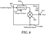
- FIG. 6 illustrates mixer calibration circuitry 600 in accordance with an embodiment of the current disclosure.
- Mixer calibration circuitry 600 may be substantially similar to mixer circuit 214 of FIG. 2 .
- Mixer calibration circuitry 600 includes a mixer 602, a phase control circuit 604, input terminals 606 and 608, and an output terminal 610.
- the incident signal as described above with respect to FIG. 2 , may be received at input terminal 606, and the reflected signal, as also described above with respect to FIG. 2 , may be received at input terminal 608.
- Input terminal 606 may be coupled to phase control circuit 604, which in turn is coupled to a LO input of mixer 602.
- the amplitude of the incident signal may be selected in a manner that does not affect a gain of the mixer.
- Mixer 602 may operate as a phase detector to determine a phase difference between the incident signal and the reflected signal.
- Phase shift circuit 604 includes a control input terminal 612 to receive a control signal. In certain examples, the control signal may cause phase shift circuit 604 to either not introduce a phase shift, such as 0 degree shift, or introduce a phase shift, such as a 90 degree phase shift.
- the mixer may provide a first output voltage signal at output terminal 610.
- the mixer may provide a second output voltage signal at output terminal 610.
- ⁇ 2 - ⁇ 1 may be calculated, which is the phase of the reflected signal minus the phase of the incident signal. This difference may be referred to as the phase difference between the signals and this phase difference is utilized to correct an impedance mismatch as described above with respect to FIG. 2 .
- FIG. 7 illustrates a flow diagram of a method for recalibrating an output power of a power amplifier in accordance with another embodiment of the current disclosure, starting at block 702.
- the method may be performed by any suitable component including, but not limited to, components in circuitry 200 of FIG. 2 , or any other suitable component. Not every method step set forth in this flow diagram is always necessary, and certain steps of the methods may be combined, performed simultaneously, in a different order, or perhaps omitted, without varying from the scope of the disclosure.
- the output voltage of the PA is calibrated.
- the output voltage may be calibrated in any suitable manner.
- an amplitude of an output voltage from a coupled detector circuit may be utilized to calibrate the PA.
- the coupled detector circuit may determine the amplitude of an incident signal from the PA.
- an output voltage from an isolated detector circuit is measured.
- the output voltage from the isolated detector circuit may be an amplitude of a reflected signal in a transmission path from the PA to an antenna.
- the reflected signal may be created based on an impedance mismatch between the transmitter and the antenna.
- a direct current (DC) voltage of a mixer circuit is measured at a 0 degree phase control of an incident signal.
- a direct current (DC) voltage of a mixer circuit is measured at a 90 degree phase control of an incident signal.
- a maximum amplitude, A max of an output voltage from the mixer circuit is determined.
- a phase difference between the incident signal and the reflected signal is determined.
- the phase difference may be determined or calculated in any suitable manner.
- a max and ⁇ ofst may be calculated as described above with respect to FIG. 4 .
- a calibration target for the PA is updated.
- the calibration target may be updated in any suitable manner utilizing any suitable values in transmission circuitry.
- an amplitude of a SWS is calculated.
- the amplitude of the SWS may be calculated based on the amplitude of the incident signal, the amplitude of the reflected signal, and a phase difference between the incident and reflected signals.
- FIG. 8 illustrates mixer calibration circuitry 800 in accordance with an embodiment of the current disclosure.
- Mixer calibration circuitry 800 may be substantially similar to mixer circuit 214 of FIG. 2 .
- Mixer calibration circuitry 800 includes mixers 802 and 804, phase shift circuits 806 and 808, input terminals 810 and 812, and output terminals 814 and 806.
- the incident signal as described above with respect to FIG. 2
- the reflected signal as also described above with respect to FIG. 2
- input terminal 810 may be coupled to both phase shift circuits 806 and 808.
- Mixers 802 and 804 may operate as phase detectors to determine a phase difference between the incident signal and the reflected signal.
- the incident signal output from phase shift circuit 806 may be provided to mixer 802.
- the incident signal output from phase shift circuit 808 may be provided to mixer 804.
- the reflected signal may be provided to both mixers 802 and 804.
- Mixer 802 may provide an output voltage signal at output terminal 814.
- Mixer 804 may provide an output voltage signal at output terminal 816.
- a max may be calculated based upon the two voltage outputs, such as V out 0 and Vout 90 .
- a max may be determined without consideration of trimming data for the mixer.
- ⁇ diff may be calculated, which is the phase of the reflected signal minus the phase of the incident signal. This difference may be referred to as the phase difference between the signals and this phase difference is utilized to correct an impedance mismatch as described above with respect to FIG. 2 .
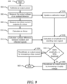
- FIG. 9 illustrates a flow diagram of a method 900 for recalibrating an output power of a power amplifier in accordance with an embodiment of the current disclosure, starting at block 902.
- the method may be performed by any suitable component including, but not limited to, components in circuitry 200 of FIG. 2 , or any other suitable component. Not every method step set forth in this flow diagram is always necessary, and certain steps of the methods may be combined, performed simultaneously, in a different order, or perhaps omitted, without varying from the scope of the disclosure.
- the output voltage of the PA is calibrated.
- the output voltage may be calibrated in any suitable manner.
- an amplitude of an output voltage from a coupled detector circuit may be utilized to calibrate the PA.
- the coupled detector circuit may determine the amplitude of an incident signal from the PA.
- an output voltage from an isolated detector circuit is measured.
- the output voltage from the isolated detector circuit may be an amplitude of a reflected signal in a transmission path from the PA to an antenna.
- the reflected signal may be created based on an impedance mismatch between the transmitter and the antenna.
- two DC voltages of a mixer circuit is measured.
- the two DC voltages may be output from the mixer circuitry at substantially the same time.
- One of the DC voltages is measured at a 0 degree phase control of an incident signal, and the other DC voltage is measured at a 90 degree phase control of the incident signal.
- a maximum amplitude, A max of an output voltage from the mixer circuit is determined.
- a phase difference between the incident signal and the reflected signal is determined.
- the reflected signal may be determined or calculated in any suitable manner.
- a max and ⁇ ofst may be calculated as described above with respect to FIG. 4 .
- a calibration target for the PA is updated.
- the calibration target may be updated in any suitable manner utilizing any suitable values in transmission circuitry.
- an amplitude of a SWS is calculated.
- the amplitude of the SWS may be calculated based on the amplitude of the incident signal, the amplitude of the reflected signal, and a phase difference between the incident and reflected signals.
Landscapes
- Engineering & Computer Science (AREA)
- Radar, Positioning & Navigation (AREA)
- Remote Sensing (AREA)
- Power Engineering (AREA)
- Computer Networks & Wireless Communication (AREA)
- Physics & Mathematics (AREA)
- General Physics & Mathematics (AREA)
- Amplifiers (AREA)
Abstract
A transmitter circuit includes a power amplifier and a mixer calibration circuit. The power amplifier provides a transmission signal. The mixer calibration circuit receives an incident signal of the transmission signal and a reflected signal of the transmission signal. Based on an amplitude of the reflected signal and on a phase difference between the incident and reflected signals, the mixer calibration circuit determines an amplitude of a standing wave signal. Based on the amplitude of the standing wave signal, the mixer calibration circuit causes a recalibration of an output voltage and the bias current of the power amplifier
Description
- This disclosure generally relates to the fabrication of semiconductor devices, and more particularly relates to radar transmitter output power calibration via a standing wave signal detector and a calibration apparatus.
- A radar transmitter includes multiple components including a power amplifier (PA), an antenna, and an antenna reference plane. In certain situations, an impedance mismatch may occur between the output of the PA and the antenna reference plane. In previous radar transmitters, radar transmitter output power calibration was utilized to compensate for a power loss due to this mismatch. Although the output power calibration may solve the mismatch issue, the calibration may cause the devices of the PA to enter an undesired operating area during particular conditions. For example, when the radar transmitter has very high output power and very high mismatch conditions, the devices of the PA may enter the undesired operating area. The undesired operating area may cause stress on components of the PA. In particular, the mismatch conditions may be corrected but a voltage swing at an output of the PA may exceed a safe operating area. The components of the PA may be damaged by the output voltage exceeding the safe operating area.
- Radar transmitter may be improved by ensuring safe power control for the transmitter. However, this requires a breakthrough in the transmitter to find a new approach to ensure that the voltage standing wave signal will not exceed the safe operating area threshold once the mismatch is compensated.
- It will be appreciated that for simplicity and clarity of illustration, elements illustrated in the Figures have not necessarily been drawn to scale. For example, the dimensions of some of the elements are exaggerated relative to other elements. Embodiments incorporating teachings of the present disclosure are shown and described with respect to the drawings presented herein, in which:
-
FIG. 1 illustrates a printed circuit board having a power amplifier and an antenna in accordance with an embodiment of the current disclosure; -
FIG. 2 illustrates a block diagram of circuitry to perform output power calibration in accordance with an embodiment of the current disclosure; -
FIG. 3 illustrates a block diagram of a mixer calibration circuitry in accordance with an embodiment of the current disclosure; -
FIG. 4 illustrates a block diagram of a mixer gain trimmer circuitry in accordance with an embodiment of the current disclosure; -
FIG. 5 illustrates a flow diagram of a method for recalibrating an output power of a power amplifier in accordance with an embodiment of the current disclosure; -
FIG. 6 illustrates a block diagram of a mixer calibration circuitry in accordance with another embodiment of the current disclosure; -
FIG. 7 illustrates a flow diagram of a method for recalibrating an output power of a power amplifier in accordance with another embodiment of the current disclosure; -
FIG. 8 illustrates a block diagram of a mixer calibration circuitry in accordance with another embodiment of the current disclosure; and -
FIG. 9 illustrates a flow diagram of a method for recalibrating an output power of a power amplifier in accordance with another embodiment of the current disclosure. - The use of the same reference symbols in different drawings indicates similar or identical items.
- A transmitter circuit includes a power amplifier and a mixer calibration circuit. The power amplifier may provide a transmission signal. The mixer calibration circuit may communicate with the power amplifier. The mixer calibration circuit may receive an incident signal of the transmission signal and a reflected signal of the transmission signal. Based on an amplitude of the reflected signal and on a phase difference between the incident and reflected signals, the mixer calibration circuit may determine an amplitude of a standing wave signal. Based on the amplitude of the standing wave signal, the mixer calibration circuit may cause recalibration of an output voltage and the bias current of the power amplifier.
- The following description in combination with the Figures is provided to assist in understanding the teachings disclosed herein. The description will focus on specific implementations and embodiments of the teachings. This focus is provided to assist in describing the teachings, and should not be interpreted as a limitation on the scope or applicability of the teachings. Moreover, other teachings can be used in association with the teachings of this application, as needed or desired, without limiting the scope of the teachings herein.
- In an embodiment of the current disclosure, a transmitter circuit may include a power amplifier and a mixer calibration circuit. The power amplifier may provide a transmission signal. The mixer calibration circuit may communicate with the power amplifier. The mixer calibration circuit may receive an incident signal of the transmission signal and a reflected signal of the transmission signal. Based on an amplitude of the reflected signal, a prior measurement/characterization of the mixer gain, and on a phase difference between the incident and reflected signals, the mixer calibration circuit may determine an amplitude of a standing wave signal. Based on the amplitude of the standing wave signal, the mixer calibration circuit may cause recalibration of an output voltage of the power amplifier.
- In an embodiment, the transmitter circuit may also include a comparator coupled to the mixer calibration circuit. The comparator may compare the amplitude of the standing wave signal with a threshold value, and output a calibration mode signal. The transmitter may further include a control circuit coupled to the comparator. The control circuit may receive the calibration mode signal. In response to the calibration mode signal indicating a first calibration mode, the control circuit may increase a bias current to a driver of the power amplifier. In an embodiment, the increase of the bias current recalibrates the output voltage of the power amplifier. In response to the calibration mode signal indicating a second calibration mode, the control circuit may increase a supply voltage to the driver of the power amplifier. In an embodiment, the increase of the bias current recalibrates the output voltage of the power amplifier.
- In an embodiment, the first calibration mode may be based on the amplitude of the standing wave signal being greater than the threshold value, and the second calibration mode is based on the amplitude of the standing wave signal being less than the threshold value. In response to the calibration mode signal indicating the second calibration mode, the control circuit may increase the bias current to the driver of the power amplifier.
- In an embodiment, the mixer calibration circuit may include a phase control circuit and a mixer. The phase control circuit may receive the incident signal. Based on a first phase control signal, the phase control circuit may provide the incident signal with a zero degree phase shift. Based on a second phase control signal, the phase control circuit may provide the incident signal with a ninety degree phase shift. The mixer may be coupled to the phase control circuit. The mixer may receive the reflected signal, and receive the incident signal from the phase control circuit. Based on the incident signal having the zero degree phase shift, the mixer may provide a first output voltage. Based on the incident signal having the ninety degree phase shift, the mixer may provide a second output voltage, wherein the amplitude of the standing wave is calculated based on the first and second output voltages and on a phase difference between the incident and reflected signals.
- In another embodiment, the mixer calibration circuit may include first and second phase control circuits, and first and second mixers. The first phase control circuit may receive the incident signal, and provide the incident signal with a zero degree phase shift. The second phase control circuit may receive the incident signal, and provide the incident signal with a ninety degree phase shift. The first mixer may be coupled to the first phase control circuit. The first mixer may receive the reflected signal, and receive the incident signal with the zero degree phase shift from the first phase control circuit. Based on the incident signal having the zero degree phase shift, the first mixer may provide a first output voltage. The second mixer may be coupled to the second phase control circuit. The second mixer may receive the reflected signal, and receive the incident signal with the ninety degree phase shift from the second phase control circuit. Based on the incident signal having the ninety degree phase shift, the second mixer may
provide a second output voltage. The amplitude of the standing wave may be calculated based on the first and second output voltages and on a phase difference between the incident and reflected signals. - In an embodiment, the transmitter circuit may further include a bi-directional coupler coupled to the power amplifier. The bi-directional coupler may provide the incident signal and the reflected signal to the mixer calibration circuit.
- In another embodiment of the current disclosure, a method of re-calibrating a power amplifier is given. The method may include providing, by a power amplifier of a transmitter circuit, a transmission signal. The method may further include receiving, by a mixer calibration circuit of the transmitter circuit, an incident signal of the transmission signal and a reflected signal of the transmission signal. Based on an amplitude of the reflected signal and on a phase difference between the incident and reflected signals, the method may also include determining an amplitude of a standing wave signal. Based on the amplitude of the standing wave signal, the method may further include recalibrating an output voltage of the power amplifier.
- In an embodiment, the method may further include comparing, by a comparator of the transmitter circuit, the amplitude of the standing wave signal with a threshold value. The method may also include outputting, by the comparator, a calibration mode signal.
- In an embodiment, the method may further include receiving, by a control circuit of the transmitter circuit, the calibration mode signal. In response to the calibration mode signal indicating a first calibration mode, the method may also include increasing, by the control circuit, a bias current to a driver of the power amplifier. The increase of the bias current recalibrates the output voltage of the power amplifier. In response to the calibration mode signal indicating a second calibration mode, the method may further include increasing, by the control circuit, a supply voltage to the driver of the power amplifier. The increase of the bias current recalibrates the output voltage of the power amplifier.
- In an embodiment, the first calibration mode is based on the amplitude of the standing wave signal being greater than the threshold value. The second calibration mode is based on the amplitude of the standing wave signal being less than the threshold value. In response to the
calibration mode signal indicating the second calibration mode, the control circuit may further increase the bias current to the driver of the power amplifier. - In an embodiment, the method may further include receiving, by a phase control circuit of the mixer calibration circuit, the incident signal. Based on a first phase control signal, the method may also include providing the incident signal with a zero degree phase shift. Based on a second phase control signal, the method may further include providing the incident signal with a ninety degree phase shift. The method may also include receiving, by a mixer of the mixer calibration circuit, the reflected signal, and receiving the incident signal from the phase control circuit. Based on the incident signal having the zero degree phase shift, the method may further include providing a first output voltage of the mixer. Based on the incident signal having the ninety degree phase shift, the method may also include providing a second output voltage of the mixer. The amplitude of the standing wave is calculated based on the first and second output voltages and on a phase difference between the incident and reflected signals.
- In an embodiment, the method may further include receiving, by a first phase control circuit of the mixer calibration circuit, the incident signal. The method may also include providing, by the first phase control circuit, the incident signal with a zero degree phase shift. The method may further include receiving, by a second phase control circuit of the mixer calibration circuit, the incident signal. The method may also include providing, by the second phase control circuit, the incident signal with a ninety degree phase shift. The method may further include receiving, by a first mixer of the mixer calibration circuit, the reflected signal. The method may also include receiving, by the first mixer, the incident signal with the zero degree phase shift from the first phase control circuit. Based on the incident signal having the zero degree phase shift, the method may further include providing a first output voltage. The method may also include receiving, by a second mixer of the mixer calibration circuit, the reflected signal. The method may further include receiving, by the second mixer the incident signal with the ninety degree phase shift from the second phase control circuit. Based on the incident signal having the ninety degree phase shift, the method may also include providing a second output voltage. The amplitude of the standing wave is calculated based on the first and second output voltages and on a phase difference between the incident and reflected signals.
- In yet another embodiment of the current disclosure, a transmitter circuit includes a power amplifier, a bi-directional coupler, a mixer calibration circuit, a comparator, and a control circuit. The power amplifier may provide a transmission signal. The bi-directional coupler may be coupled to the power amplifier, and provide an incident signal of the transmission signal and a reflected signal of the transmission signal. The mixer calibration circuit may be coupled to the
bi-directional coupler. The mixer calibration circuit may receive the incident signal and the reflected signal. Based on an amplitude of the reflected signal and on a phase difference between the incident and reflected signals, the mixer calibration circuit may determine an amplitude of a standing wave signal. Based on the amplitude of the standing wave signal, the mixer calibration circuit may cause recalibration of an output voltage of the power amplifier. The comparator may be coupled to the mixer calibration circuit. The comparator may compare the amplitude of the standing wave signal with a threshold value, and output a calibration mode signal. The control circuit may be coupled to the comparator. The control circuit may receive the calibration mode signal. In response to the calibration mode signal indicating a first calibration mode, the control circuit may increase a bias current to a driver of the power amplifier. The increase of the bias current recalibrates the output voltage of the power amplifier. In response to the calibration mode signal indicating a second calibration mode, the control circuit may increase a supply voltage to the driver of the power amplifier. The increase of the bias current recalibrates the output voltage of the power amplifier. - The first calibration mode may be based on the amplitude of the standing wave signal being greater than the threshold value. The second calibration mode may be based on the amplitude of the standing wave signal being less than the threshold value.
-
FIG. 1 illustrates a printed circuit board (PCB) 102 havingpackage 104 and one ormore antennas 106 in accordance with an embodiment of the current disclosure.Package 104 includes an integrated circuit (IC) 110.IC 110 includes a transmit power amplifier (PA) 120, atransmitter 122,detector circuits mixer 128, and alow pass filter 130.Detector circuits PCB 102 may include additional components without varying from the scope of this disclosure. -
PCB 102 may include a PA output impedance Z 1, a transmitter impedance Z2, a transmitter output impedance Z3, and an antenna input impedance Z4 along a transmission path fromPA 120 toantennas 106. When an ideal calibration condition exists withinPCB 102, PA output impedance Z1 is matched to transmitter input impedance Z2, and transmitter output impedance Z3 is matched to antenna input impedance Z4. However, actual calibration conditions may be different such that transmitter input impedance Z2 and antenna input impedance Z4 vary compared to the respective initial calibration matched conditions. For example, actual conditions may cause the actual transmitter input impedance to equal Z2+deltaZ2 and the actual antenna input impedance to equal Z4+deltaZ4. -
Detector circuits mixer 128, andlow pas filter 130 may combine to improve the calibration of the output fromPA 120.Detector circuit 124 may detect a reflected signal fromPA 120 anddetector circuit 126 may detect an incident signal fromPA 120. The detected signals may be provided fromdetector circuits mixer circuit 128. In response to receiving the detected signals,mixer circuit 128 may determine a phase difference between the reflected and incident output voltages. Based on the phase difference,LP 130 may be utilized to determine a voltage swing at the output ofPA 120. The voltage swing and phase difference may be utilized during a recalibration as will be described with respect toFIGs. 2-9 below. The recalibration may preventPA 120 from entering an undesired operating area that may cause stress on components of the PA. In particular, the recalibration as will be described with respect toFIGs. 2-9 below may correct the mismatch conditions and hold a voltage swing at an output ofPA 120 within a safe operating area. Maintaining the voltage within the safe operating area may prevent the components ofPA 120 from being damaged. -
FIG. 2 illustratescircuitry 200 to perform output power calibration in accordance with an embodiment of the current disclosure.Circuitry 200 includes aPA 202, abi-directional coupler 204, a die/package transition 206, an antenna reference plane (ARP) 208, anddetector circuits Circuitry 200 further includes amixer circuit 214, a low pass (LP)filter 216, and analog-to-digital (ADC)converter 218, adigital comparator 220, acontrol circuit 222, and a voltage gain amplifier (VGA) 224.PA 202 includes a driver 230, anoutput 232, a load dropout (LDO)circuit 234, and a current digital-to-analog circuit (iDAC) 236. The functions and features ofPA 202,bi-directional coupler 204, die/package transition 206, andARP 208 are known in the art and will not be further disclosed herein, except as needed to illustrate the various embodiments disclosed herein.Circuitry 200 may include additional components without varying from the scope of this disclosure. -
PA 202 may provide a signal to throughbi-directional coupler 204 and die/package transition 206 toARP 208. As the signal is provided through these components, a reflected signal may be sent back fromARP 208 towardPA 202.Bi-directional coupler 204 may separate the incident, or originally transmitted, signal from the reflected signal.Bi-directional coupler 204 may provide the incident signal todetector circuit 210, and provide the reflected signal todetector 212. In certain examples,detector circuit 210 may be a PPD circuit and may be coupled to the output ofPA 202.Detector circuit 210 may detect or determine the amplitude of the output signal fromPA 202.Detector circuit 212 may be a PPD circuit and may be isolated from the output ofPA 202.Detector circuit 212 may detect or determine the amplitude of the reflected signal. -
Detector circuits VGA 224 throughrespective switches switches VGA 224 at a time. For example, switch 240 may be closed and switch 242 may be open, such thatVGA 224 may measureincident power 250. Next, switch 240 may be open and switch 242 may be closed, such that VGA may measurereflected power 252. Based onmeasure incident power 250 and measured reflectedpower 252, anew calibration target 254 may be calculated forPA 202. In an example, thecalibration target 254 may be calculated based on a previous calibration target being added to the output voltage fromdetector circuit 212. Thenew calibration target 254 may be utilized as a calibratedinput power 260 provided to driver 230 ofPA 202. -
Bi-directional coupler 204 may provide the incident signal and the reflected signal to themixer circuit 214. In response to receiving the incident and reflected signals,mixer circuit 214 may determine a phase difference between the two signals. Different embodiments ofmixer circuit 214 will be described with respect toFIGs. 3-9 below. Based on the determined phase difference,mixer circuit 214 may determine a standing wave signal (SWS) amplitude at the output ofPA 202. Based on the comparison,digital comparator 220 may provide a calibration mode signal to controlcircuit 222. For example, the calibration mode signal may indicate whether to increase voltage, increase current, or both ofPA 202 to compensate for the impedance mismatch. In an example, the threshold value may be any suitable value, such as a safe operating area (SOA) value forPA 202. The comparison to a SOA threshold may ensure that the SOA threshold is not exceeded while still compensating for the power impedance mismatch. - Based on the calibration mode signal,
control circuit 222 may determine whether to increase voltage, increase current, or both ofPA 202 to compensate for the impedance mismatch. Ifcontrol circuit 222 determines that the voltage should be increased, the control circuit may provide a control signal toLDO 234, which in turn may increase the supply voltage to driver 230 andoutput 232 ofPA 202. Ifcontrol circuit 222 determines that the current should be increased, the control circuit may provide a control signal toiDAC 236, which in turn may increase the bias current to driver 230 andoutput 232 ofPA 202. Additionally, ifcontrol circuit 222 determines that both the voltage and the current should be increased, the control circuit may provide a control signal to bothLDO 234 andiDAC 236. In response to the control signal,LDO 234 may increase the supply voltage to driver 230 andoutput 232 ofPA 202 andiDAC 236 may increase the bias current to the driver and the output. -
FIG. 3 illustratesmixer calibration circuitry 300 in accordance with an embodiment of the current disclosure.Mixer calibration circuitry 300 may be substantially similar tomixer circuit 214 ofFIG. 2 .Mixer calibration circuitry 300 includes amixer 302,input terminals output terminal 308. In an example, the incident signal, as described above with respect toFIG. 2 , may be received atinput terminal 304, and the reflected signal, as also described above with respect toFIG. 2 , may be received atinput terminal 306. In certain examples,input terminal 304 may be coupled to the LO input ofmixer 302. Based on the incident signal being received atinput terminal 304 and the LO input ofmixer 302, the amplitude of the incident signal may be selected in a manner that does not affect a gain of the mixer.Mixer 302 may operate as a phase detector to determine a phase difference between the incident signal and the reflected signal. - The incident signal may be represented by Vrf 1 = A1 ∗cos(wt + Φ1), where A1 is the amplitude of the incident signal measured by
detector circuit 210 ofFIG. 2 , and Φ1 is the phase of the incident signal. The reflected signal received atinput terminal 306 may be represented by Vrf 2 = A2 ∗cos(wt + Φ2), where A2 is the amplitude of the reflected signal measured bydetector circuit 212 ofFIG. 2 , and Φ2 is the phase of the reflected signal. Based on the incident signal and the reflected signal being received atmixer 302, the mixer may provide an output voltage signal atoutput terminal 308. In an example, the output voltage signal may be represented by V out = Amax ∗cos(Φ2 - Φ1 + Φofst) + A_ofst, where Φ_ofst may be an offset amplitude and Φofst may be an offset phase. In certain examples, both Φ_ofst and Φofst may be values determined in a lab, and may represent correction values that may be independent on a process, voltage, and temperature (PVT) for the particular PCB. - Amax may be calculated based upon A2 and a gain of
mixer 302. The gain ofmixer 302 may be determined or trimmed in any suitable manner. For example, the gain ofmixer 302 may be trimmed by sweeping a gamma phase at the output of a transmitter, such astransmitter 122 ofFIG. 1 , to determine a correction factor. The sweeping of the gamma phase may generate a reflection coefficient of a matching ratio between the incident and reflected signals, and a Fast Fourier Transform (FFT) may be performed on the reflection coefficient to determine the correction factor. The correction factor may be loaded withindigital circuit 220 during a start up sequence of the PCB. - Based on the equations above, Φ2 - Φ1 may be calculated, which is the phase of the reflected signal minus the phase of the incident signal. This difference may be referred to as the phase difference between the signals and this phase difference is utilized to correct an impedance mismatch as described above with respect to
FIG. 2 . -
FIG. 4 illustrates mixer gaintrimmer circuitry 400 in accordance with an embodiment of the current disclosure. Mixergain trimmer circuitry 400 includes abi-directional coupler 402,detector circuits mixer circuitry 408, and aLP filter 410.Bi-directional coupler 402 may be substantially similar tobi-directional coupler 204 ofFIG. 2 ,detector circuits respective detector circuits FIG. 2 , andLP filter 410 may be substantially similar toLP filter 216 ofFIG. 2 . -
Bi-directional coupler 402 may receive an output signal from a PA, such asPA 202 ofFIG. 2 , and may determine an incident signal the output, and may receive a reflection from a load, such asARP 208 ofFIG. 2 , and may determine a reflected signal from the reflection. Bi-directional coupler 402 may provide the incident signal todetector circuit 404 and the reflected signal todetector circuit 406.Detector circuit 404 may determine an amplitude, A1, for the incident signal, anddetector circuit 406 may determine an amplitude, A2, for the reflected signal. These amplitudes may be utilized in determining a gain ofmixer circuit 408 as will be described below. - The measurement/characterization of the gain of
mixer 408 may be performed by a gamma phase at the load being swept between 0 and 359 degrees. As the phase is swept between 0 and 359 degrees, a complete sinusoid may be generated at the output ofLP filter 410 by measuring Vout for each gamma phase. The sinusoid at the output ofLP filter 410 may be represented by V out = Amax ∗cos(Φ2 - Φ1 + Φofst) + A_ofst. A Voutmax and a Voutmin may be determined for the sinusoid across the phase sweep. A_ofst may be determined as: A_ ofst = (Voutmax - Voutmin)/2. Amax, Φofst, and other variables may be determined based on a FFT of the output fromLP filter 410. For example, Φofst may be equivalent to the initial phase of the sinusoid, Amax may be the amplitude of the fundamental, and Φ2 - Φ1 may be the frequency of the fundamental. Additionally, the value A2 may be measured from theisolated detector circuit 406. Based on these calculations, the gain ofmixer 408 may be substantially equal to: mixergain = Amax/A2 . After the gain ofmixer 408 has been calculated, the value of the gain may be stored in a memory of digital circuit of a PCB, such asdigital circuit 220 inFIG. 1 ofPCB 102 ofFIG. 1 . -
FIG. 5 illustrates a flow diagram of a method for recalibrating an output power of a power amplifier in accordance with an embodiment of the current disclosure, starting at block
502. In an example, the method may be performed by any suitable component including, but not limited to, components incircuitry 200 ofFIG. 2 , or any other suitable component. Not every method step set forth in this flow diagram is always necessary, and certain steps of the methods may be combined, performed simultaneously, in a different order, or perhaps omitted, without varying from the scope of the disclosure. - At
block 504, trimming data for a mixer is received. The trimming data may be stored in a memory of a digital circuit of a PCB, such asdigital circuit 220 inFIG. 1 ofPCB 102 ofFIG. 1 , and the trimming data may be utilized to determine a maximum amplitude, Amax, for an output voltage. For example, the trimming data may include a gain of a mixer circuit, and Amax = mixergain ∗ A2. In this example, A2 is the amplitude of a reflected signal of a power amplifier, such asPA 202 ofFIG. 2 . - At
block 506, the output voltage of the PA is calibrated. The output voltage may be calibrated in any suitable manner. For example, an amplitude of an output voltage from a coupled detector circuit may be utilized to calibrate the PA. The coupled detector circuit may determine the amplitude of an incident signal from the PA. - At
block 508, an output voltage from an isolated detector circuit is measured. The output voltage from the isolated detector circuit may be an amplitude of a reflected signal in a transmission path from the PA to an antenna. The reflected signal may be created based on an impedance mismatch between the transmitter and the antenna. - At
block 510, a direct current (DC) voltage of the mixer circuit is measured. Atblock 512, a phase difference between the incident signal and the reflected signal is determined. The phase difference may be determined or calculated in any suitable manner. For example, the phase difference may be represented by ΔΦ = acos(Vout/Amax) - Φofst. Amax and Φofst may be calculated as described above with respect toFIG. 4 . - At
block 514, a calibration target for the PA is updated. The calibration target may be updated in any suitable manner utilizing any suitable values in transmission circuitry. The new calibration target may be determined as new calibration target = old calibration target + A2, where A2 is an amplitude of a reflected signal as determined by a detector circuit that is isolated from the PA. Operations inblock 514 may be performed substantially parallel with the operations ofblocks - At
block 516, an amplitude of a standing wave signal (SWS) is calculated. The amplitude of the SWS may be calculated based on the amplitude of the incident signal, the amplitude of the reflected signal, and a phase difference between the incident and reflected signals. The amplitude of the SWS may be determined as: SWSamp = incidentamp + reflectedamp ∗ cos(ΔΦ). - At
block 518, a determination is made whether the SWS amplitude is smaller than a SOA threshold. If the SWS amplitude is not smaller than the SOA threshold, an output power of the PA is recalibrated by increasing a supply voltage to the driver of the PA atblock 520, and the flow ends areblock 522. If the SWS amplitude is smaller than the SOA threshold, the output power of the PA is recalibrated by increasing a bias current to the driver of the PA atblock 524, and the flow ends atblock 522. In a particular embodiment, if the SWS amplitude is smaller than the SOA threshold, the output power of the PA may be recalibrated by increasing both the bias current and the supply voltage to the driver of the PA. -
FIG. 6 illustratesmixer calibration circuitry 600 in accordance with an embodiment of the current disclosure.Mixer calibration circuitry 600 may be substantially similar tomixer circuit 214 ofFIG. 2 .Mixer calibration circuitry 600 includes amixer 602, aphase control circuit 604,input terminals output terminal 610. The incident signal, as described above with respect toFIG. 2 , may be received atinput terminal 606, and the reflected signal, as also described above with respect toFIG. 2 , may be received atinput terminal 608.
Input terminal 606 may be coupled tophase control circuit 604, which in turn is coupled to a LO input ofmixer 602. Based on the incident signal being received atinput terminal 606 and the LO input ofmixer 602, the amplitude of the incident signal may be selected in a manner that does not affect a gain of the mixer.Mixer 602 may operate as a phase detector to determine a phase difference between the incident signal and the reflected signal. - The incident signal output from
phase shift circuit 604 may be represented by Vrf 1 = A1 ∗cos(wt + Φ1) or Vrf 1 = A1 ∗sin(wt + Φ1), where A1 is the amplitude of the incident signal measured bydetector circuit 210 ofFIG. 1 , and Φ1 is the phase shift of the incident signal throughphase shift circuit 604.Phase shift circuit 604 includes acontrol input terminal 612 to receive a control signal. In certain examples, the control signal may causephase shift circuit 604 to either not introduce a phase shift, such as 0 degree shift, or introduce a phase shift, such as a 90 degree phase shift. - The reflected signal received at
input terminal 608 may be represented by Vrf 2 = A2 ∗cos(wt + Φ2), where A2 is the amplitude of the reflected signal measured bydetector circuit 212 ofFIG. 1 , and Φ2 is the phase of the reflected signal. Based on the non-phase shifted incident signal and the reflected signal being received atmixer 604, the mixer may provide a first output voltage signal atoutput terminal 610. The first output voltage signal may be represented by Vout0 = Amax ∗cos(Φ2 - Φ1 + Φofst) + A_ofst, where Φ_ofst may be an offset amplitude and Φofst may be an offset phase. Both Φ_ofst and Φofst may be determined values, and may be independent of PVT. - Based on the phase shifted incident signal and the reflected signal being received at
mixer 604, the mixer may provide a second output voltage signal atoutput terminal 610. The second output voltage signal may be represented by Vout90 = Amax ∗sin(Φ2 - Φ1 + Φofst) + A_ofst, where Amax may be calculated based upon the two voltage outputs, such as Vout0 and Vout90. Amax may be represented by Amax = ((Vout0)2 + (Vout90)2)1/2. In this equation, Amax may be determined without consideration of trimming data for the mixer. - Based on the equations above, Φ2 - Φ1 may be calculated, which is the phase of the reflected signal minus the phase of the incident signal. This difference may be referred to as the phase difference between the signals and this phase difference is utilized to correct an impedance mismatch as described above with respect to
FIG. 2 . -
FIG. 7 illustrates a flow diagram of a method for recalibrating an output power of a power amplifier in accordance with another embodiment of the current disclosure, starting atblock 702. In an example, the method may be performed by any suitable component including, but not limited to, components incircuitry 200 ofFIG. 2 , or any other suitable component. Not every method step set forth in this flow diagram is always necessary, and certain steps of the methods may be combined, performed simultaneously, in a different order, or perhaps omitted, without varying from the scope of the disclosure. - At
block 704, the output voltage of the PA is calibrated. The output voltage may be calibrated in any suitable manner. For example, an amplitude of an output voltage from a coupled detector circuit may be utilized to calibrate the PA. The coupled detector circuit may determine the amplitude of an incident signal from the PA. - At
block 706, an output voltage from an isolated detector circuit is measured. The output voltage from the isolated detector circuit may be an amplitude of a reflected signal in a transmission path from the PA to an antenna. The reflected signal may be created based on an impedance mismatch between the transmitter and the antenna. - At
block 708, a direct current (DC) voltage of a mixer circuit is measured at a 0 degree phase control of an incident signal. Atblock 710, a direct current (DC) voltage of a mixer circuit is measured at a 90 degree phase control of an incident signal. Atblock 712, a maximum amplitude, Amax, of an output voltage from the mixer circuit is determined. - At
block 714, a phase difference between the incident signal and the reflected signal is determined. The phase difference may be determined or calculated in any suitable manner. For example, the phase difference may be represented by ΔΦ = acos(Vout/Amax) - Φofst. Amax and Φofst may be calculated as described above with respect toFIG. 4 . - At
block 716, a calibration target for the PA is updated. The calibration target may be updated in any suitable manner utilizing any suitable values in transmission circuitry. The new calibration target may be determined as new calibration target = old calibration target + A2. In this example, A2 is an amplitude of a reflected signal as determined by a detector circuit that is isolated from the PA. Operations inblock 716 may be performed substantially parallel with the operations ofblocks - At
block 718, an amplitude of a SWS is calculated. The amplitude of the SWS may be calculated based on the amplitude of the incident signal, the amplitude of the reflected signal, and a phase difference between the incident and reflected signals. The amplitude of the SWS may be determined as: SWSamp = incidentamp + reflectedamp ∗ cos(ΔΦ). - At
block 720, a determination is made whether the SWS amplitude is smaller than a SOA threshold. If the SWS amplitude is not smaller than the SOA threshold, an output power of the PA is recalibrated by increasing a supply voltage to the driver of the PA atblock 722, and the flow ends areblock 724. If the SWS amplitude is smaller than the SOA threshold, the output power of the PA is recalibrated by increasing a bias current to the driver of the PA atblock 726, and the flow ends atblock 724. -
FIG. 8 illustratesmixer calibration circuitry 800 in accordance with an embodiment of the current disclosure.Mixer calibration circuitry 800 may be substantially similar tomixer circuit 214 ofFIG. 2 .Mixer calibration circuitry 800 includesmixers
circuits input terminals output terminals FIG. 2 , may be received atinput terminal 810, and the reflected signal, as also described above with respect toFIG. 2 , may be received atinput terminal 812. In certain examples,input terminal 810 may be coupled to bothphase shift circuits Mixers - The incident signal output from
phase shift circuit 806 may be represented by Vrf 1 = A1 ∗cos(wt + Φ1), where A1 is the amplitude of the incident signal measured bydetector circuit 210 ofFIG. 1 . The incident signal output fromphase shift circuit 806 may be provided tomixer 802. The incident signal output fromphase shift circuit 808 may be represented by Vrf 1 = A1 ∗sin(wt + Φ1). The incident signal output fromphase shift circuit 808 may be provided tomixer 804. - The reflected signal received at
input terminal 812 may be represented by Vrf 2 = A2 ∗cos(wt + Φ2), where A2 is the amplitude of the reflected signal measured bydetector circuit 212 ofFIG. 1 , and Φ2 is the phase of the reflected signal. The reflected signal may be provided to bothmixers Mixer 802 may provide an output voltage signal atoutput terminal 814. The output voltage signal frommixer 802 may be represented by Vout0 = Amax ∗cos(Φdiff). -
Mixer 804 may provide an output voltage signal atoutput terminal 816. The output voltage signal may be represented by Vout90 = Amax ∗sin(Φdiff). Amax may be calculated based upon the two voltage outputs, such as Vout0 and Vout90. Amax may be represented by Amax = ((Vout0)2 + (Vout90)2)1/2. In this equation, Amax may be determined without consideration of trimming data for the mixer. Based on the equations above, Φdiff may be calculated, which is the phase of the reflected signal minus the phase of the incident signal. This difference may be referred to as the phase difference between the signals and this phase difference is utilized to correct an impedance mismatch as described above with respect toFIG. 2 . -
FIG. 9 illustrates a flow diagram of a method 900 for recalibrating an output power of a power amplifier in accordance with an embodiment of the current disclosure, starting atblock 902. In an example, the method may be performed by any suitable component including, but not limited to, components incircuitry 200 ofFIG. 2 , or any other suitable component. Not every method step set forth in this flow diagram is always necessary, and certain steps of the methods may be combined, performed simultaneously, in a different order, or perhaps omitted, without varying from the scope of the disclosure. - At
block 904, the output voltage of the PA is calibrated. The output voltage may be calibrated in any suitable manner. For example, an amplitude of an output voltage from a coupled detector circuit may be utilized to calibrate the PA. The coupled detector circuit may determine the amplitude of an incident signal from the PA. - At
block 906, an output voltage from an isolated detector circuit is measured. The output voltage from the isolated detector circuit may be an amplitude of a reflected signal in a transmission path from the PA to an antenna. The reflected signal may be created based on an impedance mismatch between the transmitter and the antenna. - At
block 908, two DC voltages of a mixer circuit is measured. The two DC voltages may be output from the mixer circuitry at substantially the same time. One of the DC voltages is measured at a 0 degree phase control of an incident signal, and the other DC voltage is measured at a 90 degree phase control of the incident signal. Atblock 910, a maximum amplitude, Amax, of an output voltage from the mixer circuit is determined. - At
block 912, a phase difference between the incident signal and the reflected signal is determined. The reflected signal may be determined or calculated in any suitable manner. For example, the phase difference may be represented by ΔΦ = acos(Vout/Amax) - Φofst. Amax and Φofst may be calculated as described above with respect toFIG. 4 . - At
block 914, a calibration target for the PA is updated. The calibration target may be updated in any suitable manner utilizing any suitable values in transmission circuitry. The new calibration target may be determined as new calibration target = old calibration target + A2. In this example, A2 is an amplitude of a reflected signal as determined by a detector circuit that is isolated from the PA. Operations inblock 914 may be performed substantially parallel with the operations ofblocks - At
block 916, an amplitude of a SWS is calculated. The amplitude of the SWS may be calculated based on the amplitude of the incident signal, the amplitude of the reflected signal, and a phase difference between the incident and reflected signals. The amplitude of the SWS may be determined by: SWSamp = incidentamp + reflectedamp ∗ cos(ΔΦ). - At
block 918, a determination is made whether the SWS amplitude is smaller than a SOA threshold. If the SWS amplitude is not smaller than the SOA threshold, an output power of the PA is recalibrated by increasing a supply voltage to the driver of the PA atblock 920, and the flow ends areblock 922. If the SWS amplitude is smaller than the SOA threshold, the output power of the PA is recalibrated by increasing a bias current to the driver of the PA atblock 924, and the flow ends atblock 922. - Although only a few exemplary embodiments have been described in detail herein, those skilled in the art will readily appreciate that many modifications are possible in the exemplary embodiments without materially departing from the novel teachings and advantages of the embodiments of the present disclosure. Accordingly, all such modifications are intended to be included within the scope of the embodiments of the present disclosure as defined in the following claims. In the claims, means-plus-function clauses are intended to cover the structures described herein as performing the recited function and not only structural equivalents, but also equivalent structures.
- The above-disclosed subject matter is to be considered illustrative, and not restrictive, and the appended claims are intended to cover any and all such modifications, enhancements, and other embodiments that fall within the scope of the present invention. Thus, to the maximum extent allowed by law, the scope of the present invention is to be determined by the broadest permissible interpretation of the following claims and their equivalents, and shall not be restricted or limited by the foregoing detailed description.
Claims (15)
- A transmitter circuit, comprising:a power amplifier to provide a transmission signal; anda mixer calibration circuit to communicate with the power amplifier, the mixer calibration circuit to:receive an incident signal of the transmission signal and a reflected signal of the transmission signal;based on an amplitude of the reflected signal and on a phase difference between the incident and reflected signals, determine an amplitude of a standing wave signal; andbased on the amplitude of the standing wave signal, cause recalibration of an output voltage of the power amplifier.
- The transmitter circuit of claim 1, further comprising:
a comparator coupled to the mixer calibration circuit, the comparator to compare the amplitude of the standing wave signal with a threshold value, and output a calibration mode signal. - The transmitter circuit of claim 2, further comprising:
a control circuit coupled to the comparator, the control circuit to:receive the calibration mode signal;in response to the calibration mode signal indicating a first calibration mode, increase a bias current to a driver of the power amplifier, wherein the increase of the bias current recalibrates the output voltage of the power amplifier; andin response to the calibration mode signal indicating a second calibration mode, increase a supply voltage to the driver of the power amplifier, wherein the increase of the supply voltage further recalibrates the output voltage of the power amplifier. - The transmitter circuit of claim 3, wherein the first calibration mode is based on the amplitude of the standing wave signal being greater than the threshold value.
- The transmitter circuit of any of claims 3 to 4, wherein the second calibration mode is based on the amplitude of the standing wave signal being less than the threshold value.
- The transmitter circuit of any of claims 3 to 5, wherein in response to the calibration mode signal indicating the second calibration mode, the control circuit further to increase the bias current to the driver of the power amplifier.
- The transmitter circuit of any of claims 1 to 6, wherein the mixer calibrationcircuit includes: a phase control circuit to:receive the incident signal;based on a first phase control signal, provide the incident signal with a zero degree phase shift; andbased on a second phase control signal, provide the incident signal with a ninety degree phase shift; anda mixer coupled to the phase control circuit, the mixer to:receive the reflected signal;receive the incident signal from the phase control circuit;based on the incident signal having the zero degree phase shift, provide a first output voltage; andbased on the incident signal having the ninety degree phase shift, provide a second output voltage, wherein the amplitude of the standing wave is calculated based on the first and second output voltages and on the phase difference between the incident and reflected signals.
- The transmitter circuit of any of claims 1 to 6, wherein the mixer calibration circuit includes: a first phase control circuit to:receive the incident signal; andprovide the incident signal with a zero degree phase shift; a second phase control circuit to:receive the incident signal; andprovide the incident signal with a ninety degree phase shift;a first mixer coupled to the first phase control circuit, the first mixerto: receive the reflected signal;receive the incident signal with the zero degree phase shift from the first phase control circuit; andbased on the incident signal having the zero degree phase shift, provide a first output voltage; anda second mixer coupled to the second phase control circuit, the second mixerto: receive the reflected signal;receive the incident signal with the ninety degree phase shift from the second phase control circuit; andbased on the incident signal having the ninety degree phase shift, provide a second output voltage, wherein the amplitude of the standing wave is calculated based on the first and second output voltages and on the phase difference between the incident and reflected signals.
- The transmitter circuit of any of claims 1 to 8, further comprising:
a bi-directional coupler coupled to the power amplifier, the bi-directional coupler to provide the incident signal and the reflected signal to the mixer calibration circuit. - A method comprising:providing, by a power amplifier of a transmitter circuit, a transmission signal;receiving, by a mixer calibration circuit of the transmitter circuit, an incident signal of the transmission signal and a reflected signal of the transmission signal;based on an amplitude of the reflected signal and on a phase difference between the incident and reflected signals, determining an amplitude of a standing wave signal; andbased on the amplitude of the standing wave signal, recalibrating an output voltage of the power amplifier.
- The method of claim 10, further comprising:comparing, by a comparator of the transmitter circuit, the amplitude of the standing wave signal with a threshold value; andoutputting, by the comparator, a calibration mode signal.
- The method of claim 11, further comprising:receiving, by a control circuit of the transmitter circuit, the calibration mode signal;in response to the calibration mode signal indicating a first calibration mode, increasing, by the control circuit, a bias current to a driver of the power amplifier, wherein the increase of the bias current recalibrates the output voltage of the power amplifier; andin response to the calibration mode signal indicating a second calibration mode, increasing, by the control circuit, a supply voltage to the driver of the power amplifier, wherein the increase of the bias current recalibrates the output voltage of the power amplifier.
- The method of claim 12, wherein the first calibration mode is based on the amplitude of the standing wave signal being greater than the threshold value.
- The method of any of claims 12 to 13, wherein the second calibration mode is based on the amplitude of the standing wave signal being less than the threshold value.
- The method of any of claims 12 to 14, wherein in response to the calibration mode signal indicating the second calibration mode, the control circuit further increasing the bias current to the driver of the power amplifier.
Priority Applications (2)
| Application Number | Priority Date | Filing Date | Title |
|---|---|---|---|
| EP23305745.4A EP4462151A1 (en) | 2023-05-11 | 2023-05-11 | Radar transmitter output power calibration via a standing wave signal detector and a calibration apparatus |
| US18/659,235 US20240377509A1 (en) | 2023-05-11 | 2024-05-09 | Radar transmitter output power calibration via a standing wave signal detector and a calibration apparatus |
Applications Claiming Priority (1)
| Application Number | Priority Date | Filing Date | Title |
|---|---|---|---|
| EP23305745.4A EP4462151A1 (en) | 2023-05-11 | 2023-05-11 | Radar transmitter output power calibration via a standing wave signal detector and a calibration apparatus |
Publications (1)
| Publication Number | Publication Date |
|---|---|
| EP4462151A1 true EP4462151A1 (en) | 2024-11-13 |
Family
ID=86605279
Family Applications (1)
| Application Number | Title | Priority Date | Filing Date |
|---|---|---|---|
| EP23305745.4A Pending EP4462151A1 (en) | 2023-05-11 | 2023-05-11 | Radar transmitter output power calibration via a standing wave signal detector and a calibration apparatus |
Country Status (2)
| Country | Link |
|---|---|
| US (1) | US20240377509A1 (en) |
| EP (1) | EP4462151A1 (en) |
Citations (3)
| Publication number | Priority date | Publication date | Assignee | Title |
|---|---|---|---|---|
| US8731496B2 (en) * | 2009-12-18 | 2014-05-20 | Quantance, Inc. | Power amplifier power controller |
| US9136914B2 (en) * | 2009-01-22 | 2015-09-15 | Qualcomm Incorporated | Impedance change detection in wireless power transmission |
| CN115664453A (en) * | 2022-10-26 | 2023-01-31 | 维沃移动通信有限公司 | Radio frequency circuit, control method and device, electronic equipment and readable storage medium |
Family Cites Families (9)
| Publication number | Priority date | Publication date | Assignee | Title |
|---|---|---|---|---|
| DE102006001687A1 (en) * | 2005-04-01 | 2006-10-05 | Rohde & Schwarz Gmbh & Co. Kg | Power control device |
| US7440731B2 (en) * | 2005-07-27 | 2008-10-21 | Freescale Semiconductor, Inc. | Power amplifier with VSWR detection and correction feature |
| US7330070B2 (en) * | 2005-11-10 | 2008-02-12 | Nokia Corporation | Method and arrangement for optimizing efficiency of a power amplifier |
| US7873332B2 (en) * | 2006-12-06 | 2011-01-18 | Broadcom Corporation | Method and system for mitigating a voltage standing wave ratio |
| US8045643B1 (en) * | 2007-05-04 | 2011-10-25 | Rf Micro Devices, Inc. | Forward and reverse VSWR insensitive power detection using quadrature downconversion |
| US10554177B2 (en) * | 2017-11-27 | 2020-02-04 | Skyworks Solutions, Inc. | Quadrature combined doherty amplifiers |
| US20200044612A1 (en) * | 2018-07-31 | 2020-02-06 | Advanced Micro Devices, Inc. | Transmitter dynamic rf power control via vswr detection for wireless radios |
| US11082015B2 (en) * | 2018-11-05 | 2021-08-03 | Andrew Wireless Systems Gmbh | Methods and apparatuses for reflection measurements |
| US11165397B2 (en) * | 2019-01-30 | 2021-11-02 | Skyworks Solutions, Inc. | Apparatus and methods for true power detection |
-
2023
- 2023-05-11 EP EP23305745.4A patent/EP4462151A1/en active Pending
-
2024
- 2024-05-09 US US18/659,235 patent/US20240377509A1/en active Pending
Patent Citations (3)
| Publication number | Priority date | Publication date | Assignee | Title |
|---|---|---|---|---|
| US9136914B2 (en) * | 2009-01-22 | 2015-09-15 | Qualcomm Incorporated | Impedance change detection in wireless power transmission |
| US8731496B2 (en) * | 2009-12-18 | 2014-05-20 | Quantance, Inc. | Power amplifier power controller |
| CN115664453A (en) * | 2022-10-26 | 2023-01-31 | 维沃移动通信有限公司 | Radio frequency circuit, control method and device, electronic equipment and readable storage medium |
Also Published As
| Publication number | Publication date |
|---|---|
| US20240377509A1 (en) | 2024-11-14 |
Similar Documents
| Publication | Publication Date | Title |
|---|---|---|
| US9947985B2 (en) | System and method for a directional coupler | |
| US9608305B2 (en) | System and method for a directional coupler with a combining circuit | |
| EP2454832B1 (en) | Integrated circuit, transceiver and method for leakage cancellation in a receive path | |
| CN107110955B (en) | Method for calibrating a radar system | |
| US7598805B2 (en) | Load insensitive balanced power amplifier and related operating method | |
| EP3327961B1 (en) | Receiver testing | |
| US7982663B2 (en) | Digital signal processor | |
| US8400165B2 (en) | Power calibration system | |
| US8085185B2 (en) | Method of down converting high-frequency signals | |
| EP2850728B1 (en) | Integrated technique for enhanced power amplifier forward power detection | |
| Zhang et al. | 26.4 a reflection-coefficient sensor for 28ghz beamforming transmitters in 22nm fd-soi cmos | |
| US20240377509A1 (en) | Radar transmitter output power calibration via a standing wave signal detector and a calibration apparatus | |
| US11372035B2 (en) | Measurement system and method for matching and/or transmission measurements | |
| US8611845B2 (en) | Enhanced flexibility coupler for RF power detection and control | |
| US6958612B2 (en) | Apparatus for calibrating high frequency signal measurement equipment | |
| US6969985B2 (en) | Active coupler | |
| US20160069940A1 (en) | Power detector and associated method for eliminating the difference of i-v phase difference between transmission path and detection path | |
| KR101894833B1 (en) | Performance Testing System for Frequency Synthesis Apparatus | |
| US20200350653A1 (en) | Method and device for calibrating a hybrid coupler | |
| US9799961B2 (en) | Compensation circuit, anttenna unit, and MIMO system | |
| US20230176185A1 (en) | Monitoring impedance matching of a receive antenna and monitoring a receive chain using a test signal | |
| Huynh et al. | Reflectometer with complete error correction | |
| US11121787B2 (en) | Method, system and apparatus for calibration of phased array radio frequency transceiver | |
| EP4506700B1 (en) | Test and/or measurement system and method for calibrating a test and/or measurement system | |
| US20250208179A1 (en) | Phase detection |
Legal Events
| Date | Code | Title | Description |
|---|---|---|---|
| PUAI | Public reference made under article 153(3) epc to a published international application that has entered the european phase |
Free format text: ORIGINAL CODE: 0009012 |
|
| STAA | Information on the status of an ep patent application or granted ep patent |
Free format text: STATUS: THE APPLICATION HAS BEEN PUBLISHED |
|
| AK | Designated contracting states |
Kind code of ref document: A1 Designated state(s): AL AT BE BG CH CY CZ DE DK EE ES FI FR GB GR HR HU IE IS IT LI LT LU LV MC ME MK MT NL NO PL PT RO RS SE SI SK SM TR |
|
| STAA | Information on the status of an ep patent application or granted ep patent |
Free format text: STATUS: REQUEST FOR EXAMINATION WAS MADE |
|
| 17P | Request for examination filed |
Effective date: 20250513 |