EP4460149A1 - Wireless communication circuit, bluetooth communication switching method, and electronic device - Google Patents
Wireless communication circuit, bluetooth communication switching method, and electronic device Download PDFInfo
- Publication number
- EP4460149A1 EP4460149A1 EP23853933.2A EP23853933A EP4460149A1 EP 4460149 A1 EP4460149 A1 EP 4460149A1 EP 23853933 A EP23853933 A EP 23853933A EP 4460149 A1 EP4460149 A1 EP 4460149A1
- Authority
- EP
- European Patent Office
- Prior art keywords
- fem
- mipi
- communication
- command
- modulator demodulator
- Prior art date
- Legal status (The legal status is an assumption and is not a legal conclusion. Google has not performed a legal analysis and makes no representation as to the accuracy of the status listed.)
- Granted
Links
Images


Classifications
-
- H—ELECTRICITY
- H04—ELECTRIC COMMUNICATION TECHNIQUE
- H04W—WIRELESS COMMUNICATION NETWORKS
- H04W88/00—Devices specially adapted for wireless communication networks, e.g. terminals, base stations or access point devices
- H04W88/02—Terminal devices
- H04W88/06—Terminal devices adapted for operation in multiple networks or having at least two operational modes, e.g. multi-mode terminals
-
- H—ELECTRICITY
- H04—ELECTRIC COMMUNICATION TECHNIQUE
- H04B—TRANSMISSION
- H04B1/00—Details of transmission systems, not covered by a single one of groups H04B3/00 - H04B13/00; Details of transmission systems not characterised by the medium used for transmission
- H04B1/38—Transceivers, i.e. devices in which transmitter and receiver form a structural unit and in which at least one part is used for functions of transmitting and receiving
- H04B1/40—Circuits
- H04B1/401—Circuits for selecting or indicating operating mode
-
- H—ELECTRICITY
- H04—ELECTRIC COMMUNICATION TECHNIQUE
- H04B—TRANSMISSION
- H04B1/00—Details of transmission systems, not covered by a single one of groups H04B3/00 - H04B13/00; Details of transmission systems not characterised by the medium used for transmission
- H04B1/38—Transceivers, i.e. devices in which transmitter and receiver form a structural unit and in which at least one part is used for functions of transmitting and receiving
- H04B1/40—Circuits
-
- H—ELECTRICITY
- H04—ELECTRIC COMMUNICATION TECHNIQUE
- H04B—TRANSMISSION
- H04B1/00—Details of transmission systems, not covered by a single one of groups H04B3/00 - H04B13/00; Details of transmission systems not characterised by the medium used for transmission
- H04B1/38—Transceivers, i.e. devices in which transmitter and receiver form a structural unit and in which at least one part is used for functions of transmitting and receiving
- H04B1/40—Circuits
- H04B1/44—Transmit/receive switching
-
- Y—GENERAL TAGGING OF NEW TECHNOLOGICAL DEVELOPMENTS; GENERAL TAGGING OF CROSS-SECTIONAL TECHNOLOGIES SPANNING OVER SEVERAL SECTIONS OF THE IPC; TECHNICAL SUBJECTS COVERED BY FORMER USPC CROSS-REFERENCE ART COLLECTIONS [XRACs] AND DIGESTS
- Y02—TECHNOLOGIES OR APPLICATIONS FOR MITIGATION OR ADAPTATION AGAINST CLIMATE CHANGE
- Y02D—CLIMATE CHANGE MITIGATION TECHNOLOGIES IN INFORMATION AND COMMUNICATION TECHNOLOGIES [ICT], I.E. INFORMATION AND COMMUNICATION TECHNOLOGIES AIMING AT THE REDUCTION OF THEIR OWN ENERGY USE
- Y02D30/00—Reducing energy consumption in communication networks
- Y02D30/70—Reducing energy consumption in communication networks in wireless communication networks
Definitions
- This application relates to the field of communication, and in particular to a wireless communication circuit, a Bluetooth communication switching method, and an electronic device.
- Bluetooth bluetooth, BT
- wireless fidelity wireless fidelity, Wi-Fi
- Embodiments of this application disclose a wireless communication circuit, a Bluetooth communication switching method, and an electronic device, which are used for improving a communication quality of Bluetooth communication.
- a wireless communication circuit includes: a processor, a switching circuit, a modulator demodulator (modulator demodulator, MDM), a first front-end module (front-end modules, FEM), and a second FEM.
- MDM modulator demodulator
- FEM front-end modules
- the processor is coupled to the switching circuit, the modulator demodulator and the first FEM, the modulator demodulator is coupled to the second FEM through the switching circuit, the first FEM supports wireless fidelity Wi-Fi communication or Bluetooth communication, and the second FEM supports cellular communication or Bluetooth communication; and the processor is configured to: acquire communication state information of the first FEM, where the communication state information is used for indicating whether the first FEM performs Wi-Fi communication; when the communication state information indicates that the first FEM performs Wi-Fi communication, transmit a first control command to the switching circuit, where the first control command is used for controlling the switching circuit to detect whether the modulator demodulator transmits a mobile industry processor interface (mobile industry processor interface, MIPI) command to the second FEM, and when the modulator demodulator does not transmit an MIPI command to the second FEM, control the second FEM to perform Bluetooth communication; and when the communication state information indicates that the first FEM does not perform Wi-Fi communication, transmit a second control command to the switching circuit, where the second control command is used for controlling the switching
- the first FEM supports wireless fidelity Wi-Fi communication or Bluetooth communication; when the first FEM performs Wi-Fi communication and the MDM does not transmit an MIPI command to the second FEM, the second FEM is controlled to perform Bluetooth communication, thus switching some or all of Bluetooth communication of the first FEM to a relatively idle second FEM, preventing time-division multiplexing of Wi-Fi communication and Bluetooth communication from occupying resources for Bluetooth communication, and improving the communication quality of Bluetooth communication.
- the switching circuit includes a controller, an MIPI slave module, an MIPI master module, and a bypass gating circuit; the controller is coupled to the modulator demodulator through the MIPI slave module and the bypass gating circuit, and the controller is further coupled to the second FEM through the MIPI master module and the bypass gating circuit; the MIPI slave module is configured to convert an MIPI command from the modulator demodulator from a MIPI bus format to an on-chip bus format and transmit same to the controller; the MIPI master module is configured to convert an MIPI command from the controller from the on-chip bus format to the MIPI bus format and transmit same to the second FEM through the bypass gating circuit; the controller is configured to: when the first control command is received, control the bypass gating circuit to conduct the MIPI slave module with the modulator demodulator and conduct the MIPI master module with the second FEM, and detect whether the modulator demodulator transmits an MIPI command to the second FEM through the MIPI slave module, and when the modulator demodulator does
- This implementation discloses a possible implementation of how to implement a switching circuit.
- the controller is further configured to: after the first MIPI command is transmitted to the second FEM through the MIPI master module, receive and cache an MIPI command from the MDM through the MIPI slave module; and after the second MIPI command is transmitted to the second FEM through the MIPI master module, transmit the cached MIPI command from the modulator demodulator to the second FEM through the MIPI master module.
- This implementation ensures that the control logic between the modulator demodulator and the second FEM remains consistent before and after switching.
- the processor is specifically configured to: when the communication state information indicates that the first FEM performs Wi-Fi communication, transmit the first control command to the switching circuit after preset time.
- This implementation can prevent frequent switching of Bluetooth communication between the first FEM and the second FEM.
- the advantage of this solution is that determination conditions are simple and there will be no frequent switching from beginning to end.
- the processor is specifically configured to: when the communication state information indicates that the first FEM performs Wi-Fi communication and the number of times that the first FEM switches between performing Wi-Fi communication and skipping performing Wi-Fi communication within first preset time is less than a number threshold, transmit the first control command to the switching circuit.
- This implementation can prevent frequent switching of Bluetooth communication between the first FEM and the second FEM.
- the advantage of this solution is that it can detect more quickly, switch the state as soon as possible after connecting to Wi-Fi, and provide a better experience.
- the processor is further configured to: when the number of times that the first FEM switches between performing Wi-Fi communication and skipping performing Wi-Fi communication within the first preset time is greater than or equal to the number threshold, acquire the communication state information of the first FEM after second preset time.
- This implementation can avoid never switching the state, and can switch the state normally when the Wi-Fi connection is stable.
- a Bluetooth communication switching method includes: acquiring communication state information of a first FEM, where the first FEM supports wireless fidelity Wi-Fi communication or Bluetooth communication, and the communication state information is used for indicating whether the first FEM performs Wi-Fi communication; transmitting a first control command to a switching circuit when the communication state information indicates that the first FEM performs Wi-Fi communication, where the first control command is used for controlling the switching circuit to detect whether a modulator demodulator transmits a mobile industry processor interface MIPI command to a second FEM, and when the modulator demodulator does not transmit an MIPI command to the second FEM, controlling the second FEM to perform Bluetooth communication, where the second FEM supports cellular communication or Bluetooth communication; and when the communication state information indicates that the first FEM does not perform Wi-Fi communication, transmitting a second control command to the switching circuit, where the second control command is used for controlling the switching circuit to detect whether the modulator demodulator transmits an MIPI command to the second FEM, and when
- the method further includes: when the first control command is received, controlling a bypass gating circuit to conduct an MIPI slave module with the modulator demodulator and conduct an MIPI master module with the second FEM, and detecting whether the modulator demodulator transmits an MIPI command to the second FEM through the MIPI slave module, and when the modulator demodulator does not transmit an MIPI command to the second FEM, transmitting a first MIPI command to the second FEM through the MIPI master module, where the first MIPI command is used for instructing the second FEM to perform Bluetooth communication; and when the second control command is received, detecting whether the modulator demodulator transmits an MIPI command to the second FEM through the MIPI slave module, and when the modulator demodulator does not transmit an MIPI command to the second FEM, controlling the bypass gating circuit to directly conduct the modulator demodulator with the second FEM, and transmitting a second MIPI command to the second FEM through the MIPI master module, where the second MIPI command is used for instructing the
- the method further includes: after the first MIPI command is transmitted to the second FEM through the MIPI master module, receiving and caching an MIPI command from the MDM through the MIPI slave module; and after the second MIPI command is transmitted to the second FEM through the MIPI master module, transmitting the cached MIPI command from the MDM to the second FEM through the MIPI master module.
- the transmitting a first control command to a switching circuit when the communication state information indicates that the first FEM performs Wi-Fi communication includes: when the communication state information indicates that the first FEM performs Wi-Fi communication, transmitting the first control command to the switching circuit after preset time.
- the transmitting a first control command to a switching circuit when the communication state information indicates that the first FEM performs Wi-Fi communication includes: when the communication state information indicates that the first FEM performs Wi-Fi communication and the number of times that the first FEM switches between performing Wi-Fi communication and skipping performing Wi-Fi communication within first preset time is less than a number threshold, transmitting the first control command to the switching circuit.
- the method further includes: when the number of times that the first FEM switches between performing Wi-Fi communication and skipping performing Wi-Fi communication within the first preset time is greater than or equal to the number threshold, acquiring the communication state information of the first FEM after second preset time.
- an electronic device includes the wireless communication circuit according to the first aspect and any implementation thereof, or includes a processor and a memory.
- the memory stores instructions, and the method according to the second aspect or any implementation is performed when the processor executes the instructions.
- a computer-readable storage medium includes instructions.
- the instructions when executed on an electronic device, cause an electronic device to perform the method according to the second aspect and any implementation thereof.
- a computer program product including instructions.
- the instructions when executed on an electronic device, cause the electronic device to perform the method according to the second aspect and any implementation thereof.
- a chip system includes a processor configured to support an electronic device to implement a function involved in the second aspect.
- the apparatus further includes an interface circuit.
- the interface circuit may be configured to receive signals from another apparatus (such as a memory) or transmit signals to another apparatus (such as a communication interface).
- the chip system may include a chip, or may include other discrete devices.
- the terms "exemplary” or “for example” is used to represent giving an example, an illustration, or a description. Any embodiment or design scheme described as an "exemplary” or “for example” in this application should not be explained as being more preferred or having more advantages than another embodiment or design scheme. In particular, the terms such as “exemplary” and “for example” as used herein are intended to present the related concept in a specific implementation.
- connection should be understood in a broad sense.
- the connection may be a physically direct connection, or an indirect connection realized through an electronic device, such as a connection realized through a resistor, an inductor, a capacitor, or other electronic devices.
- the electronic device may be a device with a display function.
- the electronic device may be mobile or fixed.
- the electronic device may be deployed on land (such as indoors or outdoors, either hand-held or vehicle-mounted, etc.), on water (such as ships, etc.), and in air (such as airplanes, balloons or satellites, etc.).
- the electronic device may be referred to as a user equipment (user equipment, UE), access terminal, terminal unit, subscriber unit (subscriber unit), terminal station, mobile station (mobile station, MS), movable station, terminal agent or terminal device, etc.
- the terminal device may be a mobile phone, a tablet computer, a notebook computer, a smart bracelet, a smart watch, a headset, a smart speaker, a virtual reality (virtual reality, VR) device, an augmented reality (augmented reality, AR) device, a terminal related to industrial control (industrial control), a terminal related to self-driving (self-driving), a terminal related to remote medical (remote medical), a terminal related to a smart grid (smart grid), a terminal related to transportation safety (transportation safety), a terminal related to a smart city (smart city), a terminal related to a smart home (smart home), or the like.
- the specific type and structure of the electronic device are not limited in the embodiments of this application. A possible structure of the electronic device will be described below.
- FIG. 1 illustrates a possible structure of an electronic device 101.
- the electronic device 101 may include a processor 210, an external memory interface 220, an internal memory 221, a universal serial bus (universal serial bus, USB) interface 230, a power management module 240, a battery 241, a wireless charging coil 242, an antenna 1, an antenna 2, a mobile communication module 250, a wireless communication module 260, an audio module 270, a speaker 270A, a receiver 270B, a microphone 270C, a headset jack 270D, a sensor module 280, a key 290, a motor 291, an indicator 292, a camera 293, a display screen 294, a subscriber identification module (subscriber identification module, SIM) card interface 295, and the like.
- SIM subscriber identification module
- the sensor module 280 may include a pressure sensor, a gyro sensor, a barometric pressure sensor, a magnetic sensor, an acceleration sensor, a distance sensor, an optical proximity sensor, a fingerprint sensor, a temperature sensor, and a touch sensor, an ambient light sensor, a bone conduction sensor, and the like.
- the electronic device 101 may include more or fewer components than those shown in the figure, or some components may be combined, or some components may be divided, or different component arrangements may be used.
- the components illustrated may be implemented by hardware, software, or a combination of software and hardware.
- the processor 210 may include one or more processing units.
- the processor 210 may be a field programmable gate array (field programmable gate array, FPGA), an application specific integrated circuit (application specific integrated circuit, ASIC), a system on chip (system on chip, SoC), a central processing unit (central processing unit, CPU), an application processor (application processor, AP), a network processor (network processor, NP), a digital signal processor (digital signal processor, DSP), a micro controller unit (micro controller unit, MCU), a programmable logic device (programmable logic device, PLD), a modulation and demodulation processor, a graphics processing unit (graphics processing unit, GPU), an image signal processor (image signal processor, ISP), a controller, a video codec, a baseband processor, a neural-network processing unit (neural-network processing unit, NPU), or the like.
- FPGA field programmable gate array
- ASIC application specific integrated circuit
- SoC system on chip
- CPU central processing unit
- CPU central
- the processor 210 may be an application processor AP.
- the processor 210 may be integrated into a system on chip (system on chip, SoC).
- SoC system on chip
- the processor 210 may be integrated into an integrated circuit (integrated circuit, IC) chip.
- the processor 210 may include an analog front end (analog front end, AFE) and a micro-controller unit (micro-controller unit, MCU) in an IC chip.
- AFE analog front end
- MCU micro-controller unit
- the controller may be a nerve center and a command center of the electronic device 101.
- the controller may generate an operation control signal according to an instruction operation code and a time-sequence signal, and control obtaining and execution of instructions.
- a memory may be further provided in the processor 210 to store instructions and data.
- the memory in the processor 210 is a cache memory.
- the memory may store instructions or data that is just used or cyclically used by the processor 210. If the processor 210 needs to use the instructions or data again, the processor may directly call the instructions or data from the memory. This avoids repeated access and reduces the waiting time of the processor 210, thus improving the system efficiency.
- the processor 210 may include one or more interfaces.
- the interface may include an inter-integrated circuit (inter-integrated circuit, I2C) interface, an inter-integrated circuit sound (inter-integrated circuit sound, I2S) interface, a pulse code modulation (pulse code modulation, PCM) interface, a universal asynchronous receiver/transmitter (universal asynchronous receiver/transmitter, UART) interface, a mobile industry processor interface (mobile industry processor interface, MIPI), a general-purpose input/output (general-purpose input/output, GPIO) interface, a subscriber identity module (subscriber identity module, SIM) interface, and/or a USB interface.
- I2C inter-integrated circuit
- I2S inter-integrated circuit sound
- PCM pulse code modulation
- PCM pulse code modulation
- UART universal asynchronous receiver/transmitter
- MIPI mobile industry processor interface
- GPIO general-purpose input/output
- SIM subscriber identity module
- an interface connection relationship between the modules illustrated in this embodiment of this application is merely an example for description, and does not constitute a limitation on a structure of the electronic device 101.
- the electronic device 101 may alternatively use an interface connection manner different from that in the foregoing embodiment, or use a combination of a plurality of the interface connection manners.
- the power management module 240 is configured to receive a charging input from a charger.
- the charger may be a wireless charger (such as a wireless charging dock of the electronic device 101 or other devices that can charge the electronic device 101 wirelessly), or a wired charger.
- the power management module 240 may receive a charging input from the wired charger through the USB interface 230.
- the power management module 240 may receive a wireless charging input through the wireless charging coil 242 of the electronic device.
- the power management module 240 may further supply power to the electronic device.
- the power management module 240 receives an input from the battery 241 to supply power to the processor 210, the internal memory 221, the external memory interface 220, the display screen 294, the camera 293, the wireless communication module 260, and the like.
- the power management module 240 may be further configured to monitor parameters such as the battery capacity, cycle count, health state (leakage and impedance) of the battery 241. In some other embodiments, the power management module 240 may also be provided in the processor 210.
- the wireless communication function of the electronic device 101 may be implemented by using the antenna 1, the antenna 2, the mobile communication module 250, the wireless communication module 260, the modulation and demodulation processor, the baseband processor, and the like.
- the electronic device 101 implements a display function by using the GPU, the display screen 294, the application processor, and the like.
- the GPU is a microprocessor for image processing and connects the display screen 294 and the application processor.
- the GPU is configured to perform mathematical and geometric calculation, and is configured to render graphics.
- the processor 210 may include one or more GPUs, and execute program instructions to generate or change display information.
- the display screen 294 is configured to display an image, a video and the like.
- the display screen 294 includes a display panel and a touch screen.
- the electronic device 101 may include one or N display screens 294, where N is a positive integer greater than one.
- the electronic device 101 can implement a photographing function by using the ISP, the camera 293, the video codec, the GPU, the display screen 294, the application processor, and the like.
- the ISP is configured to process data fed back by the camera 293.
- the ISP may be provided in the camera 293.
- the camera 293 is configured to capture a still image or video.
- the electronic device 101 may include one or N cameras 293, where N is a positive integer greater than one.
- the external memory interface 220 may be configured to connect to an external storage card, for example, a micro SanDisk (micro SanDisk, Micro SD) card, to expand the storage capability of the electronic device 101.
- the external storage card communicates with the processor 210 by using the external memory interface 220, to implement a data storage function, for example, storing files such as music and videos into the external storage card.
- the internal memory 221 may be configured to store a computer-executable program code.
- the computer-executable program code includes instructions.
- the processor 210 runs the instructions stored in the internal memory 221, to implement various functional applications and data processing of the electronic device 101.
- the internal memory 221 may include a high-speed random access memory, and may also include a non-volatile memory, for example, at least one magnetic disk storage device, a flash memory device, a universal flash storage (universal flash storage, UFS), and the like.
- the memory involved in the embodiments of this application may be a volatile memory or the non-volatile memory, or may include both the volatile memory and the non-volatile memory.
- the non-volatile memory may be a read-only memory (read-only memory, ROM), a programmable ROM (programmable ROM, PROM), an erasable PROM (erasable PROM, EPROM), an electrically EPROM (electrically EPROM, EEPROM) or a flash memory.
- the volatile memory may be a random access memory (random access memory, RAM), and is used as an external cache.
- RAMs such as static RAM (static RAM, SRAM), dynamic RAM (dynamic RAM, DRAM), synchronous DRAM (synchronous DRAM, SDRAM), double data rate SDRAM (double data rate SDRAM, DDR SDRAM), enhanced SDRAM (enhanced SDRAM, ESDRAM), synchlink DRAM (synchlink DRAM, SLDRAM), and direct rambus RAM (direct rambus RAM, DR RAM), may be used.
- static RAM static RAM, SRAM
- dynamic RAM dynamic RAM
- DRAM dynamic RAM
- SDRAM synchronous DRAM
- double data rate SDRAM double data rate SDRAM
- DDR SDRAM double data rate SDRAM
- enhanced SDRAM enhanced SDRAM
- synchlink DRAM synchlink DRAM
- SLDRAM direct rambus RAM
- DR RAM direct rambus RAM
- the electronic device 101 may implement an audio function by using the audio module 270, the speaker 270A, the receiver 270B, the microphone 270C, the headset jack 270D, the application processor, and the like, for example, playing music or recording sounds.
- the audio module 270 is configured to convert digital audio information into analog audio signal outputs, and is also configured to convert analog audio inputs into digital audio signals.
- the audio module 270 may be provided in the processor 210, or some functional modules of the audio module 270 may be provided in the processor 210.
- the speaker 270A also referred to as "horn” is configured to convert an audio electrical signal into a sound signal.
- the phone receiver 270B also referred to as “receiver”, is configured to convert an audio electrical signal into a sound signal.
- the microphone 270C also referred to as "voice tube” or “mike”, is configured to convert a sound signal into an electrical signal. At least one microphone 270C may be arranged in the electronic device 101.
- the headset jack 270D is configured to be connected to a wired headset.
- the headset jack 270D may be a USB interface 230, or may be a 3.5 mm open mobile terminal platform (open mobile terminal platform, OMTP) standard interface, or a cellular telecommunications industry association of the USA (cellular telecommunications industry association of the USA, CTIA) standard interface.
- the key 290 includes a power key, a volume key, and the like.
- the button 290 may be a mechanical button. It may also be a touch button.
- the electronic device 101 may receive a button input, and generate a button signal input related to user setting and function control of the electronic device 101.
- the motor 291 may generate a vibration prompt.
- the motor 291 may be used for an incoming call vibration prompt and touch vibration feedback.
- the indicator 292 may be an indicator light, and may be configured to indicate a charging state or a battery change, or may be configured to indicate a message, a missed call, a notification, or the like.
- the SIM card interface 295 is configured to connect an SIM card.
- the SIM card may be inserted into the SIM card interface 295 or plugged from the SIM card interface 295, to come into contact with or be separated from the electronic device 101.
- the electronic device 101 may support one or N SIM card interfaces, where N is a positive integer greater than one.
- the SIM card interface 295 can support a Nano SIM (Nano SIM) card, a Micro SIM (Micro SIM) card, an SIM card, and the like.
- the electronic device 101 uses an embedded SIM (embedded SIM, eSIM) card.
- the eSIM card may be embedded in the electronic device 101 and cannot be separated from the electronic device 101.
- the antenna 1 and the antenna 2 are configured to transmit and receive an electromagnetic wave signal.
- Each antenna in the electronic device 101 may be configured to cover one or more communication frequency bands. Different antennas may further be multiplexed to improve the utilization rate of the antennas.
- the antenna 1 may be multiplexed into a diversity antenna of a wireless local area network.
- the antennas may be used with a tuning switch.
- the mobile communication module 250 may provide a solution to wireless communication including 2G/3G/4G/5G applied to the electronic device 101.
- the wireless communication module 260 may provide a solution to wireless communication including wireless local area network (wireless local area networks, WLAN) (for example, wireless fidelity (wireless fidelity, Wi-Fi) network), Bluetooth (Bluetooth, BT), and global navigation satellite system (global navigation satellite system, GNSS), frequency modulation (frequency modulation, FM), near field communication (near field communication, NFC) technology, infrared (infrared, IR) technology, and the like applied to the electronic device 101.
- the antenna 1 and the mobile communication module 250 of the electronic device 101 are coupled, and the antenna 2 and the wireless communication module 260 are coupled, so that the electronic device 101 can communicate with networks and another device through a wireless communication technology.
- the wireless communication module 260 includes a first FEM 261, and the mobile communication module 250 includes an MDM 251 and a second FEM 252.
- the first FEM 261 and the second FEM 252 are configured to amplify a transmitted or received radio-frequency signal.
- the MDM 251 is configured to modulate a baseband signal into a radio-frequency signal through digital signal modulation, and to demodulate a radio-frequency signal into a digital signal.
- the second FEM 252 implements the transmission of radio frequency signals for mobile communication (i.e., cellular communication), while the first FEM 261 implements time-division transmission of radio frequency signals for Wi-Fi and Bluetooth.
- the amount of data transmitted by the electronic device through Wi Fi is relatively large, while the amount transmitted through cellular communication is relatively small. Due to the shared FEM and antenna between Wi-Fi and Bluetooth, the communication rate of Bluetooth will be reduced, thus causing an influence to the communication quality of Bluetooth, such as a decrease in call quality of Bluetooth headset, a decrease in Bluetooth data transmission rate, etc.
- an embodiment of this application provides a wireless communication circuit applied to the electronic devices, which can reduce or prevent the influence on the communication rate of Bluetooth by occupying the FEM and antenna of cellular communication through Bluetooth.
- the wireless communication circuit includes a processor 31, a switching circuit 32, an MDM 33, a first FEM 34, and a second FEM 35.
- the switching circuit 32 includes a serial peripheral interface (serial peripheral interface, SPI) module 321, a controller 322, a mobile industry processor interface (mobile industry processor interface, MIPI) slave module 323, an MIPI master module 324, and a bypass (bypass) gating circuit 325.
- the processor 31 is coupled to the switching circuit 32, the MDM 33 and the first FEM 34.
- the processor 31 is coupled to the controller 322 through the SPI module 321 in the switching circuit 32.
- the MDM 33 is coupled to the second FEM 35 through the switching circuit 32.
- the MDM 33, the switching circuit 32 and the second FEM 35 perform communication with each other by using an MIPI bus.
- the first FEM 34 and the second FEM 35 are configured to amplify a transmitted or received radio-frequency signal.
- the first FEM 34 can support time-division multiplexing of Wi-Fi communication or Bluetooth communication, while the second FEM 35 can support cellular communication or Bluetooth communication.
- the MDM 33 is configured to transmit an MIPI command to the second FEM 35 to control the second FEM 35 to perform cellular communication.
- the MDM 33 is further configured to generate a radio-frequency signal from a baseband signal through digital signal modulation, transmit same to the outside through the second FEM 35, and demodulate a radio-frequency signal received through the second FEM 35 to obtain a digital signal.
- the MDM 33 is further configured to transmit the communication state information of the second FEM 35 to the processor 31.
- the SPI module 321 is configured to implement serial communication between the processor 31 and the controller 322.
- the bypass gating circuit 325 is controlled by the controller 322, and is configured to directly conduct the MDM 33 with the second FEM 35 (a path indicated by the dashed arrow in the figure), or conduct the MDM 33 with the controller 322 through the MIPI slave module 323, and conduct the controller 322 with the second FEM 35 through the MIPI master module 324 (a path indicated by the solid arrow in the figure).
- the bypass gating circuit 325 can be implemented through an analog circuit such as complementary metal oxide semiconductor (complementary metal oxide semiconductor, CMOS) or through a Verilog register transfer level (register transfer level, RTL) code, which is not limited here.
- the MIPI slave module 323 is connected with the MDM 33 by using an MIPI bus.
- the MIPI slave module 323 is connected with the controller 322 by using an on-chip bus (such as an advanced high performance bus (advanced high performance bus, AHB) bus).
- the MIPI slave module 323 is configured to convert an MIPI command (such as a first MIPI command involved later) from the MDM 33 from the MIPI bus format to the on-chip bus format and transmit same to the controller 322.
- the MIPI master module 324 is connected with the second FEM 35 through the MIPI bus.
- the MIPI master module 324 is connected with the controller 322 through the on-chip bus.
- the MIPI master module 324 is configured to convert an MIPI command (such as a second MIPI command involved later) from the controller 322 from the on-chip bus format to the MIPI bus format and transmit same to the second FEM 35.
- the processor 31 can acquire communication state information of the first FEM 34, such as whether it performs Wi-Fi communication (or performs Wi-Fi communication or Bluetooth communication).
- the processor 31 can also acquire communication state information of the second FEM 35, such as whether it performs cellular communication.
- the processor 31 can also transmit a first control command or a second control command (as specifically described later) to the controller 322 in the switching circuit 32 through the SPI module 321 according to the communication state information of the first FEM 34, to control the second FEM 35 to switch between a cellular communication state and a Bluetooth communication state through the switching circuit 32.
- the controller 322 is configured to control the bypass gating circuit 325 to switch between a bypass mode and a non-bypass mode according to the first control command or second control command from the processor 31.
- the wireless communication circuit can perform a Bluetooth communication switching method described in this application, and as shown in FIG. 4 , the method includes the following steps:
- a processor 31 acquires communication state information of a first FEM 34.
- the communication state information of the first FEM 34 is used for indicating whether the first FEM 34 performs Wi-Fi communication, or the communication state information of the first FEM 34 is used for indicating whether the first FEM 34 performs Wi-Fi communication or performing Bluetooth communication.
- the processor 31 transmits a first control command to a controller 322 in a switching circuit 32.
- the first control command is used for controlling the switching circuit 32 to detect whether an MDM 33 transmits an MIPI command to a second FEM 35.
- the switching circuit 32 controls the second FEM 35 to perform Bluetooth communication.
- the controller 322 in the switching circuit 32 receives the first control command from the processor 31, the controller 322 configures a mode switching register to a non-bypass mode and controls a bypass gating circuit 325 to switch to the non-bypass mode.
- the controller 322 controls the bypass gating circuit 325 to conduct an MIPI slave module 323 with the MDM 251, and to conduct an MIPI master module 324 with the second FEM 35.
- the controller 322 detects whether the MDM 251 transmits an MIPI command to the second FEM 35 through the MIPI slave module 323.
- the controller 322 transmits a first MIPI command to the second FEM 35 through the MIPI master module 324.
- the MDM 251 transmits an MIPI command to the second FEM 35, it continues to wait until the MIPI bus is idle.
- the detected MIPI command from the MDM 251 may be any MIPI command.
- the first MIPI command is used for instructing the second FEM 35 to perform Bluetooth communication.
- the controller 322 switches the second FEM 35 from a cellular communication state to a Bluetooth communication state to avoid competing with the MDM 251 for the MIPI bus, thus avoiding transmission errors.
- the controller 322 After the controller 322 transmits the first MIPI command to the second FEM 35 through the MIPI master module 324 to instruct the second FEM 35 to perform Bluetooth communication, the controller 322 continues to receive and cache an MIPI command from the MDM 251 through the MIPI slave module 323. When the controller 322 controls the second FEM 35 to switch back to the Bluetooth communication state, the cached MIPI command from the MDM 251 is transmitted to the second FEM 35 through the MIPI master module 324, so that the control logic between the MDM 251 and the second FEM 35 remains consistent before and after switching.
- the processor 31 may determine whether to switch Bluetooth communication according to the time that the first FEM 34 performs Wi Fi communication. Alternatively, the processor 31 may determine whether to switch Bluetooth communication according to the number of times that the first FEM 34 switches between performing Wi-Fi communication and skipping performing Wi-Fi communication within preset time.
- the processor 31 transmits a first control command to the controller 322 in the switching circuit 32 after preset time (for example, one minute). That is, after the electronic device is stably connected to the Wi-Fi connection for preset time, the processor 31 transmits a first control command to the controller 322 in the switching circuit 32.
- the processor 31 transmits the first control command to the controller 322 in the switching circuit 32.
- the processor 31 acquires the communication state information of the first FEM 34 after second preset time (for example, five minutes), so as to determine again whether to transmit the first control command.
- the processor 31 can switch all or some of Bluetooth communication from the first FEM 34 to the second FEM 35 to improve the quality of Bluetooth communication.
- the improvement of the quality of Bluetooth communication may be indicated by the change of the Bluetooth icon in the state bar of the electronic device from A to B, and the improvement of the quality of Bluetooth communication may also be indicated by the change of the Bluetooth icon from C to D in the drop-down menu, where A and C represent ordinary Bluetooth communication functions, and B and D represent enhanced Bluetooth communication functions.
- a Bluetooth pairing interface can be enabled by clicking on the triangle icon next to the Bluetooth icon in the drop-down menu, which displays different Bluetooth devices connected through different antennas. As shown in FIG.
- whether a Bluetooth enhancement function switch is turned on may be displayed in a Bluetooth settings menu.
- the electronic device can perform the Bluetooth communication switching method according to this application, and can display different Bluetooth devices connected through different antennas.
- the Bluetooth enhancement function switch is turned off, the electronic device does not perform the Bluetooth communication switching method according to this application.
- the processor 31 transmits a second control command to the controller 322 in the switching circuit 32.
- the second control command is used for controlling the switching circuit 32 to detect whether the MDM 33 transmits an MIPI command to the second FEM 35.
- the switching circuit 32 directly conducts the MDM 33 with the second FEM 35, so that the MDM 33 controls the second FEM 35 to perform cellular communication.
- the controller 322 in the switching circuit 32 receives the second control command from the processor 31, the controller 322 configures the mode switching register to the bypass mode and controls the bypass gating circuit 325 to switch to the bypass mode. At this time, the controller 322 detects whether the MDM 251 transmits an MIPI command to the second FEM 35 through the MIPI slave module 323.
- the controller 322 controls the bypass gating circuit 325 to directly conduct the MDM 251 with the second FEM 35, and transmits a second MIPI command to the second FEM 35 through the MIPI master module 324.
- the second MIPI command is used for instructing the second FEM 35 to perform cellular communication. Therefore, the MDM 251 can control the second FEM 35 to perform cellular communication.
- the controller 322 switches the second FEM 35 from a Bluetooth communication state to a cellular communication state to avoid competing with the MDM 251 for the MIPI bus, thus avoiding transmission errors.
- the controller 322 After the controller 322 transmits the second MIPI command to the second FEM 35 through the MIPI master module 324 to instruct the second FEM 35 to perform cellular communication, it also needs to transmit the previously cached MIPI command from the MDM 251 to the second FEM 35 through the MIPI master module 324, so that the control logic between the MDM 251 and the second FEM 35 remains consistent before and after switching.
- the first FEM supports wireless fidelity Wi-Fi communication or Bluetooth communication; when the first FEM performs Wi-Fi communication and the MDM does not transmit an MIPI command to the second FEM, the second FEM is controlled to perform Bluetooth communication, thus switching some or all of Bluetooth communication of the first FEM to a relatively idle second FEM, preventing time-division multiplexing of Wi-Fi communication and Bluetooth communication from occupying resources for Bluetooth communication, and improving the communication quality of Bluetooth communication.
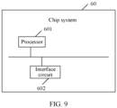
- an embodiment of this application further provides a chip system.
- the chip system 60 includes at least one processor 601 and at least one interface circuit 602.
- the at least one processor 601 and the at least one interface circuit 602 may be interconnected through a line.
- the processor 601 is configured to support the electronic device to implement various steps in the foregoing method embodiments, such as the methods shown in FIG. 4 and FIG. 5 .
- the at least one interface circuit 602 may be configured to receive signals from another apparatus (such as a memory), or to transmit signals to another apparatus (such as a communication interface).
- the chip system may include a chip, or may include other discrete devices.
- An embodiment of this application further provides a computer-readable storage medium, and the computer-readable storage medium includes instructions.
- the instructions when run on an electronic device, cause the electronic device to perform various steps in the foregoing method embodiments, such as the methods shown in FIG. 4 and FIG. 5 .
- An embodiment of this application further provides a computer program product including instructions.
- the instructions when run on an electronic device, cause the electronic device to perform various steps in the foregoing method embodiments, such as the methods shown in FIG. 4 and FIG. 5 .
- sequence numbers of the foregoing processes do not mean execution sequences in various embodiments of this application.
- the execution sequences of the processes should be determined according to functions and internal logic of the processes, and should not constitute any limitation on the implementation processes of the embodiments of this application.
- modules and algorithm steps may be implemented by electronic hardware or a combination of computer software and electronic hardware. Whether these functions are performed in the form of hardware or software depends on particular applications and design constraint conditions of the technical solutions. A person skilled in the art may use different methods to implement the described functions for each particular application, but it should not be considered that the implementation goes beyond the scope of this application.
- the disclosed system, device and method may be implemented in other manners.
- the described device embodiments are merely exemplary.
- division of the modules is merely logical function division and there may be other division manners during actual implementation.
- a plurality of modules or components may be combined or integrated into another device, or some features may be ignored or not performed.
- the displayed or discussed mutual couplings or direct couplings or communication connections may be implemented by using some interfaces.
- the indirect couplings or communication connections between the devices or modules may be implemented in electronic, mechanical, or other forms.
- modules described as separate components may or may not be physically separate, and components displayed as modules may or may not be physical modules, may be located in one device, or may be distributed on a plurality of devices. Some or all of the modules may be selected according to the actual needs to achieve the objectives of the solutions of the embodiments.
- All or some of the foregoing embodiments may be implemented by using software, hardware, firmware, or any combination thereof.
- a software program is used to implement the embodiments, the embodiments may be implemented in whole or in part in a form of a computer program product.
- the computer program product includes one or more computer instructions.
- the computer may be a general-purpose computer, a dedicated computer, a computer network, or any of other programmable apparatuses.
- the computer instructions may be stored in a computer-readable storage medium or transmitted from one computer-readable storage medium to another computer-readable storage medium.
- the computer instructions may be transmitted from one website, computer, server or data center to another website, computer, server or data center in a wired (for example, a coaxial cable, an optical fiber or a digital subscriber line (digital subscriber line, DSL)) or wireless (for example, infrared, wireless or microwave, etc.) manner.
- the computer-readable storage medium may be any usable medium accessible by a computer, or a data storage device, such as a server or a data center, integrating one or more usable media.
- the usable medium may be a magnetic medium (for example, a floppy disk, a hard disk, or a magnetic tape), an optical medium (for example, a DVD), a semiconductor medium (for example, a solid-state drive (Solid-State Drive, SSD)), or the like.
- a magnetic medium for example, a floppy disk, a hard disk, or a magnetic tape
- an optical medium for example, a DVD
- a semiconductor medium for example, a solid-state drive (Solid-State Drive, SSD)
Landscapes
- Engineering & Computer Science (AREA)
- Computer Networks & Wireless Communication (AREA)
- Signal Processing (AREA)
- Mobile Radio Communication Systems (AREA)
Abstract
Description
- This application claims priority to
Chinese Patent Application No. 202210993102.2, filed with the China National Intellectual Property Administration on August 18, 2022 - This application relates to the field of communication, and in particular to a wireless communication circuit, a Bluetooth communication switching method, and an electronic device.
- Among existing electronic devices such as mobile phones, Bluetooth (bluetooth, BT) and wireless fidelity (wireless fidelity, Wi-Fi) share an antenna in a time division manner. When the amount of data transmitted by Wi-Fi is large, it will reduce the communication rate of Bluetooth, thus influencing the communication quality of Bluetooth.
- Embodiments of this application disclose a wireless communication circuit, a Bluetooth communication switching method, and an electronic device, which are used for improving a communication quality of Bluetooth communication.
- To achieve the foregoing objective, the following technical solutions are used in the embodiments of this application:
According to a first aspect, a wireless communication circuit is provided. The wireless communication circuit includes: a processor, a switching circuit, a modulator demodulator (modulator demodulator, MDM), a first front-end module (front-end modules, FEM), and a second FEM. The processor is coupled to the switching circuit, the modulator demodulator and the first FEM, the modulator demodulator is coupled to the second FEM through the switching circuit, the first FEM supports wireless fidelity Wi-Fi communication or Bluetooth communication, and the second FEM supports cellular communication or Bluetooth communication; and the processor is configured to: acquire communication state information of the first FEM, where the communication state information is used for indicating whether the first FEM performs Wi-Fi communication; when the communication state information indicates that the first FEM performs Wi-Fi communication, transmit a first control command to the switching circuit, where the first control command is used for controlling the switching circuit to detect whether the modulator demodulator transmits a mobile industry processor interface (mobile industry processor interface, MIPI) command to the second FEM, and when the modulator demodulator does not transmit an MIPI command to the second FEM, control the second FEM to perform Bluetooth communication; and when the communication state information indicates that the first FEM does not perform Wi-Fi communication, transmit a second control command to the switching circuit, where the second control command is used for controlling the switching circuit to detect whether the modulator demodulator transmits an MIPI command to the second FEM, and when the modulator demodulator does not transmit an MIPI command to the second FEM, directly conduct the modulator demodulator with the second FEM so as to enable the modulator demodulator to control the second FEM to perform cellular communication. - In the wireless communication circuit provided in this embodiment of this application, the first FEM supports wireless fidelity Wi-Fi communication or Bluetooth communication; when the first FEM performs Wi-Fi communication and the MDM does not transmit an MIPI command to the second FEM, the second FEM is controlled to perform Bluetooth communication, thus switching some or all of Bluetooth communication of the first FEM to a relatively idle second FEM, preventing time-division multiplexing of Wi-Fi communication and Bluetooth communication from occupying resources for Bluetooth communication, and improving the communication quality of Bluetooth communication.
- In a possible implementation, the switching circuit includes a controller, an MIPI slave module, an MIPI master module, and a bypass gating circuit; the controller is coupled to the modulator demodulator through the MIPI slave module and the bypass gating circuit, and the controller is further coupled to the second FEM through the MIPI master module and the bypass gating circuit; the MIPI slave module is configured to convert an MIPI command from the modulator demodulator from a MIPI bus format to an on-chip bus format and transmit same to the controller; the MIPI master module is configured to convert an MIPI command from the controller from the on-chip bus format to the MIPI bus format and transmit same to the second FEM through the bypass gating circuit; the controller is configured to: when the first control command is received, control the bypass gating circuit to conduct the MIPI slave module with the modulator demodulator and conduct the MIPI master module with the second FEM, and detect whether the modulator demodulator transmits an MIPI command to the second FEM through the MIPI slave module, and when the modulator demodulator does not transmit an MIPI command to the second FEM, transmit a first MIPI command to the second FEM through the MIPI master module, where the first MIPI command is used for instructing the second FEM to perform Bluetooth communication; the controller is further configured to: when the second control command is received, detect whether the modulator demodulator transmits an MIPI command to the second FEM through the MIPI slave module, and when the modulator demodulator does not transmit an MIPI command to the second FEM, control the bypass gating circuit to directly conduct the modulator demodulator with the second FEM, and transmit a second MIPI command to the second FEM through the MIPI master module, where the second MIPI command is used for instructing the second FEM to perform cellular communication.
- This implementation discloses a possible implementation of how to implement a switching circuit.
- In a possible implementation, the controller is further configured to: after the first MIPI command is transmitted to the second FEM through the MIPI master module, receive and cache an MIPI command from the MDM through the MIPI slave module; and after the second MIPI command is transmitted to the second FEM through the MIPI master module, transmit the cached MIPI command from the modulator demodulator to the second FEM through the MIPI master module.
- This implementation ensures that the control logic between the modulator demodulator and the second FEM remains consistent before and after switching.
- In a possible implementation, the processor is specifically configured to: when the communication state information indicates that the first FEM performs Wi-Fi communication, transmit the first control command to the switching circuit after preset time.
- This implementation can prevent frequent switching of Bluetooth communication between the first FEM and the second FEM. The advantage of this solution is that determination conditions are simple and there will be no frequent switching from beginning to end.
- In a possible implementation, the processor is specifically configured to: when the communication state information indicates that the first FEM performs Wi-Fi communication and the number of times that the first FEM switches between performing Wi-Fi communication and skipping performing Wi-Fi communication within first preset time is less than a number threshold, transmit the first control command to the switching circuit.
- This implementation can prevent frequent switching of Bluetooth communication between the first FEM and the second FEM. The advantage of this solution is that it can detect more quickly, switch the state as soon as possible after connecting to Wi-Fi, and provide a better experience.
- In a possible implementation, the processor is further configured to: when the number of times that the first FEM switches between performing Wi-Fi communication and skipping performing Wi-Fi communication within the first preset time is greater than or equal to the number threshold, acquire the communication state information of the first FEM after second preset time.
- This implementation can avoid never switching the state, and can switch the state normally when the Wi-Fi connection is stable.
- According to a second aspect, a Bluetooth communication switching method is provided. The Bluetooth communication switching method includes: acquiring communication state information of a first FEM, where the first FEM supports wireless fidelity Wi-Fi communication or Bluetooth communication, and the communication state information is used for indicating whether the first FEM performs Wi-Fi communication; transmitting a first control command to a switching circuit when the communication state information indicates that the first FEM performs Wi-Fi communication, where the first control command is used for controlling the switching circuit to detect whether a modulator demodulator transmits a mobile industry processor interface MIPI command to a second FEM, and when the modulator demodulator does not transmit an MIPI command to the second FEM, controlling the second FEM to perform Bluetooth communication, where the second FEM supports cellular communication or Bluetooth communication; and when the communication state information indicates that the first FEM does not perform Wi-Fi communication, transmitting a second control command to the switching circuit, where the second control command is used for controlling the switching circuit to detect whether the modulator demodulator transmits an MIPI command to the second FEM, and when the modulator demodulator does not transmit an MIPI command to the second FEM, directly conducting the modulator demodulator with the second FEM so as to enable the modulator demodulator to control the second FEM to perform cellular communication.
- In a possible implementation, the method further includes: when the first control command is received, controlling a bypass gating circuit to conduct an MIPI slave module with the modulator demodulator and conduct an MIPI master module with the second FEM, and detecting whether the modulator demodulator transmits an MIPI command to the second FEM through the MIPI slave module, and when the modulator demodulator does not transmit an MIPI command to the second FEM, transmitting a first MIPI command to the second FEM through the MIPI master module, where the first MIPI command is used for instructing the second FEM to perform Bluetooth communication; and when the second control command is received, detecting whether the modulator demodulator transmits an MIPI command to the second FEM through the MIPI slave module, and when the modulator demodulator does not transmit an MIPI command to the second FEM, controlling the bypass gating circuit to directly conduct the modulator demodulator with the second FEM, and transmitting a second MIPI command to the second FEM through the MIPI master module, where the second MIPI command is used for instructing the second FEM to perform cellular communication.
- In a possible implementation, the method further includes: after the first MIPI command is transmitted to the second FEM through the MIPI master module, receiving and caching an MIPI command from the MDM through the MIPI slave module; and after the second MIPI command is transmitted to the second FEM through the MIPI master module, transmitting the cached MIPI command from the MDM to the second FEM through the MIPI master module.
- In a possible implementation, the transmitting a first control command to a switching circuit when the communication state information indicates that the first FEM performs Wi-Fi communication includes: when the communication state information indicates that the first FEM performs Wi-Fi communication, transmitting the first control command to the switching circuit after preset time.
- In a possible implementation, the transmitting a first control command to a switching circuit when the communication state information indicates that the first FEM performs Wi-Fi communication includes: when the communication state information indicates that the first FEM performs Wi-Fi communication and the number of times that the first FEM switches between performing Wi-Fi communication and skipping performing Wi-Fi communication within first preset time is less than a number threshold, transmitting the first control command to the switching circuit.
- In a possible implementation, the method further includes: when the number of times that the first FEM switches between performing Wi-Fi communication and skipping performing Wi-Fi communication within the first preset time is greater than or equal to the number threshold, acquiring the communication state information of the first FEM after second preset time.
- According to a third aspect, an electronic device is provided. The electronic device includes the wireless communication circuit according to the first aspect and any implementation thereof, or includes a processor and a memory. The memory stores instructions, and the method according to the second aspect or any implementation is performed when the processor executes the instructions.
- According to a fourth aspect, a computer-readable storage medium is provided. The computer-readable storage medium includes instructions. The instructions, when executed on an electronic device, cause an electronic device to perform the method according to the second aspect and any implementation thereof.
- According to a fifth aspect, a computer program product including instructions is provided. The instructions, when executed on an electronic device, cause the electronic device to perform the method according to the second aspect and any implementation thereof.
- According to a sixth aspect, a chip system is provided. The chip system includes a processor configured to support an electronic device to implement a function involved in the second aspect. In a possible design, the apparatus further includes an interface circuit. The interface circuit may be configured to receive signals from another apparatus (such as a memory) or transmit signals to another apparatus (such as a communication interface). The chip system may include a chip, or may include other discrete devices.
- For technical effects brought by the second aspect to the sixth aspect, refer to technical effects brought by the first aspect and any implementation thereof, which will not be repeated here.
-
-
FIG. 1 is a schematic structural diagram of an electronic device according to an embodiment of this application; -
FIG. 2 is a schematic structural diagram of another electronic device according to an embodiment of this application; -
FIG. 3 is a structural schematic diagram of a wireless communication circuit according to an embodiment of this application; -
FIG. 4 is a flowchart of a Bluetooth communication switching method according to an embodiment of this application; -
FIG. 5 is a flowchart of another Bluetooth communication switching method according to an embodiment of this application; -
FIG. 6 is a schematic diagram of a display interface according to an embodiment of this application; -
FIG. 7 is a schematic diagram of another display interface according to an embodiment of this application; -
FIG. 8 is a schematic diagram of yet another display interface according to an embodiment of this application; and -
FIG. 9 is a schematic structural diagram of a chip system according to an embodiment of this application. - First, some concepts involved in this application will be described below.
- In the embodiments of this application, terms such as "first" and "second" are merely used for distinguishing features of the same type, and cannot be understood as an indication of relative importance, a quantity, or a sequence.
- In the embodiments of this application, the terms "exemplary" or "for example" is used to represent giving an example, an illustration, or a description. Any embodiment or design scheme described as an "exemplary" or "for example" in this application should not be explained as being more preferred or having more advantages than another embodiment or design scheme. In particular, the terms such as "exemplary" and "for example" as used herein are intended to present the related concept in a specific implementation.
- In the embodiments of this application, the terms "couple" or "connection" should be understood in a broad sense. For example, the connection may be a physically direct connection, or an indirect connection realized through an electronic device, such as a connection realized through a resistor, an inductor, a capacitor, or other electronic devices.
- An embodiment of this application provides an electronic device. The electronic device may be a device with a display function. The electronic device may be mobile or fixed. The electronic device may be deployed on land (such as indoors or outdoors, either hand-held or vehicle-mounted, etc.), on water (such as ships, etc.), and in air (such as airplanes, balloons or satellites, etc.). The electronic device may be referred to as a user equipment (user equipment, UE), access terminal, terminal unit, subscriber unit (subscriber unit), terminal station, mobile station (mobile station, MS), movable station, terminal agent or terminal device, etc. For example, the terminal device may be a mobile phone, a tablet computer, a notebook computer, a smart bracelet, a smart watch, a headset, a smart speaker, a virtual reality (virtual reality, VR) device, an augmented reality (augmented reality, AR) device, a terminal related to industrial control (industrial control), a terminal related to self-driving (self-driving), a terminal related to remote medical (remote medical), a terminal related to a smart grid (smart grid), a terminal related to transportation safety (transportation safety), a terminal related to a smart city (smart city), a terminal related to a smart home (smart home), or the like. The specific type and structure of the electronic device are not limited in the embodiments of this application. A possible structure of the electronic device will be described below.
- Taking the electronic device being a mobile phone as an example,
FIG. 1 illustrates a possible structure of anelectronic device 101. Theelectronic device 101 may include aprocessor 210, anexternal memory interface 220, aninternal memory 221, a universal serial bus (universal serial bus, USB) interface 230, apower management module 240, abattery 241, awireless charging coil 242, anantenna 1, anantenna 2, amobile communication module 250, awireless communication module 260, anaudio module 270, aspeaker 270A, areceiver 270B, amicrophone 270C, aheadset jack 270D, asensor module 280, a key 290, amotor 291, anindicator 292, acamera 293, adisplay screen 294, a subscriber identification module (subscriber identification module, SIM)card interface 295, and the like. - The
sensor module 280 may include a pressure sensor, a gyro sensor, a barometric pressure sensor, a magnetic sensor, an acceleration sensor, a distance sensor, an optical proximity sensor, a fingerprint sensor, a temperature sensor, and a touch sensor, an ambient light sensor, a bone conduction sensor, and the like. - It may be understood that a schematic structure in this embodiment of this application does not constitute a specific limitation on the
electronic device 101. In some other embodiments of this application, theelectronic device 101 may include more or fewer components than those shown in the figure, or some components may be combined, or some components may be divided, or different component arrangements may be used. The components illustrated may be implemented by hardware, software, or a combination of software and hardware. - The
processor 210 may include one or more processing units. For example, theprocessor 210 may be a field programmable gate array (field programmable gate array, FPGA), an application specific integrated circuit (application specific integrated circuit, ASIC), a system on chip (system on chip, SoC), a central processing unit (central processing unit, CPU), an application processor (application processor, AP), a network processor (network processor, NP), a digital signal processor (digital signal processor, DSP), a micro controller unit (micro controller unit, MCU), a programmable logic device (programmable logic device, PLD), a modulation and demodulation processor, a graphics processing unit (graphics processing unit, GPU), an image signal processor (image signal processor, ISP), a controller, a video codec, a baseband processor, a neural-network processing unit (neural-network processing unit, NPU), or the like. Different processing units may be separate devices, or may be integrated into one or more processors. For example, theprocessor 210 may be an application processor AP. Alternatively, theprocessor 210 may be integrated into a system on chip (system on chip, SoC). Alternatively, theprocessor 210 may be integrated into an integrated circuit (integrated circuit, IC) chip. Theprocessor 210 may include an analog front end (analog front end, AFE) and a micro-controller unit (micro-controller unit, MCU) in an IC chip. - The controller may be a nerve center and a command center of the
electronic device 101. The controller may generate an operation control signal according to an instruction operation code and a time-sequence signal, and control obtaining and execution of instructions. - A memory may be further provided in the
processor 210 to store instructions and data. In some embodiments, the memory in theprocessor 210 is a cache memory. The memory may store instructions or data that is just used or cyclically used by theprocessor 210. If theprocessor 210 needs to use the instructions or data again, the processor may directly call the instructions or data from the memory. This avoids repeated access and reduces the waiting time of theprocessor 210, thus improving the system efficiency. - In some embodiments, the
processor 210 may include one or more interfaces. The interface may include an inter-integrated circuit (inter-integrated circuit, I2C) interface, an inter-integrated circuit sound (inter-integrated circuit sound, I2S) interface, a pulse code modulation (pulse code modulation, PCM) interface, a universal asynchronous receiver/transmitter (universal asynchronous receiver/transmitter, UART) interface, a mobile industry processor interface (mobile industry processor interface, MIPI), a general-purpose input/output (general-purpose input/output, GPIO) interface, a subscriber identity module (subscriber identity module, SIM) interface, and/or a USB interface. - It may be understood that an interface connection relationship between the modules illustrated in this embodiment of this application is merely an example for description, and does not constitute a limitation on a structure of the
electronic device 101. In some other embodiments of this application, theelectronic device 101 may alternatively use an interface connection manner different from that in the foregoing embodiment, or use a combination of a plurality of the interface connection manners. - The
power management module 240 is configured to receive a charging input from a charger. The charger may be a wireless charger (such as a wireless charging dock of theelectronic device 101 or other devices that can charge theelectronic device 101 wirelessly), or a wired charger. For example, thepower management module 240 may receive a charging input from the wired charger through the USB interface 230. Thepower management module 240 may receive a wireless charging input through thewireless charging coil 242 of the electronic device. - While charging the
battery 241, thepower management module 240 may further supply power to the electronic device. Thepower management module 240 receives an input from thebattery 241 to supply power to theprocessor 210, theinternal memory 221, theexternal memory interface 220, thedisplay screen 294, thecamera 293, thewireless communication module 260, and the like. Thepower management module 240 may be further configured to monitor parameters such as the battery capacity, cycle count, health state (leakage and impedance) of thebattery 241. In some other embodiments, thepower management module 240 may also be provided in theprocessor 210. - The wireless communication function of the
electronic device 101 may be implemented by using theantenna 1, theantenna 2, themobile communication module 250, thewireless communication module 260, the modulation and demodulation processor, the baseband processor, and the like. - The
electronic device 101 implements a display function by using the GPU, thedisplay screen 294, the application processor, and the like. The GPU is a microprocessor for image processing and connects thedisplay screen 294 and the application processor. The GPU is configured to perform mathematical and geometric calculation, and is configured to render graphics. Theprocessor 210 may include one or more GPUs, and execute program instructions to generate or change display information. - The
display screen 294 is configured to display an image, a video and the like. Thedisplay screen 294 includes a display panel and a touch screen. In some embodiments, theelectronic device 101 may include one or N display screens 294, where N is a positive integer greater than one. - The
electronic device 101 can implement a photographing function by using the ISP, thecamera 293, the video codec, the GPU, thedisplay screen 294, the application processor, and the like. The ISP is configured to process data fed back by thecamera 293. In some embodiments, the ISP may be provided in thecamera 293. Thecamera 293 is configured to capture a still image or video. In some embodiments, theelectronic device 101 may include one orN cameras 293, where N is a positive integer greater than one. - The
external memory interface 220 may be configured to connect to an external storage card, for example, a micro SanDisk (micro SanDisk, Micro SD) card, to expand the storage capability of theelectronic device 101. The external storage card communicates with theprocessor 210 by using theexternal memory interface 220, to implement a data storage function, for example, storing files such as music and videos into the external storage card. - The
internal memory 221 may be configured to store a computer-executable program code. The computer-executable program code includes instructions. Theprocessor 210 runs the instructions stored in theinternal memory 221, to implement various functional applications and data processing of theelectronic device 101. In addition, theinternal memory 221 may include a high-speed random access memory, and may also include a non-volatile memory, for example, at least one magnetic disk storage device, a flash memory device, a universal flash storage (universal flash storage, UFS), and the like. - The memory involved in the embodiments of this application may be a volatile memory or the non-volatile memory, or may include both the volatile memory and the non-volatile memory. The non-volatile memory may be a read-only memory (read-only memory, ROM), a programmable ROM (programmable ROM, PROM), an erasable PROM (erasable PROM, EPROM), an electrically EPROM (electrically EPROM, EEPROM) or a flash memory. The volatile memory may be a random access memory (random access memory, RAM), and is used as an external cache. Through exemplary but non-restrictive description, many forms of RAMs, such as static RAM (static RAM, SRAM), dynamic RAM (dynamic RAM, DRAM), synchronous DRAM (synchronous DRAM, SDRAM), double data rate SDRAM (double data rate SDRAM, DDR SDRAM), enhanced SDRAM (enhanced SDRAM, ESDRAM), synchlink DRAM (synchlink DRAM, SLDRAM), and direct rambus RAM (direct rambus RAM, DR RAM), may be used. It is to be understood that the memories involved in the systems and methods described herein are intended to include, but not limited to, these memories and memories of any other suitable type.
- The
electronic device 101 may implement an audio function by using theaudio module 270, thespeaker 270A, thereceiver 270B, themicrophone 270C, theheadset jack 270D, the application processor, and the like, for example, playing music or recording sounds. - The
audio module 270 is configured to convert digital audio information into analog audio signal outputs, and is also configured to convert analog audio inputs into digital audio signals. In some embodiments, theaudio module 270 may be provided in theprocessor 210, or some functional modules of theaudio module 270 may be provided in theprocessor 210. Thespeaker 270A, also referred to as "horn", is configured to convert an audio electrical signal into a sound signal. Thephone receiver 270B, also referred to as "receiver", is configured to convert an audio electrical signal into a sound signal. Themicrophone 270C, also referred to as "voice tube" or "mike", is configured to convert a sound signal into an electrical signal. At least onemicrophone 270C may be arranged in theelectronic device 101. Theheadset jack 270D is configured to be connected to a wired headset. Theheadset jack 270D may be a USB interface 230, or may be a 3.5 mm open mobile terminal platform (open mobile terminal platform, OMTP) standard interface, or a cellular telecommunications industry association of the USA (cellular telecommunications industry association of the USA, CTIA) standard interface. - The key 290 includes a power key, a volume key, and the like. The
button 290 may be a mechanical button. It may also be a touch button. Theelectronic device 101 may receive a button input, and generate a button signal input related to user setting and function control of theelectronic device 101. Themotor 291 may generate a vibration prompt. Themotor 291 may be used for an incoming call vibration prompt and touch vibration feedback. Theindicator 292 may be an indicator light, and may be configured to indicate a charging state or a battery change, or may be configured to indicate a message, a missed call, a notification, or the like. TheSIM card interface 295 is configured to connect an SIM card. The SIM card may be inserted into theSIM card interface 295 or plugged from theSIM card interface 295, to come into contact with or be separated from theelectronic device 101. Theelectronic device 101 may support one or N SIM card interfaces, where N is a positive integer greater than one. TheSIM card interface 295 can support a Nano SIM (Nano SIM) card, a Micro SIM (Micro SIM) card, an SIM card, and the like. In some embodiments, theelectronic device 101 uses an embedded SIM (embedded SIM, eSIM) card. The eSIM card may be embedded in theelectronic device 101 and cannot be separated from theelectronic device 101. - The
antenna 1 and theantenna 2 are configured to transmit and receive an electromagnetic wave signal. Each antenna in theelectronic device 101 may be configured to cover one or more communication frequency bands. Different antennas may further be multiplexed to improve the utilization rate of the antennas. For example, theantenna 1 may be multiplexed into a diversity antenna of a wireless local area network. In some other embodiments, the antennas may be used with a tuning switch. - The
mobile communication module 250 may provide a solution to wireless communication including 2G/3G/4G/5G applied to theelectronic device 101. Thewireless communication module 260 may provide a solution to wireless communication including wireless local area network (wireless local area networks, WLAN) (for example, wireless fidelity (wireless fidelity, Wi-Fi) network), Bluetooth (Bluetooth, BT), and global navigation satellite system (global navigation satellite system, GNSS), frequency modulation (frequency modulation, FM), near field communication (near field communication, NFC) technology, infrared (infrared, IR) technology, and the like applied to theelectronic device 101. In some embodiments, theantenna 1 and themobile communication module 250 of theelectronic device 101 are coupled, and theantenna 2 and thewireless communication module 260 are coupled, so that theelectronic device 101 can communicate with networks and another device through a wireless communication technology. - As shown in
FIG. 2 , in the existing technology, thewireless communication module 260 includes afirst FEM 261, and themobile communication module 250 includes anMDM 251 and asecond FEM 252. Thefirst FEM 261 and thesecond FEM 252 are configured to amplify a transmitted or received radio-frequency signal. TheMDM 251 is configured to modulate a baseband signal into a radio-frequency signal through digital signal modulation, and to demodulate a radio-frequency signal into a digital signal. Thesecond FEM 252 implements the transmission of radio frequency signals for mobile communication (i.e., cellular communication), while thefirst FEM 261 implements time-division transmission of radio frequency signals for Wi-Fi and Bluetooth. When a user enters indoors from outside and allows the electronic device to perform Wi-Fi communication, the amount of data transmitted by the electronic device through Wi Fi is relatively large, while the amount transmitted through cellular communication is relatively small. Due to the shared FEM and antenna between Wi-Fi and Bluetooth, the communication rate of Bluetooth will be reduced, thus causing an influence to the communication quality of Bluetooth, such as a decrease in call quality of Bluetooth headset, a decrease in Bluetooth data transmission rate, etc. - In regard to this, an embodiment of this application provides a wireless communication circuit applied to the electronic devices, which can reduce or prevent the influence on the communication rate of Bluetooth by occupying the FEM and antenna of cellular communication through Bluetooth.
- As shown in
FIG. 3 , the wireless communication circuit includes aprocessor 31, a switchingcircuit 32, anMDM 33, afirst FEM 34, and asecond FEM 35. The switchingcircuit 32 includes a serial peripheral interface (serial peripheral interface, SPI)module 321, acontroller 322, a mobile industry processor interface (mobile industry processor interface, MIPI)slave module 323, anMIPI master module 324, and a bypass (bypass) gatingcircuit 325. Theprocessor 31 is coupled to the switchingcircuit 32, theMDM 33 and thefirst FEM 34. Theprocessor 31 is coupled to thecontroller 322 through theSPI module 321 in the switchingcircuit 32. TheMDM 33 is coupled to thesecond FEM 35 through the switchingcircuit 32. TheMDM 33, the switchingcircuit 32 and thesecond FEM 35 perform communication with each other by using an MIPI bus. - The
first FEM 34 and thesecond FEM 35 are configured to amplify a transmitted or received radio-frequency signal. Thefirst FEM 34 can support time-division multiplexing of Wi-Fi communication or Bluetooth communication, while thesecond FEM 35 can support cellular communication or Bluetooth communication. - The
MDM 33 is configured to transmit an MIPI command to thesecond FEM 35 to control thesecond FEM 35 to perform cellular communication. TheMDM 33 is further configured to generate a radio-frequency signal from a baseband signal through digital signal modulation, transmit same to the outside through thesecond FEM 35, and demodulate a radio-frequency signal received through thesecond FEM 35 to obtain a digital signal. TheMDM 33 is further configured to transmit the communication state information of thesecond FEM 35 to theprocessor 31. - The
SPI module 321 is configured to implement serial communication between theprocessor 31 and thecontroller 322. - The
bypass gating circuit 325 is controlled by thecontroller 322, and is configured to directly conduct theMDM 33 with the second FEM 35 (a path indicated by the dashed arrow in the figure), or conduct theMDM 33 with thecontroller 322 through theMIPI slave module 323, and conduct thecontroller 322 with thesecond FEM 35 through the MIPI master module 324 (a path indicated by the solid arrow in the figure). Thebypass gating circuit 325 can be implemented through an analog circuit such as complementary metal oxide semiconductor (complementary metal oxide semiconductor, CMOS) or through a Verilog register transfer level (register transfer level, RTL) code, which is not limited here. - The
MIPI slave module 323 is connected with theMDM 33 by using an MIPI bus. TheMIPI slave module 323 is connected with thecontroller 322 by using an on-chip bus (such as an advanced high performance bus (advanced high performance bus, AHB) bus). TheMIPI slave module 323 is configured to convert an MIPI command (such as a first MIPI command involved later) from theMDM 33 from the MIPI bus format to the on-chip bus format and transmit same to thecontroller 322. - The
MIPI master module 324 is connected with thesecond FEM 35 through the MIPI bus. TheMIPI master module 324 is connected with thecontroller 322 through the on-chip bus. TheMIPI master module 324 is configured to convert an MIPI command (such as a second MIPI command involved later) from thecontroller 322 from the on-chip bus format to the MIPI bus format and transmit same to thesecond FEM 35. - The
processor 31 can acquire communication state information of thefirst FEM 34, such as whether it performs Wi-Fi communication (or performs Wi-Fi communication or Bluetooth communication). Theprocessor 31 can also acquire communication state information of thesecond FEM 35, such as whether it performs cellular communication. Theprocessor 31 can also transmit a first control command or a second control command (as specifically described later) to thecontroller 322 in the switchingcircuit 32 through theSPI module 321 according to the communication state information of thefirst FEM 34, to control thesecond FEM 35 to switch between a cellular communication state and a Bluetooth communication state through the switchingcircuit 32. - The
controller 322 is configured to control thebypass gating circuit 325 to switch between a bypass mode and a non-bypass mode according to the first control command or second control command from theprocessor 31. - Specifically, the wireless communication circuit can perform a Bluetooth communication switching method described in this application, and as shown in
FIG. 4 , the method includes the following steps: - In S101, a
processor 31 acquires communication state information of afirst FEM 34. - The communication state information of the
first FEM 34 is used for indicating whether thefirst FEM 34 performs Wi-Fi communication, or the communication state information of thefirst FEM 34 is used for indicating whether thefirst FEM 34 performs Wi-Fi communication or performing Bluetooth communication. - In S102, when the communication state information of the
first FEM 34 indicates that thefirst FEM 34 performs Wi-Fi communication (or referred to as establishing a Wi-Fi connection), theprocessor 31 transmits a first control command to acontroller 322 in aswitching circuit 32. - The first control command is used for controlling the switching
circuit 32 to detect whether anMDM 33 transmits an MIPI command to asecond FEM 35. When theMDM 33 does not transmit an MIPI command to thesecond FEM 35, the switchingcircuit 32 controls thesecond FEM 35 to perform Bluetooth communication. - As shown in S1021-S1025 in
FIG. 5 , in a bypass mode, when thecontroller 322 in the switchingcircuit 32 receives the first control command from theprocessor 31, thecontroller 322 configures a mode switching register to a non-bypass mode and controls abypass gating circuit 325 to switch to the non-bypass mode. Thecontroller 322 controls thebypass gating circuit 325 to conduct anMIPI slave module 323 with theMDM 251, and to conduct anMIPI master module 324 with thesecond FEM 35. Thecontroller 322 detects whether theMDM 251 transmits an MIPI command to thesecond FEM 35 through theMIPI slave module 323. When it is detected that theMDM 251 does not transmit an MIPI command to the second FEM 35 (that is, the MIPI bus is idle), thecontroller 322 transmits a first MIPI command to thesecond FEM 35 through theMIPI master module 324. When it is detected that theMDM 251 transmits an MIPI command to thesecond FEM 35, it continues to wait until the MIPI bus is idle. The detected MIPI command from theMDM 251 may be any MIPI command. The first MIPI command is used for instructing thesecond FEM 35 to perform Bluetooth communication. That is to say, during the period that theMDM 251 does not transmit an MIPI command to thesecond FEM 35, thecontroller 322 switches thesecond FEM 35 from a cellular communication state to a Bluetooth communication state to avoid competing with theMDM 251 for the MIPI bus, thus avoiding transmission errors. - After the
controller 322 transmits the first MIPI command to thesecond FEM 35 through theMIPI master module 324 to instruct thesecond FEM 35 to perform Bluetooth communication, thecontroller 322 continues to receive and cache an MIPI command from theMDM 251 through theMIPI slave module 323. When thecontroller 322 controls thesecond FEM 35 to switch back to the Bluetooth communication state, the cached MIPI command from theMDM 251 is transmitted to thesecond FEM 35 through theMIPI master module 324, so that the control logic between theMDM 251 and thesecond FEM 35 remains consistent before and after switching. - In addition, due to unstable Wi-Fi connections in certain scenarios, in order to prevent frequent switching of Bluetooth communication between the
first FEM 34 and thesecond FEM 35, theprocessor 31 may determine whether to switch Bluetooth communication according to the time that thefirst FEM 34 performs Wi Fi communication. Alternatively, theprocessor 31 may determine whether to switch Bluetooth communication according to the number of times that thefirst FEM 34 switches between performing Wi-Fi communication and skipping performing Wi-Fi communication within preset time. - In a possible implementation, when the communication state information of the
first FEM 34 indicates that thefirst FEM 34 performs Wi-Fi communication, theprocessor 31 transmits a first control command to thecontroller 322 in the switchingcircuit 32 after preset time (for example, one minute). That is, after the electronic device is stably connected to the Wi-Fi connection for preset time, theprocessor 31 transmits a first control command to thecontroller 322 in the switchingcircuit 32. The advantages of this solution are that determination conditions are simple and frequent switching will not occur from beginning to end. - In another possible implementation, when the communication state information of the
first FEM 34 indicates that thefirst FEM 34 performs Wi-Fi communication and the number of times that thefirst FEM 34 switches between performing Wi-Fi communication and skipping performing Wi-Fi communication within first preset time (for example, 10 seconds) is less than a number threshold (for example, three times), theprocessor 31 transmits the first control command to thecontroller 322 in the switchingcircuit 32. When the number of times that thefirst FEM 34 switches between performing Wi-Fi communication and skipping performing Wi-Fi communication within the first preset time is greater than or equal to the number threshold, theprocessor 31 acquires the communication state information of thefirst FEM 34 after second preset time (for example, five minutes), so as to determine again whether to transmit the first control command. The advantage of this solution is that it can detect more quickly, switch the state as soon as possible after connecting to Wi-Fi, and provide a better experience. - Since the electronic device can support Bluetooth communication (or pairing) with multiple other devices, the
processor 31 can switch all or some of Bluetooth communication from thefirst FEM 34 to thesecond FEM 35 to improve the quality of Bluetooth communication. Exemplarily, as shown inFIG. 6 , the improvement of the quality of Bluetooth communication may be indicated by the change of the Bluetooth icon in the state bar of the electronic device from A to B, and the improvement of the quality of Bluetooth communication may also be indicated by the change of the Bluetooth icon from C to D in the drop-down menu, where A and C represent ordinary Bluetooth communication functions, and B and D represent enhanced Bluetooth communication functions. As shown inFIG. 7 , a Bluetooth pairing interface can be enabled by clicking on the triangle icon next to the Bluetooth icon in the drop-down menu, which displays different Bluetooth devices connected through different antennas. As shown inFIG. 8 , whether a Bluetooth enhancement function switch is turned on may be displayed in a Bluetooth settings menu. When the Bluetooth enhancement function switch is turned on, the electronic device can perform the Bluetooth communication switching method according to this application, and can display different Bluetooth devices connected through different antennas. When the Bluetooth enhancement function switch is turned off, the electronic device does not perform the Bluetooth communication switching method according to this application. - In S103, when the communication state information of the
first FEM 34 indicates that thefirst FEM 34 does not perform Wi-Fi communication (or referred to as disconnecting a Wi-Fi connection), theprocessor 31 transmits a second control command to thecontroller 322 in the switchingcircuit 32. - The second control command is used for controlling the switching
circuit 32 to detect whether theMDM 33 transmits an MIPI command to thesecond FEM 35. When theMDM 33 does not transmit an MIPI command to thesecond FEM 35, the switchingcircuit 32 directly conducts theMDM 33 with thesecond FEM 35, so that theMDM 33 controls thesecond FEM 35 to perform cellular communication. - As shown in S1031-S1034 in
FIG. 5 , in the non-bypass mode, when thecontroller 322 in the switchingcircuit 32 receives the second control command from theprocessor 31, thecontroller 322 configures the mode switching register to the bypass mode and controls thebypass gating circuit 325 to switch to the bypass mode. At this time, thecontroller 322 detects whether theMDM 251 transmits an MIPI command to thesecond FEM 35 through theMIPI slave module 323. When it is detected that theMDM 251 does not transmit an MIPI command to the second FEM 35 (that is, the MIPI bus is idle), thecontroller 322 controls thebypass gating circuit 325 to directly conduct theMDM 251 with thesecond FEM 35, and transmits a second MIPI command to thesecond FEM 35 through theMIPI master module 324. The second MIPI command is used for instructing thesecond FEM 35 to perform cellular communication. Therefore, theMDM 251 can control thesecond FEM 35 to perform cellular communication. When it is detected that theMDM 251 transmits an MIPI command to thesecond FEM 35, it continues to wait until the MIPI bus is idle. That is to say, during the period that theMDM 251 does not transmit an MIPI command to thesecond FEM 35, thecontroller 322 switches thesecond FEM 35 from a Bluetooth communication state to a cellular communication state to avoid competing with theMDM 251 for the MIPI bus, thus avoiding transmission errors. - After the
controller 322 transmits the second MIPI command to thesecond FEM 35 through theMIPI master module 324 to instruct thesecond FEM 35 to perform cellular communication, it also needs to transmit the previously cached MIPI command from theMDM 251 to thesecond FEM 35 through theMIPI master module 324, so that the control logic between theMDM 251 and thesecond FEM 35 remains consistent before and after switching. - In the wireless communication circuit, the Bluetooth communication switching method and the electronic device provided in the embodiments of this application, the first FEM supports wireless fidelity Wi-Fi communication or Bluetooth communication; when the first FEM performs Wi-Fi communication and the MDM does not transmit an MIPI command to the second FEM, the second FEM is controlled to perform Bluetooth communication, thus switching some or all of Bluetooth communication of the first FEM to a relatively idle second FEM, preventing time-division multiplexing of Wi-Fi communication and Bluetooth communication from occupying resources for Bluetooth communication, and improving the communication quality of Bluetooth communication.
- As shown in
FIG. 9 , an embodiment of this application further provides a chip system. Thechip system 60 includes at least oneprocessor 601 and at least oneinterface circuit 602. The at least oneprocessor 601 and the at least oneinterface circuit 602 may be interconnected through a line. Theprocessor 601 is configured to support the electronic device to implement various steps in the foregoing method embodiments, such as the methods shown inFIG. 4 andFIG. 5 . The at least oneinterface circuit 602 may be configured to receive signals from another apparatus (such as a memory), or to transmit signals to another apparatus (such as a communication interface). The chip system may include a chip, or may include other discrete devices. - An embodiment of this application further provides a computer-readable storage medium, and the computer-readable storage medium includes instructions. The instructions, when run on an electronic device, cause the electronic device to perform various steps in the foregoing method embodiments, such as the methods shown in
FIG. 4 andFIG. 5 . - An embodiment of this application further provides a computer program product including instructions. The instructions, when run on an electronic device, cause the electronic device to perform various steps in the foregoing method embodiments, such as the methods shown in
FIG. 4 andFIG. 5 . - For the technical effects of the chip system, the computer-readable storage medium and the computer program product, a reference may be made to the technical effects of the above-mentioned method embodiments.
- It should be understood that sequence numbers of the foregoing processes do not mean execution sequences in various embodiments of this application. The execution sequences of the processes should be determined according to functions and internal logic of the processes, and should not constitute any limitation on the implementation processes of the embodiments of this application.
- A person of ordinary skill in the art may be aware that, in combination with the examples described in the embodiments disclosed in this specification, modules and algorithm steps may be implemented by electronic hardware or a combination of computer software and electronic hardware. Whether these functions are performed in the form of hardware or software depends on particular applications and design constraint conditions of the technical solutions. A person skilled in the art may use different methods to implement the described functions for each particular application, but it should not be considered that the implementation goes beyond the scope of this application.
- A person skilled in the art may clearly understand that, for the objective of convenient and brief description, for a detailed working process of the system, apparatus, and module described above, refer to a corresponding process in the method embodiments, and details are not described herein again.
- In the several embodiments provided in this application, it should be understood that the disclosed system, device and method may be implemented in other manners. For example, the described device embodiments are merely exemplary. For example, division of the modules is merely logical function division and there may be other division manners during actual implementation. For example, a plurality of modules or components may be combined or integrated into another device, or some features may be ignored or not performed. In addition, the displayed or discussed mutual couplings or direct couplings or communication connections may be implemented by using some interfaces. The indirect couplings or communication connections between the devices or modules may be implemented in electronic, mechanical, or other forms.
- The modules described as separate components may or may not be physically separate, and components displayed as modules may or may not be physical modules, may be located in one device, or may be distributed on a plurality of devices. Some or all of the modules may be selected according to the actual needs to achieve the objectives of the solutions of the embodiments.
- In addition, functional modules in the embodiments of this application may be integrated into one device, or each of the modules may exist alone physically, or two or more modules may be integrated into one device.
- All or some of the foregoing embodiments may be implemented by using software, hardware, firmware, or any combination thereof. When a software program is used to implement the embodiments, the embodiments may be implemented in whole or in part in a form of a computer program product. The computer program product includes one or more computer instructions. When the computer program instructions are loaded and executed on a computer, all or some of the processes or functions according to the embodiments of this application are produced. The computer may be a general-purpose computer, a dedicated computer, a computer network, or any of other programmable apparatuses. The computer instructions may be stored in a computer-readable storage medium or transmitted from one computer-readable storage medium to another computer-readable storage medium. For example, the computer instructions may be transmitted from one website, computer, server or data center to another website, computer, server or data center in a wired (for example, a coaxial cable, an optical fiber or a digital subscriber line (digital subscriber line, DSL)) or wireless (for example, infrared, wireless or microwave, etc.) manner. The computer-readable storage medium may be any usable medium accessible by a computer, or a data storage device, such as a server or a data center, integrating one or more usable media. The usable medium may be a magnetic medium (for example, a floppy disk, a hard disk, or a magnetic tape), an optical medium (for example, a DVD), a semiconductor medium (for example, a solid-state drive (Solid-State Drive, SSD)), or the like.
- The foregoing descriptions are merely specific implementations of this application, but are not intended to limit the scope of protection of this application. Any variation or replacement readily figured out by a person skilled in the art within the technical scope disclosed in this application shall fall within the scope of protection of this application. Therefore, the scope of protection of this application shall be subject to the scope of protection of the claims.
Claims (14)
- A wireless communication circuit, comprising: a processor, a switching circuit, a modulator demodulator, a first front-end module FEM, and a second FEM, wherein the processor is coupled to the switching circuit, the modulator demodulator and the first FEM, the modulator demodulator is coupled to the second FEM through the switching circuit, the first FEM supports wireless fidelity Wi-Fi communication or Bluetooth communication, and the second FEM supports cellular communication or Bluetooth communication; and the processor is configured to:acquire communication state information of the first FEM, wherein the communication state information is used for indicating whether the first FEM performs Wi-Fi communication;when the communication state information indicates that the first FEM performs Wi-Fi communication, transmit a first control command to the switching circuit, wherein the first control command is used for controlling the switching circuit to detect whether the modulator demodulator transmits a mobile industry processor interface MIPI command to the second FEM, and when the modulator demodulator does not transmit an MIPI command to the second FEM, control the second FEM to perform Bluetooth communication; andwhen the communication state information indicates that the first FEM does not perform Wi-Fi communication, transmit a second control command to the switching circuit, wherein the second control command is used for controlling the switching circuit to detect whether the modulator demodulator transmits an MIPI command to the second FEM, and when the modulator demodulator does not transmit an MIPI command to the second FEM, directly conduct the modulator demodulator with the second FEM so as to enable the modulator demodulator to control the second FEM to perform cellular communication.
- The wireless communication circuit according to claim 1, wherein the switching circuit comprises a controller, an MIPI slave module, an MIPI master module, and a bypass gating circuit; the controller is coupled to the modulator demodulator through the MIPI slave module and the bypass gating circuit, and the controller is further coupled to the second FEM through the MIPI master module and the bypass gating circuit;the MIPI slave module is configured to convert an MIPI command from the modulator demodulator from a MIPI bus format to an on-chip bus format and transmit same to the controller; the MIPI master module is configured to convert an MIPI command from the controller from the on-chip bus format to the MIPI bus format and transmit same to the second FEM through the bypass gating circuit;the controller is configured to: when the first control command is received, control the bypass gating circuit to conduct the MIPI slave module with the modulator demodulator and conduct the MIPI master module with the second FEM, and detect whether the modulator demodulator transmits an MIPI command to the second FEM through the MIPI slave module, and when the modulator demodulator does not transmit an MIPI command to the second FEM, transmit a first MIPI command to the second FEM through the MIPI master module, wherein the first MIPI command is used for instructing the second FEM to perform Bluetooth communication; andthe controller is further configured to: when the second control command is received, detect whether the modulator demodulator transmits an MIPI command to the second FEM through the MIPI slave module, and when the modulator demodulator does not transmit an MIPI command to the second FEM, control the bypass gating circuit to directly conduct the modulator demodulator with the second FEM, and transmit a second MIPI command to the second FEM through the MIPI master module, wherein the second MIPI command is used for instructing the second FEM to perform cellular communication.
- The wireless communication circuit according to claim 2, wherein the controller is further configured to:after the first MIPI command is transmitted to the second FEM through the MIPI master module, receive and cache an MIPI command from the modulator demodulator through the MIPI slave module; andafter the second MIPI command is transmitted to the second FEM through the MIPI master module, transmit the cached MIPI command from the modulator demodulator to the second FEM through the MIPI master module.
- The wireless communication circuit according to any one of claims 1 to 3, wherein the processor is specifically configured to:
when the communication state information indicates that the first FEM performs Wi-Fi communication, transmit the first control command to the switching circuit after preset time. - The wireless communication circuit according to any one of claims 1 to 4, wherein the processor is specifically configured to:
when the communication state information indicates that the first FEM performs Wi-Fi communication and the number of times that the first FEM switches between performing Wi-Fi communication and skipping performing Wi-Fi communication within first preset time is less than a number threshold, transmit the first control command to the switching circuit. - The wireless communication circuit according to claim 5, wherein the processor is further configured to:
when the number of times that the first FEM switches between performing Wi-Fi communication and skipping performing Wi-Fi communication within the first preset time is greater than or equal to the number threshold, acquire the communication state information after second preset time. - A Bluetooth communication switching method, comprising:acquiring communication state information of a first front-end module FEM, wherein the first FEM supports wireless fidelity Wi-Fi communication or Bluetooth communication, and the communication state information is used for indicating whether the first FEM performs Wi-Fi communication;transmitting a first control command to a switching circuit when the communication state information indicates that the first FEM performs Wi-Fi communication, wherein the first control command is used for controlling the switching circuit to detect whether a modulator demodulator transmits a mobile industry processor interface MIPI command to a second FEM, and when the modulator demodulator does not transmit an MIPI command to the second FEM, controlling the second FEM to perform Bluetooth communication, wherein the second FEM supports cellular communication or Bluetooth communication; andwhen the communication state information indicates that the first FEM does not perform Wi-Fi communication, transmitting a second control command to the switching circuit, wherein the second control command is used for controlling the switching circuit to detect whether the modulator demodulator transmits an MIPI command to the second FEM, and when the modulator demodulator does not transmit an MIPI command to the second FEM, directly conducting the modulator demodulator with the second FEM so as to enable the modulator demodulator to control the second FEM to perform cellular communication.
- The method according to claim 7, wherein the method further comprises:when the first control command is received, controlling a bypass gating circuit to conduct an MIPI slave module with the modulator demodulator and conduct an MIPI master module with the second FEM, and detecting whether the modulator demodulator transmits an MIPI command to the second FEM through the MIPI slave module, and when the modulator demodulator does not transmit an MIPI command to the second FEM, transmitting a first MIPI command to the second FEM through the MIPI master module, wherein the first MIPI command is used for instructing the second FEM to perform Bluetooth communication; andwhen the second control command is received, detecting whether the modulator demodulator transmits an MIPI command to the second FEM through the MIPI slave module, and when the modulator demodulator does not transmit an MIPI command to the second FEM, controlling the bypass gating circuit to directly conduct the modulator demodulator with the second FEM, and transmitting a second MIPI command to the second FEM through the MIPI master module, wherein the second MIPI command is used for instructing the second FEM to perform cellular communication.
- The method according to claim 8, wherein the method further comprises:after the first MIPI command is transmitted to the second FEM through the MIPI master module, receiving and caching an MIPI command from the modulator demodulator through the MIPI slave module; andafter the second MIPI command is transmitted to the second FEM through the MIPI master module, transmitting the cached MIPI command from the modulator demodulator to the second FEM through the MIPI master module.
- The method according to any one of claims 7 to 9, wherein the transmitting a first control command to a switching circuit when the communication state information indicates that the first FEM performs Wi-Fi communication comprises:
when the communication state information indicates that the first FEM performs Wi-Fi communication, transmitting the first control command to the switching circuit after preset time. - The method according to any one of claims 7 to 10, wherein the transmitting a first control command to a switching circuit when the communication state information indicates that the first FEM performs Wi-Fi communication comprises:
when the communication state information indicates that the first FEM performs Wi-Fi communication and the number of times that the first FEM switches between performing Wi-Fi communication and skipping performing Wi-Fi communication within first preset time is less than a number threshold, transmitting the first control command to the switching circuit. - The method according to claim 11, wherein the method further comprises:
when the number of times that the first FEM switches between performing Wi-Fi communication and skipping performing Wi-Fi communication within the first preset time is greater than or equal to the number threshold, acquiring the communication state information after second preset time. - An electronic device, comprising the wireless communication circuit according to any one of claims 1 to 6, or comprising a processor and a memory, wherein the memory stores instructions, and the method according to any one of claims 7 to 12 is performed when the processor executes the instructions.
- A computer-readable storage medium, comprising instructions, wherein the instructions, when executed on an electronic device, cause the electronic device to perform the method according to any one of claims 7 to 12.
Applications Claiming Priority (2)
| Application Number | Priority Date | Filing Date | Title |
|---|---|---|---|
| CN202210993102.2A CN116054870B (en) | 2022-08-18 | 2022-08-18 | Wireless communication circuit, bluetooth communication switching method and electronic equipment |
| PCT/CN2023/090369 WO2024037025A1 (en) | 2022-08-18 | 2023-04-24 | Wireless communication circuit, bluetooth communication switching method, and electronic device |
Publications (3)
| Publication Number | Publication Date |
|---|---|
| EP4460149A1 true EP4460149A1 (en) | 2024-11-06 |
| EP4460149A4 EP4460149A4 (en) | 2025-06-25 |
| EP4460149B1 EP4460149B1 (en) | 2026-04-22 |
Family
ID=86126001
Family Applications (1)
| Application Number | Title | Priority Date | Filing Date |
|---|---|---|---|
| EP23853933.2A Active EP4460149B1 (en) | 2022-08-18 | 2023-04-24 | Wireless communication circuit, bluetooth communication switching method, and electronic device |
Country Status (4)
| Country | Link |
|---|---|
| US (1) | US20250175208A1 (en) |
| EP (1) | EP4460149B1 (en) |
| CN (3) | CN116054870B (en) |
| WO (1) | WO2024037025A1 (en) |
Families Citing this family (2)
| Publication number | Priority date | Publication date | Assignee | Title |
|---|---|---|---|---|
| CN116054870B (en) * | 2022-08-18 | 2023-10-20 | 荣耀终端有限公司 | Wireless communication circuit, bluetooth communication switching method and electronic equipment |
| CN118764044B (en) * | 2024-09-06 | 2025-03-14 | 荣耀终端股份有限公司 | Radio frequency circuit, power control method and electronic equipment |
Family Cites Families (22)
| Publication number | Priority date | Publication date | Assignee | Title |
|---|---|---|---|---|
| CN102026322A (en) * | 2009-09-23 | 2011-04-20 | 中兴通讯股份有限公司 | Method and system for voice switching |
| CN102548045A (en) * | 2010-12-22 | 2012-07-04 | 北京格林思通科技有限公司 | Short-distance wireless relaying method and system |
| US20120329395A1 (en) * | 2011-06-27 | 2012-12-27 | Qualcomm Atheros, Inc. | Dynamic antenna sharing |
| US20130267224A1 (en) * | 2012-04-10 | 2013-10-10 | Jyotsna KRISHNASWAMY | Apparatus and method for efficient location-based seamless modem and mobile application activation |
| US20140226502A1 (en) * | 2013-02-13 | 2014-08-14 | Qualcomm Incorporated | Coexistence of cellular and connectivity networks with global navigation satellite systems |
| US9497799B2 (en) * | 2013-10-04 | 2016-11-15 | Mediatek Inc. | Method for controlling RF signal processing components and communications apparatus utilizing the same |
| KR102224156B1 (en) * | 2014-04-02 | 2021-03-08 | 엘지전자 주식회사 | Mobile terminal and method for controlling the same |
| US10135482B2 (en) * | 2016-03-23 | 2018-11-20 | Avago Technologies General Ip (Singapore) Pte. Ltd. | Wireless transceiver with remote frontend |
| CA3040975C (en) * | 2016-10-21 | 2023-09-05 | Novaresp Technologies Inc. | Method and apparatus for breathing assistance |
| KR102374338B1 (en) * | 2017-09-07 | 2022-03-17 | 삼성전자주식회사 | An electronic device for transmitting and receiving data in a wireless communication system and a method thereof |
| US10757561B2 (en) * | 2019-03-29 | 2020-08-25 | Intel Corporation | Wi-Fi docking in dense environment |
| CN112020130B (en) * | 2019-05-30 | 2021-12-28 | 华为技术有限公司 | Interference processing method and equipment |
| US11516757B2 (en) * | 2019-06-07 | 2022-11-29 | Intel Corporation | Multi-access point collaboration in wireless communications |
| CN112399390B (en) * | 2019-08-14 | 2021-10-15 | 华为技术有限公司 | Method and related device for Bluetooth back-up connection |
| US10701538B1 (en) * | 2019-08-19 | 2020-06-30 | Bose Corporation | Smart connection management |
| CN111314921A (en) * | 2020-02-28 | 2020-06-19 | 恒安嘉新(北京)科技股份公司 | Test system, method, device and storage medium based on wireless communication |
| CN111556476B (en) * | 2020-04-17 | 2021-01-19 | 炬力(珠海)微电子有限公司 | Data transmission method between Bluetooth TWS (two way communication) devices and Bluetooth TWS devices |
| CN113676269B (en) * | 2020-05-15 | 2022-11-04 | 华为技术有限公司 | Data transmission method of electronic equipment, its medium and electronic equipment |
| CN112468179B (en) * | 2020-11-30 | 2022-05-24 | 维沃移动通信有限公司 | Radio frequency circuit, electronic device and control method thereof |
| CN113038440B (en) * | 2021-03-15 | 2023-04-07 | 杭州涂鸦信息技术有限公司 | Communication channel switching method and device, computer equipment and readable storage medium |
| US11265052B1 (en) * | 2021-04-13 | 2022-03-01 | Dell Products, Lp | System and method for antenna reduction and usage for a multi-radio information handling system |
| CN116054870B (en) * | 2022-08-18 | 2023-10-20 | 荣耀终端有限公司 | Wireless communication circuit, bluetooth communication switching method and electronic equipment |
-
2022
- 2022-08-18 CN CN202210993102.2A patent/CN116054870B/en active Active
- 2022-08-18 CN CN202311234475.2A patent/CN117335830B/en active Active
-
2023
- 2023-04-24 WO PCT/CN2023/090369 patent/WO2024037025A1/en not_active Ceased
- 2023-04-24 CN CN202380060628.8A patent/CN119769174A/en active Pending
- 2023-04-24 US US18/840,683 patent/US20250175208A1/en active Pending
- 2023-04-24 EP EP23853933.2A patent/EP4460149B1/en active Active
Also Published As
| Publication number | Publication date |
|---|---|
| CN117335830A (en) | 2024-01-02 |
| WO2024037025A1 (en) | 2024-02-22 |
| CN119769174A (en) | 2025-04-04 |
| CN116054870B (en) | 2023-10-20 |
| CN116054870A (en) | 2023-05-02 |
| CN117335830B (en) | 2024-08-16 |
| EP4460149B1 (en) | 2026-04-22 |
| US20250175208A1 (en) | 2025-05-29 |
| EP4460149A4 (en) | 2025-06-25 |
Similar Documents
| Publication | Publication Date | Title |
|---|---|---|
| CN108093134B (en) | Anti-interference method for electronic equipment and related products | |
| WO2021008614A1 (en) | Method for establishing communication connection and wearable device | |
| US11903054B2 (en) | Method for establishing communication connection and related products | |
| EP4460149B1 (en) | Wireless communication circuit, bluetooth communication switching method, and electronic device | |
| CN113489844B (en) | Volume gear adjusting method and electronic equipment | |
| WO2021129128A1 (en) | Wireless charging method for mobile terminal and mobile terminal | |
| CN113691678B (en) | Call control method, electronic device, computer readable storage medium and chip system | |
| US20230336654A1 (en) | Display method and electronic device | |
| CN115733921B (en) | TWS headset decoupling sharing method, device, equipment, storage medium and program product | |
| JP2024529908A (en) | Signal receiving method, device, user equipment, base station and storage medium | |
| CN118695343B (en) | Measurement relaxation method, device, storage medium and apparatus | |
| CN116056016B (en) | Prototype information reporting method and electronic equipment | |
| CN113407076A (en) | Method for starting application and electronic equipment | |
| CN114586401B (en) | A method, device, storage medium and apparatus for measuring relaxation | |
| CN116088726B (en) | Application icon display method and terminal equipment | |
| CN117440060B (en) | Communication conversion device, electronic equipment, system and method | |
| CN117639820B (en) | Wi-Fi device and radio frequency control method | |
| CN116744226B (en) | Electronic fence data acquisition method and electronic equipment | |
| CN115080149B (en) | Control method of terminal equipment and terminal equipment | |
| EP4447578A1 (en) | Threshold determination method and device for contention-free random access (cfra), storage medium, and apparatus | |
| EP4451730A1 (en) | Measurement method and device, user equipment, network side equipment, and storage medium | |
| US20230376264A1 (en) | Display Method and Electronic Device | |
| JP2024545156A (en) | Method and device for determining random access resource configuration, storage medium, and apparatus | |
| JP2025519104A (en) | Multi-PRACH transmission setting method and device | |
| CN117178597A (en) | A method and device for determining power level |
Legal Events
| Date | Code | Title | Description |
|---|---|---|---|
| STAA | Information on the status of an ep patent application or granted ep patent |
Free format text: STATUS: THE INTERNATIONAL PUBLICATION HAS BEEN MADE |
|
| PUAI | Public reference made under article 153(3) epc to a published international application that has entered the european phase |
Free format text: ORIGINAL CODE: 0009012 |
|
| STAA | Information on the status of an ep patent application or granted ep patent |
Free format text: STATUS: REQUEST FOR EXAMINATION WAS MADE |
|
| 17P | Request for examination filed |
Effective date: 20240731 |
|
| AK | Designated contracting states |
Kind code of ref document: A1 Designated state(s): AL AT BE BG CH CY CZ DE DK EE ES FI FR GB GR HR HU IE IS IT LI LT LU LV MC ME MK MT NL NO PL PT RO RS SE SI SK SM TR |
|
| A4 | Supplementary search report drawn up and despatched |
Effective date: 20250523 |
|
| RIC1 | Information provided on ipc code assigned before grant |
Ipc: H04B 1/40 20150101ALI20250519BHEP Ipc: H04W 88/06 20090101AFI20250519BHEP |
|
| GRAP | Despatch of communication of intention to grant a patent |
Free format text: ORIGINAL CODE: EPIDOSNIGR1 |
|
| STAA | Information on the status of an ep patent application or granted ep patent |
Free format text: STATUS: GRANT OF PATENT IS INTENDED |
|
| DAV | Request for validation of the european patent (deleted) | ||
| DAX | Request for extension of the european patent (deleted) | ||
| INTG | Intention to grant announced |
Effective date: 20251119 |
|
| GRAS | Grant fee paid |
Free format text: ORIGINAL CODE: EPIDOSNIGR3 |
|
| GRAA | (expected) grant |
Free format text: ORIGINAL CODE: 0009210 |
|
| STAA | Information on the status of an ep patent application or granted ep patent |
Free format text: STATUS: THE PATENT HAS BEEN GRANTED |
|
| AK | Designated contracting states |
Kind code of ref document: B1 Designated state(s): AL AT BE BG CH CY CZ DE DK EE ES FI FR GB GR HR HU IE IS IT LI LT LU LV MC ME MK MT NL NO PL PT RO RS SE SI SK SM TR |
|
| REG | Reference to a national code |
Ref country code: CH Ref legal event code: F10 Free format text: ST27 STATUS EVENT CODE: U-0-0-F10-F00 (AS PROVIDED BY THE NATIONAL OFFICE) Effective date: 20260422 Ref country code: GB Ref legal event code: FG4D |
|
| REG | Reference to a national code |
Ref country code: DE Ref legal event code: R096 Ref document number: 602023015882 Country of ref document: DE |