EP4459962A1 - Display panel and display apparatus - Google Patents
Display panel and display apparatus Download PDFInfo
- Publication number
- EP4459962A1 EP4459962A1 EP22913415.0A EP22913415A EP4459962A1 EP 4459962 A1 EP4459962 A1 EP 4459962A1 EP 22913415 A EP22913415 A EP 22913415A EP 4459962 A1 EP4459962 A1 EP 4459962A1
- Authority
- EP
- European Patent Office
- Prior art keywords
- antenna
- area
- display
- display panel
- panel according
- Prior art date
- Legal status (The legal status is an assumption and is not a legal conclusion. Google has not performed a legal analysis and makes no representation as to the accuracy of the status listed.)
- Pending
Links
Images


Classifications
-
- G—PHYSICS
- G06—COMPUTING OR CALCULATING; COUNTING
- G06F—ELECTRIC DIGITAL DATA PROCESSING
- G06F3/00—Input arrangements for transferring data to be processed into a form capable of being handled by the computer; Output arrangements for transferring data from processing unit to output unit, e.g. interface arrangements
- G06F3/01—Input arrangements or combined input and output arrangements for interaction between user and computer
- G06F3/03—Arrangements for converting the position or the displacement of a member into a coded form
- G06F3/041—Digitisers, e.g. for touch screens or touch pads, characterised by the transducing means
-
- G—PHYSICS
- G06—COMPUTING OR CALCULATING; COUNTING
- G06F—ELECTRIC DIGITAL DATA PROCESSING
- G06F3/00—Input arrangements for transferring data to be processed into a form capable of being handled by the computer; Output arrangements for transferring data from processing unit to output unit, e.g. interface arrangements
- G06F3/01—Input arrangements or combined input and output arrangements for interaction between user and computer
- G06F3/03—Arrangements for converting the position or the displacement of a member into a coded form
- G06F3/041—Digitisers, e.g. for touch screens or touch pads, characterised by the transducing means
- G06F3/0412—Digitisers structurally integrated in a display
-
- G—PHYSICS
- G06—COMPUTING OR CALCULATING; COUNTING
- G06F—ELECTRIC DIGITAL DATA PROCESSING
- G06F3/00—Input arrangements for transferring data to be processed into a form capable of being handled by the computer; Output arrangements for transferring data from processing unit to output unit, e.g. interface arrangements
- G06F3/01—Input arrangements or combined input and output arrangements for interaction between user and computer
- G06F3/03—Arrangements for converting the position or the displacement of a member into a coded form
- G06F3/041—Digitisers, e.g. for touch screens or touch pads, characterised by the transducing means
- G06F3/044—Digitisers, e.g. for touch screens or touch pads, characterised by the transducing means by capacitive means
- G06F3/0445—Digitisers, e.g. for touch screens or touch pads, characterised by the transducing means by capacitive means using two or more layers of sensing electrodes, e.g. using two layers of electrodes separated by a dielectric layer
-
- G—PHYSICS
- G06—COMPUTING OR CALCULATING; COUNTING
- G06F—ELECTRIC DIGITAL DATA PROCESSING
- G06F3/00—Input arrangements for transferring data to be processed into a form capable of being handled by the computer; Output arrangements for transferring data from processing unit to output unit, e.g. interface arrangements
- G06F3/01—Input arrangements or combined input and output arrangements for interaction between user and computer
- G06F3/03—Arrangements for converting the position or the displacement of a member into a coded form
- G06F3/041—Digitisers, e.g. for touch screens or touch pads, characterised by the transducing means
- G06F3/044—Digitisers, e.g. for touch screens or touch pads, characterised by the transducing means by capacitive means
- G06F3/0446—Digitisers, e.g. for touch screens or touch pads, characterised by the transducing means by capacitive means using a grid-like structure of electrodes in at least two directions, e.g. using row and column electrodes
-
- H—ELECTRICITY
- H01—ELECTRIC ELEMENTS
- H01Q—ANTENNAS, i.e. RADIO AERIALS
- H01Q1/00—Details of, or arrangements associated with, antennas
- H01Q1/12—Supports; Mounting means
- H01Q1/22—Supports; Mounting means by structural association with other equipment or articles
-
- H—ELECTRICITY
- H01—ELECTRIC ELEMENTS
- H01Q—ANTENNAS, i.e. RADIO AERIALS
- H01Q1/00—Details of, or arrangements associated with, antennas
- H01Q1/12—Supports; Mounting means
- H01Q1/22—Supports; Mounting means by structural association with other equipment or articles
- H01Q1/24—Supports; Mounting means by structural association with other equipment or articles with receiving set
-
- H—ELECTRICITY
- H01—ELECTRIC ELEMENTS
- H01Q—ANTENNAS, i.e. RADIO AERIALS
- H01Q1/00—Details of, or arrangements associated with, antennas
- H01Q1/12—Supports; Mounting means
- H01Q1/22—Supports; Mounting means by structural association with other equipment or articles
- H01Q1/24—Supports; Mounting means by structural association with other equipment or articles with receiving set
- H01Q1/241—Supports; Mounting means by structural association with other equipment or articles with receiving set used in mobile communications, e.g. GSM
- H01Q1/242—Supports; Mounting means by structural association with other equipment or articles with receiving set used in mobile communications, e.g. GSM specially adapted for hand-held use
- H01Q1/243—Supports; Mounting means by structural association with other equipment or articles with receiving set used in mobile communications, e.g. GSM specially adapted for hand-held use with built-in antennas
-
- H—ELECTRICITY
- H01—ELECTRIC ELEMENTS
- H01Q—ANTENNAS, i.e. RADIO AERIALS
- H01Q1/00—Details of, or arrangements associated with, antennas
- H01Q1/36—Structural form of radiating elements, e.g. cone, spiral, umbrella; Particular materials used therewith
- H01Q1/38—Structural form of radiating elements, e.g. cone, spiral, umbrella; Particular materials used therewith formed by a conductive layer on an insulating support
-
- H—ELECTRICITY
- H04—ELECTRIC COMMUNICATION TECHNIQUE
- H04M—TELEPHONIC COMMUNICATION
- H04M1/00—Substation equipment, e.g. for use by subscribers
- H04M1/02—Constructional features of telephone sets
- H04M1/0202—Portable telephone sets, e.g. cordless phones, mobile phones or bar type handsets
- H04M1/026—Details of the structure or mounting of specific components
-
- H—ELECTRICITY
- H04—ELECTRIC COMMUNICATION TECHNIQUE
- H04M—TELEPHONIC COMMUNICATION
- H04M1/00—Substation equipment, e.g. for use by subscribers
- H04M1/02—Constructional features of telephone sets
- H04M1/0202—Portable telephone sets, e.g. cordless phones, mobile phones or bar type handsets
- H04M1/026—Details of the structure or mounting of specific components
- H04M1/0266—Details of the structure or mounting of specific components for a display module assembly
-
- H—ELECTRICITY
- H04—ELECTRIC COMMUNICATION TECHNIQUE
- H04M—TELEPHONIC COMMUNICATION
- H04M1/00—Substation equipment, e.g. for use by subscribers
- H04M1/02—Constructional features of telephone sets
- H04M1/0202—Portable telephone sets, e.g. cordless phones, mobile phones or bar type handsets
- H04M1/026—Details of the structure or mounting of specific components
- H04M1/0266—Details of the structure or mounting of specific components for a display module assembly
- H04M1/0268—Details of the structure or mounting of specific components for a display module assembly including a flexible display panel
- H04M1/0269—Details of the structure or mounting of specific components for a display module assembly including a flexible display panel mounted in a fixed curved configuration, e.g. display curved around the edges of the telephone housing
-
- H—ELECTRICITY
- H04—ELECTRIC COMMUNICATION TECHNIQUE
- H04M—TELEPHONIC COMMUNICATION
- H04M2250/00—Details of telephonic subscriber devices
- H04M2250/22—Details of telephonic subscriber devices including a touch pad, a touch sensor or a touch detector
Definitions
- the present application relates to the field of display technology, and in particularly to a display panel and a display apparatus.
- An antenna is an important part of an intelligent terminal device such as a smart phone.
- 5G communication technology is gradually getting popular.
- the popularity of 5G communication technology results in a significant increase in the number of antennas of the mobile phone, while the frame of the mobile phone is getting narrower, the mobile phone is getting thinner, and the internal space of the mobile phone is compressed, so that the space for placing the antennas in the mobile phone is seriously insufficient. Therefore, an efficiency of communication through the antennas of the mobile phone is lower, and challenges caused by the antennas of the mobile phone to engineers are getting increased.
- the present application provides a display panel and a display apparatus, so as to solve a problem of low communication efficiency of an intelligent terminal device such as a mobile phone.
- embodiments of the present application provide a display panel, and the display panel includes a first display area and a second display area, the second display area includes a first area and at least one second area adjacent to each other, a first antenna is arranged in the first area, and a second antenna is arranged in the at least one second area; and the display panel further includes a plurality of touch electrodes arranged in the first display area and the at least one second area.
- embodiments of the present application provide a display apparatus including the display panel according to any of the above embodiments.
- the first antenna is arranged in the first area of the second display area
- the second antenna is arranged in the second area of the second display area
- the touch electrode is also arranged in the second area, that is, the antennas are integrated in the second display area of the display panel, so that both a display function and an antenna function can be achieved for the second display area without providing separate antenna areas for the first antenna and the second antenna, and this is not only beneficial for making a display panel light and thin, but also for a high screen-to-body ratio design of the display panel.
- both the second antenna and the touch electrode are arranged in the second area, that is, the second area can achieve both a touch control function and an antenna function. Therefore, while the touch control function of the second area is not affected, the second area is reasonably used for better antenna integration design, thereby improving the communication efficiency of the display panel.
- An antenna is an important part of an intelligent terminal, and a communication function of the intelligent terminal is realized through the antenna. Under a condition that the antenna is provided, a certain clearance area is required to be ensured, so as to prevent other components from affecting a communication effect of the antenna.
- a large number of antennas are required in 5G communication technology, which is contrary to requirements for a smart terminal such as a smart phone of being light, thin, small and beautiful in design. Due to an insufficient clearance area for the antenna in the mobile phone, the mobile phone communication, especially the high frequency communication, is vulnerable to interference, so that the communication effect is affected. Accordingly, how to arrange more antennas in a relative small mobile phone to improve the communication efficiency of the smart terminal such as the mobile phone is a difficulty.
- embodiments of the present application provide a display panel and a display apparatus, so that the technical problem caused by insufficient space for placing an antenna in an intelligent terminal device can be solved.
- the display panel 100 includes a first display area PL and a second display area BE, the second display area BE includes a first area BE1 and a second area BE2 adjacent to each other, a first antenna 120 is arranged in the first area BE1, and a second antenna 130 is arranged in the second area BE2.
- the display panel 100 further includes touch electrodes arranged in the first display area PL and the second area BE2.
- relative positions and corresponding shapes of the first display area PL and the second display area BE are different according to differences in shapes of the display panel 100.
- the first display area PL may be a rectangle, a circle, an oval, and the like in shape.
- the second display area BE may be provided on the periphery of the first display area PL or may be provided in the first display area PL, which may be selected according to requirements. Under a condition that the second display area BE is provided on the periphery of the first display area PL, the second display area BE may be provided around the entire first display area PL, or may be provided around a part of the periphery of the first display area PL. Optionally, under a condition that the first display area PL is a rectangle in shape, the second display area BE may be provided on one or more sides of the first display area PL.
- the first display area PL may be a flat display area or a curved display area
- the second display area BE may also be a flat display area or a curved display area. Specific shapes of the first display area PL and the second display area BE may be selected according to actual requirements.
- the first display area PL and the second display area BE may be curved display areas. Under a condition that the corresponding display panel 100 is applied to a display apparatus, the display apparatus is a curved display apparatus or a flexible display apparatus. In some other embodiments, as shown in Fig. 2 , the first display area PL and the second display area BE may be flat display areas. Under a condition that the corresponding display panel 100 is applied to a display apparatus, the display apparatus is a flat display apparatus. In some embodiments, as shown in Fig. 4 , the first display area PL is a flat display area, and the second display area BE is a curved display area, for example, which is formed by bending an edge of the first display area PL. In this way, the object of the present application can still be achieved.
- the first display area PL may be folded or may not be folded.
- An example is given in Fig. 3 to show that the first display area PL of the display panel 100 is folded.
- the display panel 100 may be an organic light emitting diode (OLED) display panel 100 or a liquid crystal display (LCD) display panel 100.
- OLED organic light emitting diode
- LCD liquid crystal display
- the first antenna 120 may be a patterned structure
- the second antenna 130 may also be a patterned structure
- patterns of the first antenna 120 and the second antenna 130 may be set according to actual requirements, which is not limited in the present application.
- Touch electrodes 110a are arranged in the second area BE2, that is, the second area BE2 has a touch function.
- a touch form of the second area BE2 may be self-capacitance or mutual capacitance, and different touch forms correspond to different structural forms of the touch electrodes 110a.
- the touch form of the second area BE2 is mutual capacitance.
- the touch electrodes 110a may be a plurality of electrode blocks arranged on a same layer and distributed in an array, and touch electrodes 110a in a same matrix row or a same matrix column are electrically connected to each other.
- the touch form of the second area BE2 is self-capacitance.
- the touch electrode 110a includes a touch driving electrode and a touch sensing electrode insulated from each other. One of the touch driving electrode and the touch sensing electrode extends along a row direction, the other of the touch driving electrode and the touch sensing electrode extends along a column direction, and a capacitance can be generated at a position where the two intersect.
- the second antennas 130 and the touch electrodes 110a are arranged in the second area BE2 of the second display area BE, that is, the second area BE2 has both the touch function and the antenna function.
- the first antenna 120 is arranged in the first area BE1 of the second display area BE, so that the first area BE1 only has the antenna function, but does not have the touch function. Accordingly, a risk caused by a mis-touch in the first area BE1 to affect the antenna function of the first area BE1 can be reduced, and the first area BE1 has a sufficient space for arranging the first antenna 120.
- the second area BE2 may sample the antenna signal and the touch signal at the same time or alternately.
- a method of time division multiplexing may be used to sample the antenna signal and the touch signal in the second area BE2.
- the antenna signal and the touch signal may be sampled based on a same time period, and as long as a sampling pulse width is narrow enough, a certain time gap will be left between two sampling values of a same signal. Under a condition that a sampling moment of the other signal is exactly in the time gap, sampling values of the two signals do not overlap in time.
- a sampling period of the antenna signal and the touch signal may be set to any value between 1 ⁇ s and 10 ms, which may be selected according to specific requirements.
- the antenna signal and the touch signal are sampled by using the control method, so that the second antenna 130 and the touch electrode 110a can share the same space, so as not only to achieve both the antenna function and the touch function for the second area BE2, but also to avoid mutual signal interference caused by performing the alternate collection of the antenna signal and the touch signal.
- the first antenna 120 is arranged in the first area BE1 of the second display area BE, and a position of the first area BE1 in the display panel 100 may be set according to actual situations, so as to achieve a higher screen-to-body ratio for the display panel 100; only the first antenna 120 is arranged in the first area BE1, so that the first area BE1 only has a function of receiving or sending a signal, but does not have a touch function. In this way, a sufficient clearance space is provided for the first antenna 120, a communication efficiency of the first antenna 120 can be improved, and a risk caused by the mis-touch is reduced.
- the first antenna 120 can continuously receive and send information, that is, the antenna function can be achieved continuously for the first antenna 120.
- the first antenna 120 and the second antenna 130 may be mi-wave antennas; the first antenna 120 may be a main antenna, and the second antenna 130 may be an auxiliary antenna, so as to enhance a signal of the first antenna 120; under a condition that the second antenna 130 is reused as the touch electrode 110a, the first antenna 120, that is, the main antenna, can communicate independently.
- the first antenna 120 is arranged in the first area BE1 of the second display area BE
- the second antenna 130 is arranged in the second area BE2 of the second display area BE
- the touch electrode 110a is also arranged in the second area BE2
- the antennas are integrated in the second display area BE of the display panel 100, so that both the display function and the antenna function can be achieved for the second display area BE without providing separate antenna areas, which is not only beneficial for making the display panel 100 light and thin, but also for a high screen-to-body ratio design of the display panel 100.
- both the second antenna 130 and the touch electrode 110a are arranged in the second area BE2, that is, both the display function and the antenna function can be achieved for the second area BE2. Therefore, while the touch control function of the second area BE2 is not affected, the second area BE2 is reasonably used for better antenna integration design, thereby improving the communication efficiency of the display panel 100.
- a number of first areas BE1 and second areas BE2 in the second display area BE may be selected according to requirements. There may be one first area BE1 and one second area BE2, or a plurality of first areas BE1 and a plurality of second areas BE2, and the plurality of first areas BE1 or the plurality of second areas BE2 are distributed alternately. Shapes and sizes of the plurality of first areas BE1 may be same or different, which are set according to actual requirements.
- the second display area BE is arranged to be a bar in shape and extends along an edge of the first display area PL.
- the second display area BE may be a bar in different shapes according to shapes of the edge of the first display area PL.
- the edge of the first display area PL is an arc in shape
- the second display area BE is a bar in the shape of an arc
- the edge of the second display area PL is a straight line in shape
- the second display area BE is a bar in the shape of a straight line, that is, the second display area BE extends along a straight line.
- the second display area BE may be a flat display area or a curved display area.
- the second display area BE is arranged at the edge of the first display area PL, so that the first antenna 120 and the second antenna 130 are integrated in the second display area BE, and the first antenna 120 and the second antenna 130 are arranged in the second display area BE in the shape of the bar, so that the second display area BE has both the display function and the antenna function. Accordingly, a high screen-to-body ratio is achieved for the display panel.
- the first area BE1 is located in the middle of the corresponding second display area BE, and at least two second areas BE2 are provided respectively at two sides of the first area BE1.
- one first area BE1 and two second areas BE2 may be provided, the two second areas BE2 are respectively located at two sides of the first area BE1 along the extending direction X.
- Two first areas BE1 and three second areas BE2 may also be provided, the two first areas BE1 and the three second areas BE2 are distributed alternately along the extending direction X.
- more first areas BE1 and more second areas BE2 may also be provided, which may be selected according to specific arrangement requirements.
- the second areas BE2 may be provided at two ends of the second display area BE along the extending direction X, so that performing a touch operation on the second display area BE may be more convenient for an operator.
- an extension length of the second display area BE is L1
- a length of the first area BE1 along the extending direction X of the second display area BE is L2, where 30% ⁇ L2/L1 ⁇ 50%.
- the second display area BE has one first area BE1 and two second areas BE2 located at two ends of the first area BE1 along the extending direction X. Since the first area BE1 only has the antenna function, and does not have the touch function or is not provided with a touch-related device, and the second area BE2 has the touch function, and a touch operation is not required to be performed on the first area BE1, the first area BE1 is provided at a position close to the middle of the second display area BE, further reducing the risk caused by the mis-touch in the first area BE1. Meanwhile, the second areas BE2 are provided at two ends of the second display area BE along the extending direction X thereof, and since the second area BE2 has the touch function, performing the touch operation on the second display area BE may be more convenient for the operator.
- the first area BE1 is located at the middle of the second display area BE along the extending direction X, and the second areas BE2 at two ends have a same extension length along the extending direction X.
- L2/L1 may be 30%, 35%, 40%, 45%, or 50%, and the like.
- the first area BE1 and the second areas BE2 at two ends may divide the second display area BE into three equal sections. Accordingly, the second display area BE can be ensured to have a sufficient space in the first area BE1 for arranging the first antenna 120, so that a risk caused by an operator's mis-touch in the first area BE1 is reduced, and meanwhile, the second area BE2 has the touch function, so that performing a touch operation on the second areas BE2 of the second display area BE may be more convenient for the operator.
- the first antenna 120, the second antenna 130 and the touch electrode 110a may be arranged on a same layer or on different layers, which may be selected according to specific requirements.
- the first antenna 120 and the second antenna 130 may be arranged on a same layer, and the touch electrode 110a is arranged on a layer different form the layer on which the first antenna 120 and the second antenna 130 are arranged.
- the second antenna 130 and the touch electrode 110a are arranged on a same layer.
- the display panel 100 includes a base substrate 140 and a touch layer 110 arranged at a side of the base substrate 140.
- the base substrate 140 may include a light-emitting structure.
- the touch electrode 110a is arranged on the touch layer 110.
- the second antenna 130 is also arranged on the touch layer 110.
- Fig. 9 and Fig. 10 an embodiment is given to show the touch electrode 110a and the second antenna 130 are arranged on a same layer.
- the display panel 100 may include one touch layer 110 or a plurality of touch layers 110, touch electrodes 110a in the second areas BE2 may be arranged in two or more touch layers 110, and second antennas 130 may be arranged in any film layer in the touch layers 110 and is spaced apart from a touch electrode 110a or a lead of the film layer, so as to reduce mutual signal interference.
- the second antenna 130 and the touch electrode 110a are arranged in the same layer, and a gap between corresponding touch electrodes 110a in the touch layer 110 may be used to arrange the second antennas 130, so that the touch function is achieved for the second area BE2 or an electrical signal for achieving the touch function and an antenna function are provided without arranging a separate film layer for the second antenna 130, thereby effectively reducing a thickness of the display panel 100.
- the touch layer 110 includes a touch driving electrode layer and a touch sensing electrode layer insulated from each other, and the second antenna 130 may be arranged on the touch driving electrode layer or may also be arranged on the touch sensing electrode layer.
- the touch form of the second area BE2 may also be mutual capacitance.
- the touch layer 110 may include a touch electrode layer and a bridging layer, and the touch electrode 110a is arranged on the touch electrode layer.
- the second antenna 130 may be arranged on the touch electrode layer.
- both the touch function and the antenna function can be achieved for the second area BE2 while the thickness of the display panel 100 is reduced.
- the first antenna 120, the second antenna 130 and the touch electrode 110a may be arranged on the same layer, or the first antenna 120 may be arranged on a layer different form a layer on which the second antenna 130 and the touch electrode 110a are arranged, so that the antenna function can be achieved for the first area BE1.
- the first antenna 120 and the touch electrode 110a are arranged on the same layer. That is, the first antenna 120, the second antenna 130, and the touch electrode 110a are arranged on the touch layer 110, thereby further reducing the thickness of the display panel 100.
- the touch electrodes 110a are arranged in the first display area PL and in the second area BE2, and the first antenna 120 and the second antenna 130 are arranged in the second display area BE, then a film layer of the second display area BE and a film layer corresponding to the first display area PL can be formed together. Accordingly, the thickness of the display panel 100 may be further reduced.
- the display panel 100 includes a touch layer 110 and an antenna layer arranged in a stack, the touch electrode 110a is arranged on the touch layer, and the second antenna 130 is arranged on the antenna layer.
- the touch electrode 110a and the second antenna 130 are arranged in different layers, or may be located in adjacent film layers or may be spaced apart by one or more film layers.
- the touch electrode 110a and the second antenna 130 are arranged on different film layers, so that a difficulty for processing the display panel 100 can be reduced, and a risk caused by short circuit of the second antenna 130 and the touch electrode 110a is reduced.
- the first antenna 120 includes at least one first antenna unit 121
- the second antenna 130 includes one or more second antenna units 131.
- a structure may be reused by the second antenna unit 131 and the touch electrode 110a in the second area BE2, or structures may be provided for the second antenna unit 131 and the touch electrode 110a, respectively.
- the first antenna 120 may be connected to a first antenna terminal 173 through a first wiring 171.
- At least a part of the touch electrodes 110a in the second area BE2 are reused as the second antenna unit 131.
- the structure reused as the touch electrode 110a of the second antenna unit 131 may be connected to a second antenna terminal 174 through a second wiring 172. Since the method of time division multiplexing may be used to sample the touch signal and the antenna signal in the second area BE2 respectively, a structure reused by the touch electrode 110a and the second antenna unit 131 does not cause signal interference, and can further simplify a structure of the display panel 100.
- the display panel 100 further includes a touch binding terminal, and the touch electrode 110a is connected to the touch binding terminal through a touch wiring, which is not described in detail.
- the second antenna 130 includes the second antenna unit 131, and the second antenna unit 131 is spaced apart from the touch electrode 110a, which specifically means that the second antenna unit 131 is spaced apart and insulated from a conductive material forming the touch electrode 110a.
- the touch form of the display panel 100 is mutual capacitance, a plurality of touch electrodes 110a are distributed on a same layer in an array, and the touch electrodes 110a in a same matrix row or in a same matrix column are electrically connected to each other.
- One of second antenna units 131 or a plurality of second antenna units 131 are electrically connected to form an antenna pattern to achieve a corresponding antenna function.
- the second antenna unit 131 and the touch electrode 110a are spaced apart from each other, then the second antenna unit 131 and the touch electrode 110a do not conduct electricity to each other, and thus do not cause signal interference with each other. Accordingly, both the touch function and the antenna function are achieved for the second area BE2 while the thickness of the display panel 100 is further reduced.
- the second antenna unit 131 may be arranged between two adjacent touch electrodes 110a, the second antenna unit 131 may be arranged around the touch electrodes 110a, or the touch electrode 110a may be arranged around the second antenna unit 131.
- At least a part of the touch electrodes 110a are arranged around the second antenna unit 131.
- the second antenna units 131 are distributed in one row or one column, or the second antenna units 131 are distributed in a matrix, and at least a part of the touch electrodes 110a are arranged around the second antenna unit 131, that is, the second antenna unit 131 is arranged in corresponding touch electrode 110a.
- a portion of the touch electrodes 110a are arranged around the second antenna unit 131, so that a distribution pattern of the touch electrode 110a is not disturbed while the thickness of the display panel 100 is reduced, so as to ensure a touch sensitivity of the second area BE2.
- the first antenna 120 and the second antenna 130 may respectively be a long-wave antenna, a medium-wave antenna, a short-wave antenna, an ultra-short-wave antenna or a microwave antenna, which may be selected according to actual requirements.
- the first antenna 120 and the second antenna 130 are millimeter-wave antennas, the first antenna 120 is the main antenna, and the second antenna 130 is the auxiliary antenna and used to enhance the signal of the first antenna.
- the function achieved by the first antenna 120 and the second antenna 130 is same, and the second antenna 130 may increase an efficiency of transmitting the signal by the first antenna 120, so that the corresponding antenna function has a better effect.
- the first antenna 120 and the second antenna 130 may be non-millimeter-wave antennas, and the first antenna 120 and the second antenna 130 may specifically constitute one or more of antennas used in Bluetooth, Wireless Network Communication Technology (Wi-Fi), a Global Positioning System (GPS), Near Field Communication (NFC), and a laser-direct-structuring (LDS).
- Wi-Fi Wireless Network Communication Technology
- GPS Global Positioning System
- NFC Near Field Communication
- LDS laser-direct-structuring
- the first antenna 120 is an NFC antenna. That is, a near field communication function of the display apparatus is achieved by the first antenna 120.
- the second antenna 130 and the first antenna 120 may be a same type of antennas, or may be different types of antennas, which may be set according to actual requirements.
- the second antenna 130 is a NFC antenna. That is, a near field communication signal of the display panel 100 is enhanced by the second antenna 130, so that a near field communication efficiency of the display panel 100 is increased.
- the display panel 100 further includes an antenna layer, and the first antenna 120 and/or the second antenna 130 are/is arranged on the antenna layer.
- At least one of the first antenna 120 and the second antenna 130 is arranged on the antenna layer, the other of the first antenna 120 and the second antenna 130 is arranged on another film layer, or both the first antenna 120 and the second antenna 130 are arranged on the antenna layer.
- both the first antenna 120 and the second antenna 130 may be arranged on the antenna layer, or one of the first antenna 120 and the second antenna 130 may be arranged on the antenna layer.
- the first antenna 120 and the second antenna 130 may be arranged on different antenna layers or may be arranged on a same antenna layer.
- the antenna layer is arranged to facilitate the arrangement of a corresponding first antenna 120 and/or a corresponding second antenna 130, thereby reducing the difficulty for processing the display panel 100.
- the display panel 100 includes the base substrate 140, a light-emitting layer and a polarizing layer 150 arranged in sequence at a side of the base substrate 140, and the first antenna 120 is arranged on the polarizing layer 150.
- the first antenna 120 is integrated in the polarizing layer 150 without providing a separate film layer, thereby further reducing the thickness of the display panel 100.
- the first antenna 120 is arranged on the polarizing layer 150, a signal interference between the first antenna 120 and other film layer-related components can be reduced, and the communication efficiency of the display panel 100 is improved.
- the second antenna 130 may be arranged on the polarizing layer 150, or may be arranged on other film layers, which may be set according to actual requirements.
- the second antenna 130 is arranged on the polarizing layer 150. As such, the first antenna 120 and the second antenna 130 are integrated in a same film layer, thereby further reducing the thickness of the display panel 100.
- the display panel 100 includes the base substrate 140, a light-emitting layer and an encapsulation layer 160 arranged in sequence at a side of the base substrate 140, and the first antenna 120 is arranged on the encapsulation layer 160.
- the first antenna 120 may also be integrated in the encapsulation layer 160 without providing a separate film layer, so that the thickness of the display panel 100 can still be reduced.
- the first antenna 120 is arranged on the encapsulation layer 160, a signal interference between the first antenna 120 and other film layer-related components can still be reduced, and the communication efficiency of the display panel 100 is improved.
- the second antenna 130 is arranged on the encapsulation layer 160. As such, a thickness of the film layers of the display panel 100 can be reduced.
- the display panel 100 includes both the polarizing layer 150 and the encapsulation layer 160
- the polarizing layer 150 is arranged at a side of the base substrate 140
- the encapsulation layer 160 is arranged at a side of the polarizing layer 150 away from the base substrate 140.
- the first antenna 120 and the second antenna 130 may be arranged on the encapsulation layer 160, or may be arranged on the polarizing layer 150, or one of the first antenna 120 and the second antenna 130 may be arranged on the encapsulation layer 160 and the other of the first antenna 120 and the second antenna 130 may be arranged on the polarizing layer 150, which may be selected according to actual requirements.
- the polarizing layer 150 is arranged at a side of the base substrate 140, this does not mean that the polarizing layer 150 is arranged directly on a surface of the base substrate 140, instead it means that other film layers may be arranged between the polarizing layer 150 and the base substrate 140. Other film layers may further be arranged between the encapsulation layer 160 and the polarizing layer 150.
- the display panel 100 includes an array substrate 170 and a light-emitting layer arranged in sequence at a side of the base substrate 140, and the first antenna 120 and/or the second antenna 130 are/is arranged on the array substrate 170. That is, at least one of the first antenna 120 and the second antenna 130 is integrated in the array substrate 170 of the display panel 100, so that the purpose of reducing the thickness of the display panel 100 can still be achieved.
- the array substrate 170 includes a metal layer, and the first antenna 120 and/or the second antenna 130 are/is arranged on the metal layer. That is, at least one of the first antenna 120 and the second antenna 130 is arranged on the metal layer.
- the array substrate 170 includes at least two metal layers, and the first antenna 120 and the second antenna 130 may be arranged on a same metal layer or different metal layers.
- one second display area BE may be arranged in the display panel 100, or a plurality of second display areas BE may be arranged in the display panel 100.
- the plurality of second display areas BE may be adjacent to each other or may be spaced apart from each other.
- two second display areas BE of the display panel 100 are arranged at two sides of the first display area PL opposing to each other, that is, the two second display areas BE are arranged in parallel.
- the first antenna 120 and the second antenna 130 may be arranged in each second display area BE, or the first antenna 120 and the second antenna 130 may be arranged in a portion of the second display areas BE, which may be selected according to specific requirements.
- the display panel 100 includes at least two second display areas BE, and the first area BE1 and the second area BE2 are arranged in at least one of the second display areas BE.
- the at least one of the second display areas BE includes the first area BE1 and the second area BE2, the first antenna 120 is arranged in the first area BE1, and the second antenna 130 and the touch electrode 110a are arranged in the second area BE2.
- Other second display areas BE may only have the display function, or may have both the display function and the touch function.
- the first antennas 120 and the second antennas 130 are arranged in at least one second display area BE, and the first antennas 120 and the second antennas 130 may be arranged in the plurality of second display areas BE according to actual requirements, so that a sufficient space is provided for arranging the first antennas 120 and the second antennas 130, and the communication efficiency of the display panel 100 is further improved.
- the first display area PL is the flat display area
- the second display area BE is the bent display area
- the bent display area may be formed by bending an edge of the flat display area, and the first antenna 120 and the second antenna 130 are arranged in the bent display area.
- the first antenna 120 and the second antenna 130 are arranged respectively based on a position of the bent display area without occupying a position and a space of the flat display area or a non-display area, which is beneficial for improving the screen-to-body ratio of the display panel 100.
- the display panel 100 includes at least two bent display areas, and the first area BE1 and the second area BE2 are arranged in at least one of the at least two bent display areas. That is, the first area BE1 and the second area BE2 may be formed in one bent display area, and of course, may be formed in different bent display areas, respectively. As such, positions of the first antenna 120 and the second antenna 130 can be appropriately provided according to actual requirements.
- the display apparatus includes the display panel 100 according to any of the above embodiments.
- the display apparatus according to the embodiments of the present application has the same technical effect, which is not repeated here.
Landscapes
- Engineering & Computer Science (AREA)
- General Engineering & Computer Science (AREA)
- Theoretical Computer Science (AREA)
- General Physics & Mathematics (AREA)
- Human Computer Interaction (AREA)
- Physics & Mathematics (AREA)
- Signal Processing (AREA)
- Computer Networks & Wireless Communication (AREA)
- Details Of Aerials (AREA)
- Support Of Aerials (AREA)
- Electroluminescent Light Sources (AREA)
- Devices For Indicating Variable Information By Combining Individual Elements (AREA)
- Variable-Direction Aerials And Aerial Arrays (AREA)
Abstract
Description
- The present application claims priority to
Chinese Patent Application No. 202111607714.5 filed on December 27, 2021 Chinese Patent Application No. 202210286830.X, filed on March 23, 2022 - The present application relates to the field of display technology, and in particularly to a display panel and a display apparatus.
- An antenna is an important part of an intelligent terminal device such as a smart phone. With the vigorous development of mobile communication technology, 5G communication technology is gradually getting popular. However, the popularity of 5G communication technology results in a significant increase in the number of antennas of the mobile phone, while the frame of the mobile phone is getting narrower, the mobile phone is getting thinner, and the internal space of the mobile phone is compressed, so that the space for placing the antennas in the mobile phone is seriously insufficient. Therefore, an efficiency of communication through the antennas of the mobile phone is lower, and challenges caused by the antennas of the mobile phone to engineers are getting increased.
- The present application provides a display panel and a display apparatus, so as to solve a problem of low communication efficiency of an intelligent terminal device such as a mobile phone.
- In a first aspect, embodiments of the present application provide a display panel, and the display panel includes a first display area and a second display area, the second display area includes a first area and at least one second area adjacent to each other, a first antenna is arranged in the first area, and a second antenna is arranged in the at least one second area; and the display panel further includes a plurality of touch electrodes arranged in the first display area and the at least one second area.
- In another aspect, embodiments of the present application provide a display apparatus including the display panel according to any of the above embodiments.
- In the display panel and the display apparatus according to the embodiments of the present application, the first antenna is arranged in the first area of the second display area, the second antenna is arranged in the second area of the second display area, and the touch electrode is also arranged in the second area, that is, the antennas are integrated in the second display area of the display panel, so that both a display function and an antenna function can be achieved for the second display area without providing separate antenna areas for the first antenna and the second antenna, and this is not only beneficial for making a display panel light and thin, but also for a high screen-to-body ratio design of the display panel. Herein only the first antenna is arranged in the first area, so that the space for arranging the first antenna is ensured and a risk caused by mis-touch in the first area can be reduced; and both the second antenna and the touch electrode are arranged in the second area, that is, the second area can achieve both a touch control function and an antenna function. Therefore, while the touch control function of the second area is not affected, the second area is reasonably used for better antenna integration design, thereby improving the communication efficiency of the display panel.
-
-
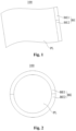
Fig. 1 is a schematic structural view of a display panel according to an embodiment of the present application; -
Fig. 2 is a schematic structural view of another display panel according to an embodiment of the present application; -
Fig. 3 is a schematic structural view of yet another display panel according to an embodiment of the present application; -
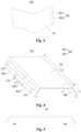
Fig. 4 is a schematic structural view of yet another display panel according to an embodiment of the present application; -
Fig. 5 is a front view of the display panel inFig. 4 ; -
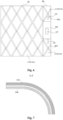
Fig. 6 is a partial schematic structural view of a display panel according to an embodiment of the present application; -
Fig. 7 is a partial cross-sectional view along the line A-A inFig. 4 ; -
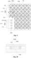
Fig. 8 is a partial schematic structural view of a display panel under a flattened state according to an embodiment of the present application; -
Fig. 9 is a partial schematic structural view of a display panel under a flattened state according to another embodiment of the present application; -
Fig. 10 is a partial cross-sectional view along the line B-B inFig. 9 ; -
Fig. 11 is another partial cross-sectional view along the line A-A inFig. 4 . - An antenna is an important part of an intelligent terminal, and a communication function of the intelligent terminal is realized through the antenna. Under a condition that the antenna is provided, a certain clearance area is required to be ensured, so as to prevent other components from affecting a communication effect of the antenna. However, a large number of antennas are required in 5G communication technology, which is contrary to requirements for a smart terminal such as a smart phone of being light, thin, small and beautiful in design. Due to an insufficient clearance area for the antenna in the mobile phone, the mobile phone communication, especially the high frequency communication, is vulnerable to interference, so that the communication effect is affected. Accordingly, how to arrange more antennas in a relative small mobile phone to improve the communication efficiency of the smart terminal such as the mobile phone is a difficulty.
- Based on this, embodiments of the present application provide a display panel and a display apparatus, so that the technical problem caused by insufficient space for placing an antenna in an intelligent terminal device can be solved.
- With reference to
Fig. 1 to Fig. 7 , thedisplay panel 100 includes a first display area PL and a second display area BE, the second display area BE includes a first area BE1 and a second area BE2 adjacent to each other, afirst antenna 120 is arranged in the first area BE1, and asecond antenna 130 is arranged in the second area BE2. Thedisplay panel 100 further includes touch electrodes arranged in the first display area PL and the second area BE2. - Specifically, relative positions and corresponding shapes of the first display area PL and the second display area BE are different according to differences in shapes of the
display panel 100. - In an example, the first display area PL may be a rectangle, a circle, an oval, and the like in shape. The second display area BE may be provided on the periphery of the first display area PL or may be provided in the first display area PL, which may be selected according to requirements. Under a condition that the second display area BE is provided on the periphery of the first display area PL, the second display area BE may be provided around the entire first display area PL, or may be provided around a part of the periphery of the first display area PL. Optionally, under a condition that the first display area PL is a rectangle in shape, the second display area BE may be provided on one or more sides of the first display area PL.
- Optionally, the first display area PL may be a flat display area or a curved display area, and the second display area BE may also be a flat display area or a curved display area. Specific shapes of the first display area PL and the second display area BE may be selected according to actual requirements.
- In some embodiments, as shown in
Fig. 1 , the first display area PL and the second display area BE may be curved display areas. Under a condition that thecorresponding display panel 100 is applied to a display apparatus, the display apparatus is a curved display apparatus or a flexible display apparatus. In some other embodiments, as shown inFig. 2 , the first display area PL and the second display area BE may be flat display areas. Under a condition that thecorresponding display panel 100 is applied to a display apparatus, the display apparatus is a flat display apparatus. In some embodiments, as shown inFig. 4 , the first display area PL is a flat display area, and the second display area BE is a curved display area, for example, which is formed by bending an edge of the first display area PL. In this way, the object of the present application can still be achieved. - Optionally, the first display area PL may be folded or may not be folded. An example is given in
Fig. 3 to show that the first display area PL of thedisplay panel 100 is folded. - The
display panel 100 may be an organic light emitting diode (OLED)display panel 100 or a liquid crystal display (LCD)display panel 100. - The
first antenna 120 may be a patterned structure, and thesecond antenna 130 may also be a patterned structure, and patterns of thefirst antenna 120 and thesecond antenna 130 may be set according to actual requirements, which is not limited in the present application. -
Touch electrodes 110a are arranged in the second area BE2, that is, the second area BE2 has a touch function. A touch form of the second area BE2 may be self-capacitance or mutual capacitance, and different touch forms correspond to different structural forms of thetouch electrodes 110a. - With reference to
Fig 6 , in some embodiments, the touch form of the second area BE2 is mutual capacitance. Under this condition, thetouch electrodes 110a may be a plurality of electrode blocks arranged on a same layer and distributed in an array, andtouch electrodes 110a in a same matrix row or a same matrix column are electrically connected to each other. - In some other embodiments, the touch form of the second area BE2 is self-capacitance. Under this condition, the
touch electrode 110a includes a touch driving electrode and a touch sensing electrode insulated from each other. One of the touch driving electrode and the touch sensing electrode extends along a row direction, the other of the touch driving electrode and the touch sensing electrode extends along a column direction, and a capacitance can be generated at a position where the two intersect. - With reference to
Fig. 6 , thesecond antennas 130 and thetouch electrodes 110a are arranged in the second area BE2 of the second display area BE, that is, the second area BE2 has both the touch function and the antenna function. Only thefirst antenna 120 is arranged in the first area BE1 of the second display area BE, so that the first area BE1 only has the antenna function, but does not have the touch function. Accordingly, a risk caused by a mis-touch in the first area BE1 to affect the antenna function of the first area BE1 can be reduced, and the first area BE1 has a sufficient space for arranging thefirst antenna 120. - It should be noted that when the second area BE2 samples an antenna signal and a touch signal, the second area BE2 may sample the antenna signal and the touch signal at the same time or alternately. In some embodiments, to avoid mutual interference between two signals, a method of time division multiplexing may be used to sample the antenna signal and the touch signal in the second area BE2.
- Specifically, the antenna signal and the touch signal may be sampled based on a same time period, and as long as a sampling pulse width is narrow enough, a certain time gap will be left between two sampling values of a same signal. Under a condition that a sampling moment of the other signal is exactly in the time gap, sampling values of the two signals do not overlap in time. Optionally, a sampling period of the antenna signal and the touch signal may be set to any value between 1 µs and 10 ms, which may be selected according to specific requirements. The antenna signal and the touch signal are sampled by using the control method, so that the
second antenna 130 and thetouch electrode 110a can share the same space, so as not only to achieve both the antenna function and the touch function for the second area BE2, but also to avoid mutual signal interference caused by performing the alternate collection of the antenna signal and the touch signal. - The
first antenna 120 is arranged in the first area BE1 of the second display area BE, and a position of the first area BE1 in thedisplay panel 100 may be set according to actual situations, so as to achieve a higher screen-to-body ratio for thedisplay panel 100; only thefirst antenna 120 is arranged in the first area BE1, so that the first area BE1 only has a function of receiving or sending a signal, but does not have a touch function. In this way, a sufficient clearance space is provided for thefirst antenna 120, a communication efficiency of thefirst antenna 120 can be improved, and a risk caused by the mis-touch is reduced. In addition, since only thefirst antenna 120 is arranged in the first area BE1, and thetouch electrode 110a is not arranged in the first area BE1, different from the way in which thesecond antenna 130 and thetouch electrode 110a alternately perform the collection of the antenna signal and the touch signal, thefirst antenna 120 can continuously receive and send information, that is, the antenna function can be achieved continuously for thefirst antenna 120. - Optionally, the
first antenna 120 and thesecond antenna 130 may be mi-wave antennas; thefirst antenna 120 may be a main antenna, and thesecond antenna 130 may be an auxiliary antenna, so as to enhance a signal of thefirst antenna 120; under a condition that thesecond antenna 130 is reused as thetouch electrode 110a, thefirst antenna 120, that is, the main antenna, can communicate independently. - In the
display panel 100 according to the embodiments of the present application, thefirst antenna 120 is arranged in the first area BE1 of the second display area BE, thesecond antenna 130 is arranged in the second area BE2 of the second display area BE, and thetouch electrode 110a is also arranged in the second area BE2, that is, the antennas are integrated in the second display area BE of thedisplay panel 100, so that both the display function and the antenna function can be achieved for the second display area BE without providing separate antenna areas, which is not only beneficial for making thedisplay panel 100 light and thin, but also for a high screen-to-body ratio design of thedisplay panel 100. Herein only thefirst antenna 120 is arranged in the first area BE1, so that the space for arranging thefirst antenna 120 is ensured, and a risk caused by the mis-touch in the first area BE1 to affect a function of thefirst antenna 120 can be reduced. In addition, both thesecond antenna 130 and thetouch electrode 110a are arranged in the second area BE2, that is, both the display function and the antenna function can be achieved for the second area BE2. Therefore, while the touch control function of the second area BE2 is not affected, the second area BE2 is reasonably used for better antenna integration design, thereby improving the communication efficiency of thedisplay panel 100. - A number of first areas BE1 and second areas BE2 in the second display area BE may be selected according to requirements. There may be one first area BE1 and one second area BE2, or a plurality of first areas BE1 and a plurality of second areas BE2, and the plurality of first areas BE1 or the plurality of second areas BE2 are distributed alternately. Shapes and sizes of the plurality of first areas BE1 may be same or different, which are set according to actual requirements.
- In some embodiments, the second display area BE is arranged to be a bar in shape and extends along an edge of the first display area PL.
- Specifically, the second display area BE may be a bar in different shapes according to shapes of the edge of the first display area PL. For example, the edge of the first display area PL is an arc in shape, then the second display area BE is a bar in the shape of an arc, and the edge of the second display area PL is a straight line in shape, then the second display area BE is a bar in the shape of a straight line, that is, the second display area BE extends along a straight line.
- Optionally, the second display area BE may be a flat display area or a curved display area.
- The second display area BE is arranged at the edge of the first display area PL, so that the
first antenna 120 and thesecond antenna 130 are integrated in the second display area BE, and thefirst antenna 120 and thesecond antenna 130 are arranged in the second display area BE in the shape of the bar, so that the second display area BE has both the display function and the antenna function. Accordingly, a high screen-to-body ratio is achieved for the display panel. - In some embodiments, along an extending direction X of the second display area BE, the first area BE1 is located in the middle of the corresponding second display area BE, and at least two second areas BE2 are provided respectively at two sides of the first area BE1.
- In an example, one first area BE1 and two second areas BE2 may be provided, the two second areas BE2 are respectively located at two sides of the first area BE1 along the extending direction X. Two first areas BE1 and three second areas BE2 may also be provided, the two first areas BE1 and the three second areas BE2 are distributed alternately along the extending direction X. Of course, more first areas BE1 and more second areas BE2 may also be provided, which may be selected according to specific arrangement requirements.
- Accordingly, the second areas BE2 may be provided at two ends of the second display area BE along the extending direction X, so that performing a touch operation on the second display area BE may be more convenient for an operator.
- In some optional embodiments, an extension length of the second display area BE is L1, and a length of the first area BE1 along the extending direction X of the second display area BE is L2, where 30% ≤ L2/L1 ≤ 50%.
- Specifically, with reference to
Fig. 4 , the second display area BE has one first area BE1 and two second areas BE2 located at two ends of the first area BE1 along the extending direction X. Since the first area BE1 only has the antenna function, and does not have the touch function or is not provided with a touch-related device, and the second area BE2 has the touch function, and a touch operation is not required to be performed on the first area BE1, the first area BE1 is provided at a position close to the middle of the second display area BE, further reducing the risk caused by the mis-touch in the first area BE1. Meanwhile, the second areas BE2 are provided at two ends of the second display area BE along the extending direction X thereof, and since the second area BE2 has the touch function, performing the touch operation on the second display area BE may be more convenient for the operator. - In an example, the first area BE1 is located at the middle of the second display area BE along the extending direction X, and the second areas BE2 at two ends have a same extension length along the extending direction X.
- L2/L1 may be 30%, 35%, 40%, 45%, or 50%, and the like. In an example, the first area BE1 and the second areas BE2 at two ends may divide the second display area BE into three equal sections. Accordingly, the second display area BE can be ensured to have a sufficient space in the first area BE1 for arranging the
first antenna 120, so that a risk caused by an operator's mis-touch in the first area BE1 is reduced, and meanwhile, the second area BE2 has the touch function, so that performing a touch operation on the second areas BE2 of the second display area BE may be more convenient for the operator. - The
first antenna 120, thesecond antenna 130 and thetouch electrode 110a may be arranged on a same layer or on different layers, which may be selected according to specific requirements. In an example, thefirst antenna 120 and thesecond antenna 130 may be arranged on a same layer, and thetouch electrode 110a is arranged on a layer different form the layer on which thefirst antenna 120 and thesecond antenna 130 are arranged. - In some embodiments, the
second antenna 130 and thetouch electrode 110a are arranged on a same layer. - Specifically, with reference to
Fig. 6 and Fig. 7 , thedisplay panel 100 includes abase substrate 140 and atouch layer 110 arranged at a side of thebase substrate 140. Thebase substrate 140 may include a light-emitting structure. Thetouch electrode 110a is arranged on thetouch layer 110. Thesecond antenna 130 is also arranged on thetouch layer 110. With reference toFig. 9 and Fig. 10 , an embodiment is given to show thetouch electrode 110a and thesecond antenna 130 are arranged on a same layer. - According to different touch forms of the second areas BE2, the
display panel 100 may include onetouch layer 110 or a plurality oftouch layers 110,touch electrodes 110a in the second areas BE2 may be arranged in two ormore touch layers 110, andsecond antennas 130 may be arranged in any film layer in the touch layers 110 and is spaced apart from atouch electrode 110a or a lead of the film layer, so as to reduce mutual signal interference. - The
second antenna 130 and thetouch electrode 110a are arranged in the same layer, and a gap betweencorresponding touch electrodes 110a in thetouch layer 110 may be used to arrange thesecond antennas 130, so that the touch function is achieved for the second area BE2 or an electrical signal for achieving the touch function and an antenna function are provided without arranging a separate film layer for thesecond antenna 130, thereby effectively reducing a thickness of thedisplay panel 100. - In an example, under condition that the touch form of the second area BE2 is self-capacitance, the
touch layer 110 includes a touch driving electrode layer and a touch sensing electrode layer insulated from each other, and thesecond antenna 130 may be arranged on the touch driving electrode layer or may also be arranged on the touch sensing electrode layer. - Optionally, the touch form of the second area BE2 may also be mutual capacitance. Under this condition, the
touch layer 110 may include a touch electrode layer and a bridging layer, and thetouch electrode 110a is arranged on the touch electrode layer. Under this condition, thesecond antenna 130 may be arranged on the touch electrode layer. - With the above arrangements, both the touch function and the antenna function can be achieved for the second area BE2 while the thickness of the
display panel 100 is reduced. - In the embodiment where the
second antenna 130 and thetouch electrode 110a are arranged on the same layer, thefirst antenna 120, thesecond antenna 130 and thetouch electrode 110a may be arranged on the same layer, or thefirst antenna 120 may be arranged on a layer different form a layer on which thesecond antenna 130 and thetouch electrode 110a are arranged, so that the antenna function can be achieved for the first area BE1. - In some embodiments, the
first antenna 120 and thetouch electrode 110a are arranged on the same layer. That is, thefirst antenna 120, thesecond antenna 130, and thetouch electrode 110a are arranged on thetouch layer 110, thereby further reducing the thickness of thedisplay panel 100. - Specifically, the
touch electrodes 110a are arranged in the first display area PL and in the second area BE2, and thefirst antenna 120 and thesecond antenna 130 are arranged in the second display area BE, then a film layer of the second display area BE and a film layer corresponding to the first display area PL can be formed together. Accordingly, the thickness of thedisplay panel 100 may be further reduced. - In some other embodiments, the
display panel 100 includes atouch layer 110 and an antenna layer arranged in a stack, thetouch electrode 110a is arranged on the touch layer, and thesecond antenna 130 is arranged on the antenna layer. - That is, the
touch electrode 110a and thesecond antenna 130 are arranged in different layers, or may be located in adjacent film layers or may be spaced apart by one or more film layers. - The
touch electrode 110a and thesecond antenna 130 are arranged on different film layers, so that a difficulty for processing thedisplay panel 100 can be reduced, and a risk caused by short circuit of thesecond antenna 130 and thetouch electrode 110a is reduced. - In some embodiments, as shown in
Fig. 8 , thefirst antenna 120 includes at least onefirst antenna unit 121, and thesecond antenna 130 includes one or moresecond antenna units 131. - Optionally, a structure may be reused by the
second antenna unit 131 and thetouch electrode 110a in the second area BE2, or structures may be provided for thesecond antenna unit 131 and thetouch electrode 110a, respectively. - Specifically, the
first antenna 120 may be connected to afirst antenna terminal 173 through afirst wiring 171. - In some embodiments, at least a part of the
touch electrodes 110a in the second area BE2 are reused as thesecond antenna unit 131. - The structure reused as the
touch electrode 110a of thesecond antenna unit 131 may be connected to asecond antenna terminal 174 through asecond wiring 172. Since the method of time division multiplexing may be used to sample the touch signal and the antenna signal in the second area BE2 respectively, a structure reused by thetouch electrode 110a and thesecond antenna unit 131 does not cause signal interference, and can further simplify a structure of thedisplay panel 100. Optionally, thedisplay panel 100 further includes a touch binding terminal, and thetouch electrode 110a is connected to the touch binding terminal through a touch wiring, which is not described in detail. - In some other embodiments, as shown in
Fig. 9 and Fig. 10 , thesecond antenna 130 includes thesecond antenna unit 131, and thesecond antenna unit 131 is spaced apart from thetouch electrode 110a, which specifically means that thesecond antenna unit 131 is spaced apart and insulated from a conductive material forming thetouch electrode 110a. - In an example, the touch form of the
display panel 100 is mutual capacitance, a plurality oftouch electrodes 110a are distributed on a same layer in an array, and thetouch electrodes 110a in a same matrix row or in a same matrix column are electrically connected to each other. One ofsecond antenna units 131 or a plurality ofsecond antenna units 131 are electrically connected to form an antenna pattern to achieve a corresponding antenna function. Thesecond antenna unit 131 and thetouch electrode 110a are spaced apart from each other, then thesecond antenna unit 131 and thetouch electrode 110a do not conduct electricity to each other, and thus do not cause signal interference with each other. Accordingly, both the touch function and the antenna function are achieved for the second area BE2 while the thickness of thedisplay panel 100 is further reduced. - The
second antenna unit 131 may be arranged between twoadjacent touch electrodes 110a, thesecond antenna unit 131 may be arranged around thetouch electrodes 110a, or thetouch electrode 110a may be arranged around thesecond antenna unit 131. - In some optional embodiments, with further reference to
Fig. 9 and Fig. 10 , at least a part of thetouch electrodes 110a are arranged around thesecond antenna unit 131. - Specifically, the
second antenna units 131 are distributed in one row or one column, or thesecond antenna units 131 are distributed in a matrix, and at least a part of thetouch electrodes 110a are arranged around thesecond antenna unit 131, that is, thesecond antenna unit 131 is arranged incorresponding touch electrode 110a. - A portion of the
touch electrodes 110a are arranged around thesecond antenna unit 131, so that a distribution pattern of thetouch electrode 110a is not disturbed while the thickness of thedisplay panel 100 is reduced, so as to ensure a touch sensitivity of the second area BE2. - The
first antenna 120 and thesecond antenna 130 may respectively be a long-wave antenna, a medium-wave antenna, a short-wave antenna, an ultra-short-wave antenna or a microwave antenna, which may be selected according to actual requirements. - In some embodiments, the
first antenna 120 and thesecond antenna 130 are millimeter-wave antennas, thefirst antenna 120 is the main antenna, and thesecond antenna 130 is the auxiliary antenna and used to enhance the signal of the first antenna. - Specifically, the function achieved by the
first antenna 120 and thesecond antenna 130 is same, and thesecond antenna 130 may increase an efficiency of transmitting the signal by thefirst antenna 120, so that the corresponding antenna function has a better effect. - In some other embodiments, the
first antenna 120 and thesecond antenna 130 may be non-millimeter-wave antennas, and thefirst antenna 120 and thesecond antenna 130 may specifically constitute one or more of antennas used in Bluetooth, Wireless Network Communication Technology (Wi-Fi), a Global Positioning System (GPS), Near Field Communication (NFC), and a laser-direct-structuring (LDS). - In some embodiments, the
first antenna 120 is an NFC antenna. That is, a near field communication function of the display apparatus is achieved by thefirst antenna 120. - The
second antenna 130 and thefirst antenna 120 may be a same type of antennas, or may be different types of antennas, which may be set according to actual requirements. - In some embodiments, the
second antenna 130 is a NFC antenna. That is, a near field communication signal of thedisplay panel 100 is enhanced by thesecond antenna 130, so that a near field communication efficiency of thedisplay panel 100 is increased. - In some embodiments, the
display panel 100 further includes an antenna layer, and thefirst antenna 120 and/or thesecond antenna 130 are/is arranged on the antenna layer. - That is, at least one of the
first antenna 120 and thesecond antenna 130 is arranged on the antenna layer, the other of thefirst antenna 120 and thesecond antenna 130 is arranged on another film layer, or both thefirst antenna 120 and thesecond antenna 130 are arranged on the antenna layer. - There may be one antenna layer or a plurality of antenna layers. Under a condition that there is one antenna layer, both the
first antenna 120 and thesecond antenna 130 may be arranged on the antenna layer, or one of thefirst antenna 120 and thesecond antenna 130 may be arranged on the antenna layer. Under a condition that there are the plurality of antenna layers, thefirst antenna 120 and thesecond antenna 130 may be arranged on different antenna layers or may be arranged on a same antenna layer. - The antenna layer is arranged to facilitate the arrangement of a corresponding
first antenna 120 and/or a correspondingsecond antenna 130, thereby reducing the difficulty for processing thedisplay panel 100. - In some embodiments, as shown in
Fig. 4 andFig. 11 , thedisplay panel 100 includes thebase substrate 140, a light-emitting layer and apolarizing layer 150 arranged in sequence at a side of thebase substrate 140, and thefirst antenna 120 is arranged on thepolarizing layer 150. - That is, the
first antenna 120 is integrated in thepolarizing layer 150 without providing a separate film layer, thereby further reducing the thickness of thedisplay panel 100. In the solution that thefirst antenna 120 is arranged on thepolarizing layer 150, a signal interference between thefirst antenna 120 and other film layer-related components can be reduced, and the communication efficiency of thedisplay panel 100 is improved. - In the embodiment that the
first antenna 120 is arranged on thepolarizing layer 150, thesecond antenna 130 may be arranged on thepolarizing layer 150, or may be arranged on other film layers, which may be set according to actual requirements. - In some embodiments, the
second antenna 130 is arranged on thepolarizing layer 150. As such, thefirst antenna 120 and thesecond antenna 130 are integrated in a same film layer, thereby further reducing the thickness of thedisplay panel 100. - In some embodiments, with further reference to
Fig. 4 andFig. 11 , thedisplay panel 100 includes thebase substrate 140, a light-emitting layer and anencapsulation layer 160 arranged in sequence at a side of thebase substrate 140, and thefirst antenna 120 is arranged on theencapsulation layer 160. - That is, in addition to integrating the
first antenna 120 in thepolarizing layer 150, thefirst antenna 120 may also be integrated in theencapsulation layer 160 without providing a separate film layer, so that the thickness of thedisplay panel 100 can still be reduced. In the solution that thefirst antenna 120 is arranged on theencapsulation layer 160, a signal interference between thefirst antenna 120 and other film layer-related components can still be reduced, and the communication efficiency of thedisplay panel 100 is improved. - In some embodiments, the
second antenna 130 is arranged on theencapsulation layer 160. As such, a thickness of the film layers of thedisplay panel 100 can be reduced. - In an embodiment that the
display panel 100 includes both thepolarizing layer 150 and theencapsulation layer 160, thepolarizing layer 150 is arranged at a side of thebase substrate 140, and theencapsulation layer 160 is arranged at a side of thepolarizing layer 150 away from thebase substrate 140. Under this condition, thefirst antenna 120 and thesecond antenna 130 may be arranged on theencapsulation layer 160, or may be arranged on thepolarizing layer 150, or one of thefirst antenna 120 and thesecond antenna 130 may be arranged on theencapsulation layer 160 and the other of thefirst antenna 120 and thesecond antenna 130 may be arranged on thepolarizing layer 150, which may be selected according to actual requirements. - The
polarizing layer 150 is arranged at a side of thebase substrate 140, this does not mean that thepolarizing layer 150 is arranged directly on a surface of thebase substrate 140, instead it means that other film layers may be arranged between thepolarizing layer 150 and thebase substrate 140. Other film layers may further be arranged between theencapsulation layer 160 and thepolarizing layer 150. - In some embodiments, with further reference to
Fig. 4 andFig. 11 , thedisplay panel 100 includes anarray substrate 170 and a light-emitting layer arranged in sequence at a side of thebase substrate 140, and thefirst antenna 120 and/or thesecond antenna 130 are/is arranged on thearray substrate 170. That is, at least one of thefirst antenna 120 and thesecond antenna 130 is integrated in thearray substrate 170 of thedisplay panel 100, so that the purpose of reducing the thickness of thedisplay panel 100 can still be achieved. - In some embodiments, the
array substrate 170 includes a metal layer, and thefirst antenna 120 and/or thesecond antenna 130 are/is arranged on the metal layer. That is, at least one of thefirst antenna 120 and thesecond antenna 130 is arranged on the metal layer. Thearray substrate 170 includes at least two metal layers, and thefirst antenna 120 and thesecond antenna 130 may be arranged on a same metal layer or different metal layers. - According to differences in the structure of the
display panel 100, one second display area BE may be arranged in thedisplay panel 100, or a plurality of second display areas BE may be arranged in thedisplay panel 100. In an embodiment that the plurality of second display areas BE are arranged in thedisplay panel 100, the plurality of second display areas BE may be adjacent to each other or may be spaced apart from each other. In an example, two second display areas BE of thedisplay panel 100 are arranged at two sides of the first display area PL opposing to each other, that is, the two second display areas BE are arranged in parallel. - In an embodiment that the plurality of second display areas BE are arranged in the
display panel 100, thefirst antenna 120 and thesecond antenna 130 may be arranged in each second display area BE, or thefirst antenna 120 and thesecond antenna 130 may be arranged in a portion of the second display areas BE, which may be selected according to specific requirements. - In some embodiments, the
display panel 100 includes at least two second display areas BE, and the first area BE1 and the second area BE2 are arranged in at least one of the second display areas BE. - Specifically, the at least one of the second display areas BE includes the first area BE1 and the second area BE2, the
first antenna 120 is arranged in the first area BE1, and thesecond antenna 130 and thetouch electrode 110a are arranged in the second area BE2. Other second display areas BE may only have the display function, or may have both the display function and the touch function. - The
first antennas 120 and thesecond antennas 130 are arranged in at least one second display area BE, and thefirst antennas 120 and thesecond antennas 130 may be arranged in the plurality of second display areas BE according to actual requirements, so that a sufficient space is provided for arranging thefirst antennas 120 and thesecond antennas 130, and the communication efficiency of thedisplay panel 100 is further improved. - As shown in
Fig. 4 , in some embodiments, the first display area PL is the flat display area, and the second display area BE is the bent display area. - Specifically, after the bent display area is integrated with the flat display area, the bent display area may be formed by bending an edge of the flat display area, and the
first antenna 120 and thesecond antenna 130 are arranged in the bent display area. Thefirst antenna 120 and thesecond antenna 130 are arranged respectively based on a position of the bent display area without occupying a position and a space of the flat display area or a non-display area, which is beneficial for improving the screen-to-body ratio of thedisplay panel 100. - In some embodiments, the
display panel 100 includes at least two bent display areas, and the first area BE1 and the second area BE2 are arranged in at least one of the at least two bent display areas. That is, the first area BE1 and the second area BE2 may be formed in one bent display area, and of course, may be formed in different bent display areas, respectively. As such, positions of thefirst antenna 120 and thesecond antenna 130 can be appropriately provided according to actual requirements. - The display apparatus according to the embodiments of the present application includes the
display panel 100 according to any of the above embodiments. - Due to the use of the
display panel 100 according to any of the above embodiments, the display apparatus according to the embodiments of the present application has the same technical effect, which is not repeated here.
Claims (19)
- A display panel comprising:a first display area;a second display area comprising a first area and at least one second area adjacent to each other;a first antenna arranged in the first area;a second antenna arranged in the at least one second area; anda plurality of touch electrodes arranged in the first display area and the at least one second area.
- The display panel according to claim 1, wherein the second display area is arranged to be a bar in shape and extends along an edge of the first display area.
- The display panel according to claim 2, wherein the second display area extends along a straight line.
- The display panel according to claim 2, wherein the at least one second area comprises at least two second areas, and along an extending direction of the second display area, the first area is located in the middle of the corresponding second display area, and the at least two second areas are respectively provided at two sides of the first area.
- The display panel according to any of claims 2 to 4, wherein an extension length of the second display area is L1, and an extension length of the first area along the extending direction of the second display area is L2, wherein 30% ≤ L2/L1 ≤ 50%.
- The display panel according to claim 1, wherein the second antenna and the touch electrodes are arranged in a same layer.
- The display panel according to claim 1, wherein the first antenna and the touch electrodes are arranged in a same layer.
- The display panel according to claim 1 or 6, wherein the first antenna comprises a first antenna unit; the second antenna comprises a second antenna unit, and at least a part of the touch electrodes in the at least one second area are reused as the second antenna unit; or, at least a part of the touch electrodes are arranged around the second antenna unit.
- The display panel according to claim 1, wherein the first antenna and the second antenna are millimeter-wave antennas; the first antenna is a main antenna, and the second antenna is an auxiliary antenna to enhance a signal of the first antenna.
- The display panel according to claim 1, wherein the first antenna is one or more of a Bluetooth antenna, a wireless network communication technology antenna, a global positioning system antenna, a near field communication antenna and a laser-direct-structuring antenna; and the second antenna is one or more of a Bluetooth antenna, a wireless network communication technology antenna, a global positioning system antenna, a near field communication antenna and a laser-direct-structuring antenna.
- The display panel according to claim 1, further comprising an antenna layer, wherein at least one of the first antenna and the second antenna are arranged in the antenna layer.
- The display panel according to claim 1, further comprising a base substrate, and a light-emitting layer and a polarizing layer arranged in sequence at a side of the base substrate, wherein at least one of the first antenna and the second antenna are arranged in the polarizing layer.
- The display panel according to claim 1, further comprising a base substrate, and a light-emitting layer and an encapsulation layer arranged in sequence at a side of the base substrate, wherein at least one of the first antenna and the second antenna are arranged in the encapsulation layer.
- The display panel according to claim 1, wherein the display panel comprises a base substrate, and an array substrate and a light-emitting layer arranged in sequence at a side of the base substrate, wherein at least one of the first antenna and the second antenna are arranged on the array substrate.
- The display panel according to claim 14, wherein the array substrate comprises a metal layer, and at least one of the first antenna and the second antenna are arranged in the metal layer.
- The display panel according to claim 1, wherein the display panel comprises at least two second display areas, and the first area and the at least one second area are provided in at least one of the second display areas.
- The display panel according to claim 1, wherein the first display area is a flat display area, and the second display area is a bent display area.
- The display panel according to claim 17, wherein the display panel comprises at least two bent display areas, the first area and the at least one second area are provided in at least one of the bent display areas.
- A display apparatus comprising the display panel according to any of claims 1 to 18.
Applications Claiming Priority (3)
| Application Number | Priority Date | Filing Date | Title |
|---|---|---|---|
| CN202111607714 | 2021-12-27 | ||
| CN202210286830.XA CN114553993B (en) | 2021-12-27 | 2022-03-23 | Display panel and display device |
| PCT/CN2022/113694 WO2023124131A1 (en) | 2021-12-27 | 2022-08-19 | Display panel and display apparatus |
Publications (2)
| Publication Number | Publication Date |
|---|---|
| EP4459962A1 true EP4459962A1 (en) | 2024-11-06 |
| EP4459962A4 EP4459962A4 (en) | 2025-03-26 |
Family
ID=81665699
Family Applications (1)
| Application Number | Title | Priority Date | Filing Date |
|---|---|---|---|
| EP22913415.0A Pending EP4459962A4 (en) | 2021-12-27 | 2022-08-19 | SCOREBOARD AND DISPLAY DEVICE |
Country Status (7)
| Country | Link |
|---|---|
| US (1) | US12614836B2 (en) |
| EP (1) | EP4459962A4 (en) |
| JP (1) | JP7634725B2 (en) |
| KR (1) | KR20230155015A (en) |
| CN (1) | CN114553993B (en) |
| TW (1) | TWI825968B (en) |
| WO (1) | WO2023124131A1 (en) |
Families Citing this family (3)
| Publication number | Priority date | Publication date | Assignee | Title |
|---|---|---|---|---|
| CN114553993B (en) * | 2021-12-27 | 2025-07-15 | 云谷(固安)科技有限公司 | Display panel and display device |
| CN115498413B (en) * | 2022-09-02 | 2026-05-08 | 苏州国显创新科技有限公司 | A display panel and display device |
| CN115576445B (en) * | 2022-09-30 | 2026-03-06 | 维沃移动通信有限公司 | Touch display devices and electronic devices |
Family Cites Families (43)
| Publication number | Priority date | Publication date | Assignee | Title |
|---|---|---|---|---|
| JP3959332B2 (en) | 2001-10-24 | 2007-08-15 | 松下電器産業株式会社 | Portable wireless terminal |
| CN102591521B (en) | 2011-01-11 | 2016-03-23 | 富士康(昆山)电脑接插件有限公司 | Touch screen device and manufacture method thereof |
| CN102882545B (en) | 2012-09-21 | 2015-08-05 | 敦泰科技有限公司 | Communication equipment |
| TW201435670A (en) * | 2013-03-08 | 2014-09-16 | Wintek Corp | Touch display apparatus |
| KR101504237B1 (en) | 2013-11-15 | 2015-03-19 | 엘지전자 주식회사 | Mobile terminal and method of controlling the mobile terminal |
| CN203720722U (en) | 2014-01-30 | 2014-07-16 | 宇龙计算机通信科技(深圳)有限公司 | Display screen integrating function of antennae and terminal equipment applying display screen |
| KR102316228B1 (en) * | 2015-04-01 | 2021-10-25 | 오상진 | Antenna-Integrated Touch Detection Apparatus And Manufacturing Method Thereof |
| TWI792916B (en) | 2016-06-24 | 2023-02-11 | 日商半導體能源研究所股份有限公司 | display device, electronic device |
| KR102725327B1 (en) * | 2016-12-30 | 2024-11-01 | 엘지디스플레이 주식회사 | Antenna Integrated Polarizer and Flexible Display Device Using the Same |
| KR102009382B1 (en) * | 2017-03-03 | 2019-08-09 | 동우 화인켐 주식회사 | Touch sensor equipped with antenna |
| CN108279737A (en) | 2018-01-19 | 2018-07-13 | 云谷(固安)科技有限公司 | Display screen and display device |
| KR102514547B1 (en) | 2018-07-16 | 2023-03-27 | 삼성전자주식회사 | Display assembly including antenna and electronic device with the same |
| KR102190667B1 (en) * | 2018-10-05 | 2020-12-14 | 동우 화인켐 주식회사 | Touch sensor-antenna module and display device including the same |
| KR102671154B1 (en) | 2018-12-31 | 2024-05-30 | 엘지디스플레이 주식회사 | Display apparatus with integrated antenna |
| US11275473B2 (en) | 2019-06-13 | 2022-03-15 | Samsung Display Co., Ltd. | Display panel and display device including the same |
| KR102099830B1 (en) * | 2019-06-17 | 2020-04-10 | 동우 화인켐 주식회사 | Antenna-combined module and display device including the same |
| CN112215215B (en) | 2019-07-12 | 2025-01-03 | 群创光电股份有限公司 | Electronic Devices |
| CN112306273A (en) * | 2019-07-26 | 2021-02-02 | 北京小米移动软件有限公司 | Touch display screen and mobile terminal |
| CN210270841U (en) * | 2019-08-05 | 2020-04-07 | 维沃移动通信有限公司 | A display panel and terminal equipment |
| CN210270842U (en) * | 2019-08-05 | 2020-04-07 | 维沃移动通信有限公司 | Display panel and terminal equipment |
| CN112578925B (en) * | 2019-09-29 | 2022-07-19 | 昆山国显光电有限公司 | Touch display panel and touch display device |
| CN112578926A (en) * | 2019-09-29 | 2021-03-30 | 昆山国显光电有限公司 | Touch layer group, touch display panel and touch terminal |
| KR20210041156A (en) * | 2019-10-04 | 2021-04-15 | 삼성디스플레이 주식회사 | Display apparatus and electric apparatus having the same |
| KR102915058B1 (en) * | 2019-10-08 | 2026-01-21 | 삼성디스플레이 주식회사 | Display apparatus |
| KR102805061B1 (en) * | 2019-10-31 | 2025-05-12 | 삼성디스플레이 주식회사 | Display apparatus |
| CN210489811U (en) * | 2019-11-21 | 2020-05-08 | 维沃移动通信有限公司 | Electronic equipment |
| CN112947780A (en) * | 2019-11-26 | 2021-06-11 | 南昌欧菲光科技有限公司 | Touch screen, touch display and electronic equipment |
| KR102878855B1 (en) * | 2019-12-31 | 2025-10-30 | 엘지디스플레이 주식회사 | Touch display device |
| CN113131179A (en) | 2020-01-15 | 2021-07-16 | 钉钉控股(开曼)有限公司 | Communication equipment, Internet of things equipment and communication method |
| WO2021151483A1 (en) * | 2020-01-29 | 2021-08-05 | Huawei Technologies Co., Ltd. | Display stack with millimeter-wave antenna functionality |
| KR102819577B1 (en) | 2020-02-26 | 2025-06-12 | 삼성디스플레이 주식회사 | Display device |
| CN111367435B (en) * | 2020-03-17 | 2024-06-04 | 京东方科技集团股份有限公司 | Display panel and display device |
| KR102736356B1 (en) * | 2020-03-23 | 2024-12-02 | 삼성디스플레이 주식회사 | Electric device and communication method |
| KR102684573B1 (en) * | 2020-04-21 | 2024-07-16 | 삼성디스플레이 주식회사 | Electronic device |
| KR102942511B1 (en) * | 2020-05-13 | 2026-03-24 | 삼성디스플레이 주식회사 | Display device |
| CN111857430B (en) * | 2020-07-22 | 2024-01-30 | 京东方科技集团股份有限公司 | Display panel and display device |
| CN112612323B (en) * | 2020-12-28 | 2024-06-25 | 维沃移动通信有限公司 | Display modules and electronic devices |
| CN112864204B (en) * | 2021-01-13 | 2024-06-28 | 京东方科技集团股份有限公司 | A display panel, a touch detection method thereof and a display device |
| CN112764583B (en) * | 2021-01-27 | 2025-02-25 | 维沃移动通信有限公司 | Touch screen and electronic devices |
| CN112882572A (en) * | 2021-02-03 | 2021-06-01 | 维沃移动通信有限公司 | Touch panel, electronic equipment and control method of working state |
| CN113035924A (en) * | 2021-03-09 | 2021-06-25 | 京东方科技集团股份有限公司 | Display panel and display device |
| CN113296635B (en) * | 2021-05-31 | 2022-07-12 | 武汉华星光电半导体显示技术有限公司 | Touch display panel and display device |
| CN114553993B (en) * | 2021-12-27 | 2025-07-15 | 云谷(固安)科技有限公司 | Display panel and display device |
-
2022
- 2022-03-23 CN CN202210286830.XA patent/CN114553993B/en active Active
- 2022-08-19 EP EP22913415.0A patent/EP4459962A4/en active Pending
- 2022-08-19 WO PCT/CN2022/113694 patent/WO2023124131A1/en not_active Ceased
- 2022-08-19 JP JP2023566726A patent/JP7634725B2/en active Active
- 2022-08-19 KR KR1020237036258A patent/KR20230155015A/en active Pending
- 2022-09-01 TW TW111133225A patent/TWI825968B/en active
-
2023
- 2023-10-30 US US18/497,200 patent/US12614836B2/en active Active
Also Published As
| Publication number | Publication date |
|---|---|
| TW202301092A (en) | 2023-01-01 |
| KR20230155015A (en) | 2023-11-09 |
| US12614836B2 (en) | 2026-04-28 |
| JP7634725B2 (en) | 2025-02-21 |
| CN114553993A (en) | 2022-05-27 |
| TWI825968B (en) | 2023-12-11 |
| CN114553993B (en) | 2025-07-15 |
| JP2024519475A (en) | 2024-05-14 |
| US20240063529A1 (en) | 2024-02-22 |
| EP4459962A4 (en) | 2025-03-26 |
| WO2023124131A1 (en) | 2023-07-06 |
Similar Documents
| Publication | Publication Date | Title |
|---|---|---|
| US12614836B2 (en) | Display panel and display apparatus | |
| CN114628886B (en) | Electronic device with probe-fed dielectric resonator antenna | |
| CN113540773B (en) | Electronic device with compact ultra wideband antenna | |
| KR20210001976A (en) | Electronic devices having multi-frequency ultra-wideband antennas | |
| US10763574B2 (en) | Display device, color filter substrate, mobile terminal and driving method thereof | |
| CN111193110B (en) | Antenna devices and electronic equipment | |
| CN102593578B (en) | Coupling feed-in type antenna device for mobile phone | |
| US10944153B1 (en) | Electronic devices having multi-band antenna structures | |
| EP4333204A1 (en) | Display apparatus and electronic device | |
| CN106940605B (en) | Display panel | |
| CN108398822B (en) | Touch display substrate, display panel and display device | |
| CN111596481B (en) | Display panel, display device and manufacturing method | |
| TW201208511A (en) | PCB antenna layout | |
| KR102443597B1 (en) | A wireless communication structure, a display panel and a wireless communication device | |
| US20140028619A1 (en) | Touch Sensitive Apparatus, Mobile Terminal And Terminal Device | |
| CN112612374A (en) | Display module and electronic equipment | |
| CN112732112A (en) | Display module and electronic equipment | |
| EP3920322A1 (en) | Antenna apparatus and electronic device | |
| CN112310622A (en) | Antenna devices and electronic equipment | |
| EP4266497A1 (en) | Electronic device | |
| CN108987943B (en) | Millimeter wave wireless terminal equipment | |
| CN102347527A (en) | Antenna device and mobile device | |
| CN112578928A (en) | Touch module and touch display panel | |
| US20220293697A1 (en) | Display panel and display device | |
| CN111725611B (en) | Dual-frequency antenna structure and display panel |
Legal Events
| Date | Code | Title | Description |
|---|---|---|---|
| STAA | Information on the status of an ep patent application or granted ep patent |
Free format text: STATUS: THE INTERNATIONAL PUBLICATION HAS BEEN MADE |
|
| PUAI | Public reference made under article 153(3) epc to a published international application that has entered the european phase |
Free format text: ORIGINAL CODE: 0009012 |
|
| STAA | Information on the status of an ep patent application or granted ep patent |
Free format text: STATUS: REQUEST FOR EXAMINATION WAS MADE |
|
| 17P | Request for examination filed |
Effective date: 20231030 |
|
| AK | Designated contracting states |
Kind code of ref document: A1 Designated state(s): AL AT BE BG CH CY CZ DE DK EE ES FI FR GB GR HR HU IE IS IT LI LT LU LV MC MK MT NL NO PL PT RO RS SE SI SK SM TR |
|
| A4 | Supplementary search report drawn up and despatched |
Effective date: 20250226 |
|
| RIC1 | Information provided on ipc code assigned before grant |
Ipc: H01Q 1/38 20060101ALI20250220BHEP Ipc: H01Q 1/22 20060101ALI20250220BHEP Ipc: G06F 3/041 20060101ALI20250220BHEP Ipc: H04M 1/02 20060101AFI20250220BHEP |
|
| DAV | Request for validation of the european patent (deleted) | ||
| DAX | Request for extension of the european patent (deleted) | ||
| RAP1 | Party data changed (applicant data changed or rights of an application transferred) |
Owner name: SUZHOU GOVISIONOX INNOVATION TECHNOLOGY CO., LTD. |