EP4459443A1 - Haptic rendering display panel and display device - Google Patents
Haptic rendering display panel and display device Download PDFInfo
- Publication number
- EP4459443A1 EP4459443A1 EP22939219.6A EP22939219A EP4459443A1 EP 4459443 A1 EP4459443 A1 EP 4459443A1 EP 22939219 A EP22939219 A EP 22939219A EP 4459443 A1 EP4459443 A1 EP 4459443A1
- Authority
- EP
- European Patent Office
- Prior art keywords
- display panel
- piezoelectric vibration
- vibration devices
- base substrate
- tactile reproduction
- Prior art date
- Legal status (The legal status is an assumption and is not a legal conclusion. Google has not performed a legal analysis and makes no representation as to the accuracy of the status listed.)
- Granted
Links
Images



Classifications
-
- G—PHYSICS
- G06—COMPUTING OR CALCULATING; COUNTING
- G06F—ELECTRIC DIGITAL DATA PROCESSING
- G06F3/00—Input arrangements for transferring data to be processed into a form capable of being handled by the computer; Output arrangements for transferring data from processing unit to output unit, e.g. interface arrangements
- G06F3/01—Input arrangements or combined input and output arrangements for interaction between user and computer
- G06F3/03—Arrangements for converting the position or the displacement of a member into a coded form
- G06F3/041—Digitisers, e.g. for touch screens or touch pads, characterised by the transducing means
-
- G—PHYSICS
- G06—COMPUTING OR CALCULATING; COUNTING
- G06F—ELECTRIC DIGITAL DATA PROCESSING
- G06F3/00—Input arrangements for transferring data to be processed into a form capable of being handled by the computer; Output arrangements for transferring data from processing unit to output unit, e.g. interface arrangements
- G06F3/01—Input arrangements or combined input and output arrangements for interaction between user and computer
- G06F3/016—Input arrangements with force or tactile feedback as computer generated output to the user
-
- G—PHYSICS
- G02—OPTICS
- G02F—OPTICAL DEVICES OR ARRANGEMENTS FOR THE CONTROL OF LIGHT BY MODIFICATION OF THE OPTICAL PROPERTIES OF THE MEDIA OF THE ELEMENTS INVOLVED THEREIN; NON-LINEAR OPTICS; FREQUENCY-CHANGING OF LIGHT; OPTICAL LOGIC ELEMENTS; OPTICAL ANALOGUE/DIGITAL CONVERTERS
- G02F1/00—Devices or arrangements for the control of the intensity, colour, phase, polarisation or direction of light arriving from an independent light source, e.g. switching, gating or modulating; Non-linear optics
- G02F1/01—Devices or arrangements for the control of the intensity, colour, phase, polarisation or direction of light arriving from an independent light source, e.g. switching, gating or modulating; Non-linear optics for the control of the intensity, phase, polarisation or colour
- G02F1/13—Devices or arrangements for the control of the intensity, colour, phase, polarisation or direction of light arriving from an independent light source, e.g. switching, gating or modulating; Non-linear optics for the control of the intensity, phase, polarisation or colour based on liquid crystals, e.g. single liquid crystal display cells
- G02F1/133—Constructional arrangements; Operation of liquid crystal cells; Circuit arrangements
- G02F1/1333—Constructional arrangements; Manufacturing methods
- G02F1/13338—Input devices, e.g. touch panels
-
- G—PHYSICS
- G02—OPTICS
- G02F—OPTICAL DEVICES OR ARRANGEMENTS FOR THE CONTROL OF LIGHT BY MODIFICATION OF THE OPTICAL PROPERTIES OF THE MEDIA OF THE ELEMENTS INVOLVED THEREIN; NON-LINEAR OPTICS; FREQUENCY-CHANGING OF LIGHT; OPTICAL LOGIC ELEMENTS; OPTICAL ANALOGUE/DIGITAL CONVERTERS
- G02F1/00—Devices or arrangements for the control of the intensity, colour, phase, polarisation or direction of light arriving from an independent light source, e.g. switching, gating or modulating; Non-linear optics
- G02F1/01—Devices or arrangements for the control of the intensity, colour, phase, polarisation or direction of light arriving from an independent light source, e.g. switching, gating or modulating; Non-linear optics for the control of the intensity, phase, polarisation or colour
- G02F1/13—Devices or arrangements for the control of the intensity, colour, phase, polarisation or direction of light arriving from an independent light source, e.g. switching, gating or modulating; Non-linear optics for the control of the intensity, phase, polarisation or colour based on liquid crystals, e.g. single liquid crystal display cells
- G02F1/133—Constructional arrangements; Operation of liquid crystal cells; Circuit arrangements
- G02F1/1333—Constructional arrangements; Manufacturing methods
- G02F1/133388—Constructional arrangements; Manufacturing methods with constructional differences between the display region and the peripheral region
-
- G—PHYSICS
- G06—COMPUTING OR CALCULATING; COUNTING
- G06F—ELECTRIC DIGITAL DATA PROCESSING
- G06F3/00—Input arrangements for transferring data to be processed into a form capable of being handled by the computer; Output arrangements for transferring data from processing unit to output unit, e.g. interface arrangements
- G06F3/01—Input arrangements or combined input and output arrangements for interaction between user and computer
-
- G—PHYSICS
- G06—COMPUTING OR CALCULATING; COUNTING
- G06F—ELECTRIC DIGITAL DATA PROCESSING
- G06F3/00—Input arrangements for transferring data to be processed into a form capable of being handled by the computer; Output arrangements for transferring data from processing unit to output unit, e.g. interface arrangements
- G06F3/01—Input arrangements or combined input and output arrangements for interaction between user and computer
- G06F3/03—Arrangements for converting the position or the displacement of a member into a coded form
- G06F3/041—Digitisers, e.g. for touch screens or touch pads, characterised by the transducing means
- G06F3/044—Digitisers, e.g. for touch screens or touch pads, characterised by the transducing means by capacitive means
- G06F3/0443—Digitisers, e.g. for touch screens or touch pads, characterised by the transducing means by capacitive means using a single layer of sensing electrodes
-
- G—PHYSICS
- G06—COMPUTING OR CALCULATING; COUNTING
- G06F—ELECTRIC DIGITAL DATA PROCESSING
- G06F3/00—Input arrangements for transferring data to be processed into a form capable of being handled by the computer; Output arrangements for transferring data from processing unit to output unit, e.g. interface arrangements
- G06F3/01—Input arrangements or combined input and output arrangements for interaction between user and computer
- G06F3/03—Arrangements for converting the position or the displacement of a member into a coded form
- G06F3/041—Digitisers, e.g. for touch screens or touch pads, characterised by the transducing means
- G06F3/044—Digitisers, e.g. for touch screens or touch pads, characterised by the transducing means by capacitive means
- G06F3/0446—Digitisers, e.g. for touch screens or touch pads, characterised by the transducing means by capacitive means using a grid-like structure of electrodes in at least two directions, e.g. using row and column electrodes
-
- G—PHYSICS
- G06—COMPUTING OR CALCULATING; COUNTING
- G06F—ELECTRIC DIGITAL DATA PROCESSING
- G06F3/00—Input arrangements for transferring data to be processed into a form capable of being handled by the computer; Output arrangements for transferring data from processing unit to output unit, e.g. interface arrangements
- G06F3/01—Input arrangements or combined input and output arrangements for interaction between user and computer
- G06F3/03—Arrangements for converting the position or the displacement of a member into a coded form
- G06F3/041—Digitisers, e.g. for touch screens or touch pads, characterised by the transducing means
- G06F3/044—Digitisers, e.g. for touch screens or touch pads, characterised by the transducing means by capacitive means
- G06F3/0447—Position sensing using the local deformation of sensor cells
Definitions
- Embodiments of the present disclosure relate to a tactile reproduction display panel and a display apparatus.
- Haptics is the focus of current technology development, the concept of Haptics is that with the help of haptic technology, electronic equipment manufacturers can create distinctive personalized haptic feedback for specific interactive experiences on their devices, thus providing consumers with more valuable and realistic unique experiences.
- Haptics can be divided into two categories, one is vibration feedback and the other is tactile reproduction technology.
- Vibration feedback is to provide tactile feedback and vibration reminder for users by adding a linear motor to a redisplay device.
- Surface tactile reproduction technology can perceive the characteristics of objects by touching the screen with the skin (fingertips), and can achieve efficient and realistic interaction in multimedia terminals, which has great research value, so it has been widely concerned by researchers at home and abroad.
- the surface tactile sensation means interaction on the surface of the object and the surface of the skin (fingertip), and different friction forces are formed due to different surface structures. Therefore, different tactile sensations or tactile feelings can be simulated by controlling the surface friction.
- Embodiments of the present disclosure provide a tactile reproduction display panel and a display apparatus including the tactile reproduction display panel.
- the tactile reproduction display panel includes a display panel and a plurality of piezoelectric vibration devices;
- the display panel includes a base substrate and a plurality of pixel units on the base substrate;
- each of the piezoelectric vibration devices includes a driver electrode structure and a piezoelectric layer, and the driver electrode structure is configured to drive the piezoelectric layer to deform so as to generate vibration;
- the display panel includes a light exiting surface, the light exiting surface has a first side and a second side in a direction perpendicular to the base substrate, the light exiting surface is configured to emit light to the first side, and the plurality of piezoelectric vibration devices are at the second side of the light exiting surface.
- the tactile reproduction display panel because the plurality of piezoelectric vibration devices are located at the second side of the light exiting surface, the tactile reproduction display panel can avoid adverse effects of the plurality of piezoelectric vibration devices on exiting light, thereby reducing the frame width and achieving a narrow frame design; in addition, because the plurality of piezoelectric vibration devices are located at the second side of the light exiting surface, they can be better integrated with the display panel, thereby reducing the thickness of the touch-control reproduction display panel. On the other hand, because the tactile reproduction display panel does not need to be provided with a cavity or an air layer, it can avoid the defects such as reduction of luminous efficiency and noise caused by the cavity or the air layer.
- a tactile reproduction display panel which includes: a display panel including a base substrate and a plurality of pixel units on the base substrate; and a plurality of piezoelectric vibration devices, each of the piezoelectric vibration devices includes a driver electrode structure and a piezoelectric layer, and the driver electrode structure is configured to drive the piezoelectric layer to deform so as to generate vibration;
- the display panel includes a light exiting surface, the light exiting surface has a first side and a second side in a direction perpendicular to the base substrate, the light exiting surface is configured to emit light to the first side, and the plurality of piezoelectric vibration devices are at the second side of the light exiting surface.
- the plurality of piezoelectric vibration devices are at a side of the base substrate away from the plurality of pixel units.
- the display panel includes a display area and a peripheral area surrounding the display area, and an orthographic projection of at least part of the plurality of piezoelectric vibration devices on the display panel is in the display area.
- orthographic projections of the plurality of piezoelectric vibration devices on the display panel are all in the display area.
- the piezoelectric vibration devices in the display area, at least part of the piezoelectric vibration devices is arranged in an array along a first direction and a second direction, and the first direction intersects with the second direction.
- the plurality of pixel units are arranged in an array along a row direction and a column direction, and the first direction is parallel to the row direction or the column direction.
- the display panel includes a display area and a peripheral area surrounding the display area, and an orthographic projection of the plurality of piezoelectric vibration devices on the display panel is in the peripheral area.
- the tactile reproduction display panel provided by an embodiment of the present disclosure further includes: a cured adhesive layer, between the plurality of piezoelectric vibration devices and the base substrate.
- the plurality of piezoelectric vibration devices are at a side of the base substrate close to the light exiting surface.
- the plurality of piezoelectric vibration devices are arranged side by side with at least part of the plurality of pixel units on the base substrate.
- the display panel includes a display area and a peripheral area surrounding the display area, and an orthographic projection of the plurality of piezoelectric vibration devices on the display panel is in the peripheral area.
- the display panel includes a display area and a peripheral area surrounding the display area, and an orthographic projection of at least part of the plurality of piezoelectric vibration devices on the display panel overlaps with the display area.
- the plurality of pixel units include a plurality of first pixel units and a plurality of second pixel units, the first pixel units and the plurality of piezoelectric vibration devices are arranged side by side on the base substrate, and the second pixel units are at a side of at least part of the plurality of piezoelectric vibration devices away from the base substrate.
- the display area includes a first display area and a second display area, the plurality of first pixel units are in the first display area, the plurality of second pixel units are in the second display area, and the second display area is at a periphery of the first display area.
- the display area includes a first display area and a second display area, the plurality of first pixel units are in the first display area, the plurality of second pixel units are in the second display area, and the second display area is surrounded by the first display area.
- the tactile reproduction display panel provided by an embodiment of the present disclosure further includes: a first insulation layer, at a side of the plurality of first pixel units and the plurality of piezoelectric vibration devices that are arranged side by side away from the base substrate, the plurality of second pixel units are at a side of the first insulation layer away from the plurality of piezoelectric vibration devices.
- the tactile reproduction display panel provided by an embodiment of the present disclosure further includes: a second insulation layer, at a side of the base substrate close to the light exiting surface, the plurality of piezoelectric vibration devices are between the base substrate and the second insulation layer, and the plurality of pixel units are at a side of the second insulation layer away from the base substrate.
- the tactile reproduction display panel provided by an embodiment of the present disclosure, further includes: a touch structure, at the first side of the light exiting surface, the touch structure includes a plurality of touch electrodes, and the plurality of touch electrodes are configured to detect a position of s touch operation.
- the tactile reproduction display panel provided by an embodiment of the present disclosure further includes: a first optical adhesive layer, between the display panel and the touch structure; a second optical adhesive layer, at a side of the touch structure away from the display panel; and an anti-reflective layer, at a side of the second optical adhesive layer away from the touch structure.
- the display panel includes an encapsulation layer, and the touch structure is directly on the encapsulation layer.
- At least one of the pixel units includes an organic light-emitting element
- the organic light-emitting element includes a first electrode, a second electrode, and an organic light-emitting function layer between the first electrode and the second electrode.
- At least one of the pixel units includes a liquid crystal display unit
- the liquid crystal display unit includes a pixel electrode, a common electrode, and a liquid crystal layer between the pixel electrode and the common electrode.
- the base substrate includes at least one selected from a group consisting of a glass base substrate, a silicon base substrate and a plastic base substrate.
- At least one embodiment of the present disclosure further provides a tactile reproduction display panel, which includes: a display panel, including a base substrate and a plurality of pixel units on the base substrate; a touch structure, including a plurality of touch electrodes configured to detect a position of a touch operation; and a plurality of piezoelectric vibration devices, each of the plurality of piezoelectric vibration devices includes a driver electrode structure and a piezoelectric layer, and the driver electrode structure is configured to drive the piezoelectric layer to deform so as to generate vibration; the plurality of piezoelectric vibration devices are at a side of the touch structure away from the display panel, the display panel includes a display area and a peripheral area surrounding the display area, and an orthographic projection of the plurality of piezoelectric vibration devices on the display panel is in the peripheral area.
- At least one embodiment of the present disclosure further provides a tactile reproduction display panel, which includes: a display panel, including a base substrate and a plurality of pixel units on the base substrate; a plurality of piezoelectric vibration devices; and a common base substrate, each of the plurality of piezoelectric vibration devices includes a driver electrode structure and a piezoelectric layer, and the driver electrode structure is configured to drive the piezoelectric layer to deform so as to generate vibration; the display panel and the plurality of piezoelectric vibration devices are on the common base substrate.
- At least one embodiment of the present disclosure provides a display apparatus, which includes any one of the tactile reproduction display panels as described above.
- features such as “parallel”, “perpendicular” and “same” used in the embodiments of the present disclosure all include situations such as “parallel”, “perpendicular”, and “same” in the strict sense, and also include situations such as “approximately parallel”, “approximately perpendicular”, “approximately the same” that contain certain errors.
- the above “approximately” may mean that difference of compared objects is within 10% of an average value of the compared objects, or within 5% of an average value of the compared objects.
- a number of components or elements is not specifically indicated below in the embodiments of the present disclosure, it refers to that the components or elements may be one or more, or may be understood as at least one.
- At least one means one or more
- a plurality means at least two.
- the "arranged on a same layer” in the embodiments of the present disclosure refers to a relationship between a plurality of film layers formed by a same material after going through a same step (for example, an one-step patterning process).
- the "same layer” here does not always refer to that the plurality of film layers have the same thickness or that the plurality of film layers have the same height in cross-sectional schematic diagrams.
- vibration devices can be used as vibration sources to make the screen vibrate, so that the surface of the screen forms different friction forces, so that different tactile sensations or tactile sensations can be simulated.
- the piezoelectric vibration device is very suitable as a vibration device integrated on the screen because of its small size and good vibration effect.
- FIG. 1 is a schematic structural diagram of a tactile reproduction display panel.
- the tactile reproduction display panel 10 includes a liquid crystal display panel 11, a touch panel 12 and a piezoelectric vibration device 13;
- the liquid crystal display panel 11 includes a display area 11A and a peripheral area 11B surrounding the display area 11A;
- the touch panel 12 is located on the light exiting side of the liquid crystal display panel 11;
- the piezoelectric vibration device 13 is located at the side of the touch panel 12 away from the liquid crystal display panel 11. Because the piezoelectric vibration device 13 is opaque to light, the piezoelectric vibration device 13 can only be disposed in the peripheral area 11B of the liquid crystal display panel 11.
- the thickness of the cavity 14 may be greater than 500 microns.
- the piezoelectric vibration device 13 is arranged in the peripheral area of the liquid crystal display panel 11 and is opaque to light, it is easy to cause the width of the non-display area at the edge of the tactile reproduction display panel 10 to be large, making it difficult to achieve the narrow frame design, and the thickness of the tactile reproduction display panel 10 is also large due to the existence of the cavity 14 and the piezoelectric vibration device 13; on the other hand, because the cavity 14 is arranged between the display panel 11 and the touch panel 12, it is easy to cause total reflection of the light emitted from the display panel 11 at the interface between the cavity 14 and the display panel 11 or the interface between the cavity 14 and the touch panel 12, which reduces the light extraction efficiency.
- the sound generated by the piezoelectric vibration device 13 resonates in the cavity
- inventions of the present disclosure provide a tactile reproduction display panel and a display apparatus including the tactile reproduction display panel.
- the tactile reproduction display panel includes a display panel and a plurality of piezoelectric vibration devices; the display panel includes a base substrate and a plurality of pixel units on the base substrate; each of the piezoelectric vibration devices includes a driver electrode structure and a piezoelectric layer, and the driver electrode structure is configured to drive the piezoelectric layer to deform so as to generate vibration;
- the display panel includes a light exiting surface, the light exiting surface has a first side and a second side in a direction perpendicular to the base substrate, the light exiting surface is configured to emit light to the first side, and the plurality of piezoelectric vibration devices are at the second side of the light exiting surface.
- the tactile reproduction display panel because the plurality of piezoelectric vibration devices are located at the second side of the light exiting surface, the tactile reproduction display panel can avoid adverse effects of the plurality of piezoelectric vibration devices on exiting light, thereby reducing the frame width and achieving a narrow frame design; in addition, because the plurality of piezoelectric vibration devices are located at the second side of the light exiting surface, they can be better integrated with the display panel, thereby reducing the thickness of the touch-control reproduction display panel. On the other hand, because the tactile reproduction display panel does not need to be provided with a cavity or an air layer, it can avoid the defects such as reduction of luminous efficiency and noise caused by the cavity or the air layer.
- the embodiment of the present disclosure further provides another tactile reproduction display panel and a display apparatus including the tactile reproduction display panel.
- the tactile reproduction display panel includes a display panel, a touch structure, and a plurality of piezoelectric vibration devices; the display panel includes a base substrate and a plurality of pixel units on the base substrate; the touch structure includes a plurality of touch electrodes configured to detect a position of a touch operation; each of the plurality of piezoelectric vibration devices includes a driver electrode structure and a piezoelectric layer, and the driver electrode structure is configured to drive the piezoelectric layer to deform so as to generate vibration; the plurality of piezoelectric vibration devices are at a side of the touch structure away from the display panel, the display panel includes a display area and a peripheral area surrounding the display area, and an orthographic projection of the plurality of piezoelectric vibration devices on the display panel is in the peripheral area.
- the plurality of piezoelectric vibration devices are located at the side of the touch structure away from the display panel, and the display panel includes a display area and a peripheral area surrounding the display area, so that the touch structure and the plurality of piezoelectric vibration devices are integrated on the display panel in the tactile reproduction display panel, thereby improving the vibration effect and reducing the thickness of the tactile reproduction display panel.
- the tactile reproduction display panel does not need to be provided with a cavity or an air layer, it can avoid the defects such as reduction of luminous efficiency and noise caused by the cavity or the air layer.
- the embodiment of the present disclosure further provides still another tactile reproduction display panel and a display apparatus including the tactile reproduction display panel.
- the tactile reproduction display panel includes a display panel, a plurality of piezoelectric vibration devices, and a common substrate; the display panel includes a base substrate and a plurality of pixel units on the base substrate; each of the plurality of piezoelectric vibration devices includes a driver electrode structure and a piezoelectric layer, and the driver electrode structure is configured to drive the piezoelectric layer to deform so as to generate vibration; the display panel and the plurality of piezoelectric vibration devices are on the common base substrate.
- the tactile reproduction display panel because the display panel and the plurality of piezoelectric vibration devices are located on the common substrate, the tactile reproduction display panel can improve the vibration effect and also reduce the thickness of the tactile reproduction display panel.
- the tactile reproduction display panel does not need to be provided with a cavity or an air layer, it can avoid the defects such as reduction of luminous efficiency and noise caused by the cavity or the air layer.
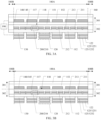
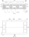
- FIG. 2 is a schematic planar view of a tactile reproduction display panel provided by an embodiment of the present disclosure.
- FIG. 3A is a schematic cross-sectional view of a tactile reproduction display panel taken along the line AB in FIG. 2 provided by an embodiment of the present disclosure.
- the tactile reproduction display panel 100 includes a display panel 110 and a plurality of piezoelectric vibration devices 120; the display panel 110 includes a base substrate 112 and a plurality of pixel units 200 located on the base substrate 112; each piezoelectric vibration device 120 includes a driver electrode structure 125 and a piezoelectric layer 122, and the driver electrode structure 125 is configured to drive the piezoelectric layer 122 to deform to generate vibration; the display panel 110 includes a light exiting surface 118, the light exiting surface 118 has a first side 301 and a second side 302 in the direction perpendicular to the base substrate 112, the light exiting surface 118 is configured to emit light to the first side 301, and the plurality of piezoelectric vibration devices 120 are located at the second side 302 of the light exiting surface 118.
- light exiting surface is the surface from which the light generated or transmitted by the display panel finally exits; the above-mentioned term “first side” may be the side of the light exiting surface away from the base substrate, and the above-mentioned term “second side” may be the side of the light exiting surface close to the base substrate.
- the tactile reproduction display panel because the plurality of piezoelectric vibration devices are located at the second side of the light exiting surface, the tactile reproduction display panel can also avoid the adverse influence cause by the plurality of piezoelectric vibration devices on light exiting, thereby reducing the frame width and achieving the narrow frame design; in addition, because the plurality of piezoelectric vibration devices are located at the second side of the light exiting surface, they can be better integrated with the display panel, thereby reducing the thickness of the touch-control reproduction display panel. On the other hand, because the tactile reproduction display panel does not need to be provided with a cavity or an air layer, it can avoid the defects such as reduction of luminous efficiency and noise caused by the cavity or the air layer.
- the above-mentioned base substrate is relative to the light exiting surface, and is used to define the position of the piezoelectric vibration devices, which is not necessarily the initial substrate in the manufacturing process of the display panel, but also the last formed substrate or layer.
- the surface of the initial substrate away from the light-emitting devices may be the light exiting surface, and the final formed cover plate or encapsulation layer may be the above-mentioned base substrate.
- the driver electrode structure 125 includes a first driving electrode 1251 and a second driving electrode 1252 that are respectively located on two sides of the piezoelectric layer 122 in the direction perpendicular to the base substrate 112.
- the second driving electrode 1251 and the second driving electrode 1252 can drive the piezoelectric layer 122 to vibrate.
- the plurality of piezoelectric vibration devices 120 are located at a side of the base substrate 112 away from the plurality of pixel units 200. That is, the plurality of piezoelectric vibration devices 120 are arranged on the back of the display panel 110. Therefore, the tactile reproduction display panel can prevent the plurality of piezoelectric vibration devices from adversely affecting the light-emitting display of the display panel.
- the display panel 110 includes a display area 110A and a peripheral area 110B surrounding the display area 110A, and the orthographic projection of at least part of the piezoelectric vibration device 120 on the display panel 110 overlaps with the display area 110A.
- the orthographic projection of the piezoelectric vibration device on the display panel overlaps with the display area, so that the piezoelectric vibration device can directly and better vibrate the display area of the tactile reproduction display panel; even if the piezoelectric vibration devices are arranged on the back of the display panel, a good vibration effect can still be obtained to achieve the simulation of different tactile sensations or tactile feelings.
- the tactile reproduction display panel can also be provided with piezoelectric vibration devices in the display area of the display panel, so that more piezoelectric vibration devices can be provided while avoiding the influence of piezoelectric vibration devices on the light-emitting display of the display panel, thereby improving the vibration effect and better achieving the simulation of different tactile sensations or tactile feelings.
- the above-mentioned term “display area” refers to the area on the display panel where pixel units are arranged and perform the light-emitting display
- the above-mentioned term “peripheral area” refers to the area on the display panel where no pixel units are arranged
- the above-mentioned terms “display area” and “peripheral area” divide the display panel in the horizontal direction, which can be used to define the position of piezoelectric vibration devices; therefore, the range defined by the "display area” in the present disclosure includes not only the light exiting side of the display panel, but also the back side of the display panel.
- the orthographic projections of the plurality of piezoelectric vibration devices 120 on the display panel 110 are all located in the display area 110A. Because the user's touch operation usually occurs in the display area, by arranging a plurality of piezoelectric vibration devices in the display area of the display panel, the tactile reproduction display panel can provide different vibration effects at different positions, so as to better achieve the simulation of different tactile sensations or tactile feelings.
- the tactile reproduction display panel can provide different vibration effects in different areas through piezoelectric vibration devices arranged in an array, so that better achieve the simulation of different tactile sensations or tactile feelings; on the other hand, the piezoelectric vibration devices arranged in array can also be controlled more conveniently.
- a plurality of pixel units 200 are arranged in an array along a row direction and a column direction, and the first direction X is parallel to the row direction or the column direction.
- the embodiments of the present disclosure include, but are not limited to this case, the above-mentioned first direction may form an included angle with the row direction, and the included angle is less than 90 degrees.
- the above row direction may be the extension direction of the gate line or the extension direction of the data line.
- the tactile reproduction display panel 100 further includes a cured adhesive layer 130, and the cured adhesive layer 130 is arranged between the piezoelectric vibration devices 120 and the base substrate 112, so that the piezoelectric vibration devices 120 can be fixed at the side of the base substrate 112 away from the plurality of pixel units 200. Because the cured adhesive layer can be fixed by a curing process (such as photocuring), the piezoelectric vibration devices can be fixed on the base substrate by the cured adhesive layer after the fabrication of the piezoelectric vibration devices is completed, thereby reducing the difficulty of the fabrication process of the tactile reproduction display panel and improving the production efficiency.
- a curing process such as photocuring
- the above-mentioned cured adhesive layer may be a photocurable adhesive layer, so that it can be cured by light at room temperature, therefore, on the one hand, the difficulty of manufacturing process of the cured adhesive layer can be reduced, on the other hand, adverse effects of high temperature on other devices can be avoided.
- the material of the cured adhesive layer may include epoxy resin.
- embodiments of the present disclosure include but are not limited to this case.
- the tactile reproduction display panel 100 further includes a touch structure 140; the touch structure 140 is located at the first side of the light exiting surface 118, that is, the touch structure 140 is located at the light exiting side of the display panel 110.
- the touch structure 140 includes a plurality of touch electrodes 145, the plurality of touch electrodes 145 are configured to detect the position of the touch operation. Therefore, the tactile reproduction display panel can detect the position of the touch operation, and can also control the piezoelectric vibration devices arranged in the display area array according to the position of the touch operation, so that the simulation of different tactile sensations or tactile feelings can be better achieved.
- the above-mentioned touch structure can adopt mutual capacitance touch technology or self-capacitance touch technology, and the embodiments of the present disclosure impose no limitation to this here.
- the tactile reproduction display panel 100 further includes a controller 190, the controller 190 is respectively connected with the piezoelectric vibration device 120 and the touch structure 140 in communication, so that the controller 190 can detect the position of the touch operation according to the signal output by the touch structure 140, and control the piezoelectric vibration devices according to the position of the touch operation.
- the above-mentioned term "connected with...in communication” includes the connection through wires, and may also include the connection through wireless communication.
- the tactile reproduction display panel 100 may include a first optical adhesive layer 151, a second optical adhesive layer 152 and an anti-reflective layer 160; the first optical adhesive layer 151 is located between the display panel 110 and the touch structure 140; the second optical adhesive layer 152 is located at the side of the touch structure 140 away from the display panel 110, and the anti-reflective layer 160 is located at the side of the second optical adhesive layer 152 away from the touch structure 140.
- the touch structure can be integrated on the display panel, thereby reducing the thickness of the tactile reproduction display panel; in addition, the tactile reproduction display panel can also avoid the reflection produced by the touch structure through the anti-reflection layer, thus avoiding the visualization of the touch structure.
- the anti-reflective layer may be a polarizer.
- the embodiments of the present disclosure include but are not limited to this case, and the above anti-reflective layer may also be other layers or structures with an anti-reflective function.
- At least one pixel unit 200 includes an organic light-emitting element 210; the organic light-emitting element 210 includes a first electrode 211, a second electrode 212, and an organic light-emitting function layer 213 located between the first electrode 211 and the second electrode 212. Therefore, because the display panel may be an organic light-emitting diode (OLED) display panel, the liquid crystal layer or the above-mentioned cavity or air layer can be avoided, so that the display panel can be better vibrated by the piezoelectric vibration devices, so as to better achieve the simulation of different tactile sensations.
- OLED organic light-emitting diode
- the embodiments of the present disclosure include but are not limited to this case, and the display panel may also be other types of display panels, such as a liquid crystal display panel.
- the above-mentioned organic light-emitting function layer may include not only a light-emitting layer that directly emits light, but also an auxiliary function layer for assisting light emission, such as a hole injection layer, a hole transport layer, an electron transport layer, and an electron injection layer.
- the above-mentioned base substrate may be at least one selected from a group consisting of a glass substrate, a silicon substrate and a plastic substrate.
- FIG. 3B is a schematic cross-sectional view of another tactile reproduction display panel provided by an embodiment of the present disclosure taken along the line AB in FIG. 2 .
- the display panel 110 includes an encapsulation layer 117, and the touch structure 140 is directly located on the encapsulation layer 117. Therefore, the integration level of the tactile reproduction display panel can be further improved and the thickness of the tactile reproduction display panel can be reduced.
- the tactile reproduction display panel 100 may include a third optical adhesive layer 153 and an anti-reflective layer 160; the third optical adhesive layer 153 is located at the side of the touch structure 140 away from the display panel 110, and the anti-reflection layer 160 is located at the side of the third optical adhesive layer 153 away from the touch structure 140. Therefore, the tactile reproduction display panel can also avoid the reflection produced by the touch structure through the anti-reflection layer, thereby avoiding the visualization of the touch structure.
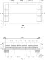
- FIG. 4 is a schematic planar view of a tactile reproduction display panel provided by an embodiment of the present disclosure.
- FIG. 5 is a schematic sectional view of the tactile reproduction display panel taken along the line CD in FIG. 4 provided by an embodiment of the present disclosure.
- the tactile reproduction display panel 100 includes a display panel 110 and a plurality of piezoelectric vibration devices 120; the display panel 110 includes a base substrate 112 and a plurality of pixel units 200 located on the base substrate 112; each piezoelectric vibration device 120 includes a driver electrode structure 125 and a piezoelectric layer 122, and the driver electrode structure 125 is configured to drive the piezoelectric layer 122 to deform to generate vibration; the display panel 110 includes a light exiting surface 118, the light exiting surface 118 has a first side 301 and a second side 302 in the direction perpendicular to the base substrate 112, and the light exiting surface 118 is configured to emit light to the first side 301.
- the plurality of piezoelectric vibration devices 120 are located at the side of the base substrate 112 away from the plurality of pixel units 200. That is, the plurality of piezoelectric vibration devices 120 are arranged on the back of the display panel 110.
- the display panel 110 includes a display area 110A and a peripheral area 110B surrounding the display area 110A, and orthographic projection of the plurality of piezoelectric vibration devices 120 on the display panel 110 overlap with the peripheral area 110a.
- the plurality of piezoelectric vibration devices 120 are also located at the second side 302 of the light exiting surface 118.
- the tactile reproduction display panel because the plurality of piezoelectric vibration devices are located at the side of the base substrate away from a plurality of pixel units, the tactile reproduction display panel can also avoid the adverse influence caused by the piezoelectric vibration devices on light output, thereby reducing the frame width and achieving the narrow frame design; in addition, because the plurality of piezoelectric vibration devices are located at the side of the base substrate away from the plurality of pixel units, the piezoelectric vibration devices can be better integrated with the display panel, thereby reducing the thickness of the touch reproduction display panel. On the other hand, because the tactile reproduction display panel does not need to be provided with a cavity or an air layer, the defects such as reduction of luminous efficiency and noise caused by the cavity or the air layer can be avoided.
- part of the orthographic projection of the plurality of piezoelectric vibration devices 120 on the display panel 110 is located in the display area 110A and part of the orthographic projection of the plurality of piezoelectric vibration devices 120 on the display panel 110 is located in the peripheral area 110B. Therefore, although the orthographic projection of the piezoelectric vibration devices on the base substrate overlaps with the display area, the size of the piezoelectric vibration device is not affected by the width of the peripheral area, and part of the piezoelectric vibration devices may be located in the display area.
- the plurality of piezoelectric vibration devices 120 may be arranged along the second direction to form two rows of piezoelectric vibration devices 120, one row of piezoelectric vibration devices 120 is arranged on an edge at the side of the display panel 110, and the other row of piezoelectric vibration devices 120 is arranged on an edge at the other side of the display panel.
- the tactile reproduction display panel 100 further includes a cured adhesive layer 130, and the cured adhesive layer 130 is arranged between the piezoelectric vibration devices 120 and the base substrate 112, so that the piezoelectric vibration devices 120 can be fixed at the side of the base substrate 112 away from the plurality of pixel units 200. Because the cured adhesive layer can be fixed by a curing process (such as photocuring), the piezoelectric vibration devices can be fixed on the base substrate by the cured adhesive layer after the fabrication of the piezoelectric vibration devices is completed, thereby reducing the difficulty of the fabrication process of the tactile reproduction display panel and improving the production efficiency.
- a curing process such as photocuring
- the above-mentioned cured adhesive layer may be a photocurable adhesive layer, so that it can be cured by light at room temperature, on the one hand, the difficulty of manufacturing process of the cured adhesive layer can be reduced, on the other hand, the adverse effects caused by high temperature on other devices can be avoided.
- the material of the cured adhesive layer may include epoxy resin.
- embodiments of the present disclosure include but are not limited to this case.
- the tactile reproduction display panel 100 further includes a touch structure 140 and an encapsulation layer 117, and the touch structure 140 is directly located on the encapsulation layer 117.
- the touch structure 140 is located at the first side of the light exiting surface 118, that is, the touch structure 140 is located at the light exiting side of the display panel 110.
- the touch structure 140 includes a plurality of touch electrodes 145, the plurality of touch electrodes 145 are configured to detect the position of the touch operation. Therefore, in the tactile reproduction display panel, the touch structure can be integrated on the display panel, and detection of the position of the touch operation can be achieved.
- the tactile reproduction display panel can also control piezoelectric vibration devices arranged in the display area array according to the position of touch operation, so that the simulation of different tactile sensations or tactile feelings can be better achieved.
- the embodiments of the present disclosure include but are not limited to this case, and the tactile reproduction display panel may also include a first optical adhesive layer, a second optical adhesive layer and an anti-reflective layer; the positional relationship and effect of the first optical adhesive layer, the second optical adhesive layer and the anti-reflective layer can be referred to the related descriptions of FIG. 3A , and are not described here again.
- the above-mentioned display panel may also be an organic light-emitting diode (OLED) display panel.
- OLED organic light-emitting diode
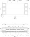
- FIG. 6 is a schematic planar view of a tactile reproduction display panel provided by an embodiment of the present disclosure.
- FIG. 7 is a schematic cross-sectional view of the tactile reproduction display panel taken along the line EF in FIG. 6 provided by an embodiment of the present disclosure.
- the tactile reproduction display panel 100 includes a display panel 110 and a plurality of piezoelectric vibration devices 120; the display panel 110 includes a base substrate 112 and a plurality of pixel units 200 located on the base substrate 112; each piezoelectric vibration device 120 includes a driver electrode structure 125 and a piezoelectric layer 122, and the driver electrode structure 125 is configured to drive the piezoelectric layer 122 to deform to generate vibration; the display panel 110 includes a light exiting surface 118, the light exiting surface 118 has a first side 301 and a second side 302 in the direction perpendicular to the base substrate 112, and the light exiting surface 118 is configured to emit light to the first side 301.
- the plurality of piezoelectric vibration devices 120 are located at the side of the base substrate 112 close to the light exiting surface 118; the plurality of piezoelectric vibration devices 120 are arranged side by side with at least part of the pixel units 120 on the base substrate 112; in this case, the plurality of piezoelectric vibration devices 120 are also located at the second side 302 of the light exiting surface 118.
- arranged side by side indicates that the plurality of piezoelectric vibration devices and at least part of the pixel units are arranged at the same side of the base substrate without overlapping each other; that is to say, the orthographic projection of the plurality of piezoelectric vibration devices on the base substrate does not overlap with the orthographic projection of at least part of the pixel units on the base substrate, or, the orthographic projection of the plurality of piezoelectric vibration devices on the base substrate are arranged at intervals with the orthographic projection of at least part of the pixel units on the base substrate.
- the touch reproduction display panel can be better integrated with the display panel, and the thickness of the touch reproduction display panel can be reduced.
- the tactile reproduction display panel does not need to be provided with a cavity or an air layer, the defects such as reduction of luminous efficiency and noise caused by the cavity or the air layer can be avoided.
- the display panel 110 includes a display area 110A and a peripheral area 110B surrounding the display area 110A, and the orthographic projection of the plurality of piezoelectric vibration devices 120 on the display panel 110 is located in the peripheral area 110B.
- the plurality of piezoelectric vibration devices are located at the side of the base substrate close to the light exiting surface, the integration between the piezoelectric vibration devices and the display panel is high, and the distance between the piezoelectric vibration devices and the display area is close, therefore, the frame width can also be reduced in the tactile reproduction display panel and the narrow frame design is achieved.
- the plurality of piezoelectric vibration devices 120 may be arranged along the second direction to form two rows of piezoelectric vibration devices 120, one row of piezoelectric vibration devices 120 is arranged at an edge at the side of the display panel 110, and the other row of piezoelectric vibration devices 120 is arranged at an edge at the other side of the display panel.
- the tactile reproduction display panel 100 further includes a touch structure 140 and an encapsulation layer 117, and the touch structure 140 is directly located on the encapsulation layer 117.
- the touch structure 140 is located on the first side of the light exiting surface 118, that is, the touch structure 140 is located on the light exiting side of the display panel 110.
- the touch structure 140 includes a plurality of touch electrodes 145, the plurality of touch electrodes 145 are configured to detect the position of the touch operation. Therefore, in the tactile reproduction display panel, the touch structure can be integrated on the display panel, and detection of the position of the touch operation can be achieved.
- the tactile reproduction display panel can also control the piezoelectric vibration devices arranged in an array in the display area according to the position of touch operation, so that the simulation of different tactile sensations or tactile feelings can be better achieved.
- the embodiment of the present disclosure includes but is not limited to this case, and the tactile reproduction display panel may also include a first optical adhesive layer, a second optical adhesive layer and an anti-reflective layer; the positional relationship and effect of the first optical adhesive layer, the second optical adhesive layer and the anti-reflective layer can be referred to the related description of FIG. 3A , and are not described here again.
- the above display panel may also be an organic light-emitting diode (OLED) display panel.
- OLED organic light-emitting diode
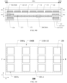
- FIG. 8 is a schematic planar view of a tactile reproduction display panel provided by an embodiment of the present disclosure.
- FIG. 9A is a schematic cross-sectional view of the tactile reproduction display panel taken along the line GH in FIG. 8 provided by an embodiment of the present disclosure.
- the tactile reproduction display panel 100 includes a display panel 110 and a plurality of piezoelectric vibration devices 120; the display panel 110 includes a base substrate 112 and a plurality of pixel units 200 located on the base substrate 112; each piezoelectric vibration device 120 includes a driver electrode structure 125 and a piezoelectric layer 122, and the driver electrode structure 125 is configured to drive the piezoelectric layer 122 to deform to generate vibration; the display panel 110 includes a light exiting surface 118, the light exiting surface 118 has a first side 301 and a second side 302 in the direction perpendicular to the base substrate 112, and the light exiting surface 118 is configured to emit light to the first side 301.
- the plurality of piezoelectric vibration devices 120 are located at the side of the base substrate 112 close to the light exiting surface 118.
- the plurality of piezoelectric vibration devices 120 are arranged side by side with at least part of the pixel units 120 on the base substrate 112;
- the display panel 110 includes a display area 110A and a peripheral area 110B surrounding the display area 110A, and the orthographic projection of at least part of the piezoelectric vibration device 120 on the display panel 110 is located in the display area 1 10a; in this case, the plurality of piezoelectric vibration devices 120 are also located at the second side 302 of the light exiting surface 118.
- the plurality of piezoelectric vibration devices are located at the side of the base substrate close to the light exiting surface, the plurality of piezoelectric vibration devices are also located at the second side of the light exiting surface, so that the display panel the tactile reproduction display panel can improve the integration between the piezoelectric vibration devices and the display panel, and meanwhile, prevent the piezoelectric vibration devices from adversely affecting the display of the display panel.
- the width of the peripheral area of the display panel can be regardless of the size of the piezoelectric vibration device, so can the frame width of the tactile reproduction display panel can be reduced and the narrow frame design is achieved.
- the thickness of the touch reproduction display panel of the tactile reproduction display panel can also be reduced.
- the tactile reproduction display panel does not need to be provided with a cavity or an air layer, the defects such as reduction of luminous efficiency and noise caused by the cavity or the air layer can be avoided.
- the plurality of pixel units 200 includes a plurality of first pixel units 200A and a plurality of second pixel units 200B, the plurality of first pixel units 200A and the plurality of second pixel units 200B are arranged side by side on the base substrate 112 with the plurality of piezoelectric vibration devices 200B, and the plurality of second pixel units 200B are located at the side of at least part of the piezoelectric vibration devices 120 away from the base substrate 112.
- the tactile reproduction display panel can improve the integration of the piezoelectric vibration device and the display panel, and meanwhile, prevent the piezoelectric vibration device from adversely affecting the display of the display panel.
- the above-mentioned terms "arranged side by side” indicates that the plurality of piezoelectric vibration devices and the plurality of first pixel units are arranged on the same side of the base substrate without overlapping each other; that is, the orthographic projection of the plurality of piezoelectric vibration devices on the base substrate do not overlap with the orthographic projection of the plurality of first pixel units on the base substrate, or, the orthographic projection of the plurality of piezoelectric vibration devices on the base substrate are arranged at intervals with the orthographic projection of the plurality of first pixel units on the base substrate.
- the orthographic projection of the plurality of second pixel units on the base substrate overlaps with the orthographic projection of at least part of the piezoelectric vibration device on the base substrate.
- the display area 100A includes a first display area 101A and a second display area 102A, the plurality of first pixel units 200A are located in the first display area 101A, the plurality of second pixel units 200B are located in the second display area 102A, and the second display area 102A is at the periphery of the first display area 101A.
- the second display area 102A is located on two sides of the first display area 101A in the first direction X.
- the tactile reproduction display panel 100 further includes a first insulation layer 171, the first insulation layer 171 is located at the side of the plurality of first pixel units 200A and the plurality of piezoelectric vibration devices 120 that are arranged side by side away from the base substrate 112; then, the plurality of second pixel units 200B are located at the side of the first insulation layer 171 away from the plurality of piezoelectric vibration devices 120.
- the tactile reproduction display panel can improve the integration of the piezoelectric vibration devices and the display panel, and meanwhile, prevent the piezoelectric vibration devices from adversely affecting the display of the display panel.
- the plurality of piezoelectric vibration devices 120 can be arranged along the second direction to form two columns of piezoelectric vibration devices 120, one column of piezoelectric vibration devices 120 is arranged at an edge at one side of the display panel 110, and the other column of piezoelectric vibration devices 120 is arranged at an edge at the other side of the display panel.
- the tactile reproduction display panel 100 further includes a touch structure 140 and an encapsulation layer 117, and the touch structure 140 is directly located on the encapsulation layer 117.
- the touch structure 140 is located on the first side of the light exiting surface 118, that is, the touch structure 140 is located on the light exiting side of the display panel 110.
- the touch structure 140 includes a plurality of touch electrodes 145, the plurality of touch electrodes 145 are configured to detect the position of the touch operation. Therefore, the touch structure can be integrated on the display panel in the tactile reproduction display panel, and detection of the position of the touch operation can be achieved.
- the tactile reproduction display panel can also control piezoelectric vibration devices arranged in the display area array according to the position of touch operation, so that the simulation of different tactile sensations or tactile feelings can be better achieved.
- the embodiment of the present disclosure includes but is not limited to this case, and the tactile reproduction display panel may also include a first optical adhesive layer, a second optical adhesive layer and an anti-reflective layer; the positional relationship and effect of the first optical adhesive layer, the second optical adhesive layer, and the anti-reflective layer can be referred to the related description of FIG. 3A , and are not described here again.
- the above display panel may also be an organic light-emitting diode (OLED) display panel.
- OLED organic light-emitting diode
- FIG. 9B is a schematic cross-sectional view of another tactile reproduction display panel taken along the line GH in FIG. 8 provided by an embodiment of the present disclosure.
- the tactile reproduction display panel 100 further includes a touch structure 172, the second insulation layer 172 is located at the side of the plurality of piezoelectric vibration devices 120 away from the base substrate 112; then, the plurality of pixel units 200 are located at the side of the insulation layer 171 away from the plurality of piezoelectric vibration devices 120. Therefore, the tactile reproduction display panel can improve the integration of the piezoelectric vibration device and the display panel, and meanwhile, avoid the adverse influence caused by the piezoelectric vibration device on the display of the display panel.
- the plurality of piezoelectric vibration devices 120 are located between the base substrate 112 and the second insulation layer 172, and the plurality of pixel units 200 are located at the side of the second insulation layer 172 away from the base substrate 112.
- the tactile reproduction display panel 100 further includes a touch structure 140 and an encapsulation layer 117, and the touch structure 140 is directly located on the encapsulation layer 117.
- the touch structure 140 is located on the first side of the light exiting surface 118, that is, the touch structure 140 is located on the light exiting side of the display panel 110.
- the touch structure 140 includes a plurality of touch electrodes 145, the plurality of touch electrodes 145 are configured to detect the position of the touch operation. Therefore, the touch structure can be integrated on the display panel in the tactile reproduction display panel, and detection of the position of the touch operation can be achieved.
- the tactile reproduction display panel can also control piezoelectric vibration devices arranged in the display area array according to the position of touch operation, so that simulation of different tactile sensations or tactile feelings can be better achieved.
- the embodiment of the present disclosure includes but is not limited to this case, and the tactile reproduction display panel may also include a first optical adhesive layer, a second optical adhesive layer and an anti-reflective layer; the positional relationship and effect of the first optical adhesive layer, the second optical adhesive layer, and the anti-reflective layer can be referred to the related description of FIG. 3A , and are not described here again.
- the above display panel may also be an organic light-emitting diode (OLED) display panel.
- OLED organic light-emitting diode
- FIG. 10 is a schematic planar view of a tactile reproduction display panel provided by an embodiment of the present disclosure.
- FIG. 11 is a schematic cross-sectional view of the tactile reproduction display panel taken along the line JK in FIG. 10 provided by an embodiment of the present disclosure.
- the tactile reproduction display panel 100 includes a display panel 110 and a plurality of piezoelectric vibration devices 120; the display panel 110 includes a base substrate 112 and a plurality of pixel units 200 located on the base substrate 112; each piezoelectric vibration device 120 includes a driver electrode structure 125 and a piezoelectric layer 122, and the driver electrode structure 125 is configured to drive the piezoelectric layer 122 to deform to generate vibration; the display panel 110 includes a light exiting surface 118, the light exiting surface 118 has a first side 301 and a second side 302 in the direction perpendicular to the base substrate 112, and the light exiting surface 118 is configured to emit light to the first side 301.
- the plurality of piezoelectric vibration devices 120 are located at the side of the base substrate 112 close to the light exiting surface 118.
- the plurality of piezoelectric vibration devices 120 are arranged side by side with at least part of the pixel units 120 on the base substrate 112;
- the display panel 110 includes a display area 110A and a peripheral area 110B surrounding the display area 110A, and the orthographic projection of at least part of the piezoelectric vibration devices 120 on the display panel 110 is located in the display area 110a;
- the plurality of pixel units 200 include a plurality of first pixel units 200A and a plurality of second pixel units 200B, the first pixel units 200A and the piezoelectric vibration devices 200B are arranged side by side on the base substrate 112, and the second pixel units 200B are located at the side of at least part of the piezoelectric vibration devices 120 away from the base substrate 112;
- the display area 100A includes a first display area 101A and a second display area 102A.
- the plurality of first pixel units 200A are located in the first display area 101A, and the plurality of second pixel units 200B are located in the second display area 101B, and the second display area 101B is surrounded by the first display area 101A.
- the plurality of piezoelectric vibration devices 120 are also located at the second side 302 of the light exiting surface 118.
- the tactile reproduction display panel provided by the embodiment of the present disclosure, by arranging the second pixel unit at the side of the piezoelectric vibration device away from the base substrate, the tactile reproduction display panel can improve the integration between the piezoelectric vibration devices and the display panel, and meanwhile, prevent the piezoelectric vibration devices from adversely affecting the display of the display panel.
- the width of the peripheral area of the display panel can be regardless of the size of the piezoelectric vibration device, therefore, the frame width of the tactile reproduction display panel can be reduced and the narrow frame design is achieved.
- the thickness of the touch reproduction display panel can also be reduced.
- the second display area is surrounded by the first display area, instead of being arranged on two sides or on edges of the first display area, so that piezoelectric vibration devices can be arranged in an array in the display area, thus providing better vibration effect and achieving simulation of different tactile sensations better.
- the tactile reproduction display panel 100 further includes a first insulation layer 171, the first insulation layer 171 is located at the side of the base substrate 112 close to the light exiting surface 118; the plurality of piezoelectric vibration devices 120 are located between the base substrate 112 and the first insulation layer 171, the first pixel unit 200A is located between the base substrate 112 and the first insulation layer 171, and the second pixel unit 200B is located at the side of the first insulation layer 171 away from the base substrate 112.
- the tactile display panel can improve the integration of the piezoelectric vibration devices and the display panel, and meanwhile, prevent the piezoelectric vibration device from adversely affecting the display of the display panel.
- the tactile reproduction display panel can provide different vibration effects in different areas through piezoelectric vibration devices arranged in an array, so that the simulation of different tactile sensations or tactile feelings can be better achieved; on the other hand, the piezoelectric vibration devices arranged in array can also be controlled more conveniently.
- the plurality of pixel units 200 are arranged in an array along a row direction and a column direction, and the first direction X is parallel to the row direction or the column direction.
- the embodiments of the present disclosure include, but are not limited to this case, the above-mentioned first direction may also form an included angle with the row direction, and the included angle is less than 90 degrees.
- the above row direction may be the extension direction of the gate line or the extension direction of the data line.
- the above-mentioned tactile reproduction display panel 100 further includes a touch structure 140 and an encapsulation layer 117, and the touch structure 140 is directly located on the encapsulation layer 117.
- the touch structure 140 is located on the first side of the light exiting surface 118, that is, the touch structure 140 is located on the light exiting side of the display panel 110.
- the touch structure 140 includes a plurality of touch electrodes 145, the plurality of touch electrodes 145 are configured to detect the position of the touch operation. Therefore, the touch structure can be integrated on the display panel in the tactile reproduction display panel, and the tactile reproduction display panel can detect the position of the touch operation.
- the tactile reproduction display panel can also control piezoelectric vibration devices arranged in the display area array according to the position of touch operation, so that the simulation of different tactile sensations or tactile feelings can be better achieved.
- the embodiment of the present disclosure includes but is not limited to this case, and the tactile reproduction display panel may also include a first optical adhesive layer, a second optical adhesive layer and an anti-reflective layer; the positional relationship and effect of the first optical adhesive layer, the second optical adhesive layer and the anti-reflective layer can be referred to the related description of FIG. 3A , and are not described here again.
- the tactile reproduction display panel may further include a controller, and the structure and positional relationship of the controller may be referred to the related descriptions of FIG. 2 and FIG. 3A , which are not described here again.
- FIG. 12 is a schematic planar view of a tactile reproduction display panel provided by an embodiment of the present disclosure.
- FIG. 13 is a schematic cross-sectional view of the tactile reproduction display panel taken along the line PQ in FIG. 12 provided by an embodiment of the present disclosure.
- the tactile reproduction display panel 100 includes a display panel 110, a touch structure 140 and a plurality of piezoelectric vibration devices 120.
- the display panel 110 includes a base substrate 112 and a plurality of pixel units 200 located on the base substrate 112; the touch structure 140 includes a plurality of touch electrodes 145, the plurality of touch electrodes 145 are configured to detect the position of the touch operation; each piezoelectric vibration device 120 includes a driver electrode structure 125 and a piezoelectric layer 122, and the driver electrode structure 125 is configured to drive the piezoelectric layer 122 to deform to generate vibration; the plurality of piezoelectric vibration devices 120 are located at the side of the touch structure 140 away from the display panel 110.
- the display panel 110 includes a display area 100A and a peripheral area 100B surrounding the display area 100A, and the orthographic projection of the piezoelectric vibration devices 120 on the display panel 110 is located in the peripheral area 100.
- the tactile reproduction display panel provided by the embodiment of the present disclosure, because the plurality of piezoelectric vibration devices are located at the side of the touch structure away from the display panel, the piezoelectric vibration devices do not need to be provided with a cavity or an air layer, so that the defects such as reduction of luminous efficiency and noise caused by the cavity or the air layer can be avoided.
- the tactile reproduction display panel integrates the display panel, the touch structure and the piezoelectric vibration devices together, so that the thickness of the entire tactile reproduction display panel can be reduced.
- the tactile reproduction display panel 100 further includes a touch structure 140 directly located on the display panel 110. Therefore, the thickness of the tactile reproduction display panel can be further reduced.
- the tactile reproduction display panel 100 may include a third optical adhesive layer 153 and an anti-reflective layer 160; the third optical adhesive layer 153 is located at the side of the touch structure 140 away from the display panel 110, and the anti-reflection layer 160 is located at the side of the third optical adhesive layer 153 away from the touch structure 140. Therefore, the tactile reproduction display panel can also avoid the reflection produced by the touch structure through the anti-reflection layer, thereby avoiding the visualization of the touch structure.
- the piezoelectric vibration device 120 may be directly arranged on the surface of the anti-reflective layer 160 away from the base substrate 112.
- the embodiment of the present disclosure includes but is not limited to this case, and the tactile reproduction display panel may also include a first optical adhesive layer, a second optical adhesive layer and an anti-reflective layer; the positional relationship and effect of the first optical adhesive layer, the second optical adhesive layer and the anti-reflective layer can be referred to the related description of Fig.3A , and are described here again.
- At least one pixel unit 200 includes a liquid crystal display unit 220, the liquid crystal display unit 220 includes a pixel electrode 221, a common electrode 222, and a liquid crystal layer 223 located between the pixel electrode 221 and the common electrode 222. Therefore, the display panel may be a liquid crystal display panel.
- the embodiments of the present disclosure include but are not limited to this case, and the above display panel may also be replaced by an organic light-emitting diode (OLED) display panel.
- OLED organic light-emitting diode
- the display panel may also be an organic light-emitting diode (OLED) display panel.
- OLED organic light-emitting diode
- FIG. 14 is a schematic planar view of a tactile reproduction display panel provided by an embodiment of the present disclosure.
- FIG. 15 is a schematic cross-sectional view of the tactile reproduction display panel taken along the line MN in FIG. 14 provided by an embodiment of the present disclosure.
- the tactile reproduction display panel 100 further includes a display panel 110, a plurality of piezoelectric vibration devices 120 and a common substrate 180; each piezoelectric vibration device 120 includes a driver electrode structure 125 and a piezoelectric layer 122, and the driver electrode structure 125 is configured to drive the piezoelectric layer 122 to deform to generate vibration; the display panel 110 and the plurality of piezoelectric vibration devices 120 are located on the common substrate 180.
- the piezoelectric vibration devices do not need to be provided with a cavity or an air layer, so that the defects such as reduction of luminous efficiency and noise caused by the cavity or the air layer can be avoided.
- the display panel and the plurality of piezoelectric vibration devices are located on the common substrate, the thickness of the tactile reproduction display panel can be reduced; in addition, the tactile reproduction display panel can better deform the display panel through piezoelectric vibration devices to generate vibration, and improve the vibration effect.
- the above-mentioned tactile reproduction display panel 100 further includes a touch structure 140 and an encapsulation layer 117, and the touch structure 140 is directly located on the encapsulation layer 117. Therefore, the thickness of the tactile reproduction display panel can be further reduced.
- the embodiment of the present disclosure includes but is not limited to this case, and the tactile reproduction display panel may also include a first optical adhesive layer, a second optical adhesive layer and an anti-reflective layer; the positional relationship and effect of the first optical adhesive layer, the second optical adhesive layer and the anti-reflective layer can be referred to the related description of FIG. 3A , and are not described here again.
- the above-mentioned display panel may also be an organic light-emitting diode (OLED) display panel.
- OLED organic light-emitting diode
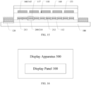
- FIG. 16 is a schematic diagram of a display apparatus provided by an embodiment of the present disclosure.
- the display apparatus 500 includes the tactile reproduction display panel 100 described above. Therefore, the display apparatus also has the beneficial technical effects corresponding to the technical effects of the included tactile reproduction display panel. These beneficial technical effects can be referred to the related descriptions of the tactile reproduction display panel, which are not repeated here.
- the display apparatus can be an electronic product with display function, such as a mobile phone, a tablet computer, a display, a TV set, a navigator and the like.
Landscapes
- Engineering & Computer Science (AREA)
- Physics & Mathematics (AREA)
- General Engineering & Computer Science (AREA)
- Theoretical Computer Science (AREA)
- General Physics & Mathematics (AREA)
- Human Computer Interaction (AREA)
- Nonlinear Science (AREA)
- Crystallography & Structural Chemistry (AREA)
- Optics & Photonics (AREA)
- Chemical & Material Sciences (AREA)
- Mathematical Physics (AREA)
- Position Input By Displaying (AREA)
- Devices For Indicating Variable Information By Combining Individual Elements (AREA)
Abstract
Description
- Embodiments of the present disclosure relate to a tactile reproduction display panel and a display apparatus.
- At present, Haptics is the focus of current technology development, the concept of Haptics is that with the help of haptic technology, electronic equipment manufacturers can create distinctive personalized haptic feedback for specific interactive experiences on their devices, thus providing consumers with more valuable and realistic unique experiences.
- Haptics can be divided into two categories, one is vibration feedback and the other is tactile reproduction technology. Vibration feedback is to provide tactile feedback and vibration reminder for users by adding a linear motor to a redisplay device. Surface tactile reproduction technology can perceive the characteristics of objects by touching the screen with the skin (fingertips), and can achieve efficient and realistic interaction in multimedia terminals, which has great research value, so it has been widely concerned by researchers at home and abroad. In physical sense, the surface tactile sensation means interaction on the surface of the object and the surface of the skin (fingertip), and different friction forces are formed due to different surface structures. Therefore, different tactile sensations or tactile feelings can be simulated by controlling the surface friction.
- Embodiments of the present disclosure provide a tactile reproduction display panel and a display apparatus including the tactile reproduction display panel. The tactile reproduction display panel includes a display panel and a plurality of piezoelectric vibration devices; the display panel includes a base substrate and a plurality of pixel units on the base substrate; each of the piezoelectric vibration devices includes a driver electrode structure and a piezoelectric layer, and the driver electrode structure is configured to drive the piezoelectric layer to deform so as to generate vibration; the display panel includes a light exiting surface, the light exiting surface has a first side and a second side in a direction perpendicular to the base substrate, the light exiting surface is configured to emit light to the first side, and the plurality of piezoelectric vibration devices are at the second side of the light exiting surface. In the tactile reproduction display panel provided by the embodiment of the present disclosure, because the plurality of piezoelectric vibration devices are located at the second side of the light exiting surface, the tactile reproduction display panel can avoid adverse effects of the plurality of piezoelectric vibration devices on exiting light, thereby reducing the frame width and achieving a narrow frame design; in addition, because the plurality of piezoelectric vibration devices are located at the second side of the light exiting surface, they can be better integrated with the display panel, thereby reducing the thickness of the touch-control reproduction display panel. On the other hand, because the tactile reproduction display panel does not need to be provided with a cavity or an air layer, it can avoid the defects such as reduction of luminous efficiency and noise caused by the cavity or the air layer.
- At least one embodiment of the present disclosure provides a tactile reproduction display panel, which includes: a display panel including a base substrate and a plurality of pixel units on the base substrate; and a plurality of piezoelectric vibration devices, each of the piezoelectric vibration devices includes a driver electrode structure and a piezoelectric layer, and the driver electrode structure is configured to drive the piezoelectric layer to deform so as to generate vibration; the display panel includes a light exiting surface, the light exiting surface has a first side and a second side in a direction perpendicular to the base substrate, the light exiting surface is configured to emit light to the first side, and the plurality of piezoelectric vibration devices are at the second side of the light exiting surface.
- For example, in the tactile reproduction display panel provided by an embodiment of the present disclosure, the plurality of piezoelectric vibration devices are at a side of the base substrate away from the plurality of pixel units.
- For example, in the tactile reproduction display panel provided by an embodiment of the present disclosure, the display panel includes a display area and a peripheral area surrounding the display area, and an orthographic projection of at least part of the plurality of piezoelectric vibration devices on the display panel is in the display area.
- For example, in the tactile reproduction display panel provided by an embodiment of the present disclosure, orthographic projections of the plurality of piezoelectric vibration devices on the display panel are all in the display area.
- For example, in the tactile reproduction display panel provided by an embodiment of the present disclosure, in the display area, at least part of the piezoelectric vibration devices is arranged in an array along a first direction and a second direction, and the first direction intersects with the second direction.
- For example, in the tactile reproduction display panel provided by an embodiment of the present disclosure, the plurality of pixel units are arranged in an array along a row direction and a column direction, and the first direction is parallel to the row direction or the column direction.
- For example, in the tactile reproduction display panel provided by an embodiment of the present disclosure, the display panel includes a display area and a peripheral area surrounding the display area, and an orthographic projection of the plurality of piezoelectric vibration devices on the display panel is in the peripheral area.
- For example, the tactile reproduction display panel provided by an embodiment of the present disclosure further includes: a cured adhesive layer, between the plurality of piezoelectric vibration devices and the base substrate.
- For example, in the tactile reproduction display panel provided by an embodiment of the present disclosure, the plurality of piezoelectric vibration devices are at a side of the base substrate close to the light exiting surface.
- For example, in the tactile reproduction display panel provided by an embodiment of the present disclosure, the plurality of piezoelectric vibration devices are arranged side by side with at least part of the plurality of pixel units on the base substrate.
- For example, in the tactile reproduction display panel provided by an embodiment of the present disclosure, the display panel includes a display area and a peripheral area surrounding the display area, and an orthographic projection of the plurality of piezoelectric vibration devices on the display panel is in the peripheral area.
- For example, in the tactile reproduction display panel provided by an embodiment of the present disclosure, the display panel includes a display area and a peripheral area surrounding the display area, and an orthographic projection of at least part of the plurality of piezoelectric vibration devices on the display panel overlaps with the display area.
- For example, in the tactile reproduction display panel provided by an embodiment of the present disclosure, the plurality of pixel units include a plurality of first pixel units and a plurality of second pixel units, the first pixel units and the plurality of piezoelectric vibration devices are arranged side by side on the base substrate, and the second pixel units are at a side of at least part of the plurality of piezoelectric vibration devices away from the base substrate.
- For example, in the tactile reproduction display panel provided by an embodiment of the present disclosure, the display area includes a first display area and a second display area, the plurality of first pixel units are in the first display area, the plurality of second pixel units are in the second display area, and the second display area is at a periphery of the first display area.
- For example, in the tactile reproduction display panel provided by an embodiment of the present disclosure, the display area includes a first display area and a second display area, the plurality of first pixel units are in the first display area, the plurality of second pixel units are in the second display area, and the second display area is surrounded by the first display area.
- For example, the tactile reproduction display panel provided by an embodiment of the present disclosure further includes: a first insulation layer, at a side of the plurality of first pixel units and the plurality of piezoelectric vibration devices that are arranged side by side away from the base substrate, the plurality of second pixel units are at a side of the first insulation layer away from the plurality of piezoelectric vibration devices.
- For example, the tactile reproduction display panel provided by an embodiment of the present disclosure further includes: a second insulation layer, at a side of the base substrate close to the light exiting surface, the plurality of piezoelectric vibration devices are between the base substrate and the second insulation layer, and the plurality of pixel units are at a side of the second insulation layer away from the base substrate.
- For example, the tactile reproduction display panel provided by an embodiment of the present disclosure, further includes: a touch structure, at the first side of the light exiting surface, the touch structure includes a plurality of touch electrodes, and the plurality of touch electrodes are configured to detect a position of s touch operation.
- For example, the tactile reproduction display panel provided by an embodiment of the present disclosure further includes: a first optical adhesive layer, between the display panel and the touch structure; a second optical adhesive layer, at a side of the touch structure away from the display panel; and an anti-reflective layer, at a side of the second optical adhesive layer away from the touch structure.
- For example, in the tactile reproduction display panel provided by an embodiment of the present disclosure, the display panel includes an encapsulation layer, and the touch structure is directly on the encapsulation layer.
- For example, in the tactile reproduction display panel provided by an embodiment of the present disclosure, at least one of the pixel units includes an organic light-emitting element, the organic light-emitting element includes a first electrode, a second electrode, and an organic light-emitting function layer between the first electrode and the second electrode.
- For example, in the tactile reproduction display panel provided by an embodiment of the present disclosure, at least one of the pixel units includes a liquid crystal display unit, the liquid crystal display unit includes a pixel electrode, a common electrode, and a liquid crystal layer between the pixel electrode and the common electrode.
- For example, in the tactile reproduction display panel provided by an embodiment of the present disclosure, the base substrate includes at least one selected from a group consisting of a glass base substrate, a silicon base substrate and a plastic base substrate.
- At least one embodiment of the present disclosure further provides a tactile reproduction display panel, which includes: a display panel, including a base substrate and a plurality of pixel units on the base substrate; a touch structure, including a plurality of touch electrodes configured to detect a position of a touch operation; and a plurality of piezoelectric vibration devices, each of the plurality of piezoelectric vibration devices includes a driver electrode structure and a piezoelectric layer, and the driver electrode structure is configured to drive the piezoelectric layer to deform so as to generate vibration; the plurality of piezoelectric vibration devices are at a side of the touch structure away from the display panel, the display panel includes a display area and a peripheral area surrounding the display area, and an orthographic projection of the plurality of piezoelectric vibration devices on the display panel is in the peripheral area.
- At least one embodiment of the present disclosure further provides a tactile reproduction display panel, which includes: a display panel, including a base substrate and a plurality of pixel units on the base substrate; a plurality of piezoelectric vibration devices; and a common base substrate, each of the plurality of piezoelectric vibration devices includes a driver electrode structure and a piezoelectric layer, and the driver electrode structure is configured to drive the piezoelectric layer to deform so as to generate vibration; the display panel and the plurality of piezoelectric vibration devices are on the common base substrate.
- At least one embodiment of the present disclosure provides a display apparatus, which includes any one of the tactile reproduction display panels as described above.
- In order to clearly illustrate the technical solution of the embodiments of the present disclosure, the drawings of the embodiments will be briefly described. It is obvious that the described drawings in the following are only related to some embodiments of the present disclosure and thus are not construed as any limitation to the present disclosure.
-
FIG. 1 is a schematic structural diagram of a tactile reproduction display panel. -
FIG. 2 is a schematic planar view of a tactile reproduction display panel provided by an embodiment of the present disclosure. -
FIG. 3A is a schematic cross-sectional view of the tactile reproduction display panel taken along the line AB inFIG. 2 provided by an embodiment of the present disclosure. -
FIG. 3B is a schematic cross-sectional view of another tactile reproduction display panel provided by an embodiment of the present disclosure taken along the line AB inFIG. 2 . -
FIG. 4 is a schematic planar view of a tactile reproduction display panel provided by an embodiment of the present disclosure. -
FIG. 5 is a schematic sectional view of the tactile reproduction display panel taken along the CD line inFIG. 4 provided by an embodiment of the present disclosure. -
FIG. 6 is a schematic planar view of a tactile reproduction display panel provided by an embodiment of the present disclosure. -
FIG. 7 is a schematic cross-sectional view of the tactile reproduction display panel taken along the EF line inFIG. 6 provided by an embodiment of the present disclosure. -
FIG. 8 is a schematic planar view of a tactile reproduction display panel provided by an embodiment of the present disclosure. -
FIG. 9A is a schematic cross-sectional view of the tactile reproduction display panel taken along the GH line inFIG. 8 provided by an embodiment of the present disclosure. -
FIG. 9B is a schematic cross-sectional view of another tactile reproduction display panel taken along the GH line inFIG. 8 provided by an embodiment of the present disclosure. -
FIG. 10 is a schematic planar view of a tactile reproduction display panel provided by an embodiment of the present disclosure. -
FIG. 11 is a schematic cross-sectional view of the tactile reproduction display panel taken along the line JK inFIG. 10 provided by an embodiment of the present disclosure. -
FIG. 12 is a schematic planar view of a tactile reproduction display panel provided by an embodiment of the present disclosure. -
FIG. 13 is a schematic cross-sectional view of the tactile reproduction display panel taken along the line PQ inFIG. 12 provided by an embodiment of the present disclosure. -
FIG. 14 is a schematic planar view of a tactile reproduction display panel provided by an embodiment of the present disclosure. -
FIG. 15 is a schematic cross-sectional view of the tactile reproduction display panel taken along the line MN inFIG. 14 provided by an embodiment of the present disclosure. -
FIG. 16 is a schematic diagram of a display apparatus provided by an embodiment of the present disclosure. - In order to make objectives, technical details, and advantages of the embodiments of the present disclosure more clear, the technical solutions of the embodiments will be described in a clearly and fully understandable way in connection with the drawings related to the embodiments of the present disclosure. Apparently, the described embodiments are just a part but not all of the embodiments of the present disclosure. Based on the described embodiments herein, those skilled in the art can obtain other embodiment(s), without any inventive work, which should be within the scope of the present disclosure.
- Unless otherwise defined, all the technical and scientific terms used herein have the same meanings as commonly understood by one of ordinary skill in the art to which the present disclosure belongs. The terms "first", "second", etc., which are used in the present disclosure, are not intended to indicate any sequence, amount or importance, but distinguish various components. Also, the terms "comprise," "comprising," "include," "including," etc., are intended to specify that the elements or the objects stated before these terms encompass the elements or the objects and equivalents thereof listed after these terms, but do not preclude the other elements or objects. The phrases "connect", "connected", etc., are not intended to define a physical connection or mechanical connection, but may include an electrical connection, directly or indirectly. "On," "under," "left," "right" and the like are only used to indicate relative position relationship, and when the position of the object which is described is changed, the relative position relationship may be changed accordingly.
- Unless otherwise defined, features such as "parallel", "perpendicular" and "same" used in the embodiments of the present disclosure all include situations such as "parallel", "perpendicular", and "same" in the strict sense, and also include situations such as "approximately parallel", "approximately perpendicular", "approximately the same" that contain certain errors. For example, the above "approximately" may mean that difference of compared objects is within 10% of an average value of the compared objects, or within 5% of an average value of the compared objects. In a case that a number of components or elements is not specifically indicated below in the embodiments of the present disclosure, it refers to that the components or elements may be one or more, or may be understood as at least one. "At least one" means one or more, and "a plurality" means at least two. The "arranged on a same layer" in the embodiments of the present disclosure refers to a relationship between a plurality of film layers formed by a same material after going through a same step (for example, an one-step patterning process). The "same layer" here does not always refer to that the plurality of film layers have the same thickness or that the plurality of film layers have the same height in cross-sectional schematic diagrams.
- In the technical field of surface tactile reproduction, vibration devices can be used as vibration sources to make the screen vibrate, so that the surface of the screen forms different friction forces, so that different tactile sensations or tactile sensations can be simulated. On the other hand, the piezoelectric vibration device is very suitable as a vibration device integrated on the screen because of its small size and good vibration effect.
-
FIG. 1 is a schematic structural diagram of a tactile reproduction display panel. As illustrated byFIG. 1 , the tactilereproduction display panel 10 includes a liquidcrystal display panel 11, atouch panel 12 and apiezoelectric vibration device 13; the liquidcrystal display panel 11 includes adisplay area 11A and aperipheral area 11B surrounding thedisplay area 11A; thetouch panel 12 is located on the light exiting side of the liquidcrystal display panel 11; thepiezoelectric vibration device 13 is located at the side of thetouch panel 12 away from the liquidcrystal display panel 11. Because thepiezoelectric vibration device 13 is opaque to light, thepiezoelectric vibration device 13 can only be disposed in theperipheral area 11B of the liquidcrystal display panel 11. In this case, in order to enable thetouch panel 12 to have a better vibration effect, it is required to set acavity 14 between thedisplay panel 11 and thetouch panel 12; for example, the thickness of thecavity 14 may be greater than 500 microns. However, on the one hand, because thepiezoelectric vibration device 13 is arranged in the peripheral area of the liquidcrystal display panel 11 and is opaque to light, it is easy to cause the width of the non-display area at the edge of the tactilereproduction display panel 10 to be large, making it difficult to achieve the narrow frame design, and the thickness of the tactilereproduction display panel 10 is also large due to the existence of thecavity 14 and thepiezoelectric vibration device 13; on the other hand, because thecavity 14 is arranged between thedisplay panel 11 and thetouch panel 12, it is easy to cause total reflection of the light emitted from thedisplay panel 11 at the interface between thecavity 14 and thedisplay panel 11 or the interface between thecavity 14 and thetouch panel 12, which reduces the light extraction efficiency. In addition, the sound generated by thepiezoelectric vibration device 13 resonates in thecavity 14 for many times easily, which results in noise. - In one aspect, embodiments of the present disclosure provide a tactile reproduction display panel and a display apparatus including the tactile reproduction display panel. The tactile reproduction display panel includes a display panel and a plurality of piezoelectric vibration devices; the display panel includes a base substrate and a plurality of pixel units on the base substrate; each of the piezoelectric vibration devices includes a driver electrode structure and a piezoelectric layer, and the driver electrode structure is configured to drive the piezoelectric layer to deform so as to generate vibration; the display panel includes a light exiting surface, the light exiting surface has a first side and a second side in a direction perpendicular to the base substrate, the light exiting surface is configured to emit light to the first side, and the plurality of piezoelectric vibration devices are at the second side of the light exiting surface. In the tactile reproduction display panel provided by the embodiment of the present disclosure, because the plurality of piezoelectric vibration devices are located at the second side of the light exiting surface, the tactile reproduction display panel can avoid adverse effects of the plurality of piezoelectric vibration devices on exiting light, thereby reducing the frame width and achieving a narrow frame design; in addition, because the plurality of piezoelectric vibration devices are located at the second side of the light exiting surface, they can be better integrated with the display panel, thereby reducing the thickness of the touch-control reproduction display panel. On the other hand, because the tactile reproduction display panel does not need to be provided with a cavity or an air layer, it can avoid the defects such as reduction of luminous efficiency and noise caused by the cavity or the air layer.
- On the other hand, the embodiment of the present disclosure further provides another tactile reproduction display panel and a display apparatus including the tactile reproduction display panel. The tactile reproduction display panel includes a display panel, a touch structure, and a plurality of piezoelectric vibration devices; the display panel includes a base substrate and a plurality of pixel units on the base substrate; the touch structure includes a plurality of touch electrodes configured to detect a position of a touch operation; each of the plurality of piezoelectric vibration devices includes a driver electrode structure and a piezoelectric layer, and the driver electrode structure is configured to drive the piezoelectric layer to deform so as to generate vibration; the plurality of piezoelectric vibration devices are at a side of the touch structure away from the display panel, the display panel includes a display area and a peripheral area surrounding the display area, and an orthographic projection of the plurality of piezoelectric vibration devices on the display panel is in the peripheral area. In the tactile reproduction display panel provided by the embodiment of the present disclosure, the plurality of piezoelectric vibration devices are located at the side of the touch structure away from the display panel, and the display panel includes a display area and a peripheral area surrounding the display area, so that the touch structure and the plurality of piezoelectric vibration devices are integrated on the display panel in the tactile reproduction display panel, thereby improving the vibration effect and reducing the thickness of the tactile reproduction display panel. On the other hand, because the tactile reproduction display panel does not need to be provided with a cavity or an air layer, it can avoid the defects such as reduction of luminous efficiency and noise caused by the cavity or the air layer.
- On the other hand, the embodiment of the present disclosure further provides still another tactile reproduction display panel and a display apparatus including the tactile reproduction display panel. The tactile reproduction display panel includes a display panel, a plurality of piezoelectric vibration devices, and a common substrate; the display panel includes a base substrate and a plurality of pixel units on the base substrate; each of the plurality of piezoelectric vibration devices includes a driver electrode structure and a piezoelectric layer, and the driver electrode structure is configured to drive the piezoelectric layer to deform so as to generate vibration; the display panel and the plurality of piezoelectric vibration devices are on the common base substrate. In the tactile reproduction display panel provided by the embodiment of the present disclosure, because the display panel and the plurality of piezoelectric vibration devices are located on the common substrate, the tactile reproduction display panel can improve the vibration effect and also reduce the thickness of the tactile reproduction display panel. On the other hand, because the tactile reproduction display panel does not need to be provided with a cavity or an air layer, it can avoid the defects such as reduction of luminous efficiency and noise caused by the cavity or the air layer.
- Hereinafter, the tactile reproduction display panel and display apparatus provided by the embodiments of the present disclosure will be described in detail with reference to the accompanying drawings.
-
FIG. 2 is a schematic planar view of a tactile reproduction display panel provided by an embodiment of the present disclosure.FIG. 3A is a schematic cross-sectional view of a tactile reproduction display panel taken along the line AB inFIG. 2 provided by an embodiment of the present disclosure. - As illustrated by
FIG. 2 andFIG. 3A , the tactilereproduction display panel 100 includes adisplay panel 110 and a plurality ofpiezoelectric vibration devices 120; thedisplay panel 110 includes abase substrate 112 and a plurality ofpixel units 200 located on thebase substrate 112; eachpiezoelectric vibration device 120 includes a driver electrode structure 125 and apiezoelectric layer 122, and the driver electrode structure 125 is configured to drive thepiezoelectric layer 122 to deform to generate vibration; thedisplay panel 110 includes alight exiting surface 118, thelight exiting surface 118 has afirst side 301 and asecond side 302 in the direction perpendicular to thebase substrate 112, thelight exiting surface 118 is configured to emit light to thefirst side 301, and the plurality ofpiezoelectric vibration devices 120 are located at thesecond side 302 of thelight exiting surface 118. It should be noted that the above-mentioned term "light exiting surface" is the surface from which the light generated or transmitted by the display panel finally exits; the above-mentioned term "first side" may be the side of the light exiting surface away from the base substrate, and the above-mentioned term "second side" may be the side of the light exiting surface close to the base substrate. - In the tactile reproduction display panel provided by the embodiment of the present disclosure, because the plurality of piezoelectric vibration devices are located at the second side of the light exiting surface, the tactile reproduction display panel can also avoid the adverse influence cause by the plurality of piezoelectric vibration devices on light exiting, thereby reducing the frame width and achieving the narrow frame design; in addition, because the plurality of piezoelectric vibration devices are located at the second side of the light exiting surface, they can be better integrated with the display panel, thereby reducing the thickness of the touch-control reproduction display panel. On the other hand, because the tactile reproduction display panel does not need to be provided with a cavity or an air layer, it can avoid the defects such as reduction of luminous efficiency and noise caused by the cavity or the air layer.
- It is worth noting that the above-mentioned base substrate is relative to the light exiting surface, and is used to define the position of the piezoelectric vibration devices, which is not necessarily the initial substrate in the manufacturing process of the display panel, but also the last formed substrate or layer. For example, in the case that the display panel is an organic light-emitting diode display panel with bottom emission type, the surface of the initial substrate away from the light-emitting devices may be the light exiting surface, and the final formed cover plate or encapsulation layer may be the above-mentioned base substrate.
- In some examples, as illustrated by
FIG. 2 andFIG. 3A , the driver electrode structure 125 includes a first driving electrode 1251 and a second driving electrode 1252 that are respectively located on two sides of thepiezoelectric layer 122 in the direction perpendicular to thebase substrate 112. Thus, the second driving electrode 1251 and the second driving electrode 1252 can drive thepiezoelectric layer 122 to vibrate. - In some examples, as illustrated by
FIG. 2 andFIG. 3A , the plurality ofpiezoelectric vibration devices 120 are located at a side of thebase substrate 112 away from the plurality ofpixel units 200. That is, the plurality ofpiezoelectric vibration devices 120 are arranged on the back of thedisplay panel 110. Therefore, the tactile reproduction display panel can prevent the plurality of piezoelectric vibration devices from adversely affecting the light-emitting display of the display panel. - In some examples, as illustrated by
FIG. 2 andFIG. 3A , thedisplay panel 110 includes a display area 110A and a peripheral area 110B surrounding the display area 110A, and the orthographic projection of at least part of thepiezoelectric vibration device 120 on thedisplay panel 110 overlaps with the display area 110A. In this way, the orthographic projection of the piezoelectric vibration device on the display panel overlaps with the display area, so that the piezoelectric vibration device can directly and better vibrate the display area of the tactile reproduction display panel; even if the piezoelectric vibration devices are arranged on the back of the display panel, a good vibration effect can still be obtained to achieve the simulation of different tactile sensations or tactile feelings. In addition, because the orthographic projection of piezoelectric vibration devices on the display panel overlaps with the display area, the tactile reproduction display panel can also be provided with piezoelectric vibration devices in the display area of the display panel, so that more piezoelectric vibration devices can be provided while avoiding the influence of piezoelectric vibration devices on the light-emitting display of the display panel, thereby improving the vibration effect and better achieving the simulation of different tactile sensations or tactile feelings. - It should be noted that the above-mentioned term "display area" refers to the area on the display panel where pixel units are arranged and perform the light-emitting display, and the above-mentioned term "peripheral area" refers to the area on the display panel where no pixel units are arranged; in addition, the above-mentioned terms "display area" and "peripheral area" divide the display panel in the horizontal direction, which can be used to define the position of piezoelectric vibration devices; therefore, the range defined by the "display area" in the present disclosure includes not only the light exiting side of the display panel, but also the back side of the display panel.
- In some examples, as illustrated by
FIG. 2 andFIG. 3A , the orthographic projections of the plurality ofpiezoelectric vibration devices 120 on thedisplay panel 110 are all located in the display area 110A. Because the user's touch operation usually occurs in the display area, by arranging a plurality of piezoelectric vibration devices in the display area of the display panel, the tactile reproduction display panel can provide different vibration effects at different positions, so as to better achieve the simulation of different tactile sensations or tactile feelings. - In some examples, as illustrated by
FIG. 2 andFIG. 3A , in the display area 110A, at least part of thepiezoelectric vibration devices 120 are arranged in an array along a first direction X and a second direction Y, and the first direction X intersects with the second direction Y. Therefore, on the one hand, the tactile reproduction display panel can provide different vibration effects in different areas through piezoelectric vibration devices arranged in an array, so that better achieve the simulation of different tactile sensations or tactile feelings; on the other hand, the piezoelectric vibration devices arranged in array can also be controlled more conveniently. - In some examples, as illustrated by
FIG. 2 andFIG. 3A , a plurality ofpixel units 200 are arranged in an array along a row direction and a column direction, and the first direction X is parallel to the row direction or the column direction. Of course, the embodiments of the present disclosure include, but are not limited to this case, the above-mentioned first direction may form an included angle with the row direction, and the included angle is less than 90 degrees. It should be noted that the above row direction may be the extension direction of the gate line or the extension direction of the data line. - In some examples, as illustrated by
FIG. 2 andFIG. 3A , the tactilereproduction display panel 100 further includes a curedadhesive layer 130, and the curedadhesive layer 130 is arranged between thepiezoelectric vibration devices 120 and thebase substrate 112, so that thepiezoelectric vibration devices 120 can be fixed at the side of thebase substrate 112 away from the plurality ofpixel units 200. Because the cured adhesive layer can be fixed by a curing process (such as photocuring), the piezoelectric vibration devices can be fixed on the base substrate by the cured adhesive layer after the fabrication of the piezoelectric vibration devices is completed, thereby reducing the difficulty of the fabrication process of the tactile reproduction display panel and improving the production efficiency. - In some examples, the above-mentioned cured adhesive layer may be a photocurable adhesive layer, so that it can be cured by light at room temperature, therefore, on the one hand, the difficulty of manufacturing process of the cured adhesive layer can be reduced, on the other hand, adverse effects of high temperature on other devices can be avoided.
- In some examples, the material of the cured adhesive layer may include epoxy resin. Of course, embodiments of the present disclosure include but are not limited to this case.
- In some examples, as illustrated by
FIG. 2 andFIG. 3A , the tactilereproduction display panel 100 further includes a touch structure 140; the touch structure 140 is located at the first side of thelight exiting surface 118, that is, the touch structure 140 is located at the light exiting side of thedisplay panel 110. The touch structure 140 includes a plurality of touch electrodes 145, the plurality of touch electrodes 145 are configured to detect the position of the touch operation. Therefore, the tactile reproduction display panel can detect the position of the touch operation, and can also control the piezoelectric vibration devices arranged in the display area array according to the position of the touch operation, so that the simulation of different tactile sensations or tactile feelings can be better achieved. It should be noted that the above-mentioned touch structure can adopt mutual capacitance touch technology or self-capacitance touch technology, and the embodiments of the present disclosure impose no limitation to this here. - In some examples, as illustrated by
FIG. 2 andFIG. 3A , the tactilereproduction display panel 100 further includes acontroller 190, thecontroller 190 is respectively connected with thepiezoelectric vibration device 120 and the touch structure 140 in communication, so that thecontroller 190 can detect the position of the touch operation according to the signal output by the touch structure 140, and control the piezoelectric vibration devices according to the position of the touch operation. It should be noted that the above-mentioned term "connected with...in communication" includes the connection through wires, and may also include the connection through wireless communication. - In some examples, as illustrated by
FIG. 2 andFIG. 3A , the tactilereproduction display panel 100 may include a first opticaladhesive layer 151, a second opticaladhesive layer 152 and ananti-reflective layer 160; the first opticaladhesive layer 151 is located between thedisplay panel 110 and the touch structure 140; the second opticaladhesive layer 152 is located at the side of the touch structure 140 away from thedisplay panel 110, and theanti-reflective layer 160 is located at the side of the second opticaladhesive layer 152 away from the touch structure 140. Therefore, in the tactile reproduction display panel, the touch structure can be integrated on the display panel, thereby reducing the thickness of the tactile reproduction display panel; in addition, the tactile reproduction display panel can also avoid the reflection produced by the touch structure through the anti-reflection layer, thus avoiding the visualization of the touch structure. - In some examples, the anti-reflective layer may be a polarizer. Of course, the embodiments of the present disclosure include but are not limited to this case, and the above anti-reflective layer may also be other layers or structures with an anti-reflective function.
- In some examples, as illustrated by
FIG. 2 andFIG. 3A , at least onepixel unit 200 includes an organic light-emitting element 210; the organic light-emitting element 210 includes afirst electrode 211, asecond electrode 212, and an organic light-emittingfunction layer 213 located between thefirst electrode 211 and thesecond electrode 212. Therefore, because the display panel may be an organic light-emitting diode (OLED) display panel, the liquid crystal layer or the above-mentioned cavity or air layer can be avoided, so that the display panel can be better vibrated by the piezoelectric vibration devices, so as to better achieve the simulation of different tactile sensations. Of course, the embodiments of the present disclosure include but are not limited to this case, and the display panel may also be other types of display panels, such as a liquid crystal display panel. It should be noted that the above-mentioned organic light-emitting function layer may include not only a light-emitting layer that directly emits light, but also an auxiliary function layer for assisting light emission, such as a hole injection layer, a hole transport layer, an electron transport layer, and an electron injection layer. - In some examples, the above-mentioned base substrate may be at least one selected from a group consisting of a glass substrate, a silicon substrate and a plastic substrate.
-
FIG. 3B is a schematic cross-sectional view of another tactile reproduction display panel provided by an embodiment of the present disclosure taken along the line AB inFIG. 2 . - In some examples, as illustrated by
FIGS. 2 and3B , thedisplay panel 110 includes anencapsulation layer 117, and the touch structure 140 is directly located on theencapsulation layer 117. Therefore, the integration level of the tactile reproduction display panel can be further improved and the thickness of the tactile reproduction display panel can be reduced. - In some examples, as illustrated by
FIGS. 2 and3B , the tactilereproduction display panel 100 may include a third opticaladhesive layer 153 and ananti-reflective layer 160; the third opticaladhesive layer 153 is located at the side of the touch structure 140 away from thedisplay panel 110, and theanti-reflection layer 160 is located at the side of the third opticaladhesive layer 153 away from the touch structure 140. Therefore, the tactile reproduction display panel can also avoid the reflection produced by the touch structure through the anti-reflection layer, thereby avoiding the visualization of the touch structure. -
FIG. 4 is a schematic planar view of a tactile reproduction display panel provided by an embodiment of the present disclosure.FIG. 5 is a schematic sectional view of the tactile reproduction display panel taken along the line CD inFIG. 4 provided by an embodiment of the present disclosure. - As illustrated by
FIG. 4 and FIG. 5 , the tactilereproduction display panel 100 includes adisplay panel 110 and a plurality ofpiezoelectric vibration devices 120; thedisplay panel 110 includes abase substrate 112 and a plurality ofpixel units 200 located on thebase substrate 112; eachpiezoelectric vibration device 120 includes a driver electrode structure 125 and apiezoelectric layer 122, and the driver electrode structure 125 is configured to drive thepiezoelectric layer 122 to deform to generate vibration; thedisplay panel 110 includes alight exiting surface 118, thelight exiting surface 118 has afirst side 301 and asecond side 302 in the direction perpendicular to thebase substrate 112, and thelight exiting surface 118 is configured to emit light to thefirst side 301. - As illustrated by
FIG. 4 and FIG. 5 , the plurality ofpiezoelectric vibration devices 120 are located at the side of thebase substrate 112 away from the plurality ofpixel units 200. That is, the plurality ofpiezoelectric vibration devices 120 are arranged on the back of thedisplay panel 110. Thedisplay panel 110 includes a display area 110A and a peripheral area 110B surrounding the display area 110A, and orthographic projection of the plurality ofpiezoelectric vibration devices 120 on thedisplay panel 110 overlap with the peripheral area 110a. In this case, the plurality ofpiezoelectric vibration devices 120 are also located at thesecond side 302 of thelight exiting surface 118. - In the tactile reproduction display panel provided by the embodiment of the present disclosure, because the plurality of piezoelectric vibration devices are located at the side of the base substrate away from a plurality of pixel units, the tactile reproduction display panel can also avoid the adverse influence caused by the piezoelectric vibration devices on light output, thereby reducing the frame width and achieving the narrow frame design; in addition, because the plurality of piezoelectric vibration devices are located at the side of the base substrate away from the plurality of pixel units, the piezoelectric vibration devices can be better integrated with the display panel, thereby reducing the thickness of the touch reproduction display panel. On the other hand, because the tactile reproduction display panel does not need to be provided with a cavity or an air layer, the defects such as reduction of luminous efficiency and noise caused by the cavity or the air layer can be avoided.
- In some examples, as illustrated by
FIG. 4 and FIG. 5 , part of the orthographic projection of the plurality ofpiezoelectric vibration devices 120 on thedisplay panel 110 is located in the display area 110A and part of the orthographic projection of the plurality ofpiezoelectric vibration devices 120 on thedisplay panel 110 is located in the peripheral area 110B. Therefore, although the orthographic projection of the piezoelectric vibration devices on the base substrate overlaps with the display area, the size of the piezoelectric vibration device is not affected by the width of the peripheral area, and part of the piezoelectric vibration devices may be located in the display area. - In some examples, as illustrated by
FIG. 4 and FIG. 5 , the plurality ofpiezoelectric vibration devices 120 may be arranged along the second direction to form two rows ofpiezoelectric vibration devices 120, one row ofpiezoelectric vibration devices 120 is arranged on an edge at the side of thedisplay panel 110, and the other row ofpiezoelectric vibration devices 120 is arranged on an edge at the other side of the display panel. - In some examples, as illustrated by
FIG. 4 and FIG. 5 , the tactilereproduction display panel 100 further includes a curedadhesive layer 130, and the curedadhesive layer 130 is arranged between thepiezoelectric vibration devices 120 and thebase substrate 112, so that thepiezoelectric vibration devices 120 can be fixed at the side of thebase substrate 112 away from the plurality ofpixel units 200. Because the cured adhesive layer can be fixed by a curing process (such as photocuring), the piezoelectric vibration devices can be fixed on the base substrate by the cured adhesive layer after the fabrication of the piezoelectric vibration devices is completed, thereby reducing the difficulty of the fabrication process of the tactile reproduction display panel and improving the production efficiency. - In some examples, the above-mentioned cured adhesive layer may be a photocurable adhesive layer, so that it can be cured by light at room temperature, on the one hand, the difficulty of manufacturing process of the cured adhesive layer can be reduced, on the other hand, the adverse effects caused by high temperature on other devices can be avoided.
- In some examples, the material of the cured adhesive layer may include epoxy resin. Of course, embodiments of the present disclosure include but are not limited to this case.
- In some examples, as illustrated by
FIG. 4 and FIG. 5 , the tactilereproduction display panel 100 further includes a touch structure 140 and anencapsulation layer 117, and the touch structure 140 is directly located on theencapsulation layer 117. The touch structure 140 is located at the first side of thelight exiting surface 118, that is, the touch structure 140 is located at the light exiting side of thedisplay panel 110. The touch structure 140 includes a plurality of touch electrodes 145, the plurality of touch electrodes 145 are configured to detect the position of the touch operation. Therefore, in the tactile reproduction display panel, the touch structure can be integrated on the display panel, and detection of the position of the touch operation can be achieved. On the other hand, the tactile reproduction display panel can also control piezoelectric vibration devices arranged in the display area array according to the position of touch operation, so that the simulation of different tactile sensations or tactile feelings can be better achieved. - Of course, the embodiments of the present disclosure include but are not limited to this case, and the tactile reproduction display panel may also include a first optical adhesive layer, a second optical adhesive layer and an anti-reflective layer; the positional relationship and effect of the first optical adhesive layer, the second optical adhesive layer and the anti-reflective layer can be referred to the related descriptions of
FIG. 3A , and are not described here again. - In some examples, as illustrated by
FIG. 4 and FIG. 5 , the above-mentioned display panel may also be an organic light-emitting diode (OLED) display panel. The specific structure and effect of the above-mentioned organic light-emitting diode (OLED) display panel can be seen in the relevant descriptions ofFIG. 2 andFIG. 3A , and are not described here again. -
FIG. 6 is a schematic planar view of a tactile reproduction display panel provided by an embodiment of the present disclosure.FIG. 7 is a schematic cross-sectional view of the tactile reproduction display panel taken along the line EF inFIG. 6 provided by an embodiment of the present disclosure. - As illustrated by
FIG. 6 and FIG. 7 , the tactilereproduction display panel 100 includes adisplay panel 110 and a plurality ofpiezoelectric vibration devices 120; thedisplay panel 110 includes abase substrate 112 and a plurality ofpixel units 200 located on thebase substrate 112; eachpiezoelectric vibration device 120 includes a driver electrode structure 125 and apiezoelectric layer 122, and the driver electrode structure 125 is configured to drive thepiezoelectric layer 122 to deform to generate vibration; thedisplay panel 110 includes alight exiting surface 118, thelight exiting surface 118 has afirst side 301 and asecond side 302 in the direction perpendicular to thebase substrate 112, and thelight exiting surface 118 is configured to emit light to thefirst side 301. - As illustrated by
FIG. 6 and FIG. 7 , the plurality ofpiezoelectric vibration devices 120 are located at the side of thebase substrate 112 close to thelight exiting surface 118; the plurality ofpiezoelectric vibration devices 120 are arranged side by side with at least part of thepixel units 120 on thebase substrate 112; in this case, the plurality ofpiezoelectric vibration devices 120 are also located at thesecond side 302 of thelight exiting surface 118. It should be noted that the above-mentioned term " arranged side by side" indicates that the plurality of piezoelectric vibration devices and at least part of the pixel units are arranged at the same side of the base substrate without overlapping each other; that is to say, the orthographic projection of the plurality of piezoelectric vibration devices on the base substrate does not overlap with the orthographic projection of at least part of the pixel units on the base substrate, or, the orthographic projection of the plurality of piezoelectric vibration devices on the base substrate are arranged at intervals with the orthographic projection of at least part of the pixel units on the base substrate. - In the tactile reproduction display panel provided by the embodiment of the present disclosure, because the plurality of piezoelectric vibration devices are located at the side of the base substrate close to the light exiting surface, that is, the piezoelectric vibration devices are arranged inside the display panel, the touch reproduction display panel can be better integrated with the display panel, and the thickness of the touch reproduction display panel can be reduced. On the other hand, because the tactile reproduction display panel does not need to be provided with a cavity or an air layer, the defects such as reduction of luminous efficiency and noise caused by the cavity or the air layer can be avoided.
- In some examples, as illustrated by
FIG. 6 and FIG. 7 , thedisplay panel 110 includes a display area 110A and a peripheral area 110B surrounding the display area 110A, and the orthographic projection of the plurality ofpiezoelectric vibration devices 120 on thedisplay panel 110 is located in the peripheral area 110B. Although the plurality of piezoelectric vibration devices are located at the side of the base substrate close to the light exiting surface, the integration between the piezoelectric vibration devices and the display panel is high, and the distance between the piezoelectric vibration devices and the display area is close, therefore, the frame width can also be reduced in the tactile reproduction display panel and the narrow frame design is achieved. - In some examples, as illustrated by
FIG. 6 and FIG. 7 , the plurality ofpiezoelectric vibration devices 120 may be arranged along the second direction to form two rows ofpiezoelectric vibration devices 120, one row ofpiezoelectric vibration devices 120 is arranged at an edge at the side of thedisplay panel 110, and the other row ofpiezoelectric vibration devices 120 is arranged at an edge at the other side of the display panel. - In some examples, as illustrated by
FIG. 6 and FIG. 7 , the tactilereproduction display panel 100 further includes a touch structure 140 and anencapsulation layer 117, and the touch structure 140 is directly located on theencapsulation layer 117. The touch structure 140 is located on the first side of thelight exiting surface 118, that is, the touch structure 140 is located on the light exiting side of thedisplay panel 110. The touch structure 140 includes a plurality of touch electrodes 145, the plurality of touch electrodes 145 are configured to detect the position of the touch operation. Therefore, in the tactile reproduction display panel, the touch structure can be integrated on the display panel, and detection of the position of the touch operation can be achieved. On the other hand, the tactile reproduction display panel can also control the piezoelectric vibration devices arranged in an array in the display area according to the position of touch operation, so that the simulation of different tactile sensations or tactile feelings can be better achieved. - Of course, the embodiment of the present disclosure includes but is not limited to this case, and the tactile reproduction display panel may also include a first optical adhesive layer, a second optical adhesive layer and an anti-reflective layer; the positional relationship and effect of the first optical adhesive layer, the second optical adhesive layer and the anti-reflective layer can be referred to the related description of
FIG. 3A , and are not described here again. - In some examples, as illustrated by
FIG. 4 and FIG. 5 , the above display panel may also be an organic light-emitting diode (OLED) display panel. The specific structure and effect of the above-mentioned organic light-emitting diode (OLED) display panel can be seen in the related descriptions ofFIG. 2 andFIG. 3A , and are not described here again. -
FIG. 8 is a schematic planar view of a tactile reproduction display panel provided by an embodiment of the present disclosure.FIG. 9A is a schematic cross-sectional view of the tactile reproduction display panel taken along the line GH inFIG. 8 provided by an embodiment of the present disclosure. - As illustrated by
FIG. 8 and FIG. 9A , the tactilereproduction display panel 100 includes adisplay panel 110 and a plurality ofpiezoelectric vibration devices 120; thedisplay panel 110 includes abase substrate 112 and a plurality ofpixel units 200 located on thebase substrate 112; eachpiezoelectric vibration device 120 includes a driver electrode structure 125 and apiezoelectric layer 122, and the driver electrode structure 125 is configured to drive thepiezoelectric layer 122 to deform to generate vibration; thedisplay panel 110 includes alight exiting surface 118, thelight exiting surface 118 has afirst side 301 and asecond side 302 in the direction perpendicular to thebase substrate 112, and thelight exiting surface 118 is configured to emit light to thefirst side 301. - As illustrated by
FIG. 8 and FIG. 9A , the plurality ofpiezoelectric vibration devices 120 are located at the side of thebase substrate 112 close to thelight exiting surface 118. The plurality ofpiezoelectric vibration devices 120 are arranged side by side with at least part of thepixel units 120 on thebase substrate 112; thedisplay panel 110 includes a display area 110A and a peripheral area 110B surrounding the display area 110A, and the orthographic projection of at least part of thepiezoelectric vibration device 120 on thedisplay panel 110 is located in the display area 1 10a; in this case, the plurality ofpiezoelectric vibration devices 120 are also located at thesecond side 302 of thelight exiting surface 118. - In the tactile reproduction display panel provided by the embodiment of the present disclosure, although the plurality of piezoelectric vibration devices are located at the side of the base substrate close to the light exiting surface, the plurality of piezoelectric vibration devices are also located at the second side of the light exiting surface, so that the display panel the tactile reproduction display panel can improve the integration between the piezoelectric vibration devices and the display panel, and meanwhile, prevent the piezoelectric vibration devices from adversely affecting the display of the display panel. In this case, the width of the peripheral area of the display panel can be regardless of the size of the piezoelectric vibration device, so can the frame width of the tactile reproduction display panel can be reduced and the narrow frame design is achieved. In addition, because the display panel and the piezoelectric vibration device can be better integrated together, the thickness of the touch reproduction display panel of the tactile reproduction display panel can also be reduced. On the other hand, because the tactile reproduction display panel does not need to be provided with a cavity or an air layer, the defects such as reduction of luminous efficiency and noise caused by the cavity or the air layer can be avoided.
- In some examples, as illustrated by
FIG. 8 and FIG. 9A , the plurality ofpixel units 200 includes a plurality offirst pixel units 200A and a plurality ofsecond pixel units 200B, the plurality offirst pixel units 200A and the plurality ofsecond pixel units 200B are arranged side by side on thebase substrate 112 with the plurality ofpiezoelectric vibration devices 200B, and the plurality ofsecond pixel units 200B are located at the side of at least part of thepiezoelectric vibration devices 120 away from thebase substrate 112. By arranging the second pixel unit at the side of the piezoelectric vibration device away from the base substrate, the tactile reproduction display panel can improve the integration of the piezoelectric vibration device and the display panel, and meanwhile, prevent the piezoelectric vibration device from adversely affecting the display of the display panel. - It should be noted that the above-mentioned terms "arranged side by side" indicates that the plurality of piezoelectric vibration devices and the plurality of first pixel units are arranged on the same side of the base substrate without overlapping each other; that is, the orthographic projection of the plurality of piezoelectric vibration devices on the base substrate do not overlap with the orthographic projection of the plurality of first pixel units on the base substrate, or, the orthographic projection of the plurality of piezoelectric vibration devices on the base substrate are arranged at intervals with the orthographic projection of the plurality of first pixel units on the base substrate. However, because the plurality of second pixel units are located at the side of at least part of the piezoelectric vibration device away from the base substrate, the orthographic projection of the plurality of second pixel units on the base substrate overlaps with the orthographic projection of at least part of the piezoelectric vibration device on the base substrate.
- In some examples, as illustrated by
FIG. 8 and FIG. 9A , thedisplay area 100A includes afirst display area 101A and asecond display area 102A, the plurality offirst pixel units 200A are located in thefirst display area 101A, the plurality ofsecond pixel units 200B are located in thesecond display area 102A, and thesecond display area 102A is at the periphery of thefirst display area 101A. - In some examples, as illustrated by
FIG. 8 and FIG. 9A , thesecond display area 102A is located on two sides of thefirst display area 101A in the first direction X. - In some examples, as illustrated by
FIG. 8 and FIG. 9A , the tactilereproduction display panel 100 further includes afirst insulation layer 171, thefirst insulation layer 171 is located at the side of the plurality offirst pixel units 200A and the plurality ofpiezoelectric vibration devices 120 that are arranged side by side away from thebase substrate 112; then, the plurality ofsecond pixel units 200B are located at the side of thefirst insulation layer 171 away from the plurality ofpiezoelectric vibration devices 120. Therefore, by arranging the first insulation layer and arranging the second pixel unit at the side of the piezoelectric vibration device away from the base substrate, the tactile reproduction display panel can improve the integration of the piezoelectric vibration devices and the display panel, and meanwhile, prevent the piezoelectric vibration devices from adversely affecting the display of the display panel. - In some examples, as illustrated by
FIG. 8 and FIG. 9A , the plurality ofpiezoelectric vibration devices 120 can be arranged along the second direction to form two columns ofpiezoelectric vibration devices 120, one column ofpiezoelectric vibration devices 120 is arranged at an edge at one side of thedisplay panel 110, and the other column ofpiezoelectric vibration devices 120 is arranged at an edge at the other side of the display panel. - In some examples, as illustrated by
FIG. 8 and FIG. 9A , the tactilereproduction display panel 100 further includes a touch structure 140 and anencapsulation layer 117, and the touch structure 140 is directly located on theencapsulation layer 117. The touch structure 140 is located on the first side of thelight exiting surface 118, that is, the touch structure 140 is located on the light exiting side of thedisplay panel 110. The touch structure 140 includes a plurality of touch electrodes 145, the plurality of touch electrodes 145 are configured to detect the position of the touch operation. Therefore, the touch structure can be integrated on the display panel in the tactile reproduction display panel, and detection of the position of the touch operation can be achieved. On the other hand, the tactile reproduction display panel can also control piezoelectric vibration devices arranged in the display area array according to the position of touch operation, so that the simulation of different tactile sensations or tactile feelings can be better achieved. - Of course, the embodiment of the present disclosure includes but is not limited to this case, and the tactile reproduction display panel may also include a first optical adhesive layer, a second optical adhesive layer and an anti-reflective layer; the positional relationship and effect of the first optical adhesive layer, the second optical adhesive layer, and the anti-reflective layer can be referred to the related description of
FIG. 3A , and are not described here again. - In some examples, as illustrated by
FIG. 8 and FIG. 9A , the above display panel may also be an organic light-emitting diode (OLED) display panel. The specific structure and effect of the above-mentioned organic light-emitting diode (OLED) display panel can be seen in the related descriptions ofFIG. 2 andFIG. 3A , and are not described here again. -
FIG. 9B is a schematic cross-sectional view of another tactile reproduction display panel taken along the line GH inFIG. 8 provided by an embodiment of the present disclosure. - In some examples, as illustrated by
FIG. 8 andFIG. 9B , the tactilereproduction display panel 100 further includes atouch structure 172, thesecond insulation layer 172 is located at the side of the plurality ofpiezoelectric vibration devices 120 away from thebase substrate 112; then, the plurality ofpixel units 200 are located at the side of theinsulation layer 171 away from the plurality ofpiezoelectric vibration devices 120. Therefore, the tactile reproduction display panel can improve the integration of the piezoelectric vibration device and the display panel, and meanwhile, avoid the adverse influence caused by the piezoelectric vibration device on the display of the display panel. - In some examples, as illustrated by
FIG. 8 andFIG. 9B , the plurality ofpiezoelectric vibration devices 120 are located between thebase substrate 112 and thesecond insulation layer 172, and the plurality ofpixel units 200 are located at the side of thesecond insulation layer 172 away from thebase substrate 112. - In some examples, as illustrated by
FIG. 8 andFIG. 9B , the tactilereproduction display panel 100 further includes a touch structure 140 and anencapsulation layer 117, and the touch structure 140 is directly located on theencapsulation layer 117. The touch structure 140 is located on the first side of thelight exiting surface 118, that is, the touch structure 140 is located on the light exiting side of thedisplay panel 110. The touch structure 140 includes a plurality of touch electrodes 145, the plurality of touch electrodes 145 are configured to detect the position of the touch operation. Therefore, the touch structure can be integrated on the display panel in the tactile reproduction display panel, and detection of the position of the touch operation can be achieved. On the other hand, the tactile reproduction display panel can also control piezoelectric vibration devices arranged in the display area array according to the position of touch operation, so that simulation of different tactile sensations or tactile feelings can be better achieved. - Of course, the embodiment of the present disclosure includes but is not limited to this case, and the tactile reproduction display panel may also include a first optical adhesive layer, a second optical adhesive layer and an anti-reflective layer; the positional relationship and effect of the first optical adhesive layer, the second optical adhesive layer, and the anti-reflective layer can be referred to the related description of
FIG. 3A , and are not described here again. - In some examples, as illustrated by
FIG. 8 andFIG. 9B , the above display panel may also be an organic light-emitting diode (OLED) display panel. The specific structure and effect of the above-mentioned organic light-emitting diode (OLED) display panel can be seen in the related descriptions ofFIG. 2 andFIG. 3A , and are not described here again. -
FIG. 10 is a schematic planar view of a tactile reproduction display panel provided by an embodiment of the present disclosure.FIG. 11 is a schematic cross-sectional view of the tactile reproduction display panel taken along the line JK inFIG. 10 provided by an embodiment of the present disclosure. - As illustrated by
FIG. 10 andFIG. 11 , the tactilereproduction display panel 100 includes adisplay panel 110 and a plurality ofpiezoelectric vibration devices 120; thedisplay panel 110 includes abase substrate 112 and a plurality ofpixel units 200 located on thebase substrate 112; eachpiezoelectric vibration device 120 includes a driver electrode structure 125 and apiezoelectric layer 122, and the driver electrode structure 125 is configured to drive thepiezoelectric layer 122 to deform to generate vibration; thedisplay panel 110 includes alight exiting surface 118, thelight exiting surface 118 has afirst side 301 and asecond side 302 in the direction perpendicular to thebase substrate 112, and thelight exiting surface 118 is configured to emit light to thefirst side 301. - As illustrated by
FIG. 10 andFIG. 11 , the plurality ofpiezoelectric vibration devices 120 are located at the side of thebase substrate 112 close to thelight exiting surface 118. The plurality ofpiezoelectric vibration devices 120 are arranged side by side with at least part of thepixel units 120 on thebase substrate 112; thedisplay panel 110 includes a display area 110A and a peripheral area 110B surrounding the display area 110A, and the orthographic projection of at least part of thepiezoelectric vibration devices 120 on thedisplay panel 110 is located in the display area 110a; the plurality ofpixel units 200 include a plurality offirst pixel units 200A and a plurality ofsecond pixel units 200B, thefirst pixel units 200A and thepiezoelectric vibration devices 200B are arranged side by side on thebase substrate 112, and thesecond pixel units 200B are located at the side of at least part of thepiezoelectric vibration devices 120 away from thebase substrate 112; thedisplay area 100A includes afirst display area 101A and asecond display area 102A. The plurality offirst pixel units 200A are located in thefirst display area 101A, and the plurality ofsecond pixel units 200B are located in the second display area 101B, and the second display area 101B is surrounded by thefirst display area 101A. In this case, the plurality ofpiezoelectric vibration devices 120 are also located at thesecond side 302 of thelight exiting surface 118. - In the tactile reproduction display panel provided by the embodiment of the present disclosure, by arranging the second pixel unit at the side of the piezoelectric vibration device away from the base substrate, the tactile reproduction display panel can improve the integration between the piezoelectric vibration devices and the display panel, and meanwhile, prevent the piezoelectric vibration devices from adversely affecting the display of the display panel. In this case, the width of the peripheral area of the display panel can be regardless of the size of the piezoelectric vibration device, therefore, the frame width of the tactile reproduction display panel can be reduced and the narrow frame design is achieved. In addition, because the display panel and the piezoelectric vibration device can be better integrated together, the thickness of the touch reproduction display panel can also be reduced. On the other hand, the second display area is surrounded by the first display area, instead of being arranged on two sides or on edges of the first display area, so that piezoelectric vibration devices can be arranged in an array in the display area, thus providing better vibration effect and achieving simulation of different tactile sensations better.
- In some examples, as illustrated by
FIG. 10 andFIG. 11 , the tactilereproduction display panel 100 further includes afirst insulation layer 171, thefirst insulation layer 171 is located at the side of thebase substrate 112 close to thelight exiting surface 118; the plurality ofpiezoelectric vibration devices 120 are located between thebase substrate 112 and thefirst insulation layer 171, thefirst pixel unit 200A is located between thebase substrate 112 and thefirst insulation layer 171, and thesecond pixel unit 200B is located at the side of thefirst insulation layer 171 away from thebase substrate 112. Therefore, by arranging the second insulation layer and arranging the plurality of pixel units at the side of the second insulation layer away from the base substrate, the tactile display panel can improve the integration of the piezoelectric vibration devices and the display panel, and meanwhile, prevent the piezoelectric vibration device from adversely affecting the display of the display panel. - In some examples, as illustrated by
FIG. 10 andFIG. 11 , in the display area 110A, at least part of thepiezoelectric vibration devices 120 are arranged in an array along a first direction X and a second direction Y, and the first direction X intersects with the second direction Y. Therefore, on the one hand, the tactile reproduction display panel can provide different vibration effects in different areas through piezoelectric vibration devices arranged in an array, so that the simulation of different tactile sensations or tactile feelings can be better achieved; on the other hand, the piezoelectric vibration devices arranged in array can also be controlled more conveniently. - In some examples, as illustrated by
FIG. 10 andFIG. 11 , the plurality ofpixel units 200 are arranged in an array along a row direction and a column direction, and the first direction X is parallel to the row direction or the column direction. Of course, the embodiments of the present disclosure include, but are not limited to this case, the above-mentioned first direction may also form an included angle with the row direction, and the included angle is less than 90 degrees. It should be noted that the above row direction may be the extension direction of the gate line or the extension direction of the data line. - In some examples, as illustrated by
FIG. 10 andFIG. 11 , the above-mentioned tactilereproduction display panel 100 further includes a touch structure 140 and anencapsulation layer 117, and the touch structure 140 is directly located on theencapsulation layer 117. The touch structure 140 is located on the first side of thelight exiting surface 118, that is, the touch structure 140 is located on the light exiting side of thedisplay panel 110. The touch structure 140 includes a plurality of touch electrodes 145, the plurality of touch electrodes 145 are configured to detect the position of the touch operation. Therefore, the touch structure can be integrated on the display panel in the tactile reproduction display panel, and the tactile reproduction display panel can detect the position of the touch operation. On the other hand, the tactile reproduction display panel can also control piezoelectric vibration devices arranged in the display area array according to the position of touch operation, so that the simulation of different tactile sensations or tactile feelings can be better achieved. - Of course, the embodiment of the present disclosure includes but is not limited to this case, and the tactile reproduction display panel may also include a first optical adhesive layer, a second optical adhesive layer and an anti-reflective layer; the positional relationship and effect of the first optical adhesive layer, the second optical adhesive layer and the anti-reflective layer can be referred to the related description of
FIG. 3A , and are not described here again. - In some examples, the tactile reproduction display panel may further include a controller, and the structure and positional relationship of the controller may be referred to the related descriptions of
FIG. 2 andFIG. 3A , which are not described here again. -
FIG. 12 is a schematic planar view of a tactile reproduction display panel provided by an embodiment of the present disclosure.FIG. 13 is a schematic cross-sectional view of the tactile reproduction display panel taken along the line PQ inFIG. 12 provided by an embodiment of the present disclosure. - As illustrated by
FIG. 12 andFIG. 13 , the tactilereproduction display panel 100 includes adisplay panel 110, a touch structure 140 and a plurality ofpiezoelectric vibration devices 120. Thedisplay panel 110 includes abase substrate 112 and a plurality ofpixel units 200 located on thebase substrate 112; the touch structure 140 includes a plurality of touch electrodes 145, the plurality of touch electrodes 145 are configured to detect the position of the touch operation; eachpiezoelectric vibration device 120 includes a driver electrode structure 125 and apiezoelectric layer 122, and the driver electrode structure 125 is configured to drive thepiezoelectric layer 122 to deform to generate vibration; the plurality ofpiezoelectric vibration devices 120 are located at the side of the touch structure 140 away from thedisplay panel 110. Thedisplay panel 110 includes adisplay area 100A and aperipheral area 100B surrounding thedisplay area 100A, and the orthographic projection of thepiezoelectric vibration devices 120 on thedisplay panel 110 is located in theperipheral area 100. - In the tactile reproduction display panel provided by the embodiment of the present disclosure, because the plurality of piezoelectric vibration devices are located at the side of the touch structure away from the display panel, the piezoelectric vibration devices do not need to be provided with a cavity or an air layer, so that the defects such as reduction of luminous efficiency and noise caused by the cavity or the air layer can be avoided. On the other hand, the tactile reproduction display panel integrates the display panel, the touch structure and the piezoelectric vibration devices together, so that the thickness of the entire tactile reproduction display panel can be reduced.
- In some examples, as illustrated by
FIG. 12 andFIG. 13 , the tactilereproduction display panel 100 further includes a touch structure 140 directly located on thedisplay panel 110. Therefore, the thickness of the tactile reproduction display panel can be further reduced. - In some examples, as illustrated by
FIG. 12 andFIG. 13 , the tactilereproduction display panel 100 may include a third opticaladhesive layer 153 and ananti-reflective layer 160; the third opticaladhesive layer 153 is located at the side of the touch structure 140 away from thedisplay panel 110, and theanti-reflection layer 160 is located at the side of the third opticaladhesive layer 153 away from the touch structure 140. Therefore, the tactile reproduction display panel can also avoid the reflection produced by the touch structure through the anti-reflection layer, thereby avoiding the visualization of the touch structure. - In some examples, as illustrated by
FIG. 12 andFIG. 13 , thepiezoelectric vibration device 120 may be directly arranged on the surface of theanti-reflective layer 160 away from thebase substrate 112. - Of course, the embodiment of the present disclosure includes but is not limited to this case, and the tactile reproduction display panel may also include a first optical adhesive layer, a second optical adhesive layer and an anti-reflective layer; the positional relationship and effect of the first optical adhesive layer, the second optical adhesive layer and the anti-reflective layer can be referred to the related description of
Fig.3A , and are described here again. - In some examples, as illustrated by
FIG. 12 andFIG. 13 , at least onepixel unit 200 includes a liquid crystal display unit 220, the liquid crystal display unit 220 includes apixel electrode 221, acommon electrode 222, and aliquid crystal layer 223 located between thepixel electrode 221 and thecommon electrode 222. Therefore, the display panel may be a liquid crystal display panel. Of course, the embodiments of the present disclosure include but are not limited to this case, and the above display panel may also be replaced by an organic light-emitting diode (OLED) display panel. - In some examples, the display panel may also be an organic light-emitting diode (OLED) display panel. The specific structure and effect of the above-mentioned organic light-emitting diode (OLED) display panel can be referred to the relevant descriptions of
FIG. 2 andFIG. 3A , and are not described here again. -
FIG. 14 is a schematic planar view of a tactile reproduction display panel provided by an embodiment of the present disclosure.FIG. 15 is a schematic cross-sectional view of the tactile reproduction display panel taken along the line MN inFIG. 14 provided by an embodiment of the present disclosure. - As illustrated by
FIG. 14 andFIG. 15 , the tactilereproduction display panel 100 further includes adisplay panel 110, a plurality ofpiezoelectric vibration devices 120 and acommon substrate 180; eachpiezoelectric vibration device 120 includes a driver electrode structure 125 and apiezoelectric layer 122, and the driver electrode structure 125 is configured to drive thepiezoelectric layer 122 to deform to generate vibration; thedisplay panel 110 and the plurality ofpiezoelectric vibration devices 120 are located on thecommon substrate 180. - In the tactile reproduction display panel provided by the embodiment of the present disclosure, because the display panel and the plurality of piezoelectric vibration devices are located on the common substrate, the piezoelectric vibration devices do not need to be provided with a cavity or an air layer, so that the defects such as reduction of luminous efficiency and noise caused by the cavity or the air layer can be avoided. On the other hand, because the display panel and the plurality of piezoelectric vibration devices are located on the common substrate, the thickness of the tactile reproduction display panel can be reduced; in addition, the tactile reproduction display panel can better deform the display panel through piezoelectric vibration devices to generate vibration, and improve the vibration effect.
- In some examples, as illustrated by
FIG. 14 andFIG. 15 , the above-mentioned tactilereproduction display panel 100 further includes a touch structure 140 and anencapsulation layer 117, and the touch structure 140 is directly located on theencapsulation layer 117. Therefore, the thickness of the tactile reproduction display panel can be further reduced. - Of course, the embodiment of the present disclosure includes but is not limited to this case, and the tactile reproduction display panel may also include a first optical adhesive layer, a second optical adhesive layer and an anti-reflective layer; the positional relationship and effect of the first optical adhesive layer, the second optical adhesive layer and the anti-reflective layer can be referred to the related description of
FIG. 3A , and are not described here again. - In some examples, as illustrated by
FIG. 14 andFIG. 15 , the above-mentioned display panel may also be an organic light-emitting diode (OLED) display panel. The specific structure and effect of the above-mentioned organic light-emitting diode (OLED) display panel can be seen in the relevant descriptions ofFIG. 2 andFIG. 3A , and are not described here again. -
FIG. 16 is a schematic diagram of a display apparatus provided by an embodiment of the present disclosure. As illustrated byFIG. 16 , the display apparatus 500 includes the tactilereproduction display panel 100 described above. Therefore, the display apparatus also has the beneficial technical effects corresponding to the technical effects of the included tactile reproduction display panel. These beneficial technical effects can be referred to the related descriptions of the tactile reproduction display panel, which are not repeated here. - In some examples, the display apparatus can be an electronic product with display function, such as a mobile phone, a tablet computer, a display, a TV set, a navigator and the like.
- The following points required to be explained:
- (1) the drawings of the embodiments of the present disclosure only relate to the structures related to the embodiments of the present disclosure, and other structures can refer to the general design.
- (2) The various components or structures in the drawings are not strictly drawn to scale, and the dimensions of the various components or structures may be exaggerated or reduced for the sake of clarity, but these should not be used to limit the scope of the present disclosure.
- (3) without conflict, the embodiments of the present disclosure and the features in the embodiments may be combined with each other.
- The above is only the specific embodiment of the present disclosure, but the protection scope of the present disclosure is not limited thereto. Any person familiar with the technical field can easily think of changes or substitutions within the technical scope disclosed in the present disclosure, and they should be included in the protection scope of the present disclosure. Therefore, the scope of protection of the present disclosure should be based on the scope of protection of the claims.
Claims (26)
- A tactile reproduction display panel, comprising:a display panel comprising a base substrate and a plurality of pixel units on the base substrate; anda plurality of piezoelectric vibration devices,wherein each of the piezoelectric vibration devices comprises a driver electrode structure and a piezoelectric layer, and the driver electrode structure is configured to drive the piezoelectric layer to deform so as to generate vibration; the display panel comprises a light exiting surface, the light exiting surface has a first side and a second side in a direction perpendicular to the base substrate, the light exiting surface is configured to emit light to the first side, and the plurality of piezoelectric vibration devices are at the second side of the light exiting surface.
- The tactile reproduction display panel according to claim 1, wherein the plurality of piezoelectric vibration devices are at a side of the base substrate away from the plurality of pixel units.
- The tactile reproduction display panel according to claim 2, wherein the display panel comprises a display area and a peripheral area surrounding the display area, and an orthographic projection of at least part of the plurality of piezoelectric vibration devices on the display panel is in the display area.
- The tactile reproduction display panel according to claim 3, wherein orthographic projections of the plurality of piezoelectric vibration devices on the display panel are all in the display area.
- The tactile reproduction display panel according to claim 3, wherein, in the display area, at least part of the piezoelectric vibration devices is arranged in an array along a first direction and a second direction, and the first direction intersects with the second direction.
- The tactile reproduction display panel according to claim 5, wherein the plurality of pixel units are arranged in an array along a row direction and a column direction, and the first direction is parallel to the row direction or the column direction.
- The tactile reproduction display panel according to claim 2, wherein the display panel comprises a display area and a peripheral area surrounding the display area, and an orthographic projection of the plurality of piezoelectric vibration devices on the display panel is in the peripheral area.
- The tactile reproduction display panel according to any one of claims 2-7, further comprising:
a cured adhesive layer, between the plurality of piezoelectric vibration devices and the base substrate. - The tactile reproduction display panel according to claim 1, wherein the plurality of piezoelectric vibration devices are at a side of the base substrate close to the light exiting surface.
- The tactile reproduction display panel according to claim 9, wherein the plurality of piezoelectric vibration devices are arranged side by side with at least part of the plurality of pixel units on the base substrate.
- The tactile reproduction display panel according to claim 10, wherein the display panel comprises a display area and a peripheral area surrounding the display area, and an orthographic projection of the plurality of piezoelectric vibration devices on the display panel is in the peripheral area.
- The tactile reproduction display panel according to claim 10, wherein the display panel comprises a display area and a peripheral area surrounding the display area, and an orthographic projection of at least part of the plurality of piezoelectric vibration devices on the display panel overlaps with the display area.
- The tactile reproduction display panel according to claim 12, wherein the plurality of pixel units comprise a plurality of first pixel units and a plurality of second pixel units, the first pixel units and the plurality of piezoelectric vibration devices are arranged side by side on the base substrate, and the second pixel units are at a side of at least part of the plurality of piezoelectric vibration devices away from the base substrate.
- The tactile reproduction display panel according to claim 13, wherein the display area comprises a first display area and a second display area, the plurality of first pixel units are in the first display area, the plurality of second pixel units are in the second display area, and the second display area is at a periphery of the first display area.
- The tactile reproduction display panel according to claim 13, wherein the display area comprises a first display area and a second display area, the plurality of first pixel units are in the first display area, the plurality of second pixel units are in the second display area, and the second display area is surrounded by the first display area.
- The tactile reproduction display panel according to claim 13, further comprising:a first insulation layer, at a side of the plurality of first pixel units and the plurality of piezoelectric vibration devices that are arranged side by side away from the base substrate,wherein the plurality of second pixel units are at a side of the first insulation layer away from the plurality of piezoelectric vibration devices.
- The tactile reproduction display panel according to claim 9, further comprising:a second insulation layer, at a side of the base substrate close to the light exiting surface,wherein the plurality of piezoelectric vibration devices are between the base substrate and the second insulation layer, and the plurality of pixel units are at a side of the second insulation layer away from the base substrate.
- The tactile reproduction display panel according to any one of claims 1-7 and 9-17, further comprising:a touch structure, at the first side of the light exiting surface,wherein, the touch structure comprises a plurality of touch electrodes, and the plurality of touch electrodes are configured to detect a position of s touch operation.
- The tactile reproduction display panel according to claim 18, further comprising:a first optical adhesive layer, between the display panel and the touch structure;a second optical adhesive layer, at a side of the touch structure away from the display panel; andan anti-reflective layer, at a side of the second optical adhesive layer away from the touch structure.
- The tactile reproduction display panel according to claim 18, wherein the display panel comprises an encapsulation layer, and the touch structure is directly on the encapsulation layer.
- The tactile reproduction display panel according to any one of claims 1-7 and 9-17, wherein at least one of the pixel units comprises an organic light-emitting element, the organic light-emitting element comprises a first electrode, a second electrode, and an organic light-emitting function layer between the first electrode and the second electrode.
- The tactile reproduction display panel according to any one of claims 1-7 and 9-17, wherein at least one of the pixel units comprises a liquid crystal display unit, the liquid crystal display unit comprises a pixel electrode, a common electrode, and a liquid crystal layer between the pixel electrode and the common electrode.
- The tactile reproduction display panel according to any one of claims 1-7 and 9-17, wherein the base substrate comprises at least one selected from a group consisting of a glass base substrate, a silicon base substrate and a plastic base substrate.
- A tactile reproduction display panel, comprising:a display panel, comprising a base substrate and a plurality of pixel units on the base substrate;a touch structure, comprising a plurality of touch electrodes configured to detect a position of a touch operation; anda plurality of piezoelectric vibration devices,wherein each of the plurality of piezoelectric vibration devices comprises a driver electrode structure and a piezoelectric layer, and the driver electrode structure is configured to drive the piezoelectric layer to deform so as to generate vibration; the plurality of piezoelectric vibration devices are at a side of the touch structure away from the display panel,the display panel comprises a display area and a peripheral area surrounding the display area, and an orthographic projection of the plurality of piezoelectric vibration devices on the display panel is in the peripheral area.
- A tactile reproduction display panel, comprising:a display panel, comprising a base substrate and a plurality of pixel units on the base substrate;a plurality of piezoelectric vibration devices; anda common base substrate,wherein each of the plurality of piezoelectric vibration devices comprises a driver electrode structure and a piezoelectric layer, and the driver electrode structure is configured to drive the piezoelectric layer to deform so as to generate vibration; the display panel and the plurality of piezoelectric vibration devices are on the common base substrate.
- A display apparatus, comprising the tactile reproduction display panel according to any one of claims 1-25.
Applications Claiming Priority (1)
| Application Number | Priority Date | Filing Date | Title |
|---|---|---|---|
| PCT/CN2022/090304 WO2023206370A1 (en) | 2022-04-29 | 2022-04-29 | Haptic rendering display panel and display device |
Publications (3)
| Publication Number | Publication Date |
|---|---|
| EP4459443A1 true EP4459443A1 (en) | 2024-11-06 |
| EP4459443A4 EP4459443A4 (en) | 2025-03-05 |
| EP4459443B1 EP4459443B1 (en) | 2026-04-01 |
Family
ID=88516845
Family Applications (1)
| Application Number | Title | Priority Date | Filing Date |
|---|---|---|---|
| EP22939219.6A Active EP4459443B1 (en) | 2022-04-29 | 2022-04-29 | Haptic rendering display panel and display device |
Country Status (4)
| Country | Link |
|---|---|
| US (2) | US12449904B2 (en) |
| EP (1) | EP4459443B1 (en) |
| CN (1) | CN117355813A (en) |
| WO (1) | WO2023206370A1 (en) |
Family Cites Families (28)
| Publication number | Priority date | Publication date | Assignee | Title |
|---|---|---|---|---|
| TWI398801B (en) * | 2009-08-21 | 2013-06-11 | 介面光電股份有限公司 | Transparent vibrating elements and their modules |
| JP5580155B2 (en) | 2010-09-27 | 2014-08-27 | スタンレー電気株式会社 | Method for manufacturing touch panel input device |
| JPWO2012090998A1 (en) | 2010-12-28 | 2014-06-05 | 京セラ株式会社 | Display device |
| JP6310734B2 (en) | 2014-03-12 | 2018-04-11 | 株式会社ジャパンディスプレイ | Display device |
| JP6276871B2 (en) | 2015-06-26 | 2018-02-07 | サビック グローバル テクノロジーズ ビー.ブイ. | Integrated piezoelectric cantilever actuator transistor for touch input and tactile feedback applications |
| CN105335003B (en) | 2015-10-10 | 2018-09-04 | 深圳市华星光电技术有限公司 | Touch-control display panel and its touch-control circuit |
| CN105373228A (en) * | 2015-11-05 | 2016-03-02 | 京东方科技集团股份有限公司 | Pressure feedback device, and touch display device and working method thereof |
| KR20190025017A (en) | 2016-07-01 | 2019-03-08 | 플렉스트로닉스 에이피, 엘엘씨 | Localized haptic feedback on flexible displays |
| KR102568386B1 (en) | 2016-09-30 | 2023-08-21 | 삼성디스플레이 주식회사 | Display device having touch sensing unit |
| GB2568217A (en) | 2017-08-08 | 2019-05-15 | Cambridge Touch Tech Ltd | Touch panel pressure detection |
| KR102400712B1 (en) * | 2017-10-12 | 2022-05-23 | 삼성전자주식회사 | Display including bending area and electronic device with the same |
| KR102540734B1 (en) | 2018-02-01 | 2023-06-08 | 삼성디스플레이 주식회사 | Organic light emitting display apparatus and method of manufacturing thereof |
| KR102547690B1 (en) * | 2018-04-27 | 2023-06-27 | 삼성디스플레이 주식회사 | Display apparatus |
| KR102386452B1 (en) * | 2018-05-02 | 2022-04-14 | 삼성디스플레이 주식회사 | Display device |
| CN108845710B (en) | 2018-07-27 | 2021-09-07 | 上海天马微电子有限公司 | Touch panel, driving method thereof and touch device |
| US10725573B2 (en) | 2018-08-06 | 2020-07-28 | Apple Inc. | Annular piezoelectric structure for ultrasonic touch sensing |
| KR102601564B1 (en) | 2018-09-05 | 2023-11-13 | 삼성디스플레이 주식회사 | Display device |
| AT521772B1 (en) | 2018-10-29 | 2020-05-15 | Joanneum Res Forschungsgmbh | Sensor device |
| KR102674568B1 (en) | 2018-12-21 | 2024-06-13 | 엘지디스플레이 주식회사 | Touch display panel and touch display device |
| KR102667945B1 (en) | 2018-12-27 | 2024-05-21 | 엘지디스플레이 주식회사 | Display Device |
| US10951992B2 (en) * | 2018-12-31 | 2021-03-16 | Lg Display Co., Ltd. | Vibration generating device and display apparatus including the same |
| US11086431B2 (en) | 2019-01-30 | 2021-08-10 | Samsung Display Co., Ltd. | Display device and method for providing haptic feedback by display device |
| KR102672861B1 (en) | 2019-01-30 | 2024-06-07 | 삼성디스플레이 주식회사 | Display device and method of driving the display device |
| KR102733586B1 (en) | 2019-09-09 | 2024-11-22 | 삼성디스플레이 주식회사 | Display device |
| KR102834654B1 (en) | 2019-12-17 | 2025-07-16 | 삼성디스플레이 주식회사 | Display device and method of haptic feedback of the same |
| KR102886873B1 (en) * | 2019-12-31 | 2025-11-17 | 삼성디스플레이 주식회사 | Display device |
| TW202130196A (en) | 2020-01-30 | 2021-08-01 | 華一聲學股份有限公司 | Graphic film piezoelectric component and the electronic device thereof |
| KR102743485B1 (en) | 2020-10-05 | 2024-12-18 | 삼성디스플레이 주식회사 | Display device and method of operating a display pannel |
-
2022
- 2022-04-29 WO PCT/CN2022/090304 patent/WO2023206370A1/en not_active Ceased
- 2022-04-29 CN CN202280001062.7A patent/CN117355813A/en active Pending
- 2022-04-29 EP EP22939219.6A patent/EP4459443B1/en active Active
- 2022-04-29 US US18/247,367 patent/US12449904B2/en active Active
-
2025
- 2025-09-26 US US19/341,707 patent/US20260023437A1/en active Pending
Also Published As
| Publication number | Publication date |
|---|---|
| US12449904B2 (en) | 2025-10-21 |
| US20260023437A1 (en) | 2026-01-22 |
| EP4459443A4 (en) | 2025-03-05 |
| CN117355813A (en) | 2024-01-05 |
| EP4459443B1 (en) | 2026-04-01 |
| WO2023206370A1 (en) | 2023-11-02 |
| US20250085781A1 (en) | 2025-03-13 |
Similar Documents
| Publication | Publication Date | Title |
|---|---|---|
| US20230209880A1 (en) | Borderless Display With Light-Bending Structures | |
| US10067535B2 (en) | Multiple-element light-bending structures for minimizing display borders | |
| JP5739554B2 (en) | Touch panel, touch panel manufacturing method, and touch panel integrated display device | |
| CN102841718B (en) | A kind of capacitance type in-cell touch panel and display device | |
| CN102841716B (en) | A kind of capacitance type in-cell touch panel and display device | |
| US10871839B2 (en) | Color filter substrate, array substrate and display device | |
| US20100097323A1 (en) | Hydrogel-based tactile-feedback touch screen | |
| WO2014041967A1 (en) | Touch panel, method for manufacturing touch panel, and touch panel integrated display device | |
| CN105093725B (en) | Array base palte, display panel and display device | |
| CN101387772B (en) | Touch control display panel, display and mobile phone | |
| US20140178647A1 (en) | Window glass having inlay printing part in bezel area and method for manufacturing the same | |
| CN110045863B (en) | Touch panel and display device | |
| JP5470489B2 (en) | Touch panel, touch panel manufacturing method, and touch panel integrated display device | |
| US10289224B2 (en) | Pressure sensing display and manufacturing method thereof | |
| US20130027325A1 (en) | Touch sensitive display | |
| CN111580695A (en) | Display panel, manufacturing method thereof and display device | |
| CN113282187A (en) | Display panel and display device | |
| CN118550425A (en) | High-reliability touch display directional sounding device and preparation process thereof | |
| CN118567517B (en) | High-reliability touch display directional sounding device and preparation process thereof | |
| WO2018145435A1 (en) | Touch substrate, touch panel and method of fabricating a touch panel | |
| EP4459443A1 (en) | Haptic rendering display panel and display device | |
| TWI416924B (en) | Touch-control display panel, display device and mobile phone using same | |
| CN102854649A (en) | Liquid crystal display panel, liquid crystal display and manufacturing method of liquid crystal display panel | |
| CN114879416A (en) | Display panel and display device | |
| US11941209B2 (en) | Touch module, preparation method therefor, and display device |
Legal Events
| Date | Code | Title | Description |
|---|---|---|---|
| STAA | Information on the status of an ep patent application or granted ep patent |
Free format text: STATUS: THE INTERNATIONAL PUBLICATION HAS BEEN MADE |
|
| PUAI | Public reference made under article 153(3) epc to a published international application that has entered the european phase |
Free format text: ORIGINAL CODE: 0009012 |
|
| STAA | Information on the status of an ep patent application or granted ep patent |
Free format text: STATUS: REQUEST FOR EXAMINATION WAS MADE |
|
| 17P | Request for examination filed |
Effective date: 20240730 |
|
| AK | Designated contracting states |
Kind code of ref document: A1 Designated state(s): AL AT BE BG CH CY CZ DE DK EE ES FI FR GB GR HR HU IE IS IT LI LT LU LV MC MK MT NL NO PL PT RO RS SE SI SK SM TR |
|
| A4 | Supplementary search report drawn up and despatched |
Effective date: 20250203 |
|
| RIC1 | Information provided on ipc code assigned before grant |
Ipc: G06F 3/044 20060101ALI20250128BHEP Ipc: G06F 3/01 20060101ALI20250128BHEP Ipc: H10K 59/00 20230101ALI20250128BHEP Ipc: G06F 3/041 20060101AFI20250128BHEP |
|
| DAV | Request for validation of the european patent (deleted) | ||
| DAX | Request for extension of the european patent (deleted) | ||
| GRAP | Despatch of communication of intention to grant a patent |
Free format text: ORIGINAL CODE: EPIDOSNIGR1 |
|
| STAA | Information on the status of an ep patent application or granted ep patent |
Free format text: STATUS: GRANT OF PATENT IS INTENDED |
|
| RIC1 | Information provided on ipc code assigned before grant |
Ipc: G06F 3/041 20060101AFI20251111BHEP Ipc: H10K 59/00 20230101ALI20251111BHEP Ipc: G06F 3/01 20060101ALI20251111BHEP Ipc: G06F 3/044 20060101ALI20251111BHEP |
|
| INTG | Intention to grant announced |
Effective date: 20251119 |
|
| GRAS | Grant fee paid |
Free format text: ORIGINAL CODE: EPIDOSNIGR3 |
|
| GRAA | (expected) grant |
Free format text: ORIGINAL CODE: 0009210 |
|
| STAA | Information on the status of an ep patent application or granted ep patent |
Free format text: STATUS: THE PATENT HAS BEEN GRANTED |
|
| AK | Designated contracting states |
Kind code of ref document: B1 Designated state(s): AL AT BE BG CH CY CZ DE DK EE ES FI FR GB GR HR HU IE IS IT LI LT LU LV MC MK MT NL NO PL PT RO RS SE SI SK SM TR |
|
| REG | Reference to a national code |
Ref country code: CH Ref legal event code: F10 Free format text: ST27 STATUS EVENT CODE: U-0-0-F10-F00 (AS PROVIDED BY THE NATIONAL OFFICE) Effective date: 20260401 Ref country code: GB Ref legal event code: FG4D |
|
| REG | Reference to a national code |
Ref country code: IE Ref legal event code: FG4D |
|
| REG | Reference to a national code |
Ref country code: DE Ref legal event code: R096 Ref document number: 602022033804 Country of ref document: DE |