EP4459235A1 - Optical sensor device, measurement system, and measurement method - Google Patents
Optical sensor device, measurement system, and measurement method Download PDFInfo
- Publication number
- EP4459235A1 EP4459235A1 EP22933367.9A EP22933367A EP4459235A1 EP 4459235 A1 EP4459235 A1 EP 4459235A1 EP 22933367 A EP22933367 A EP 22933367A EP 4459235 A1 EP4459235 A1 EP 4459235A1
- Authority
- EP
- European Patent Office
- Prior art keywords
- optical
- optical sensor
- signal
- unit
- specimen
- Prior art date
- Legal status (The legal status is an assumption and is not a legal conclusion. Google has not performed a legal analysis and makes no representation as to the accuracy of the status listed.)
- Granted
Links
Images






Classifications
-
- G—PHYSICS
- G01—MEASURING; TESTING
- G01N—INVESTIGATING OR ANALYSING MATERIALS BY DETERMINING THEIR CHEMICAL OR PHYSICAL PROPERTIES
- G01N21/00—Investigating or analysing materials by the use of optical means, i.e. using sub-millimetre waves, infrared, visible or ultraviolet light
- G01N21/84—Systems specially adapted for particular applications
-
- G—PHYSICS
- G01—MEASURING; TESTING
- G01N—INVESTIGATING OR ANALYSING MATERIALS BY DETERMINING THEIR CHEMICAL OR PHYSICAL PROPERTIES
- G01N21/00—Investigating or analysing materials by the use of optical means, i.e. using sub-millimetre waves, infrared, visible or ultraviolet light
- G01N21/17—Systems in which incident light is modified in accordance with the properties of the material investigated
- G01N21/41—Refractivity; Phase-affecting properties, e.g. optical path length
- G01N21/45—Refractivity; Phase-affecting properties, e.g. optical path length using interferometric methods; using Schlieren methods
-
- G—PHYSICS
- G01—MEASURING; TESTING
- G01N—INVESTIGATING OR ANALYSING MATERIALS BY DETERMINING THEIR CHEMICAL OR PHYSICAL PROPERTIES
- G01N21/00—Investigating or analysing materials by the use of optical means, i.e. using sub-millimetre waves, infrared, visible or ultraviolet light
- G01N21/17—Systems in which incident light is modified in accordance with the properties of the material investigated
- G01N21/25—Colour; Spectral properties, i.e. comparison of effect of material on the light at two or more different wavelengths or wavelength bands
- G01N21/251—Colorimeters; Construction thereof
- G01N21/253—Colorimeters; Construction thereof for batch operation, i.e. multisample apparatus
-
- G—PHYSICS
- G01—MEASURING; TESTING
- G01N—INVESTIGATING OR ANALYSING MATERIALS BY DETERMINING THEIR CHEMICAL OR PHYSICAL PROPERTIES
- G01N21/00—Investigating or analysing materials by the use of optical means, i.e. using sub-millimetre waves, infrared, visible or ultraviolet light
- G01N21/17—Systems in which incident light is modified in accordance with the properties of the material investigated
- G01N21/25—Colour; Spectral properties, i.e. comparison of effect of material on the light at two or more different wavelengths or wavelength bands
- G01N21/31—Investigating relative effect of material at wavelengths characteristic of specific elements or molecules, e.g. atomic absorption spectrometry
-
- G—PHYSICS
- G01—MEASURING; TESTING
- G01N—INVESTIGATING OR ANALYSING MATERIALS BY DETERMINING THEIR CHEMICAL OR PHYSICAL PROPERTIES
- G01N21/00—Investigating or analysing materials by the use of optical means, i.e. using sub-millimetre waves, infrared, visible or ultraviolet light
- G01N21/17—Systems in which incident light is modified in accordance with the properties of the material investigated
- G01N21/41—Refractivity; Phase-affecting properties, e.g. optical path length
-
- G—PHYSICS
- G01—MEASURING; TESTING
- G01N—INVESTIGATING OR ANALYSING MATERIALS BY DETERMINING THEIR CHEMICAL OR PHYSICAL PROPERTIES
- G01N21/00—Investigating or analysing materials by the use of optical means, i.e. using sub-millimetre waves, infrared, visible or ultraviolet light
- G01N21/75—Systems in which material is subjected to a chemical reaction, the progress or the result of the reaction being investigated
- G01N21/77—Systems in which material is subjected to a chemical reaction, the progress or the result of the reaction being investigated by observing the effect on a chemical indicator
- G01N21/7703—Systems in which material is subjected to a chemical reaction, the progress or the result of the reaction being investigated by observing the effect on a chemical indicator using reagent-clad optical fibres or optical waveguides
-
- G—PHYSICS
- G01—MEASURING; TESTING
- G01N—INVESTIGATING OR ANALYSING MATERIALS BY DETERMINING THEIR CHEMICAL OR PHYSICAL PROPERTIES
- G01N21/00—Investigating or analysing materials by the use of optical means, i.e. using sub-millimetre waves, infrared, visible or ultraviolet light
- G01N21/75—Systems in which material is subjected to a chemical reaction, the progress or the result of the reaction being investigated
- G01N21/77—Systems in which material is subjected to a chemical reaction, the progress or the result of the reaction being investigated by observing the effect on a chemical indicator
- G01N21/7703—Systems in which material is subjected to a chemical reaction, the progress or the result of the reaction being investigated by observing the effect on a chemical indicator using reagent-clad optical fibres or optical waveguides
- G01N21/7746—Systems in which material is subjected to a chemical reaction, the progress or the result of the reaction being investigated by observing the effect on a chemical indicator using reagent-clad optical fibres or optical waveguides the waveguide coupled to a cavity resonator
-
- G—PHYSICS
- G01—MEASURING; TESTING
- G01N—INVESTIGATING OR ANALYSING MATERIALS BY DETERMINING THEIR CHEMICAL OR PHYSICAL PROPERTIES
- G01N33/00—Investigating or analysing materials by specific methods not covered by groups G01N1/00 - G01N31/00
- G01N33/0098—Plants or trees
-
- G—PHYSICS
- G01—MEASURING; TESTING
- G01N—INVESTIGATING OR ANALYSING MATERIALS BY DETERMINING THEIR CHEMICAL OR PHYSICAL PROPERTIES
- G01N21/00—Investigating or analysing materials by the use of optical means, i.e. using sub-millimetre waves, infrared, visible or ultraviolet light
- G01N21/17—Systems in which incident light is modified in accordance with the properties of the material investigated
- G01N21/41—Refractivity; Phase-affecting properties, e.g. optical path length
- G01N21/45—Refractivity; Phase-affecting properties, e.g. optical path length using interferometric methods; using Schlieren methods
- G01N2021/458—Refractivity; Phase-affecting properties, e.g. optical path length using interferometric methods; using Schlieren methods using interferential sensor, e.g. sensor fibre, possibly on optical waveguide
-
- G—PHYSICS
- G01—MEASURING; TESTING
- G01N—INVESTIGATING OR ANALYSING MATERIALS BY DETERMINING THEIR CHEMICAL OR PHYSICAL PROPERTIES
- G01N21/00—Investigating or analysing materials by the use of optical means, i.e. using sub-millimetre waves, infrared, visible or ultraviolet light
- G01N21/75—Systems in which material is subjected to a chemical reaction, the progress or the result of the reaction being investigated
- G01N21/77—Systems in which material is subjected to a chemical reaction, the progress or the result of the reaction being investigated by observing the effect on a chemical indicator
- G01N2021/7769—Measurement method of reaction-produced change in sensor
- G01N2021/7776—Index
-
- G—PHYSICS
- G01—MEASURING; TESTING
- G01N—INVESTIGATING OR ANALYSING MATERIALS BY DETERMINING THEIR CHEMICAL OR PHYSICAL PROPERTIES
- G01N21/00—Investigating or analysing materials by the use of optical means, i.e. using sub-millimetre waves, infrared, visible or ultraviolet light
- G01N21/75—Systems in which material is subjected to a chemical reaction, the progress or the result of the reaction being investigated
- G01N21/77—Systems in which material is subjected to a chemical reaction, the progress or the result of the reaction being investigated by observing the effect on a chemical indicator
- G01N2021/7769—Measurement method of reaction-produced change in sensor
- G01N2021/7779—Measurement method of reaction-produced change in sensor interferometric
-
- G—PHYSICS
- G01—MEASURING; TESTING
- G01N—INVESTIGATING OR ANALYSING MATERIALS BY DETERMINING THEIR CHEMICAL OR PHYSICAL PROPERTIES
- G01N21/00—Investigating or analysing materials by the use of optical means, i.e. using sub-millimetre waves, infrared, visible or ultraviolet light
- G01N21/84—Systems specially adapted for particular applications
- G01N2021/8466—Investigation of vegetal material, e.g. leaves, plants, fruits
-
- G—PHYSICS
- G01—MEASURING; TESTING
- G01N—INVESTIGATING OR ANALYSING MATERIALS BY DETERMINING THEIR CHEMICAL OR PHYSICAL PROPERTIES
- G01N2201/00—Features of devices classified in G01N21/00
- G01N2201/06—Illumination; Optics
- G01N2201/063—Illuminating optical parts
- G01N2201/0636—Reflectors
-
- G—PHYSICS
- G01—MEASURING; TESTING
- G01N—INVESTIGATING OR ANALYSING MATERIALS BY DETERMINING THEIR CHEMICAL OR PHYSICAL PROPERTIES
- G01N2201/00—Features of devices classified in G01N21/00
- G01N2201/08—Optical fibres; light guides
Definitions
- the present disclosure relates to an optical sensor device, a measurement system, and a measurement method.
- Patent Literature 1 describes a sensor that nondestructively measures a magnetic field based on a pulse signal of a specimen.
- This sensor includes a plurality of magnetic field sensors, and includes a sensor circuit unit for each magnetic field sensor.
- a magnetic-field detection signal is output from the magnetic field sensor to the sensor circuit unit via an electric wire.
- Patent Literature 1 JP 2017-223570 A
- the magnetic-field detection signal output from the magnetic field sensor is an electric signal
- the sensor circuit unit that measures the magnetic field of a specimen using the electric signal is provided for each magnetic field sensor. Therefore, the sensor described in Patent Literature 1 has a problem that power consumption is large.
- the present disclosure solves the above problems, and an object thereof is to obtain an optical sensor device, a measurement system, and a measurement method capable of detecting the state of a specimen without using an electric signal for a specimen-state detection signal and without providing a sensor circuit unit for each sensor chip.
- An optical sensor device includes: a plurality of optical sensor chips to change a characteristic of an input optical signal depending on a state of a specimen and to output an optical signal with a changed characteristic; an optical path through which an optical signal propagates, and via which the optical signal is input to and output from the plurality of optical sensor chips; and a chip holding member to which the plurality of optical sensor chips are provided.
- the optical sensor device includes: a plurality of optical sensor chips to change a characteristic of an input optical signal depending on a state of a specimen and to output an optical signal with a changed characteristic; an optical path through which an optical signal propagates, and via which the optical signal is input to and output from the plurality of optical sensor chips; and a chip holding member to which the plurality of optical sensor chips are provided. Since the optical signal is input and output between the optical sensor chips through the optical path, the optical sensor device according to the present disclosure can detect the state of the specimen without using an electric signal for a specimen-state detection signal and without providing a sensor circuit unit for each sensor chip.
- FIG. 1 is a configuration diagram illustrating a measurement system 1 according to a first embodiment.
- the measurement system 1 is a system that measures the state of a specimen using an optical sensor sheet 2.
- the measurement system 1 can measure the state of a solid, liquid, or gas specimen, and the specimen may be a living body such as a human or an animal.
- the state of the specimen is a state where optical measurement by an optical sensor chip 21 k provided in the optical sensor sheet 2 can be performed, and is a state inside the specimen or a state around the specimen.
- the state of the specimen is, for example, a temperature inside or around the specimen, a moisture concentration of the specimen, or a pressure applied from the specimen.
- the optical sensor sheet 2 is an optical sensor device including a plurality of the optical sensor chips 21 k , an optical fiber 22, and a sheet member 23, wherein "k" is any natural number equal to or more than 1 and equal to or less than Z, and in FIG. 1 , the optical sensor sheet 2 includes Z optical sensor chips 21 k .
- the sheet member 23 is a chip holding member including Z optical sensor chips 21 k from an optical sensor chip 21 1 to an optical sensor chip 21 Z via the optical fiber 22.
- the sheet member 23 is a planar insulating sheet.
- the sheet member 23 is a thin and soft member that is used by being laid under the specimen or by covering the specimen, but the sheet member 23 may be a rigid plate-like member.
- the sheet member 23 may be a deformable tin plate or a bath lid with a fixed shape.
- the Z optical sensor chips 21 k are continuously arranged and wired from the optical sensor chip 21 1 to the optical sensor chip 21z on the sheet member 23.
- optical sensor chips 21 k may be arranged and wired radially from one optical sensor chip 21 k .
- the optical sensor device may be a device in which the sheet member 23 is not provided, and Z optical sensor chips 21 k from the optical sensor chip 21 1 to the optical sensor chip 21z are continuously connected via the optical fiber 22 on the surface of the specimen or the surface on which the specimen is disposed. Even in the optical sensor device configured as described above, since an optical signal is input and output between the optical sensor chips through the optical fiber 22, it is possible to detect the state of the specimen without using an electric signal for a specimen-state detection signal and without providing a sensor circuit unit for each sensor chip.
- the optical fiber 22 includes a transmission optical fiber 22A and a reception optical fiber 22B.
- the optical fiber 22 may be attached to or embedded in the sheet member 23.
- the optical fiber 22 may be one optical fiber for both transmission and reception.
- the sheet member 23 has a rectangular shape, and the plurality of continuous optical sensor chips 21 k are arranged in a meandering state in such a manner as to be housed in the sheet member 23.
- the shape of the sheet member 23 is not limited to a rectangle, and may be a triangle, a polygon with five or more corners, or a circle.
- the shape of the sheet member 23 may be a shape conforming to the outer shape of the specimen. For example, in a case where the specimen has an elongated outer shape, the sheet member 23 has an elongated shape.
- the optical sensor chip 21 1 at one end is a first optical sensor chip that receives and outputs an optical signal to and from an optical transceiver unit 3.
- the optical fiber 22A and the optical fiber 22B are optical paths that optically connect the optical sensor chip 21 1 and the optical transceiver unit 3.
- the optical transceiver unit 3 includes an optical transmitter 31 and an optical receiver 32.
- the optical transmitter 31 transmits an optical signal to the optical sensor chip 21 1 through the optical fiber 22A.
- the optical receiver 32 receives an optical signal from the optical sensor chip 21 1 through the optical fiber 22B.
- the optical transmitter 31 outputs light emitted from a light emitting element as a light source to the optical fiber 22A.
- optical transmitter 31 and the optical receiver 32 may be individually wired to each optical sensor chip 21 k .
- the optical receiver 32 acquires an electrical signal converted from an optical signal by a light receiving element.
- the light emitting element and the light receiving element may be provided separately, or may be an optical sensor in which the light emitting element and the light receiving element are integrated into one.
- the optical transceiver unit 3 may be provided in a measurement device provided separately from the optical sensor sheet 2, or may be provided in the optical sensor sheet 2. For example, the optical transceiver unit 3 may be integrated on an InP substrate provided on the optical sensor sheet 2.
- the optical sensor chip 21z at the other end is a second optical sensor chip that changes the characteristics of an optical signal output from an optical sensor chip at the preceding stage, and outputs the optical signal with the changed characteristics to an optical sensor chip at the preceding stage by return.
- the optical sensor chip 21z turns the optical signal sequentially propagated through the plurality of optical sensor chips 21 k that are continuous between the optical sensor chip 21 1 and the optical sensor chip 21z toward the optical sensor chip 21 1 .
- the optical signal turned at the optical sensor chip 21z is sequentially propagated through the plurality of optical sensor chips that are continuous between the optical sensor chip 21 1 and the optical sensor chip 21z again, and is output from the optical sensor chip 21 1 to the optical transceiver unit 3.
- a received signal analyzer unit 4 measures the state of the specimen by analyzing the optical signal received from the optical sensor chip 21 1 by the optical transceiver unit 3.
- a display unit 5 receives measurement results of the state of the specimen from the received signal analyzer unit 4, and displays the received measurement results on a display included in the measurement device.
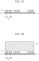
- FIG. 2A is a cross-sectional arrow view illustrating a cross-section of the optical sensor sheet 2 taken along line A-A in FIG. 1 .
- FIG. 2B is a cross-sectional arrow view illustrating a cross-section of the optical sensor sheet 2 on which a specimen 100 is disposed taken along line A-A in FIG. 1 .
- each of the plurality of optical sensor chips 21 k is attached to the sheet member 23 by an adhesive layer 24.
- the optical sensor chips 21 k adjacent to each other in the direction in which the plurality of optical sensor chips 21 k are continuous are connected by the optical fiber 22A and the optical fiber 22B.
- the specimen 100 is disposed on the optical sensor chip 21 k .
- the optical sensor chip 21 k includes, for example, an optical waveguide manufactured using microfabrication technology represented by silicon photonics technology.
- the optical sensor chip 21 k changes at least one of the intensity, the phase, or the frequency of an optical signal depending on the state of the specimen 100.
- FIG. 3 is a block diagram illustrating a configuration of the optical sensor sheet 2.
- Z optical sensor chips 21 k are continuously connected in the optical sensor sheet 2.
- optical sensor chips from the optical sensor chip 21 1 to an optical sensor chip 21z-i each include a spot-size converter unit 2101, a changer unit 2102, a spot-size converter unit 2103, a waveguide 2104A, and a waveguide 2104B.
- the optical sensor chip 21z includes the spot-size converter unit 2101, the changer unit 2102, the waveguide 2104A, the waveguide 2104B, and an optical path folding unit 2105.
- the spot-size converter unit 2101 and the spot-size converter unit 2103 are optical elements that convert the spot size, which is the magnitude of the spread of the light distribution in the optical fiber, and the spot size in the waveguide.
- the spot-size converter unit 2101 and the spot-size converter unit 2103 are implemented by, for example, a spot size converter including a waveguide.
- the waveguide is, for example, a silicon waveguide.
- the spot-size converter unit 2101 converts the spot size of an optical signal propagated through the optical fiber 22A on the basis of the waveguide 2104A, and outputs the optical signal with the converted spot size to the waveguide 2104A.
- the spot-size converter unit 2101 converts the spot size of an optical signal propagated through the waveguide 2104B on the basis of the optical fiber 22B, and outputs the optical signal with the converted spot size to the optical fiber 22B.
- the spot-size converter unit 2103 converts the spot size of an optical signal propagated through the waveguide 2104A on the basis of the optical fiber 22A, and outputs the optical signal with the converted spot size to the optical fiber 22A. In addition, the spot-size converter unit 2103 converts the spot size of an optical signal propagated through the optical fiber 22B on the basis of the waveguide 2104B, and outputs the optical signal with the converted spot size to the waveguide 2104B.
- the changer unit 2102 changes the characteristics of the input optical signal depending on the state of the specimen 100, and outputs the optical signal with the changed characteristics to the outside.
- the characteristics of the optical signal include an intensity characteristic, a phase characteristic, or a frequency characteristic of the optical signal.
- the changer unit 2102 may change at least one of the intensity characteristic, the phase characteristic, or the frequency characteristic of the input optical signal.
- the changer unit 2102 is implemented by, for example, a ring resonator including an optical waveguide. It is not limited to the ring resonator, and the changer unit 2102 is only required to change the characteristics of the optical signal depending on the state of the specimen 100, and may be a phase shifter including an optical waveguide, a frequency shifter including an optical waveguide, or an optical element including a combination of the phase shifter and the frequency shifter.
- the changer unit 2102 may be a ring resonator, a Mach-Zehnder interferometer (MZI), or a combination thereof. Even the changer unit 2102 configured as described above can change the characteristics of the optical signal depending on the state of the specimen 100.
- MZI Mach-Zehnder interferometer
- a plurality of the changer units 2102 may be provided in one optical sensor chip, and the plurality of changer units 2102 may change the characteristics of the input optical signal depending on a plurality of mutually different states of the specimen 100.
- a certain changer unit 2102 changes the characteristics of the input optical signal depending on the temperature of the specimen 100
- another changer unit 2102 changes the characteristics of the input optical signal depending on the moisture concentration of the specimen 100
- still another changer unit 2102 changes the characteristics of the input optical signal depending on the pressure applied from the specimen 100.
- the optical sensor chip configured as described above can change the characteristics of the input optical signal depending on a plurality of mutually different states of the specimen 100.
- the waveguide 2104A and the waveguide 2104B are thin wire waveguides that optically connect the spot-size converter unit 2101 and the changer unit 2102, and propagate an optical signal with the converted spot size.
- the waveguide 2104A propagates an optical signal from the optical sensor chip 21 1 to the optical sensor chip 21z.
- the waveguide 2104B propagates an optical signal from the optical sensor chip 21z to the optical sensor chip 21 1 .
- the optical path folding unit 2105 is a reflector unit for reflecting the optical signal whose characteristics have been changed by the changer unit 2102 to the optical sensor chip 21z-i at the preceding stage.
- the optical path folding unit 2105 is implemented by a loop mirror.
- the optical signal reflected by the optical path folding unit 2105 is sequentially propagated through Z optical sensor chips 21 k continuously connected in the optical sensor sheet 2, and is output from the optical sensor chip 21 1 to the optical transceiver unit 3.
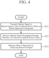
- FIG. 4 is a flowchart illustrating a measurement method according to the first embodiment, and illustrates the measurement method of the state of the specimen 100 using the optical sensor sheet 2.
- the optical transceiver unit 3 transmits an optical signal to the optical sensor chip 21 1 in the optical sensor sheet 2 on which the specimen 100 is disposed (step ST1).
- the optical transceiver unit 3 receives an optical signal that has reciprocated between Z optical sensor chips 21 k from the optical sensor chip 21 1 , and outputs the received signal to the received signal analyzer unit 4 (step ST2).
- the received signal analyzer unit 4 measures the state of the specimen 100 by analyzing the signal input from the optical transceiver unit 3 (step ST3).
- FIG. 5 is a flowchart illustrating details of the measurement method according to the first embodiment.
- the optical transceiver unit 3, the received signal analyzer unit 4, and the display unit 5 are included in a measurement device provided separately from the optical sensor sheet 2.
- the display of information by the display unit 5 means that information is displayed on a display included in the measurement device.
- the optical transmitter 31 included in the optical transceiver unit 3 generates an optical signal using light emitted from a light source and transmits the generated optical signal to the optical sensor chip 21 1 (step ST1a).
- the transmission of the optical signal means that the optical signal is output from the optical transmitter 31 to the optical fiber 22A, and the optical sensor chip 21 1 receives the optical signal propagated through the optical fiber 22A.
- a wavelength in the absorption wavelength band of water is set in each of the plurality of optical sensor chips 21 k .
- the optical transmitter 31 transmits an optical pulse signal in which Z wavelengths set in the Z optical sensor chips 21 k are multiplexed to the optical sensor chip 21 1 .
- the optical signal input to the optical sensor chip 21 1 sequentially propagates through the changer unit 2102 included in each of the optical sensor chips 21 k from the optical sensor chip 21 1 to the optical sensor chip 21z (step ST2a).
- the optical signal reaches the optical sensor chip 21z, the optical signal is reflected to the side of the optical sensor chip 21 1 by the optical path folding unit 2105 (step ST3a).
- the reflected optical signal sequentially propagates through the changer unit 2102 included in each of the optical sensor chips 21 k from the optical sensor chip 21z to the optical sensor chip 21 1 (step ST4a).
- the characteristics of the optical signal are changed depending on the state of the specimen 100 in the changer unit 2102 included in each of the optical sensor chips 21 k .
- the optical signal component having the wavelength in the absorption wavelength band of water in the wavelength-multiplexed optical signal is absorbed by water present inside or around the specimen 100, and the intensity thereof changes.
- the optical receiver 32 included in the optical transceiver unit 3 receives an optical signal from the optical sensor chip 21 1 (step ST5a).
- the reception of the optical signal means that the optical signal output from the optical sensor chip 21 1 to the optical fiber 22B is converted into an electrical signal by the light receiving element, and the electrical signal is input to the optical receiver 32.
- the received signal analyzer unit 4 measures the state of the specimen 100 by analyzing the signal input from the optical transceiver unit 3 (step ST6a).
- the received signal analyzer unit 4 calculates a reciprocating propagation time of a pulse using the pulse of a transmitted optical signal and the pulse of an input optical signal, and specifies the position of the optical sensor chip 21 k on the basis of the reciprocating propagation time.
- the received signal analyzer unit 4 calculates the difference between pulse peak values of the pulse of the transmitted optical signal and the pulse of the input optical signal, and measures a moisture content inside or around the specimen 100 for each optical sensor chip 21 k using a value of the calculated difference.
- the intensity of the optical signal decreases in proportion to the moisture content.
- the difference between the pulse peak values of the pulse of the transmitted optical signal and the pulse of the input optical signal is the amount of change in the intensity of the optical signal component with a wavelength assigned to the optical sensor chip 21 k .
- the display unit 5 receives measurement results of the state of the specimen from the received signal analyzer unit 4, and displays the received measurement results (step ST7a).
- the received signal analyzer unit 4 can measure the two-dimensional distribution of the moisture content in the specimen 100 by specifying the position of the optical sensor chip 21 k on the optical sensor sheet 2.
- the display unit 5 can graphically display the two-dimensional distribution of the moisture content of the specimen 100.
- a different resonance frequency is set in each of the plurality of optical sensor chips 21 k . That is, the optical sensor chip 21 k is configured to resonate at an individually set frequency.
- the waveguide is distorted and resonance conditions change.
- the ratio of the optical signal resonated at the frequency set in the optical sensor chip 21 k changes.
- the two-dimensional distribution of the pressure from the specimen 100 can be measured by specifying the position of the optical sensor chip 21 k on the optical sensor sheet 2.
- the display unit 5 can graphically display the two-dimensional distribution of the pressure from the specimen 100.
- FIG. 6 is a configuration diagram illustrating a changer unit 2102A that is a first modification of the changer unit 2102.
- the changer unit 2102A is a ring resonator.
- the ring resonator includes a waveguide 2106 with a ring shape.
- a resonance wavelength based on a curvature radius R and a waveguide effective refractive index n eff of the waveguide 2106 is set in the changer unit 2102A.
- the waveguide effective refractive index n eff can be changed by disposing a micro-heater on the waveguide 2106 or stacking a different magnetic body other than silicon.
- a different resonance wavelength ⁇ k is set in each of the changer units 2102A individually included in the Z optical sensor chips 21 k .
- the setting of the resonance wavelength ⁇ k means that the waveguide 2106 is configured with the curvature radius R and the waveguide effective refractive index n eff that cause it to resonate at the wavelength ⁇ k .
- the wavelength ⁇ k in the absorption wavelength band of water is set in the changer unit 2102A included in each of the Z optical sensor chips 21 k . That is, the wavelength ⁇ 1 is set in the changer unit 2102A included in the optical sensor chip 21 1 , the wavelength ⁇ k is set in the changer unit 2102A included in the optical sensor chip 21 k , and the wavelength ⁇ Z is set in the changer unit 2102A included in the optical sensor chip 21z.
- a region B surrounded by a broken line in FIG. 6 is a region where the waveguide 2104A and the waveguide 2106 are close to each other.
- the optical signal component with the wavelength ⁇ k propagates through the waveguide 2106 in the region B, and the optical signal component with the wavelength ⁇ ( ⁇ ⁇ k ) other than the wavelength ⁇ k directly propagates through the waveguide 2104A and is emitted from the changer unit 2102A.
- the optical signal with the wavelength ⁇ k resonates while circulating in the waveguide 2106, and is transmitted to the specimen 100 disposed on the waveguide 2106 or to the periphery of the specimen 100 close to the waveguide 2106 during the resonance.
- the transmitted optical signal component with the wavelength ⁇ k is absorbed by the water, so that the intensity of the optical signal with the wavelength ⁇ k decreases in proportion to the moisture content.
- the received signal analyzer unit 4 can measure the moisture content of the specimen 100 by analyzing the change in the intensity of the optical signal.
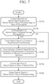
- FIG. 7 is a flowchart illustrating an operation of the optical sensor chip 21 k including the changer unit 2102A, and illustrates a case where moisture inside or around the specimen 100 is detected using the optical sensor sheet 2.
- the optical transceiver unit 3 transmits an optical signal in which the wavelengths ⁇ 1 to ⁇ Z set in Z optical sensor chips 21 k are multiplexed to the optical sensor chip 21 1 .
- the optical signal transmitted to the optical sensor chip 21 1 propagates sequentially from the optical sensor chip 21 1 to the optical sensor chip 21z.
- the spot-size converter unit 2101 included in the optical sensor chip 21 k converts the spot size of the optical signal output from the optical sensor chip at the preceding stage on the basis of the waveguide 2104A (step ST1b).
- the optical signal having the spot size converted and having propagated through the waveguide 2104A is incident on the changer unit 2102A.
- the waveguide 2106 which is a ring resonator, specifies whether or not the optical signal incident on the changer unit 2102A is a signal component with the wavelength ⁇ k and extracts the signal component (step ST2b).
- the signal component with the wavelength ⁇ k is extracted from the optical signal incident on the changer unit 2102A in the region B (step ST2b; YES)
- the extracted optical signal component circulates in the waveguide 2106 and resonates (step ST3b).
- the intensity of the signal component with the wavelength ⁇ k decreases in proportion to the moisture concentration (step ST4b).
- the signal component having circulated in the ring resonator reflects to the waveguide 2104A again and is emitted from the changer unit 2102A.
- the signal component with the wavelength ⁇ other than the wavelength ⁇ k is not extracted (step ST2b; NO) and the signal component with the wavelength ⁇ ( ⁇ ⁇ k ) directly propagates through the waveguide 2104A and is emitted from the changer unit 2102A.
- the spot-size converter unit 2103 converts the spot size of the optical signal emitted from the changer unit 2102A on the basis of the optical fiber 22A (step ST5b).
- the optical signal with the converted spot size is output to the optical sensor chip 21 k at the subsequent stage through the optical fiber 22A (step ST6b).
- the optical signal sequentially propagated from the optical sensor chip 21 1 to the optical sensor chip 21z is reflected at the optical sensor chip 21z, and is sequentially propagated from the optical sensor chip 21z to the optical sensor chip 21 1 .
- step ST1b the spot-size converter unit 2103 converts the spot size of the optical signal output from the optical sensor chip at the preceding stage on the basis of the waveguide 2104B.
- step ST5b the spot-size converter unit 2101 converts the spot size of the optical signal emitted from the changer unit 2102A on the basis of the optical fiber 22B.
- step ST4b the signal component with the resonance wavelength ⁇ k set in the optical sensor chip 21 k circulates in the waveguide 2106 and resonates, and the intensity thereof decreases in proportion to the moisture content of the specimen 100.
- the signal component with the wavelength ⁇ ( ⁇ ⁇ k ) does not propagate through the waveguide 2106 but directly propagates through the waveguide 2104B and is emitted from the changer unit 2102A. That is, in the changer unit 2102A, the waveguide 2104B is provided close to the waveguide 2106, similarly to the waveguide 2104A illustrated in FIG. 6 .
- the optical signal propagating from the optical sensor chip 21z toward the optical sensor chip 21 1 may directly pass through the changer unit 2102A without propagating through the waveguide 2106.
- FIG. 8 is a graph illustrating a relationship between the wavelength and the intensity of an optical signal propagating through the changer unit 2102 included in the optical sensor chip 21 k of the optical sensor sheet 2 on which the specimen 100 is not disposed.
- the horizontal axis represents the wavelength of the optical signal
- the vertical axis represents the intensity of the optical signal. Since the specimen 100 is not disposed and there is no absorption of water present inside or around the specimen 100, the intensities of Z optical signals with the wavelengths ⁇ 1 to ⁇ Z in the absorption wavelength band of water are constant at an intensity P 0 .
- FIG. 9 is a graph illustrating a relationship between the wavelength and the intensity of an optical signal propagating through the changer unit 2102 included in the optical sensor chip 21 k of the optical sensor sheet 2 on which the specimen 100 is disposed.
- the horizontal axis represents the wavelength of the optical signal
- the vertical axis represents the intensity of the optical signal.
- the signal component with the wavelength ⁇ 2 has an intensity P 1 lower than the intensity P 0 when the specimen 100 is not disposed, and the signal component with the wavelength ⁇ k has an intensity P 2 lower than the intensity P 0 .
- the signal component with the resonance wavelength ⁇ 2 set in the optical sensor chip 21 2 is absorbed by moisture present inside or around the specimen 100, and the signal component with the resonance wavelength ⁇ k set in the optical sensor chip 21 k is absorbed by moisture present inside or around the specimen 100.
- the received signal analyzer unit 4 can measure the moisture content inside or around the specimen 100 by analyzing the amount of change (P 0 -P 1 and P 0 -P 2 ) in the intensity of the signal component with the resonance wavelength ⁇ k set in each of the Z optical sensor chips 21 k .
- FIG. 10 is a graph illustrating a relationship between the position of the optical sensor chip 21 k of the optical sensor sheet 2 on which the specimen 100 is disposed and the moisture content of the specimen 100.
- the received signal analyzer unit 4 calculates the reciprocating propagation time of a pulse using the pulse of an optical signal transmitted to the optical sensor chip 21 1 and the pulse of an optical signal received from the optical sensor chip 21 1 , and specifies the position of the optical sensor chip 21 k in the XY coordinate system on the optical sensor sheet 2 on the basis of the reciprocating propagation time.
- the received signal analyzer unit 4 measures the moisture content of the specimen 100 at each position of the optical sensor chip 21 k , and outputs information indicating the moisture content at each position of the optical sensor chip 21 k to the display unit 5 as measurement results.
- the display unit 5 displays a three-dimensional graph illustrating the moisture content of the specimen 100 at each position of the optical sensor chip 21 k in the XY coordinate system on the optical sensor sheet 2.
- the Z optical sensor chips 21 k may change the characteristics of the input optical signal depending on a plurality of types of states of the specimen 100.
- the Z optical sensor chips 21 k may include an optical sensor chip that changes the characteristics of the optical signal depending on the temperature of the specimen 100, an optical sensor chip that changes the characteristics of the optical signal depending on the moisture content of the specimen 100, and an optical sensor chip that changes the characteristics of the optical signal depending on the pressure from the specimen 100.
- a part of the Z optical sensor chips 21 k may be optical sensor chips that change the characteristics of the optical signal depending on the moisture content of the specimen 100, and the remaining may be optical sensor chips that change the characteristics of the optical signal depending on the temperature of the specimen 100.
- the changer unit 2102A may include a ring resonator that changes the characteristics of the optical signal depending on the moisture content of the specimen 100 and a ring resonator that changes the characteristics of the optical signal depending on the temperature of the specimen 100.
- the characteristics of the optical signal input to one optical sensor chip can be changed depending on a plurality of types of states of the specimen 100.
- the optical sensor sheet 2 may be a sheet in which a plurality of units including a plurality of optical sensor chips that change the characteristics of the optical signal depending on each of a plurality of types of states of the specimen 100 are continuously connected.
- a plurality of units including a plurality of optical sensor chips that change the characteristics of the optical signal depending on each of a plurality of types of states of the specimen 100 are continuously connected.
- an optical sensor chip that detects the temperature of the specimen 100, an optical sensor chip that detects the moisture content of the specimen 100, and an optical sensor chip that detects the pressure from the specimen 100 are optically connected via the optical fiber 22, and a plurality of such units are continuously connected in the optical sensor sheet 2.
- the waveguide 2106 in which the effective curvature radius R changes with a temperature change ⁇ T is used in the changer unit 2102A.
- the waveguide 2106 satisfying 2 ⁇ ⁇ ⁇ R ⁇ n eff m ⁇ ⁇ , which is a relational expression indicating the correspondence relationship between the amount of change ⁇ R in curvature radius and the amount of shift ⁇ in resonance wavelength, is used.
- the received signal analyzer unit 4 calculates the amount of change ⁇ R in the curvature radius of the waveguide 2106 on the basis of the amount of shift ⁇ of the resonance wavelength between a transmitted signal and a received signal, and calculates the temperature change ⁇ T using ⁇ R.
- FIG. 11 is a block diagram illustrating a first configuration example of a measurement device, in which a modulated signal generator unit 6 is added to the measurement device illustrated in FIG. 1 .
- the modulated signal generator unit 6 generates a modulated signal used for measuring the state of the specimen 100.
- the modulated signal is a phase modulated signal or a frequency modulated signal.
- the optical transmitter 31 included in the optical transceiver unit 3 transmits, to the optical sensor chip 21 1 , an optical signal modulated using the modulated signal generated by the modulated signal generator unit 6 as a carrier wave.
- the modulated signal generator unit 6 outputs a phase-modulated pulse signal to the optical transmitter 31 on the basis of the time of flight (ToF) LiDAR system.
- the pulse signal reciprocates between the optical sensor chip 21 1 and the optical sensor chip 21z.
- the received signal analyzer unit 4 calculates a correlation value between the pulse of the received signal received from the optical sensor chip 21 1 by the optical receiver 32 and the pulse of the transmitted signal, and measures the state of the specimen 100 on the basis of the calculated correlation value.
- the measurement results by the received signal analyzer unit 4 are displayed on the display unit 5.
- FIG. 12 is a configuration diagram illustrating a measurement system 1A that is a first modification of the measurement system 1.
- the optical sensor sheet 2 is laid on a bed 200, and the specimen is a person 100A lying on the bed 200.
- the person 100A lying on the bed 200 the person 100A is disposed on the optical sensor sheet 2.
- the measurement system 1A measures the state of the person 100A lying on the bed 200.
- the received signal analyzer unit 4 can measure the temperature, the amount of perspiration, or the sleeping position of the person 100A on the basis of the change in the characteristics of the optical signal for each optical sensor chip 21 k of the optical sensor sheet 2. For example, the received signal analyzer unit 4 measures the amount of perspiration of the person 100A and the temporal change thereof at each position of the optical sensor chip 21 k , and outputs the measurement results to the display unit 5. As a result, the display unit 5 can graphically display the temporal change in the distribution of the amount of perspiration of the person 100A.
- FIG. 13 is a configuration diagram illustrating a measurement system 1B that is a second modification of the measurement system 1.
- the optical sensor sheet 2 is buried in a farmland, and the specimen is farmland soil 100B.
- the measurement system 1B measures the state of the farmland soil.
- the received signal analyzer unit 4 measures the temperature, the moisture content, or the nutrient component of the soil 100B on the basis of the change in the characteristics of an optical signal for each optical sensor chip 21 k of the optical sensor sheet 2.
- the wavelength ⁇ k in the absorption wavelength band of carbon dioxide or calcium is set in the changer unit 2102A included in each of Z optical sensor chips 21 k .
- the intensity of the optical signal circulated in a ring resonator and resonated decreases depending on the carbon dioxide concentration or the calcium concentration of the soil 100B.
- the received signal analyzer unit 4 measures the temperature, the moisture content, or the nutrient component of the soil 100B and the temporal change thereof at each position of the optical sensor chip 21 k , on the basis of the temporal change in the intensity of the optical signal, and outputs the measurement results to the display unit 5.
- the display unit 5 can graphically display the temporal change in the distribution of the temperature, the moisture content, or the nutrient component of the soil 100B.
- FIG. 14 is a configuration diagram illustrating a changer unit 2102B that is a second modification of the changer unit 2102.
- the changer unit 2102B is obtained by adding a waveguide 2107 to the changer unit 2102A.
- the waveguide 2107 includes a band-like line path provided close to the waveguide 2106 which is a ring resonator and a ring-like line path provided at an end thereof.
- the optical signal component with the resonance wavelength ⁇ k propagates from the waveguide 2104A to the waveguide 2106 and resonates, then propagates through the waveguide 2107, and the optical path is reflected in a direction indicated by an arrow C. As illustrated in FIG. 14 , the reflected optical signal component propagates through the waveguide 2106 again and resonates, and then propagates through the waveguide 2104A toward the optical transceiver unit 3 as the emitted light with the wavelength ⁇ k .
- FIG. 15 is a configuration diagram illustrating a changer unit 2102C that is a third modification of the changer unit 2102.
- the changer unit 2102B is an optical element that outputs a part of the optical signal propagating through the waveguide 2104A to the outside, and receives reflected light obtained by reflecting the light output to the outside.
- the changer unit 2102B is implemented by a grating coupler.
- the characteristics of the optical signal emitted from the changer unit 2102B are changed depending on the state of the specimen 100 outside, and the optical signal is reflected by the specimen 100, and input to the changer unit 2102B again.
- the optical signal whose characteristics have been changed depending on the state of the specimen 100 propagates through the waveguide 2104A and is output to the spot-size converter unit 2103.
- FIG. 16 is a block diagram illustrating a second configuration example of the measurement device.
- the measurement device includes an optical transceiver unit 3A, the received signal analyzer unit 4, the display unit 5, and the modulated signal generator unit 6.
- the optical transceiver unit 3A includes the optical transmitter 31, the optical receiver 32, an optical splitter 33, and an optical multiplexer 34.
- the modulated signal generator unit 6 outputs a frequency modulated signal such as a chirped sine wave to the optical transmitter 31 included in the optical transceiver unit 3A on the basis of the frequency-modulated-continuous-wave (FMCW) LiDAR system.
- the optical transmitter 31 outputs a modulated optical signal to the optical splitter 33 using the frequency modulated signal generated by the modulated signal generator unit 6 as a carrier wave.
- the optical splitter 33 splits the optical signal generated by the optical transmitter 31 to the optical sensor chip 21 1 and the optical multiplexer 34.
- the optical transmitter 31 transmits the optical signal split by the optical splitter 33 to the optical sensor chip 21 1 via the optical fiber 22A.
- the optical signal reciprocates between the optical sensor chip 21 1 and the optical sensor chip 21z.
- the optical multiplexer 34 multiplexes the optical signal received from the optical sensor chip 21 1 via the optical fiber 22B and the transmitting optical signal split by the optical splitter 33, and outputs the multiplexed optical signal to the optical receiver 32.
- the received signal analyzer unit 4 performs Fourier analysis on the received signal received from the optical sensor chip 21 1 by the optical receiver 32, thereby calculating the amount of change in amplitude and the amount of frequency shift between the transmitted signal and the received signal, and measures the state of the specimen 100 on the basis of the calculated amount of change in amplitude and amount of frequency shift. The measurement results are displayed on the display unit 5.
- FIG. 17 is a block diagram illustrating a third configuration example of the measurement device.
- the measurement device includes an optical transceiver unit 3B, the received signal analyzer unit 4, the display unit 5, and the modulated signal generator unit 6.
- the optical transceiver unit 3B includes the optical transmitter 31, the optical receiver 32, and an optical circulator 35.
- the optical circulator 35 switches the output destination of the optical signal input from the optical transmitter 31 to the optical fiber 22A, and switches the output destination of the optical signal from the optical fiber 22B to the optical receiver 32.
- the optical fiber 22A and the optical fiber 22B can be shared by one optical fiber.
- the ring resonator illustrated in FIGS. 6 and 14 may be replaced with an optical element having a phase shifter function or a frequency shifter function, or the ring resonator may have the phase shifter function or the frequency shifter function.
- a member formed of a material different from that of the waveguide 2106 is stacked on the waveguide 2106 which is a ring resonator.
- the changer unit 2102A changes the characteristics of the optical signal depending on the material of the member stacked on the waveguide 2106.
- the phase of the optical signal circulated in the waveguide 2106 changes in proportion to the intensity of the magnetic field generated around the waveguide 2106.
- the waveguide effective refractive index n eff of the waveguide 2106 also changes depending on the change in the phase of the optical signal.
- the received signal analyzer unit 4 calculates the amount of change ⁇ n eff in the waveguide effective refractive index of the waveguide 2106 using the calculated amount of shift ⁇ in resonance wavelength, and calculates the intensity of the magnetic field using the calculated ⁇ n eff .
- the optical sensor chip 21 k can detect the magnetic field from the specimen 100.
- the waveguide 2106 may be a waveguide on which a member that changes the waveguide effective refractive index n eff by binding to DNA such as graphene is stacked.
- DNA is present around the waveguide 2106
- the phase of the optical signal circulated in the waveguide 2106 changes.
- the waveguide effective refractive index n eff of the waveguide 2106 also changes depending on the change in the phase of the optical signal.
- the received signal analyzer unit 4 calculates the amount of change ⁇ n eff in the waveguide effective refractive index of the waveguide 2106 using the amount of shift ⁇ in resonance wavelength, and calculates the binding amount of DNA using the calculated ⁇ n eff .
- the optical sensor chip 21 k can detect the DNA of the specimen 100.
- the functions of the optical transceiver unit 3, the received signal analyzer unit 4, the display unit 5, and the modulated signal generator unit 6 in the measurement device illustrated in FIG. 11 are implemented by a processing circuitry. That is, the measurement device includes a processing circuitry for performing the processing from step ST1 to step ST3 illustrated in FIG. 4 .
- the processing circuitry may be dedicated hardware, or may be a central processing unit (CPU) that executes a program stored in a memory.
- FIG. 18A is a block diagram illustrating a hardware configuration that implements the functions of the measurement device illustrated in FIG. 11 .
- FIG. 18B is a block diagram illustrating a hardware configuration that executes software that implements the functions of the measurement device illustrated in FIG. 11 .
- an input interface 1000 is an interface that relays an electrical signal corresponding to a signal from the optical sensor sheet 2.
- An output interface 1001 is an interface that relays measurement result information output to the display.
- the processing circuitry is a processing circuitry 1002 of dedicated hardware illustrated in FIG. 18A
- the processing circuitry 1002 corresponds to, for example, a single circuit, a composite circuit, a programmed processor, a parallel programmed processor, an application specific integrated circuit (ASIC), a field-programmable gate array (FPGA), or a combination thereof.
- the functions of the optical transceiver unit 3, the received signal analyzer unit 4, the display unit 5, and the modulated signal generator unit 6 in the measurement device may be implemented by separate processing circuitries, or these functions may be collectively implemented by one processing circuitry.
- the processing circuitry is a processor 1003 illustrated in FIG. 18B
- the functions of the optical transceiver unit 3, the received signal analyzer unit 4, the display unit 5, and the modulated signal generator unit 6 are implemented by software, firmware, or a combination of software and firmware. Note that the software or firmware is described as a program and stored in a memory 1004.
- the processor 1003 reads and executes the program stored in the memory 1004, thereby implementing the functions of the optical transceiver unit 3, the received signal analyzer unit 4, the display unit 5, and the modulated signal generator unit 6 in the measurement device.
- the measurement device includes the memory 1004 for storing a program that allows the processing from step ST1 to step ST3 in the flowchart illustrated in FIG. 4 to be performed when executed by the processor 1003.
- These programs cause a computer to execute procedures or methods of processing performed by the optical transceiver unit 3, the received signal analyzer unit 4, the display unit 5, and the modulated signal generator unit 6.
- the memory 1004 may be a computer-readable storage medium that stores a program for causing a computer to function as the optical transceiver unit 3, the received signal analyzer unit 4, the display unit 5, and the modulated signal generator unit 6.
- the memory 1004 corresponds, for example, to a nonvolatile or volatile semiconductor memory such as a random access memory (RAM), a read only memory (ROM), a flash memory, an erasable programmable read only memory (EPROM), or an electrically-EPROM (EEPROM), a magnetic disk, a flexible disk, an optical disk, a compact disk, a mini disk, a DVD, or the like.
- RAM random access memory
- ROM read only memory
- EPROM erasable programmable read only memory
- EEPROM electrically-EPROM
- optical transceiver unit 3 the received signal analyzer unit 4, the display unit 5, and the modulated signal generator unit 6 in the measurement device may be implemented by dedicated hardware, and some of the functions may be implemented by software or firmware.
- the functions of the optical transceiver unit 3 and the received signal analyzer unit 4 are implemented by the processing circuitry 1002 that is dedicated hardware, and the functions of the display unit 5 and the modulated signal generator unit 6 are implemented by the processor 1003 reading and executing the program stored in the memory 1004.
- the processing circuitry can implement the functions by hardware, software, firmware, or a combination thereof.
- the optical sensor sheet 2 includes Z optical sensor chips 21 k that change the characteristics of an input optical signal depending on the state of the specimen 100 and output the optical signal with the changed characteristics, the optical fiber 22 that propagates the optical signal input to and output from the Z optical sensor chips 21 k , and the sheet member 23 including the Z optical sensor chips 21 k .
- the optical sensor device Since the optical signal is input and output between the optical sensor chip 21 k and the optical sensor chip 21 k-1 through the optical fiber 22, the optical sensor device according to the first embodiment can detect the state of the specimen without using an electric signal for a specimen-state detection signal and without providing a sensor circuit unit for each sensor chip. As a result, power consumption is reduced as compared with the sensor described in Patent Literature 1.
- the Z optical sensor chips 21 k are provided on the sheet member 23, and change the characteristics of the input optical signal depending on the state of the specimen 100 disposed on the sheet member 23 or the specimen 100 disposed around the sheet member 23. Even in the optical sensor sheet 2 configured as described above, it is possible to detect the state of the specimen without using an electric signal for a specimen-state detection signal and without providing a sensor circuit unit for each sensor chip. Note that, by meandering the Z optical sensor chips 21 k connected via the optical fiber 22, the optical sensor chips 21 k can be provided on the sheet member 23 with various shapes, and the degree of freedom in the arrangement of the optical sensor chips 21 k is high, and the arrangement density is improved. As a result, the optical sensor sheet 2 can be disposed even in a narrow space in which the optical sensor sheet is conventionally difficult to be disposed.
- the Z optical sensor chips 21 k change the characteristics of the input optical signal depending on the state of the specimen 100 disposed on the sheet member 23 or disposed around the sheet member 23. Since the state of the specimen 100 can be detected at each position of the optical sensor chip 21 k , the measurement range of the state of the specimen 100 is extended.
- the Z optical sensor chips 21 k change the characteristics of the input optical signal depending on a plurality of types of states of the specimen 100. Since the plurality of types of states of the specimen 100 can be detected for each optical sensor chip 21 k , the measurement range of the state of the specimen 100 is extended.
- the changer unit 2102A changes the characteristics of the optical signal depending on the material of the member stacked on the waveguide 2106. Since the plurality of types of states of the specimen 100 can be detected for each optical sensor chip 21 k , the measurement range of the state of the specimen 100 is extended.
- the measurement system 1 includes the optical sensor sheet 2, the optical transceiver unit 3 that transmits an optical signal to the optical sensor chip 21 k in the optical sensor sheet 2 and receives an optical signal propagated through the Z optical sensor chips 21 k provided continuously in the optical sensor sheet 2, and the received signal analyzer unit 4 that measures the state of the specimen 100 by analyzing a signal received by the optical transceiver unit 3. Since the received signal analyzer unit 4 measures the state of the specimen 100 for each optical sensor chip 21 k , the measurement range of the state of the specimen 100 is extended.
- the measurement system 1 includes the modulated signal generator unit 6 that generates a modulated signal used for measuring the state of the specimen 100.
- the optical transceiver unit 3 modulates an optical signal using the modulated signal generated by the modulated signal generator unit 6, and transmits the modulated optical signal to the optical sensor chip 21 1 .
- FIG. 19 is a configuration diagram illustrating a measurement system 1C according to a second embodiment. While the measurement systems 1, 1A, and 1B according to the first embodiment use the optical sensor sheet 2 disposed two-dimensionally, the measurement system 1C uses the optical sensor sheet 2 disposed three-dimensionally in a closed space. For example, by providing the optical sensor sheet 2 in such a manner as to cover a columnar specimen 100C, the measurement system 1C can determine the entire specimen 100C as a measurement portion, and the measurement range is extended.
- the optical sensor sheet 2 is provided in such a manner as to cover the columnar specimen 100C, the optical sensor sheet 2 is attached to all the inner wall surfaces of a box 400.
- the optical sensor sheet 2 can detect the state of the specimen 100C.
- the entire specimen 100C can be determined as a measurement portion by three-dimensionally disposing the optical sensor sheet 2 in the closed space as illustrated in FIG. 19 .
- the box 400 does not need to be a closed space.
- the optical sensor sheet 2 may be three-dimensionally disposed in a space where a part is opened, such as a pipe or a tunnel. In this case, the optical sensor sheet 2 cannot be disposed in the opened portion, but the optical sensor sheet 2 can be disposed around the specimen 100C except for this portion. Therefore, the optical sensor system 1C can determine all the portions of the specimen 100C facing the optical sensor sheet 2 as measurement portions.
- the closed space is a cardboard box including the optical sensor sheet 2 on the inner wall surface
- a food is disposed as the specimen 100C inside the cardboard box
- the optical sensor chip 21 k is, for example, an optical sensor chip that detects the moisture content of the food or the humidity inside the cardboard box.
- the measurement system 1C can measure the moisture distribution of the food or the humidity distribution of the food inside the cardboard box using the optical sensor sheet 2.
- a food manager can recognize the temporal change in the moisture distribution of the food or the humidity distribution of the food on the basis of the measurement results of the moisture distribution of the food or the humidity distribution of the food.
- the measurement results can also be used to predict the occurrence of rotting of the food.
- the closed space may be a bathroom including the optical sensor sheet 2 on the wall surface, and the atmosphere inside the bathroom may be the specimen 100C.
- the optical sensor chip 21 k provided inside the bathroom is, for example, an optical sensor chip that detects the humidity of the atmosphere inside the bathroom.
- the measurement system 1C measures the humidity distribution of the atmosphere inside the bathroom using the optical sensor sheet 2. As a result, the temporal change in the humidity distribution of the atmosphere inside the bathroom can be recognized. In addition, the measurement results of the humidity distribution of the atmosphere inside the bathroom can also be used to predict the occurrence of mold on the bathroom wall surface.
- the optical sensor sheet 2 is provided in such a manner as to cover the specimen 100C.
- the measurement system 1C can determine the entire specimen 100C as a measurement portion, and the measurement range is extended.
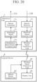
- FIG. 20 is a block diagram illustrating a configuration of a measurement device according to a third embodiment.
- the measurement device according to the third embodiment includes a transceiver unit 7 and an external device 8.
- the transceiver unit 7 and the external device 8 are configured to be capable of transmitting and receiving wireless signals.
- the transceiver unit 7 includes an optical transmitter 71, an optical receiver 72, a modulated signal generator unit 73, a modulation-demodulation control unit 74, a received signal analyzer unit 75, and a wireless signal transceiver unit 76.
- the transceiver unit 7 is an IoT sensor.
- the external device 8 includes a wireless signal transceiver unit 81, an optical-sensor control unit 82, and a display unit 83.
- the external device 8 is implemented by a mobile phone terminal, a smartphone, a personal digital assistant (PDA), or a personal computer (PC).
- PDA personal digital assistant
- PC personal computer
- the optical transmitter 71 transmits an optical signal to the optical sensor chip 21 1 through the optical fiber 22A.
- the optical receiver 72 receives an optical signal from the optical sensor chip 21 1 through the optical fiber 22B.
- the optical transmitter 71 generates a transmitting optical signal using light emitted from a light emitting element as a light source and the modulated signal generated by the modulated signal generator unit 73, and outputs the generated optical signal to the optical fiber 22A.
- the optical receiver 72 acquires an electrical signal converted from an optical signal by a light receiving element.
- the light emitting element and the light receiving element may be provided separately, or may be an optical sensor in which the light emitting element and the light receiving element are integrated into one.
- the optical transceiver unit including the optical transmitter 71 and the optical receiver 72 may be provided in an external device provided separately from the optical sensor sheet 2, or may be provided in the optical sensor sheet 2.
- the optical transceiver unit may be integrated on an InP substrate provided on the optical sensor sheet 2.
- the modulated signal generator unit 73 may generate a modulated signal to be used to measure a state designated by a control signal among a plurality of types of states of the specimen 100, and output the generated modulated signal to the optical transmitter 71.
- the optical transmitter 71 generates an optical signal to which modulation corresponding to the measurement of the state designated by the control signal has been applied.
- the modulated signal generator unit 73 generates a phase modulated signal in a case where the moisture content of the specimen 100 is designated by the control signal, and generates a frequency modulated signal in a case where the temperature of the specimen 100 is designated by the control signal.
- the modulation-demodulation control unit 74 demodulates the control signal received from the external device 8 by the wireless signal transceiver unit 76, and outputs the demodulated control signal to the modulated signal generator unit 73.
- the modulation-demodulation control unit 74 compensates for the degradation of the signal quality of the control signal wirelessly transmitted from the external device 8, and outputs the control signal in which the degradation of the signal quality has been compensated to the modulated signal generator unit 73.
- the modulation-demodulation control unit 74 compensates for the degradation of the signal quality by performing error detection of a signal being wirelessly transmitted and corrects the detected error.
- the received signal analyzer unit 75 measures the state of the specimen 100 by analyzing the optical signal received from the optical sensor chip 21 1 by the optical receiver 72.
- the optical sensor sheet 2 may be two-dimensionally disposed as described in the first embodiment, or may be three-dimensionally disposed as described in the second embodiment.
- the wireless signal transceiver unit 76 is a wireless communication unit for transmitting and receiving a wireless signal to and from the external device 8, and is implemented by, for example, a communication device that performs near field communication represented by Bluetooth (registered trademark) or a WiFi router.
- the wireless signal transceiver unit 76 transmits measurement result information measured by the received signal analyzer unit 75 to the external device 8.
- the wireless signal transceiver unit 81 is a wireless communication unit for transmitting and receiving a wireless signal to and from the transceiver unit 7, and is implemented by, for example, a communication device that performs near field communication represented by Bluetooth (registered trademark) or a WiFi router.
- the wireless signal transceiver unit 81 transmits a control signal from the optical-sensor control unit 82 to the transceiver unit 7, and receives measurement result information from the transceiver unit 7.
- the optical-sensor control unit 82 is a control unit that generates a control signal for designating the state of the specimen 100.
- the wireless signal transceiver unit 81 transmits the control signal generated by the optical-sensor control unit 82 to the wireless signal transceiver unit 76 by wireless communication.
- the display unit 83 displays information on a display mounted on the external device 8. For example, the display unit 83 causes the display to display the measurement result information received from the transceiver unit 7 by the wireless signal transceiver unit 81.
- the measurement device includes the wireless signal transceiver unit 76 that performs wireless communication with the external device 8 including the optical-sensor control unit 82 and the display unit 83.
- the wireless signal transceiver unit 76 transmits information of the measurement results measured by the received signal analyzer unit 75 to the external device 8.
- the display unit 83 displays the measurement result information.
- the optical-sensor control unit 82 generates a control signal for designating the state of the specimen 100.
- the modulated signal generator unit 73 generates a modulated signal to be used to measure the state of the specimen 100 designated by the control signal, and outputs the generated modulated signal to the optical transmitter 71.
- the user carrying the external device 8 can control the measurement of the state of the specimen 100 using the optical sensor sheet 2 and the transceiver unit 7 from a remote place.
- the optical sensor device according to the present disclosure can be used to measure the state of various specimens.
- 1, and 1A to 1C Measurement system
- 2 Optical sensor sheet
- 3A, and 3B Optical transceiver unit
- 4 and 75 Received signal analyzer unit
- 5 and 83 Display unit
- 6 and 73 Modulated signal generator unit
- 7 Transceiver unit
- 8 External device
- 21 1 , 21 2 , 21 k , 21 k-1 , 21 Z-1 , and 21z Optical sensor chip
- 22, 22A, and 22B Optical fiber
- 23 Sheet member
- 24 Adhesive layer
- 31 and 71 Optical transmitter
- 32 and 72 Optical receiver
- 33 Optical splitter
- 34 Optical multiplexer
- 35 Optical circulator
- 74 Modulation-demodulation control unit
- 76 and 81 Wireless signal transceiver unit
- 82 Optical-sensor control unit
- 100 and 100C Specimen
- 100A Person
- 100B Soil
- 200 Bed
- 400 Box
- 1000 Input
Landscapes
- Physics & Mathematics (AREA)
- Chemical & Material Sciences (AREA)
- Life Sciences & Earth Sciences (AREA)
- Health & Medical Sciences (AREA)
- Biochemistry (AREA)
- Pathology (AREA)
- Immunology (AREA)
- General Physics & Mathematics (AREA)
- General Health & Medical Sciences (AREA)
- Analytical Chemistry (AREA)
- Engineering & Computer Science (AREA)
- Spectroscopy & Molecular Physics (AREA)
- Chemical Kinetics & Catalysis (AREA)
- Plasma & Fusion (AREA)
- Botany (AREA)
- Medicinal Chemistry (AREA)
- Food Science & Technology (AREA)
- Wood Science & Technology (AREA)
- Investigating Or Analysing Materials By Optical Means (AREA)
- Optical Transform (AREA)
Abstract
Description
- The present disclosure relates to an optical sensor device, a measurement system, and a measurement method.
- In recent years, the technique of nondestructively measuring the state of a specimen has become widespread. For example, Patent Literature 1 describes a sensor that nondestructively measures a magnetic field based on a pulse signal of a specimen. This sensor includes a plurality of magnetic field sensors, and includes a sensor circuit unit for each magnetic field sensor. A magnetic-field detection signal is output from the magnetic field sensor to the sensor circuit unit via an electric wire.
- Patent Literature 1:
JP 2017-223570 A - In the sensor described in Patent Literature 1, the magnetic-field detection signal output from the magnetic field sensor is an electric signal, and the sensor circuit unit that measures the magnetic field of a specimen using the electric signal is provided for each magnetic field sensor. Therefore, the sensor described in Patent Literature 1 has a problem that power consumption is large.
- The present disclosure solves the above problems, and an object thereof is to obtain an optical sensor device, a measurement system, and a measurement method capable of detecting the state of a specimen without using an electric signal for a specimen-state detection signal and without providing a sensor circuit unit for each sensor chip.
- An optical sensor device according to the present disclosure includes: a plurality of optical sensor chips to change a characteristic of an input optical signal depending on a state of a specimen and to output an optical signal with a changed characteristic; an optical path through which an optical signal propagates, and via which the optical signal is input to and output from the plurality of optical sensor chips; and a chip holding member to which the plurality of optical sensor chips are provided.
- According to the present disclosure, the optical sensor device includes: a plurality of optical sensor chips to change a characteristic of an input optical signal depending on a state of a specimen and to output an optical signal with a changed characteristic; an optical path through which an optical signal propagates, and via which the optical signal is input to and output from the plurality of optical sensor chips; and a chip holding member to which the plurality of optical sensor chips are provided. Since the optical signal is input and output between the optical sensor chips through the optical path, the optical sensor device according to the present disclosure can detect the state of the specimen without using an electric signal for a specimen-state detection signal and without providing a sensor circuit unit for each sensor chip.
-
-
FIG. 1 is a configuration diagram illustrating a measurement system according to a first embodiment. -
FIG. 2A is a cross-sectional arrow view illustrating a cross-section of an optical sensor sheet taken along line A-A inFIG. 1 , andFIG. 2B is a cross-sectional arrow view illustrating a cross-section of the optical sensor sheet on which a specimen is disposed taken along line A-A inFIG. 1 . -
FIG. 3 is a block diagram illustrating a configuration of the optical sensor sheet. -
FIG. 4 is a flowchart illustrating a measurement method according to the first embodiment. -
FIG. 5 is a flowchart illustrating details of the measurement method according to the first embodiment. -
FIG. 6 is a configuration diagram illustrating a first modification of a changer unit. -
FIG. 7 is a flowchart illustrating an operation of an optical sensor chip including the changer unit ofFIG. 6 . -
FIG. 8 is a graph illustrating a relationship between the wavelength and the intensity of an optical signal propagating through the changer unit included in the optical sensor chip of the optical sensor sheet on which the specimen is not disposed. -
FIG. 9 is a graph illustrating a relationship between the wavelength and the intensity of an optical signal propagating through the changer unit included in the optical sensor chip of the optical sensor sheet on which the specimen is disposed. -
FIG. 10 is a graph illustrating a relationship between the position of the optical sensor chip of the optical sensor sheet on which the specimen is disposed and the moisture content of the specimen. -
FIG. 11 is a block diagram illustrating a first configuration example of a measurement device. -
FIG. 12 is a configuration diagram illustrating a first modification of the measurement system according to the first embodiment. -
FIG. 13 is a configuration diagram illustrating a second modification of the measurement system according to the first embodiment. -
FIG. 14 is a configuration diagram illustrating a second modification of the changer unit. -
FIG. 15 is a configuration diagram illustrating a third modification of the changer unit. -
FIG. 16 is a block diagram illustrating a second configuration example of the measurement device. -
FIG. 17 is a block diagram illustrating a third configuration example of the measurement device. -
FIG. 18A is a block diagram illustrating a hardware configuration for implementing the functions of the measurement device, andFIG. 18B is a block diagram illustrating a hardware configuration for executing software for implementing the functions of the measurement device. -
FIG. 19 is a configuration diagram illustrating a measurement system according to a second embodiment. -
FIG. 20 is a block diagram illustrating a configuration of a measurement device according to a third embodiment. -
FIG. 1 is a configuration diagram illustrating a measurement system 1 according to a first embodiment. InFIG. 1 , the measurement system 1 is a system that measures the state of a specimen using anoptical sensor sheet 2. The measurement system 1 can measure the state of a solid, liquid, or gas specimen, and the specimen may be a living body such as a human or an animal. The state of the specimen is a state where optical measurement by an optical sensor chip 21k provided in theoptical sensor sheet 2 can be performed, and is a state inside the specimen or a state around the specimen. The state of the specimen is, for example, a temperature inside or around the specimen, a moisture concentration of the specimen, or a pressure applied from the specimen. - The
optical sensor sheet 2 is an optical sensor device including a plurality of the optical sensor chips 21k, anoptical fiber 22, and asheet member 23, wherein "k" is any natural number equal to or more than 1 and equal to or less than Z, and inFIG. 1 , theoptical sensor sheet 2 includes Z optical sensor chips 21k. - The
sheet member 23 is a chip holding member including Z optical sensor chips 21k from an optical sensor chip 211 to an optical sensor chip 21Z via theoptical fiber 22. For example, thesheet member 23 is a planar insulating sheet. In the following description, it is assumed that thesheet member 23 is a thin and soft member that is used by being laid under the specimen or by covering the specimen, but thesheet member 23 may be a rigid plate-like member. - In addition to the planar insulating sheet, the
sheet member 23 may be a deformable tin plate or a bath lid with a fixed shape. - The Z optical sensor chips 21k are continuously arranged and wired from the optical sensor chip 211 to the
optical sensor chip 21z on thesheet member 23. - Furthermore, in the Z optical sensor chips 21k, other optical sensor chips 21k may be arranged and wired radially from one optical sensor chip 21k.
- The optical sensor device according to the first embodiment may be a device in which the
sheet member 23 is not provided, and Z optical sensor chips 21k from the optical sensor chip 211 to theoptical sensor chip 21z are continuously connected via theoptical fiber 22 on the surface of the specimen or the surface on which the specimen is disposed. Even in the optical sensor device configured as described above, since an optical signal is input and output between the optical sensor chips through theoptical fiber 22, it is possible to detect the state of the specimen without using an electric signal for a specimen-state detection signal and without providing a sensor circuit unit for each sensor chip. - The
optical fiber 22 includes a transmissionoptical fiber 22A and a receptionoptical fiber 22B. Theoptical fiber 22 may be attached to or embedded in thesheet member 23. In addition, theoptical fiber 22 may be one optical fiber for both transmission and reception. - In
FIG. 1 , thesheet member 23 has a rectangular shape, and the plurality of continuous optical sensor chips 21k are arranged in a meandering state in such a manner as to be housed in thesheet member 23. Note that the shape of thesheet member 23 is not limited to a rectangle, and may be a triangle, a polygon with five or more corners, or a circle. Furthermore, the shape of thesheet member 23 may be a shape conforming to the outer shape of the specimen. For example, in a case where the specimen has an elongated outer shape, thesheet member 23 has an elongated shape. - Among the Z optical sensor chips 21k continuously connected in the
optical sensor sheet 2, the optical sensor chip 211 at one end is a first optical sensor chip that receives and outputs an optical signal to and from anoptical transceiver unit 3. Theoptical fiber 22A and theoptical fiber 22B are optical paths that optically connect the optical sensor chip 211 and theoptical transceiver unit 3. - The
optical transceiver unit 3 includes anoptical transmitter 31 and anoptical receiver 32. Theoptical transmitter 31 transmits an optical signal to the optical sensor chip 211 through theoptical fiber 22A. Theoptical receiver 32 receives an optical signal from the optical sensor chip 211 through theoptical fiber 22B. Theoptical transmitter 31 outputs light emitted from a light emitting element as a light source to theoptical fiber 22A. - Furthermore, the
optical transmitter 31 and theoptical receiver 32 may be individually wired to each optical sensor chip 21k. - The
optical receiver 32 acquires an electrical signal converted from an optical signal by a light receiving element. The light emitting element and the light receiving element may be provided separately, or may be an optical sensor in which the light emitting element and the light receiving element are integrated into one. Theoptical transceiver unit 3 may be provided in a measurement device provided separately from theoptical sensor sheet 2, or may be provided in theoptical sensor sheet 2. For example, theoptical transceiver unit 3 may be integrated on an InP substrate provided on theoptical sensor sheet 2. - Among the Z optical sensor chips 21k continuously connected in the
optical sensor sheet 2, theoptical sensor chip 21z at the other end is a second optical sensor chip that changes the characteristics of an optical signal output from an optical sensor chip at the preceding stage, and outputs the optical signal with the changed characteristics to an optical sensor chip at the preceding stage by return. - The
optical sensor chip 21z turns the optical signal sequentially propagated through the plurality of optical sensor chips 21k that are continuous between the optical sensor chip 211 and theoptical sensor chip 21z toward the optical sensor chip 211. The optical signal turned at theoptical sensor chip 21z is sequentially propagated through the plurality of optical sensor chips that are continuous between the optical sensor chip 211 and theoptical sensor chip 21z again, and is output from the optical sensor chip 211 to theoptical transceiver unit 3. - A received
signal analyzer unit 4 measures the state of the specimen by analyzing the optical signal received from the optical sensor chip 211 by theoptical transceiver unit 3. Adisplay unit 5 receives measurement results of the state of the specimen from the receivedsignal analyzer unit 4, and displays the received measurement results on a display included in the measurement device. -
FIG. 2A is a cross-sectional arrow view illustrating a cross-section of theoptical sensor sheet 2 taken along line A-A inFIG. 1 . In addition,FIG. 2B is a cross-sectional arrow view illustrating a cross-section of theoptical sensor sheet 2 on which aspecimen 100 is disposed taken along line A-A inFIG. 1 . As illustrated inFIGS. 2A and 2B , each of the plurality of optical sensor chips 21k is attached to thesheet member 23 by anadhesive layer 24. The optical sensor chips 21k adjacent to each other in the direction in which the plurality of optical sensor chips 21k are continuous are connected by theoptical fiber 22A and theoptical fiber 22B. - In the
optical sensor sheet 2, as illustrated inFIG. 2B , thespecimen 100 is disposed on the optical sensor chip 21k. The optical sensor chip 21k includes, for example, an optical waveguide manufactured using microfabrication technology represented by silicon photonics technology. The optical sensor chip 21k changes at least one of the intensity, the phase, or the frequency of an optical signal depending on the state of thespecimen 100. -
FIG. 3 is a block diagram illustrating a configuration of theoptical sensor sheet 2. InFIG. 3 , Z optical sensor chips 21k are continuously connected in theoptical sensor sheet 2. Among the Z optical sensor chips 21k, optical sensor chips from the optical sensor chip 211 to anoptical sensor chip 21z-i each include a spot-size converter unit 2101, achanger unit 2102, a spot-size converter unit 2103, awaveguide 2104A, and awaveguide 2104B. In addition, theoptical sensor chip 21z includes the spot-size converter unit 2101, thechanger unit 2102, thewaveguide 2104A, thewaveguide 2104B, and an opticalpath folding unit 2105. - The spot-
size converter unit 2101 and the spot-size converter unit 2103 are optical elements that convert the spot size, which is the magnitude of the spread of the light distribution in the optical fiber, and the spot size in the waveguide. The spot-size converter unit 2101 and the spot-size converter unit 2103 are implemented by, for example, a spot size converter including a waveguide. The waveguide is, for example, a silicon waveguide. - The spot-
size converter unit 2101 converts the spot size of an optical signal propagated through theoptical fiber 22A on the basis of thewaveguide 2104A, and outputs the optical signal with the converted spot size to thewaveguide 2104A. In addition, the spot-size converter unit 2101 converts the spot size of an optical signal propagated through thewaveguide 2104B on the basis of theoptical fiber 22B, and outputs the optical signal with the converted spot size to theoptical fiber 22B. - The spot-
size converter unit 2103 converts the spot size of an optical signal propagated through thewaveguide 2104A on the basis of theoptical fiber 22A, and outputs the optical signal with the converted spot size to theoptical fiber 22A. In addition, the spot-size converter unit 2103 converts the spot size of an optical signal propagated through theoptical fiber 22B on the basis of thewaveguide 2104B, and outputs the optical signal with the converted spot size to thewaveguide 2104B. - The
changer unit 2102 changes the characteristics of the input optical signal depending on the state of thespecimen 100, and outputs the optical signal with the changed characteristics to the outside. The characteristics of the optical signal include an intensity characteristic, a phase characteristic, or a frequency characteristic of the optical signal. Thechanger unit 2102 may change at least one of the intensity characteristic, the phase characteristic, or the frequency characteristic of the input optical signal. - In addition, the
changer unit 2102 is implemented by, for example, a ring resonator including an optical waveguide. It is not limited to the ring resonator, and thechanger unit 2102 is only required to change the characteristics of the optical signal depending on the state of thespecimen 100, and may be a phase shifter including an optical waveguide, a frequency shifter including an optical waveguide, or an optical element including a combination of the phase shifter and the frequency shifter. - Furthermore, the
changer unit 2102 may be a ring resonator, a Mach-Zehnder interferometer (MZI), or a combination thereof. Even thechanger unit 2102 configured as described above can change the characteristics of the optical signal depending on the state of thespecimen 100. - Furthermore, a plurality of the
changer units 2102 may be provided in one optical sensor chip, and the plurality ofchanger units 2102 may change the characteristics of the input optical signal depending on a plurality of mutually different states of thespecimen 100. For example, among the plurality ofchanger units 2102 connected in series, acertain changer unit 2102 changes the characteristics of the input optical signal depending on the temperature of thespecimen 100, anotherchanger unit 2102 changes the characteristics of the input optical signal depending on the moisture concentration of thespecimen 100, and still anotherchanger unit 2102 changes the characteristics of the input optical signal depending on the pressure applied from thespecimen 100. The optical sensor chip configured as described above can change the characteristics of the input optical signal depending on a plurality of mutually different states of thespecimen 100. - The
waveguide 2104A and thewaveguide 2104B are thin wire waveguides that optically connect the spot-size converter unit 2101 and thechanger unit 2102, and propagate an optical signal with the converted spot size. For example, thewaveguide 2104A propagates an optical signal from the optical sensor chip 211 to theoptical sensor chip 21z. Thewaveguide 2104B propagates an optical signal from theoptical sensor chip 21z to the optical sensor chip 211. - The optical
path folding unit 2105 is a reflector unit for reflecting the optical signal whose characteristics have been changed by thechanger unit 2102 to theoptical sensor chip 21z-i at the preceding stage. For example, the opticalpath folding unit 2105 is implemented by a loop mirror. The optical signal reflected by the opticalpath folding unit 2105 is sequentially propagated through Z optical sensor chips 21k continuously connected in theoptical sensor sheet 2, and is output from the optical sensor chip 211 to theoptical transceiver unit 3. -
FIG. 4 is a flowchart illustrating a measurement method according to the first embodiment, and illustrates the measurement method of the state of thespecimen 100 using theoptical sensor sheet 2. Theoptical transceiver unit 3 transmits an optical signal to the optical sensor chip 211 in theoptical sensor sheet 2 on which thespecimen 100 is disposed (step ST1). Theoptical transceiver unit 3 receives an optical signal that has reciprocated between Z optical sensor chips 21k from the optical sensor chip 211, and outputs the received signal to the received signal analyzer unit 4 (step ST2). The receivedsignal analyzer unit 4 measures the state of thespecimen 100 by analyzing the signal input from the optical transceiver unit 3 (step ST3). -
FIG. 5 is a flowchart illustrating details of the measurement method according to the first embodiment. In the following description, it is assumed that theoptical transceiver unit 3, the receivedsignal analyzer unit 4, and thedisplay unit 5 are included in a measurement device provided separately from theoptical sensor sheet 2. Hereinafter, the display of information by thedisplay unit 5 means that information is displayed on a display included in the measurement device. - First, the
optical transmitter 31 included in theoptical transceiver unit 3 generates an optical signal using light emitted from a light source and transmits the generated optical signal to the optical sensor chip 211 (step ST1a). The transmission of the optical signal means that the optical signal is output from theoptical transmitter 31 to theoptical fiber 22A, and the optical sensor chip 211 receives the optical signal propagated through theoptical fiber 22A. - For example, in a case where moisture contained in the
specimen 100 is detected, a wavelength in the absorption wavelength band of water is set in each of the plurality of optical sensor chips 21k. Theoptical transmitter 31 transmits an optical pulse signal in which Z wavelengths set in the Z optical sensor chips 21k are multiplexed to the optical sensor chip 211. - The optical signal input to the optical sensor chip 211 sequentially propagates through the
changer unit 2102 included in each of the optical sensor chips 21k from the optical sensor chip 211 to theoptical sensor chip 21z (step ST2a). When the optical signal reaches theoptical sensor chip 21z, the optical signal is reflected to the side of the optical sensor chip 211 by the optical path folding unit 2105 (step ST3a). As a result, the reflected optical signal sequentially propagates through thechanger unit 2102 included in each of the optical sensor chips 21k from theoptical sensor chip 21z to the optical sensor chip 211 (step ST4a). - While the optical signal sequentially propagates through the Z optical sensor chips 21k, the characteristics of the optical signal are changed depending on the state of the
specimen 100 in thechanger unit 2102 included in each of the optical sensor chips 21k. For example, in a case where the wavelength in the absorption wavelength band of water is set as the resonance wavelength in thechanger unit 2102, in thechanger unit 2102, the optical signal component having the wavelength in the absorption wavelength band of water in the wavelength-multiplexed optical signal is absorbed by water present inside or around thespecimen 100, and the intensity thereof changes. - The
optical receiver 32 included in theoptical transceiver unit 3 receives an optical signal from the optical sensor chip 211 (step ST5a). Here, the reception of the optical signal means that the optical signal output from the optical sensor chip 211 to theoptical fiber 22B is converted into an electrical signal by the light receiving element, and the electrical signal is input to theoptical receiver 32. The receivedsignal analyzer unit 4 measures the state of thespecimen 100 by analyzing the signal input from the optical transceiver unit 3 (step ST6a). - For example, the received
signal analyzer unit 4 calculates a reciprocating propagation time of a pulse using the pulse of a transmitted optical signal and the pulse of an input optical signal, and specifies the position of the optical sensor chip 21k on the basis of the reciprocating propagation time. The receivedsignal analyzer unit 4 calculates the difference between pulse peak values of the pulse of the transmitted optical signal and the pulse of the input optical signal, and measures a moisture content inside or around thespecimen 100 for each optical sensor chip 21k using a value of the calculated difference. For example, the intensity of the optical signal decreases in proportion to the moisture content. The difference between the pulse peak values of the pulse of the transmitted optical signal and the pulse of the input optical signal is the amount of change in the intensity of the optical signal component with a wavelength assigned to the optical sensor chip 21k. - The
display unit 5 receives measurement results of the state of the specimen from the receivedsignal analyzer unit 4, and displays the received measurement results (step ST7a). For example, the receivedsignal analyzer unit 4 can measure the two-dimensional distribution of the moisture content in thespecimen 100 by specifying the position of the optical sensor chip 21k on theoptical sensor sheet 2. As a result, thedisplay unit 5 can graphically display the two-dimensional distribution of the moisture content of thespecimen 100. - For example, in the case of detecting the pressure from the
specimen 100, a different resonance frequency is set in each of the plurality of optical sensor chips 21k. That is, the optical sensor chip 21k is configured to resonate at an individually set frequency. When a pressure is applied from thespecimen 100 to the waveguide of the optical sensor chip 21k, the waveguide is distorted and resonance conditions change. As a result, the ratio of the optical signal resonated at the frequency set in the optical sensor chip 21k changes. By analyzing the change in the ratio, it is possible to detect the pressure from thespecimen 100 for each optical sensor chip. In addition, the two-dimensional distribution of the pressure from thespecimen 100 can be measured by specifying the position of the optical sensor chip 21k on theoptical sensor sheet 2. As a result, thedisplay unit 5 can graphically display the two-dimensional distribution of the pressure from thespecimen 100. -
FIG. 6 is a configuration diagram illustrating achanger unit 2102A that is a first modification of thechanger unit 2102. Thechanger unit 2102A is a ring resonator. As illustrated inFIG. 6 , the ring resonator includes awaveguide 2106 with a ring shape. A resonance wavelength based on a curvature radius R and a waveguide effective refractive index neff of thewaveguide 2106 is set in thechanger unit 2102A. The waveguide effective refractive index neff can be changed by disposing a micro-heater on thewaveguide 2106 or stacking a different magnetic body other than silicon. - The
changer unit 2102A satisfies the relationship of 2π × R × neff = m × λk, wherein "m" is an integer, and λk is a resonance wavelength set in thechanger unit 2102A included in the optical sensor chip 21k. A different resonance wavelength λk is set in each of thechanger units 2102A individually included in the Z optical sensor chips 21k. The setting of the resonance wavelength λk means that thewaveguide 2106 is configured with the curvature radius R and the waveguide effective refractive index neff that cause it to resonate at the wavelength λk. - For example, in a case where moisture inside or around the
specimen 100 is detected using theoptical sensor sheet 2, the wavelength λk in the absorption wavelength band of water is set in thechanger unit 2102A included in each of the Z optical sensor chips 21k. That is, the wavelength λ1 is set in thechanger unit 2102A included in the optical sensor chip 211, the wavelength λk is set in thechanger unit 2102A included in the optical sensor chip 21k, and the wavelength λZ is set in thechanger unit 2102A included in theoptical sensor chip 21z. - A region B surrounded by a broken line in
FIG. 6 is a region where thewaveguide 2104A and thewaveguide 2106 are close to each other. Of the optical signal incident on thechanger unit 2102A, the optical signal component with the wavelength λk propagates through thewaveguide 2106 in the region B, and the optical signal component with the wavelength λ (≠ λk) other than the wavelength λk directly propagates through thewaveguide 2104A and is emitted from thechanger unit 2102A. - The optical signal with the wavelength λk resonates while circulating in the
waveguide 2106, and is transmitted to thespecimen 100 disposed on thewaveguide 2106 or to the periphery of thespecimen 100 close to thewaveguide 2106 during the resonance. In a case where water is present inside thespecimen 100 or around thespecimen 100, the transmitted optical signal component with the wavelength λk is absorbed by the water, so that the intensity of the optical signal with the wavelength λk decreases in proportion to the moisture content. As a result, the receivedsignal analyzer unit 4 can measure the moisture content of thespecimen 100 by analyzing the change in the intensity of the optical signal. -
FIG. 7 is a flowchart illustrating an operation of the optical sensor chip 21k including thechanger unit 2102A, and illustrates a case where moisture inside or around thespecimen 100 is detected using theoptical sensor sheet 2. Theoptical transceiver unit 3 transmits an optical signal in which the wavelengths λ1 to λZ set in Z optical sensor chips 21k are multiplexed to the optical sensor chip 211. The optical signal transmitted to the optical sensor chip 211 propagates sequentially from the optical sensor chip 211 to theoptical sensor chip 21z. The spot-size converter unit 2101 included in the optical sensor chip 21k converts the spot size of the optical signal output from the optical sensor chip at the preceding stage on the basis of thewaveguide 2104A (step ST1b). - The optical signal having the spot size converted and having propagated through the
waveguide 2104A is incident on thechanger unit 2102A. For example, thewaveguide 2106, which is a ring resonator, specifies whether or not the optical signal incident on thechanger unit 2102A is a signal component with the wavelength λk and extracts the signal component (step ST2b). When the signal component with the wavelength λk is extracted from the optical signal incident on thechanger unit 2102A in the region B (step ST2b; YES), the extracted optical signal component circulates in thewaveguide 2106 and resonates (step ST3b). - While the signal component circulates in the ring resonator, the intensity of the signal component with the wavelength λk decreases in proportion to the moisture concentration (step ST4b). The signal component having circulated in the ring resonator reflects to the
waveguide 2104A again and is emitted from thechanger unit 2102A. In addition, in the region B, the signal component with the wavelength λ other than the wavelength λk is not extracted (step ST2b; NO) and the signal component with the wavelength λ (≠ λk) directly propagates through thewaveguide 2104A and is emitted from thechanger unit 2102A. - The spot-
size converter unit 2103 converts the spot size of the optical signal emitted from thechanger unit 2102A on the basis of theoptical fiber 22A (step ST5b). The optical signal with the converted spot size is output to the optical sensor chip 21k at the subsequent stage through theoptical fiber 22A (step ST6b). As described above, the optical signal sequentially propagated from the optical sensor chip 211 to theoptical sensor chip 21z is reflected at theoptical sensor chip 21z, and is sequentially propagated from theoptical sensor chip 21z to the optical sensor chip 211. - Also in the propagation path of the optical signal from the
optical sensor chip 21z to the optical sensor chip 211, the processing similar to that in steps STlb to ST6b illustrated inFIG. 7 is performed. In this case, in step ST1b, the spot-size converter unit 2103 converts the spot size of the optical signal output from the optical sensor chip at the preceding stage on the basis of thewaveguide 2104B. Furthermore, in step ST5b, the spot-size converter unit 2101 converts the spot size of the optical signal emitted from thechanger unit 2102A on the basis of theoptical fiber 22B. - In step ST4b, the signal component with the resonance wavelength λk set in the optical sensor chip 21k circulates in the
waveguide 2106 and resonates, and the intensity thereof decreases in proportion to the moisture content of thespecimen 100. In addition, the signal component with the wavelength λ (≠ λk) does not propagate through thewaveguide 2106 but directly propagates through thewaveguide 2104B and is emitted from thechanger unit 2102A. That is, in thechanger unit 2102A, thewaveguide 2104B is provided close to thewaveguide 2106, similarly to thewaveguide 2104A illustrated inFIG. 6 . - In the process of propagating the optical signal from the optical sensor chip 211 toward the
optical sensor chip 21z, the characteristics of the optical signal change depending on the moisture content inside or around thespecimen 100. Therefore, the optical signal propagating from theoptical sensor chip 21z toward the optical sensor chip 211 may directly pass through thechanger unit 2102A without propagating through thewaveguide 2106. -
FIG. 8 is a graph illustrating a relationship between the wavelength and the intensity of an optical signal propagating through thechanger unit 2102 included in the optical sensor chip 21k of theoptical sensor sheet 2 on which thespecimen 100 is not disposed. InFIG. 8 , the horizontal axis represents the wavelength of the optical signal, and the vertical axis represents the intensity of the optical signal. Since thespecimen 100 is not disposed and there is no absorption of water present inside or around thespecimen 100, the intensities of Z optical signals with the wavelengths λ1 to λZ in the absorption wavelength band of water are constant at an intensity P0. -
FIG. 9 is a graph illustrating a relationship between the wavelength and the intensity of an optical signal propagating through thechanger unit 2102 included in the optical sensor chip 21k of theoptical sensor sheet 2 on which thespecimen 100 is disposed. InFIG. 9 , the horizontal axis represents the wavelength of the optical signal, and the vertical axis represents the intensity of the optical signal. When thespecimen 100 is disposed on theoptical sensor sheet 2, the signal component with the wavelength λk is absorbed by moisture present inside or around thespecimen 100. - For example, the signal component with the wavelength λ2 has an intensity P1 lower than the intensity P0 when the
specimen 100 is not disposed, and the signal component with the wavelength λk has an intensity P2 lower than the intensity P0. This means that, among the optical signals reciprocated from the optical sensor chip 211 to the optical sensor chip 21Z, the signal component with the resonance wavelength λ2 set in the optical sensor chip 212 is absorbed by moisture present inside or around thespecimen 100, and the signal component with the resonance wavelength λk set in the optical sensor chip 21k is absorbed by moisture present inside or around thespecimen 100. - The received
signal analyzer unit 4 can measure the moisture content inside or around thespecimen 100 by analyzing the amount of change (P0-P1 and P0-P2) in the intensity of the signal component with the resonance wavelength λk set in each of the Z optical sensor chips 21k. -
FIG. 10 is a graph illustrating a relationship between the position of the optical sensor chip 21k of theoptical sensor sheet 2 on which thespecimen 100 is disposed and the moisture content of thespecimen 100. The receivedsignal analyzer unit 4 calculates the reciprocating propagation time of a pulse using the pulse of an optical signal transmitted to the optical sensor chip 211 and the pulse of an optical signal received from the optical sensor chip 211, and specifies the position of the optical sensor chip 21k in the XY coordinate system on theoptical sensor sheet 2 on the basis of the reciprocating propagation time. - The received
signal analyzer unit 4 measures the moisture content of thespecimen 100 at each position of the optical sensor chip 21k, and outputs information indicating the moisture content at each position of the optical sensor chip 21k to thedisplay unit 5 as measurement results. For example, as illustrated inFIG. 10 , thedisplay unit 5 displays a three-dimensional graph illustrating the moisture content of thespecimen 100 at each position of the optical sensor chip 21k in the XY coordinate system on theoptical sensor sheet 2. - Note that, in the above description, the case of detecting the moisture content of the
specimen 100 at each position of the optical sensor chip 21k has been described, but the Z optical sensor chips 21k may change the characteristics of the input optical signal depending on a plurality of types of states of thespecimen 100. For example, the Z optical sensor chips 21k may include an optical sensor chip that changes the characteristics of the optical signal depending on the temperature of thespecimen 100, an optical sensor chip that changes the characteristics of the optical signal depending on the moisture content of thespecimen 100, and an optical sensor chip that changes the characteristics of the optical signal depending on the pressure from thespecimen 100. - In addition, a part of the Z optical sensor chips 21k may be optical sensor chips that change the characteristics of the optical signal depending on the moisture content of the
specimen 100, and the remaining may be optical sensor chips that change the characteristics of the optical signal depending on the temperature of thespecimen 100. - Furthermore, the
changer unit 2102A may include a ring resonator that changes the characteristics of the optical signal depending on the moisture content of thespecimen 100 and a ring resonator that changes the characteristics of the optical signal depending on the temperature of thespecimen 100. As a result, the characteristics of the optical signal input to one optical sensor chip can be changed depending on a plurality of types of states of thespecimen 100. - Moreover, the
optical sensor sheet 2 may be a sheet in which a plurality of units including a plurality of optical sensor chips that change the characteristics of the optical signal depending on each of a plurality of types of states of thespecimen 100 are continuously connected. For example, in the above unit, an optical sensor chip that detects the temperature of thespecimen 100, an optical sensor chip that detects the moisture content of thespecimen 100, and an optical sensor chip that detects the pressure from thespecimen 100 are optically connected via theoptical fiber 22, and a plurality of such units are continuously connected in theoptical sensor sheet 2. - In the case of detecting the temperature of the
specimen 100, for example, thewaveguide 2106 in which the effective curvature radius R changes with a temperature change ΔT is used in thechanger unit 2102A. In this case, thewaveguide 2106 satisfying 2π × ΔR × neff = m × Δλ, which is a relational expression indicating the correspondence relationship between the amount of change ΔR in curvature radius and the amount of shift Δλ in resonance wavelength, is used. The receivedsignal analyzer unit 4 calculates the amount of change ΔR in the curvature radius of thewaveguide 2106 on the basis of the amount of shift Δλ of the resonance wavelength between a transmitted signal and a received signal, and calculates the temperature change ΔT using ΔR. -
FIG. 11 is a block diagram illustrating a first configuration example of a measurement device, in which a modulatedsignal generator unit 6 is added to the measurement device illustrated inFIG. 1 . The modulatedsignal generator unit 6 generates a modulated signal used for measuring the state of thespecimen 100. For example, the modulated signal is a phase modulated signal or a frequency modulated signal. Theoptical transmitter 31 included in theoptical transceiver unit 3 transmits, to the optical sensor chip 211, an optical signal modulated using the modulated signal generated by the modulatedsignal generator unit 6 as a carrier wave. - For example, the modulated
signal generator unit 6 outputs a phase-modulated pulse signal to theoptical transmitter 31 on the basis of the time of flight (ToF) LiDAR system. As a result, the pulse signal reciprocates between the optical sensor chip 211 and theoptical sensor chip 21z. The receivedsignal analyzer unit 4 calculates a correlation value between the pulse of the received signal received from the optical sensor chip 211 by theoptical receiver 32 and the pulse of the transmitted signal, and measures the state of thespecimen 100 on the basis of the calculated correlation value. The measurement results by the receivedsignal analyzer unit 4 are displayed on thedisplay unit 5. -
FIG. 12 is a configuration diagram illustrating ameasurement system 1A that is a first modification of the measurement system 1. As illustrated inFIG. 12 , theoptical sensor sheet 2 is laid on abed 200, and the specimen is aperson 100A lying on thebed 200. By theperson 100A lying on thebed 200, theperson 100A is disposed on theoptical sensor sheet 2. Themeasurement system 1A measures the state of theperson 100A lying on thebed 200. - The received
signal analyzer unit 4 can measure the temperature, the amount of perspiration, or the sleeping position of theperson 100A on the basis of the change in the characteristics of the optical signal for each optical sensor chip 21k of theoptical sensor sheet 2. For example, the receivedsignal analyzer unit 4 measures the amount of perspiration of theperson 100A and the temporal change thereof at each position of the optical sensor chip 21k, and outputs the measurement results to thedisplay unit 5. As a result, thedisplay unit 5 can graphically display the temporal change in the distribution of the amount of perspiration of theperson 100A. - Furthermore,
FIG. 13 is a configuration diagram illustrating ameasurement system 1B that is a second modification of the measurement system 1. As illustrated inFIG. 13 , theoptical sensor sheet 2 is buried in a farmland, and the specimen isfarmland soil 100B. Themeasurement system 1B measures the state of the farmland soil. For example, the receivedsignal analyzer unit 4 measures the temperature, the moisture content, or the nutrient component of thesoil 100B on the basis of the change in the characteristics of an optical signal for each optical sensor chip 21k of theoptical sensor sheet 2. - In addition, in the case of detecting the carbon dioxide concentration or the calcium concentration of the
soil 100B, the wavelength λk in the absorption wavelength band of carbon dioxide or calcium is set in thechanger unit 2102A included in each of Z optical sensor chips 21k. Similarly to the measurement of the moisture content of thespecimen 100, the intensity of the optical signal circulated in a ring resonator and resonated decreases depending on the carbon dioxide concentration or the calcium concentration of thesoil 100B. The receivedsignal analyzer unit 4 measures the temperature, the moisture content, or the nutrient component of thesoil 100B and the temporal change thereof at each position of the optical sensor chip 21k, on the basis of the temporal change in the intensity of the optical signal, and outputs the measurement results to thedisplay unit 5. As a result, thedisplay unit 5 can graphically display the temporal change in the distribution of the temperature, the moisture content, or the nutrient component of thesoil 100B. -
FIG. 14 is a configuration diagram illustrating achanger unit 2102B that is a second modification of thechanger unit 2102. InFIG. 14 , thechanger unit 2102B is obtained by adding awaveguide 2107 to thechanger unit 2102A. Thewaveguide 2107 includes a band-like line path provided close to thewaveguide 2106 which is a ring resonator and a ring-like line path provided at an end thereof. - The optical signal component with the resonance wavelength λk propagates from the
waveguide 2104A to thewaveguide 2106 and resonates, then propagates through thewaveguide 2107, and the optical path is reflected in a direction indicated by an arrow C. As illustrated inFIG. 14 , the reflected optical signal component propagates through thewaveguide 2106 again and resonates, and then propagates through thewaveguide 2104A toward theoptical transceiver unit 3 as the emitted light with the wavelength λk. -
FIG. 15 is a configuration diagram illustrating achanger unit 2102C that is a third modification of thechanger unit 2102. InFIG. 15 , thechanger unit 2102B is an optical element that outputs a part of the optical signal propagating through thewaveguide 2104A to the outside, and receives reflected light obtained by reflecting the light output to the outside. For example, thechanger unit 2102B is implemented by a grating coupler. - The characteristics of the optical signal emitted from the
changer unit 2102B are changed depending on the state of thespecimen 100 outside, and the optical signal is reflected by thespecimen 100, and input to thechanger unit 2102B again. The optical signal whose characteristics have been changed depending on the state of thespecimen 100 propagates through thewaveguide 2104A and is output to the spot-size converter unit 2103. -
FIG. 16 is a block diagram illustrating a second configuration example of the measurement device. InFIG. 16 , the measurement device includes anoptical transceiver unit 3A, the receivedsignal analyzer unit 4, thedisplay unit 5, and the modulatedsignal generator unit 6. Theoptical transceiver unit 3A includes theoptical transmitter 31, theoptical receiver 32, anoptical splitter 33, and an optical multiplexer 34. - For example, the modulated
signal generator unit 6 outputs a frequency modulated signal such as a chirped sine wave to theoptical transmitter 31 included in theoptical transceiver unit 3A on the basis of the frequency-modulated-continuous-wave (FMCW) LiDAR system. Theoptical transmitter 31 outputs a modulated optical signal to theoptical splitter 33 using the frequency modulated signal generated by the modulatedsignal generator unit 6 as a carrier wave. - The
optical splitter 33 splits the optical signal generated by theoptical transmitter 31 to the optical sensor chip 211 and the optical multiplexer 34. Theoptical transmitter 31 transmits the optical signal split by theoptical splitter 33 to the optical sensor chip 211 via theoptical fiber 22A. As a result, the optical signal reciprocates between the optical sensor chip 211 and theoptical sensor chip 21z. - The optical multiplexer 34 multiplexes the optical signal received from the optical sensor chip 211 via the
optical fiber 22B and the transmitting optical signal split by theoptical splitter 33, and outputs the multiplexed optical signal to theoptical receiver 32. The receivedsignal analyzer unit 4 performs Fourier analysis on the received signal received from the optical sensor chip 211 by theoptical receiver 32, thereby calculating the amount of change in amplitude and the amount of frequency shift between the transmitted signal and the received signal, and measures the state of thespecimen 100 on the basis of the calculated amount of change in amplitude and amount of frequency shift. The measurement results are displayed on thedisplay unit 5. -
FIG. 17 is a block diagram illustrating a third configuration example of the measurement device. InFIG. 17 , the measurement device includes anoptical transceiver unit 3B, the receivedsignal analyzer unit 4, thedisplay unit 5, and the modulatedsignal generator unit 6. Theoptical transceiver unit 3B includes theoptical transmitter 31, theoptical receiver 32, and anoptical circulator 35. Theoptical circulator 35 switches the output destination of the optical signal input from theoptical transmitter 31 to theoptical fiber 22A, and switches the output destination of the optical signal from theoptical fiber 22B to theoptical receiver 32. As a result, theoptical fiber 22A and theoptical fiber 22B can be shared by one optical fiber. - In addition, the ring resonator illustrated in
FIGS. 6 and14 may be replaced with an optical element having a phase shifter function or a frequency shifter function, or the ring resonator may have the phase shifter function or the frequency shifter function. For example, a member formed of a material different from that of thewaveguide 2106 is stacked on thewaveguide 2106 which is a ring resonator. Thechanger unit 2102A changes the characteristics of the optical signal depending on the material of the member stacked on thewaveguide 2106. - For example, in a case where a magnetic body is stacked on the
waveguide 2106, the phase of the optical signal circulated in thewaveguide 2106 changes in proportion to the intensity of the magnetic field generated around thewaveguide 2106. The waveguide effective refractive index neff of thewaveguide 2106 also changes depending on the change in the phase of the optical signal. The receivedsignal analyzer unit 4 calculates the amount of shift Δλ of the resonance wavelength between the transmitted signal and the received signal using the relationship of 2π × R × Δneff = m × Δλ in thewaveguide 2106. The receivedsignal analyzer unit 4 calculates the amount of change Δneff in the waveguide effective refractive index of thewaveguide 2106 using the calculated amount of shift Δλ in resonance wavelength, and calculates the intensity of the magnetic field using the calculated Δneff. As a result, the optical sensor chip 21k can detect the magnetic field from thespecimen 100. - Furthermore, the
waveguide 2106 may be a waveguide on which a member that changes the waveguide effective refractive index neff by binding to DNA such as graphene is stacked. When DNA is present around thewaveguide 2106, the phase of the optical signal circulated in thewaveguide 2106 changes. The waveguide effective refractive index neff of thewaveguide 2106 also changes depending on the change in the phase of the optical signal. Similarly to the case of detecting the magnetic field, the receivedsignal analyzer unit 4 calculates the amount of shift Δλ in resonance wavelength between the transmitted signal and the received signal using the relationship of 2π × R × Δneff = m × Δλ in thewaveguide 2106. The receivedsignal analyzer unit 4 calculates the amount of change Δneff in the waveguide effective refractive index of thewaveguide 2106 using the amount of shift Δλ in resonance wavelength, and calculates the binding amount of DNA using the calculated Δneff. As a result, the optical sensor chip 21k can detect the DNA of thespecimen 100. - The functions of the
optical transceiver unit 3, the receivedsignal analyzer unit 4, thedisplay unit 5, and the modulatedsignal generator unit 6 in the measurement device illustrated inFIG. 11 are implemented by a processing circuitry. That is, the measurement device includes a processing circuitry for performing the processing from step ST1 to step ST3 illustrated inFIG. 4 . The processing circuitry may be dedicated hardware, or may be a central processing unit (CPU) that executes a program stored in a memory. -
FIG. 18A is a block diagram illustrating a hardware configuration that implements the functions of the measurement device illustrated inFIG. 11 .FIG. 18B is a block diagram illustrating a hardware configuration that executes software that implements the functions of the measurement device illustrated inFIG. 11 . InFIGS. 18A and 18B , aninput interface 1000 is an interface that relays an electrical signal corresponding to a signal from theoptical sensor sheet 2. Anoutput interface 1001 is an interface that relays measurement result information output to the display. - In a case where the processing circuitry is a
processing circuitry 1002 of dedicated hardware illustrated inFIG. 18A , theprocessing circuitry 1002 corresponds to, for example, a single circuit, a composite circuit, a programmed processor, a parallel programmed processor, an application specific integrated circuit (ASIC), a field-programmable gate array (FPGA), or a combination thereof. The functions of theoptical transceiver unit 3, the receivedsignal analyzer unit 4, thedisplay unit 5, and the modulatedsignal generator unit 6 in the measurement device may be implemented by separate processing circuitries, or these functions may be collectively implemented by one processing circuitry. - In a case where the processing circuitry is a
processor 1003 illustrated inFIG. 18B , the functions of theoptical transceiver unit 3, the receivedsignal analyzer unit 4, thedisplay unit 5, and the modulatedsignal generator unit 6 are implemented by software, firmware, or a combination of software and firmware. Note that the software or firmware is described as a program and stored in amemory 1004. - The
processor 1003 reads and executes the program stored in thememory 1004, thereby implementing the functions of theoptical transceiver unit 3, the receivedsignal analyzer unit 4, thedisplay unit 5, and the modulatedsignal generator unit 6 in the measurement device. For example, the measurement device includes thememory 1004 for storing a program that allows the processing from step ST1 to step ST3 in the flowchart illustrated inFIG. 4 to be performed when executed by theprocessor 1003. These programs cause a computer to execute procedures or methods of processing performed by theoptical transceiver unit 3, the receivedsignal analyzer unit 4, thedisplay unit 5, and the modulatedsignal generator unit 6. Thememory 1004 may be a computer-readable storage medium that stores a program for causing a computer to function as theoptical transceiver unit 3, the receivedsignal analyzer unit 4, thedisplay unit 5, and the modulatedsignal generator unit 6. - The
memory 1004 corresponds, for example, to a nonvolatile or volatile semiconductor memory such as a random access memory (RAM), a read only memory (ROM), a flash memory, an erasable programmable read only memory (EPROM), or an electrically-EPROM (EEPROM), a magnetic disk, a flexible disk, an optical disk, a compact disk, a mini disk, a DVD, or the like. - Some of the functions of the
optical transceiver unit 3, the receivedsignal analyzer unit 4, thedisplay unit 5, and the modulatedsignal generator unit 6 in the measurement device may be implemented by dedicated hardware, and some of the functions may be implemented by software or firmware. For example, the functions of theoptical transceiver unit 3 and the receivedsignal analyzer unit 4 are implemented by theprocessing circuitry 1002 that is dedicated hardware, and the functions of thedisplay unit 5 and the modulatedsignal generator unit 6 are implemented by theprocessor 1003 reading and executing the program stored in thememory 1004. As described above, the processing circuitry can implement the functions by hardware, software, firmware, or a combination thereof. - As described above, the
optical sensor sheet 2 according to the first embodiment includes Z optical sensor chips 21k that change the characteristics of an input optical signal depending on the state of thespecimen 100 and output the optical signal with the changed characteristics, theoptical fiber 22 that propagates the optical signal input to and output from the Z optical sensor chips 21k, and thesheet member 23 including the Z optical sensor chips 21k. - Since the optical signal is input and output between the optical sensor chip 21k and the optical sensor chip 21k-1 through the
optical fiber 22, the optical sensor device according to the first embodiment can detect the state of the specimen without using an electric signal for a specimen-state detection signal and without providing a sensor circuit unit for each sensor chip. As a result, power consumption is reduced as compared with the sensor described in Patent Literature 1. - Furthermore, in the
optical sensor sheet 2, since the Z optical sensor chips 21k are arranged on thesheet member 23, sensing can be performed from various perspectives on the basis of the shape of an inspection target (= the specimen 100). - In addition, the Z optical sensor chips 21k are provided on the
sheet member 23, and change the characteristics of the input optical signal depending on the state of thespecimen 100 disposed on thesheet member 23 or thespecimen 100 disposed around thesheet member 23. Even in theoptical sensor sheet 2 configured as described above, it is possible to detect the state of the specimen without using an electric signal for a specimen-state detection signal and without providing a sensor circuit unit for each sensor chip. Note that, by meandering the Z optical sensor chips 21k connected via theoptical fiber 22, the optical sensor chips 21k can be provided on thesheet member 23 with various shapes, and the degree of freedom in the arrangement of the optical sensor chips 21k is high, and the arrangement density is improved. As a result, theoptical sensor sheet 2 can be disposed even in a narrow space in which the optical sensor sheet is conventionally difficult to be disposed. - In the
optical sensor sheet 2 according to the first embodiment, the Z optical sensor chips 21k change the characteristics of the input optical signal depending on the state of thespecimen 100 disposed on thesheet member 23 or disposed around thesheet member 23. Since the state of thespecimen 100 can be detected at each position of the optical sensor chip 21k, the measurement range of the state of thespecimen 100 is extended. - In the
optical sensor sheet 2 according to the first embodiment, the Z optical sensor chips 21k change the characteristics of the input optical signal depending on a plurality of types of states of thespecimen 100. Since the plurality of types of states of thespecimen 100 can be detected for each optical sensor chip 21k, the measurement range of the state of thespecimen 100 is extended. - In the
optical sensor sheet 2 according to the first embodiment, a member formed of a material different from that of thewaveguide 2106 is stacked on thewaveguide 2106. Thechanger unit 2102A changes the characteristics of the optical signal depending on the material of the member stacked on thewaveguide 2106. Since the plurality of types of states of thespecimen 100 can be detected for each optical sensor chip 21k, the measurement range of the state of thespecimen 100 is extended. - The measurement system 1 according to the first embodiment includes the
optical sensor sheet 2, theoptical transceiver unit 3 that transmits an optical signal to the optical sensor chip 21k in theoptical sensor sheet 2 and receives an optical signal propagated through the Z optical sensor chips 21k provided continuously in theoptical sensor sheet 2, and the receivedsignal analyzer unit 4 that measures the state of thespecimen 100 by analyzing a signal received by theoptical transceiver unit 3. Since the receivedsignal analyzer unit 4 measures the state of thespecimen 100 for each optical sensor chip 21k, the measurement range of the state of thespecimen 100 is extended. - The measurement system 1 according to the first embodiment includes the modulated
signal generator unit 6 that generates a modulated signal used for measuring the state of thespecimen 100. Theoptical transceiver unit 3 modulates an optical signal using the modulated signal generated by the modulatedsignal generator unit 6, and transmits the modulated optical signal to the optical sensor chip 211. As a result, it is possible to reciprocate the optical signal between the optical sensor chip 211 and theoptical sensor chip 21z with high quality. -
FIG. 19 is a configuration diagram illustrating a measurement system 1C according to a second embodiment. While themeasurement systems optical sensor sheet 2 disposed two-dimensionally, the measurement system 1C uses theoptical sensor sheet 2 disposed three-dimensionally in a closed space. For example, by providing theoptical sensor sheet 2 in such a manner as to cover acolumnar specimen 100C, the measurement system 1C can determine theentire specimen 100C as a measurement portion, and the measurement range is extended. - In
FIG. 19 , since theoptical sensor sheet 2 is provided in such a manner as to cover thecolumnar specimen 100C, theoptical sensor sheet 2 is attached to all the inner wall surfaces of abox 400. By disposing thespecimen 100C inside thebox 400, theoptical sensor sheet 2 can detect the state of thespecimen 100C. For example, in a case where theoptical sensor sheet 2 is two-dimensionally disposed, a state cannot be detected at a portion of thespecimen 100C on the side where the optical sensor chip 21k is not close to the specimen, but theentire specimen 100C can be determined as a measurement portion by three-dimensionally disposing theoptical sensor sheet 2 in the closed space as illustrated inFIG. 19 . - Note that the
box 400 does not need to be a closed space. For example, theoptical sensor sheet 2 may be three-dimensionally disposed in a space where a part is opened, such as a pipe or a tunnel. In this case, theoptical sensor sheet 2 cannot be disposed in the opened portion, but theoptical sensor sheet 2 can be disposed around thespecimen 100C except for this portion. Therefore, the optical sensor system 1C can determine all the portions of thespecimen 100C facing theoptical sensor sheet 2 as measurement portions. - In addition, it is assumed that the closed space is a cardboard box including the
optical sensor sheet 2 on the inner wall surface, a food is disposed as thespecimen 100C inside the cardboard box, and the optical sensor chip 21k is, for example, an optical sensor chip that detects the moisture content of the food or the humidity inside the cardboard box. In this case, the measurement system 1C can measure the moisture distribution of the food or the humidity distribution of the food inside the cardboard box using theoptical sensor sheet 2. A food manager can recognize the temporal change in the moisture distribution of the food or the humidity distribution of the food on the basis of the measurement results of the moisture distribution of the food or the humidity distribution of the food. The measurement results can also be used to predict the occurrence of rotting of the food. - Furthermore, the closed space may be a bathroom including the
optical sensor sheet 2 on the wall surface, and the atmosphere inside the bathroom may be thespecimen 100C. The optical sensor chip 21k provided inside the bathroom is, for example, an optical sensor chip that detects the humidity of the atmosphere inside the bathroom. The measurement system 1C measures the humidity distribution of the atmosphere inside the bathroom using theoptical sensor sheet 2. As a result, the temporal change in the humidity distribution of the atmosphere inside the bathroom can be recognized. In addition, the measurement results of the humidity distribution of the atmosphere inside the bathroom can also be used to predict the occurrence of mold on the bathroom wall surface. - As described above, in the measurement system 1C according to the second embodiment, the
optical sensor sheet 2 is provided in such a manner as to cover thespecimen 100C. As a result, the measurement system 1C can determine theentire specimen 100C as a measurement portion, and the measurement range is extended. -
FIG. 20 is a block diagram illustrating a configuration of a measurement device according to a third embodiment. InFIG. 20 , the measurement device according to the third embodiment includes a transceiver unit 7 and an external device 8. The transceiver unit 7 and the external device 8 are configured to be capable of transmitting and receiving wireless signals. The transceiver unit 7 includes anoptical transmitter 71, anoptical receiver 72, a modulatedsignal generator unit 73, a modulation-demodulation control unit 74, a receivedsignal analyzer unit 75, and a wirelesssignal transceiver unit 76. For example, the transceiver unit 7 is an IoT sensor. The external device 8 includes a wireless signal transceiver unit 81, an optical-sensor control unit 82, and a display unit 83. For example, the external device 8 is implemented by a mobile phone terminal, a smartphone, a personal digital assistant (PDA), or a personal computer (PC). - In the transceiver unit 7, the
optical transmitter 71 transmits an optical signal to the optical sensor chip 211 through theoptical fiber 22A. Theoptical receiver 72 receives an optical signal from the optical sensor chip 211 through theoptical fiber 22B. Theoptical transmitter 71 generates a transmitting optical signal using light emitted from a light emitting element as a light source and the modulated signal generated by the modulatedsignal generator unit 73, and outputs the generated optical signal to theoptical fiber 22A. - The
optical receiver 72 acquires an electrical signal converted from an optical signal by a light receiving element. The light emitting element and the light receiving element may be provided separately, or may be an optical sensor in which the light emitting element and the light receiving element are integrated into one. The optical transceiver unit including theoptical transmitter 71 and theoptical receiver 72 may be provided in an external device provided separately from theoptical sensor sheet 2, or may be provided in theoptical sensor sheet 2. For example, the optical transceiver unit may be integrated on an InP substrate provided on theoptical sensor sheet 2. - The modulated
signal generator unit 73 may generate a modulated signal to be used to measure a state designated by a control signal among a plurality of types of states of thespecimen 100, and output the generated modulated signal to theoptical transmitter 71. Theoptical transmitter 71 generates an optical signal to which modulation corresponding to the measurement of the state designated by the control signal has been applied. As a result, it is possible to measure the state of thespecimen 100 using the optical signal to which modulation corresponding to the measurement of the designated state has been applied. For example, the modulatedsignal generator unit 73 generates a phase modulated signal in a case where the moisture content of thespecimen 100 is designated by the control signal, and generates a frequency modulated signal in a case where the temperature of thespecimen 100 is designated by the control signal. As a result, it is possible to generate an optical signal that has been phase-modulated to measure the moisture content of thespecimen 100 or frequency-modulated to measure the temperature of thespecimen 100. - The modulation-
demodulation control unit 74 demodulates the control signal received from the external device 8 by the wirelesssignal transceiver unit 76, and outputs the demodulated control signal to the modulatedsignal generator unit 73. For example, the modulation-demodulation control unit 74 compensates for the degradation of the signal quality of the control signal wirelessly transmitted from the external device 8, and outputs the control signal in which the degradation of the signal quality has been compensated to the modulatedsignal generator unit 73. For example, the modulation-demodulation control unit 74 compensates for the degradation of the signal quality by performing error detection of a signal being wirelessly transmitted and corrects the detected error. - The received
signal analyzer unit 75 measures the state of thespecimen 100 by analyzing the optical signal received from the optical sensor chip 211 by theoptical receiver 72. Note that theoptical sensor sheet 2 may be two-dimensionally disposed as described in the first embodiment, or may be three-dimensionally disposed as described in the second embodiment. - The wireless
signal transceiver unit 76 is a wireless communication unit for transmitting and receiving a wireless signal to and from the external device 8, and is implemented by, for example, a communication device that performs near field communication represented by Bluetooth (registered trademark) or a WiFi router. The wirelesssignal transceiver unit 76 transmits measurement result information measured by the receivedsignal analyzer unit 75 to the external device 8. - In the external device 8, the wireless signal transceiver unit 81 is a wireless communication unit for transmitting and receiving a wireless signal to and from the transceiver unit 7, and is implemented by, for example, a communication device that performs near field communication represented by Bluetooth (registered trademark) or a WiFi router. The wireless signal transceiver unit 81 transmits a control signal from the optical-
sensor control unit 82 to the transceiver unit 7, and receives measurement result information from the transceiver unit 7. - The optical-
sensor control unit 82 is a control unit that generates a control signal for designating the state of thespecimen 100. The wireless signal transceiver unit 81 transmits the control signal generated by the optical-sensor control unit 82 to the wirelesssignal transceiver unit 76 by wireless communication. The display unit 83 displays information on a display mounted on the external device 8. For example, the display unit 83 causes the display to display the measurement result information received from the transceiver unit 7 by the wireless signal transceiver unit 81. - As described above, the measurement device according to the third embodiment includes the wireless
signal transceiver unit 76 that performs wireless communication with the external device 8 including the optical-sensor control unit 82 and the display unit 83. The wirelesssignal transceiver unit 76 transmits information of the measurement results measured by the receivedsignal analyzer unit 75 to the external device 8. The display unit 83 displays the measurement result information. The optical-sensor control unit 82 generates a control signal for designating the state of thespecimen 100. The modulatedsignal generator unit 73 generates a modulated signal to be used to measure the state of thespecimen 100 designated by the control signal, and outputs the generated modulated signal to theoptical transmitter 71. For example, the user carrying the external device 8 can control the measurement of the state of thespecimen 100 using theoptical sensor sheet 2 and the transceiver unit 7 from a remote place. In addition, it is possible to designate any state of thespecimen 100 on the basis of the measurement results displayed on the display unit 83. - Note that it is possible to combine the embodiments, modify any component of each embodiment, or omit any component of each embodiment.
- The optical sensor device according to the present disclosure can be used to measure the state of various specimens.
- 1, and 1A to 1C: Measurement system, 2: Optical sensor sheet, 3, 3A, and 3B: Optical transceiver unit, 4 and 75: Received signal analyzer unit, 5 and 83: Display unit, 6 and 73: Modulated signal generator unit, 7: Transceiver unit, 8: External device, 211, 212, 21k, 21k-1, 21Z-1, and 21z: Optical sensor chip, 22, 22A, and 22B: Optical fiber, 23: Sheet member, 24: Adhesive layer, 31 and 71: Optical transmitter, 32 and 72: Optical receiver, 33: Optical splitter, 34: Optical multiplexer, 35: Optical circulator, 74: Modulation-demodulation control unit, 76 and 81: Wireless signal transceiver unit, 82: Optical-sensor control unit, 100 and 100C: Specimen, 100A: Person, 100B: Soil, 200: Bed, 400: Box, 1000: Input interface, 1001: Output interface, 1002: Processing circuitry, 1003: Processor, 1004: Memory, 2101 and 2103: Spot-size converter unit, 2102, and 2102A to 2102C: Changer unit, 2104A, 2104B, 2106, and 2107: Waveguide, 2105: Optical path folding unit
Claims (17)
- An optical sensor device comprising:a plurality of optical sensor chips to change a characteristic of an input optical signal depending on a state of a specimen and to output an optical signal with a changed characteristic;an optical path through which an optical signal propagates, and via which the optical signal is input to and output from the plurality of optical sensor chips; anda chip holding member to which the plurality of optical sensor chips are provided.
- The optical sensor device according to claim 1, wherein
the chip holding member is a sheet member whose shape is deformable. - The optical sensor device according to claim 1, wherein
the plurality of optical sensor chips are continuous via the optical path. - The optical sensor device according to claim 1, whereinthe plurality of optical sensor chips include: a first optical sensor chip to input and output an optical signal to and from an optical transceiver unit; and a second optical sensor chip to change a characteristic of an optical signal output from the optical sensor chip at a preceding stage and to output an optical signal with a changed characteristic to the optical sensor chip at a preceding stage by return, andthe first optical sensor chip changes a characteristic of an optical signal from the optical transceiver unit, outputs an optical signal with a changed characteristic to the optical sensor chip at a subsequent stage, and outputs an optical signal having propagated through the plurality of optical sensor chips continuous between the first optical sensor chip and the second optical sensor chip to the optical transceiver unit.
- The optical sensor device according to claim 1, wherein
the optical sensor chip includes:a waveguide through which an optical signal propagates;a spot-size converter unit to convert a spot size of an optical signal; andone or a plurality of changer units to change at least one of an intensity characteristic, a phase characteristic, or a frequency characteristic of an optical signal depending on a state of the specimen. - The optical sensor device according to claim 1, wherein
the plurality of optical sensor chips change a characteristic of an input optical signal depending on a plurality of types of states of the specimen. - The optical sensor device according to claim 4, wherein
the second optical sensor chip includes a reflector unit to reflect an optical signal with a changed characteristic to the optical sensor chip at a preceding stage. - The optical sensor device according to claim 5, wherein
the plurality of changer units change a characteristic of an input optical signal depending on different states of the specimen. - The optical sensor device according to claim 5, wherein
the spot-size converter unit is a spot size converter or a grating coupler including a waveguide. - The optical sensor device according to claim 1, wherein
the optical path is an optical fiber or an optical waveguide. - The optical sensor device according to claim 5, wherein
each of the changer units is a ring resonator, a Mach-Zehnder interferometer, a combination of the ring resonator and the Mach-Zehnder interferometer, or an optical element to output a part of an optical signal propagating through the waveguide to outside and to input reflected light obtained by reflecting the light output to the outside. - The optical sensor device according to claim 5, whereina member formed of a material different from a material of the waveguide is stacked on the waveguide, andeach of the changer units changes a characteristic of an input optical signal depending on a material of the member stacked on the waveguide.
- A measurement system comprising:the optical sensor device according to any one of claims 1 to 12;an optical transceiver unit to transmit an optical signal to the optical sensor chip in the optical sensor device and to receive an optical signal propagated through the plurality of optical sensor chips provided in the optical sensor device; anda received signal analyzer unit to measure a state of the specimen by analyzing a signal received by the optical transceiver unit.
- The measurement system according to claim 13, further comprising a modulated signal generator unit to generate a modulated signal used to measure a state of the specimen.
- The measurement system according to claim 13, wherein
the received signal analyzer unit specifies each of positions of the plurality of optical sensor chips using a signal received by the optical transceiver unit, and measures a state of the specimen at each of the positions of the optical sensor chips. - The measurement system according to claim 14, further comprising a wireless communication unit to perform wireless communication with an external device including a display unit and a control unit, whereinthe wireless communication unit causes the display unit to display measurement result information measured by the received signal analyzer unit by transmitting the measurement result information to the external device,the control unit generates a control signal to specify a state of the specimen, andthe modulated signal generator unit generates a modulated signal to be used to measure a state of the specimen designated by the control signal, and outputs the modulated signal generated to the optical transceiver unit.
- A measurement method to measure a state of the specimen using the optical sensor device according to any one of claims 1 to 12, the measurement method comprising:transmitting an optical signal to the optical sensor chip in the optical sensor device by an optical transceiver unit;receiving an optical signal propagated through the plurality of optical sensor chips provided in the optical sensor device by the optical transceiver unit; andmeasuring a state of the specimen by analyzing a signal received by the optical transceiver unit, by a received signal analyzer unit.
Applications Claiming Priority (1)
| Application Number | Priority Date | Filing Date | Title |
|---|---|---|---|
| PCT/JP2022/013781 WO2023181226A1 (en) | 2022-03-24 | 2022-03-24 | Optical sensor device, measurement system, and measurement method |
Publications (3)
| Publication Number | Publication Date |
|---|---|
| EP4459235A1 true EP4459235A1 (en) | 2024-11-06 |
| EP4459235A4 EP4459235A4 (en) | 2025-03-05 |
| EP4459235B1 EP4459235B1 (en) | 2026-04-22 |
Family
ID=86382613
Family Applications (1)
| Application Number | Title | Priority Date | Filing Date |
|---|---|---|---|
| EP22933367.9A Active EP4459235B1 (en) | 2022-03-24 | 2022-03-24 | Optical sensor device, measurement system, and measurement method |
Country Status (4)
| Country | Link |
|---|---|
| US (1) | US20240385118A1 (en) |
| EP (1) | EP4459235B1 (en) |
| JP (1) | JP7278504B1 (en) |
| WO (1) | WO2023181226A1 (en) |
Families Citing this family (1)
| Publication number | Priority date | Publication date | Assignee | Title |
|---|---|---|---|---|
| WO2026058321A1 (en) * | 2024-09-10 | 2026-03-19 | Ntt株式会社 | Measurement method and measurement device |
Family Cites Families (13)
| Publication number | Priority date | Publication date | Assignee | Title |
|---|---|---|---|---|
| WO2001027692A1 (en) * | 1999-10-14 | 2001-04-19 | Lambda Crossing Ltd. | An integrated optical device for data communication |
| CA2393880A1 (en) * | 2002-07-17 | 2004-01-17 | Tactex Controls Inc. | Bed occupant monitoring system |
| JP5540398B2 (en) * | 2009-11-20 | 2014-07-02 | 公立大学法人高知工科大学 | Optical waveguide biosensor and biosensor system including the same |
| US9435803B2 (en) * | 2011-11-21 | 2016-09-06 | California Institute Of Technology | Optical resonator diagnostic device and methods of use |
| US9726553B2 (en) * | 2013-06-11 | 2017-08-08 | The United States Of America, As Represented By The Secretary Of Commerce | Optical temperature sensor and use of same |
| EP4133997B1 (en) * | 2013-07-08 | 2026-04-15 | ResMed Sensor Technologies Limited | A method carried out by a processor and system for sleep management |
| US9797795B2 (en) * | 2013-10-29 | 2017-10-24 | Intuitive Surgical Operations, Inc. | Distributed pressure measurement by embedded fiber optic strain sensor |
| EP3175783B1 (en) * | 2014-01-07 | 2022-01-19 | Opsolution GmbH | Device and method for determining a concentration in a sample |
| JP6668176B2 (en) | 2016-06-16 | 2020-03-18 | 株式会社東芝 | Sensor |
| NL2017916B1 (en) * | 2016-12-02 | 2018-06-18 | Fugro Tech Bv | Embankment monitoring system |
| WO2019148025A1 (en) * | 2018-01-26 | 2019-08-01 | Massachusetts Institute Of Technology | Physical and chemical characterization of aerosols with photonic waveguides |
| WO2020094233A1 (en) * | 2018-11-08 | 2020-05-14 | Diamontech Ag | Device and method for analysing a substance |
| US11378552B2 (en) * | 2019-06-07 | 2022-07-05 | Massachusetts Institute Of Technology | Microscale photoacoustic spectroscopy, imaging, and microscopy |
-
2022
- 2022-03-24 EP EP22933367.9A patent/EP4459235B1/en active Active
- 2022-03-24 WO PCT/JP2022/013781 patent/WO2023181226A1/en not_active Ceased
- 2022-03-24 JP JP2022564727A patent/JP7278504B1/en active Active
-
2024
- 2024-07-30 US US18/788,815 patent/US20240385118A1/en active Pending
Also Published As
| Publication number | Publication date |
|---|---|
| JP7278504B1 (en) | 2023-05-19 |
| JPWO2023181226A1 (en) | 2023-09-28 |
| EP4459235A4 (en) | 2025-03-05 |
| WO2023181226A1 (en) | 2023-09-28 |
| EP4459235B1 (en) | 2026-04-22 |
| US20240385118A1 (en) | 2024-11-21 |
Similar Documents
| Publication | Publication Date | Title |
|---|---|---|
| US8337080B2 (en) | Method for measuring temperature distribution of object, and sensor unit | |
| Simons et al. | Rydberg atom-based sensors for radio-frequency electric field metrology, sensing, and communications | |
| CN107567592B (en) | Small lidar system | |
| US9547066B2 (en) | Calibration of an antenna array | |
| US10031246B2 (en) | RF-photonic system for acoustic and/or vibrational sensing using optical fiber and method thereof | |
| US9268017B2 (en) | Near-field millimeter wave imaging | |
| US20240385118A1 (en) | Optical sensor device, measurement system, and measurement method | |
| WO2005090947A1 (en) | Target material sensor using photonic crystal and detection method for target material | |
| US20140061475A1 (en) | Apparatus and method for contactless thickness measurement | |
| WO2020221777A1 (en) | Self-referenced sensor | |
| CN103759855A (en) | Temperature sensing system with FBG | |
| US20240402082A1 (en) | Optical sensor chip, optical sensor system, and measurement method | |
| KR102071525B1 (en) | Optical Bio Sensor and operating method thereof | |
| EP3317645B1 (en) | Detection of fluid absorption spectrum | |
| US20110169507A1 (en) | Methods and apparatus for the determination of moisture content | |
| US20240319215A1 (en) | Inspection system and inspection method | |
| Le Breton et al. | Monitoring snow water equivalent using the phase of RFID signals | |
| KR101798942B1 (en) | Optical sensor with combined type | |
| Henry et al. | 3D scanning and sensing technique for the detection and remote reading of a passive temperature sensor | |
| US20200256668A1 (en) | Smart coating device for storage tank monitoring and calibration | |
| US11585930B2 (en) | Silicon photonics integrated optical velocimeter | |
| CA3209906A1 (en) | Method and system for testing using low range electromagnetic waves | |
| RU2510041C2 (en) | Radar system for measuring amplitude diagram of scattering cross-section of objects | |
| KR101317285B1 (en) | Laser rangefinder | |
| CN119354271A (en) | Sensing measurement device, method, storage medium and program product |
Legal Events
| Date | Code | Title | Description |
|---|---|---|---|
| STAA | Information on the status of an ep patent application or granted ep patent |
Free format text: STATUS: THE INTERNATIONAL PUBLICATION HAS BEEN MADE |
|
| PUAI | Public reference made under article 153(3) epc to a published international application that has entered the european phase |
Free format text: ORIGINAL CODE: 0009012 |
|
| STAA | Information on the status of an ep patent application or granted ep patent |
Free format text: STATUS: REQUEST FOR EXAMINATION WAS MADE |
|
| 17P | Request for examination filed |
Effective date: 20240730 |
|
| AK | Designated contracting states |
Kind code of ref document: A1 Designated state(s): AL AT BE BG CH CY CZ DE DK EE ES FI FR GB GR HR HU IE IS IT LI LT LU LV MC MK MT NL NO PL PT RO RS SE SI SK SM TR |
|
| A4 | Supplementary search report drawn up and despatched |
Effective date: 20250203 |
|
| RIC1 | Information provided on ipc code assigned before grant |
Ipc: G01N 21/77 20060101ALI20250128BHEP Ipc: G01N 21/45 20060101ALI20250128BHEP Ipc: G01N 21/25 20060101ALI20250128BHEP Ipc: G01N 21/41 20060101ALI20250128BHEP Ipc: G01D 5/26 20060101AFI20250128BHEP |
|
| DAV | Request for validation of the european patent (deleted) | ||
| DAX | Request for extension of the european patent (deleted) | ||
| GRAP | Despatch of communication of intention to grant a patent |
Free format text: ORIGINAL CODE: EPIDOSNIGR1 |
|
| STAA | Information on the status of an ep patent application or granted ep patent |
Free format text: STATUS: GRANT OF PATENT IS INTENDED |
|
| RIC1 | Information provided on ipc code assigned before grant |
Ipc: G01D 5/26 20060101AFI20251024BHEP Ipc: G01N 21/41 20060101ALI20251024BHEP Ipc: G01N 21/25 20060101ALI20251024BHEP Ipc: G01N 21/45 20060101ALI20251024BHEP Ipc: G01N 21/77 20060101ALI20251024BHEP |
|
| INTG | Intention to grant announced |
Effective date: 20251119 |
|
| GRAS | Grant fee paid |
Free format text: ORIGINAL CODE: EPIDOSNIGR3 |
|
| GRAA | (expected) grant |
Free format text: ORIGINAL CODE: 0009210 |
|
| STAA | Information on the status of an ep patent application or granted ep patent |
Free format text: STATUS: THE PATENT HAS BEEN GRANTED |
|
| AK | Designated contracting states |
Kind code of ref document: B1 Designated state(s): AL AT BE BG CH CY CZ DE DK EE ES FI FR GB GR HR HU IE IS IT LI LT LU LV MC MK MT NL NO PL PT RO RS SE SI SK SM TR |
|
| REG | Reference to a national code |
Ref country code: CH Ref legal event code: F10 Free format text: ST27 STATUS EVENT CODE: U-0-0-F10-F00 (AS PROVIDED BY THE NATIONAL OFFICE) Effective date: 20260422 Ref country code: GB Ref legal event code: FG4D |