EP4456671A1 - Converter for a light-emitting diode load - Google Patents
Converter for a light-emitting diode load Download PDFInfo
- Publication number
- EP4456671A1 EP4456671A1 EP23170234.1A EP23170234A EP4456671A1 EP 4456671 A1 EP4456671 A1 EP 4456671A1 EP 23170234 A EP23170234 A EP 23170234A EP 4456671 A1 EP4456671 A1 EP 4456671A1
- Authority
- EP
- European Patent Office
- Prior art keywords
- converter
- circuit
- time
- control
- accordance
- Prior art date
- Legal status (The legal status is an assumption and is not a legal conclusion. Google has not performed a legal analysis and makes no representation as to the accuracy of the status listed.)
- Withdrawn
Links
Images



Classifications
-
- H—ELECTRICITY
- H05—ELECTRIC TECHNIQUES NOT OTHERWISE PROVIDED FOR
- H05B—ELECTRIC HEATING; ELECTRIC LIGHT SOURCES NOT OTHERWISE PROVIDED FOR; CIRCUIT ARRANGEMENTS FOR ELECTRIC LIGHT SOURCES, IN GENERAL
- H05B45/00—Circuit arrangements for operating light-emitting diodes [LED]
- H05B45/30—Driver circuits
- H05B45/355—Power factor correction [PFC]; Reactive power compensation
-
- H—ELECTRICITY
- H02—GENERATION; CONVERSION OR DISTRIBUTION OF ELECTRIC POWER
- H02M—APPARATUS FOR CONVERSION BETWEEN AC AND AC, BETWEEN AC AND DC, OR BETWEEN DC AND DC, AND FOR USE WITH MAINS OR SIMILAR POWER SUPPLY SYSTEMS; CONVERSION OF DC OR AC INPUT POWER INTO SURGE OUTPUT POWER; CONTROL OR REGULATION THEREOF
- H02M1/00—Details of apparatus for conversion
- H02M1/32—Means for protecting converters other than automatic disconnection
- H02M1/34—Snubber circuits
- H02M1/342—Active non-dissipative snubbers
-
- H—ELECTRICITY
- H02—GENERATION; CONVERSION OR DISTRIBUTION OF ELECTRIC POWER
- H02M—APPARATUS FOR CONVERSION BETWEEN AC AND AC, BETWEEN AC AND DC, OR BETWEEN DC AND DC, AND FOR USE WITH MAINS OR SIMILAR POWER SUPPLY SYSTEMS; CONVERSION OF DC OR AC INPUT POWER INTO SURGE OUTPUT POWER; CONTROL OR REGULATION THEREOF
- H02M1/00—Details of apparatus for conversion
- H02M1/38—Means for preventing simultaneous conduction of switches
-
- H—ELECTRICITY
- H02—GENERATION; CONVERSION OR DISTRIBUTION OF ELECTRIC POWER
- H02M—APPARATUS FOR CONVERSION BETWEEN AC AND AC, BETWEEN AC AND DC, OR BETWEEN DC AND DC, AND FOR USE WITH MAINS OR SIMILAR POWER SUPPLY SYSTEMS; CONVERSION OF DC OR AC INPUT POWER INTO SURGE OUTPUT POWER; CONTROL OR REGULATION THEREOF
- H02M1/00—Details of apparatus for conversion
- H02M1/42—Circuits or arrangements for compensating for or adjusting power factor in converters or inverters
- H02M1/4208—Arrangements for improving power factor of AC input
- H02M1/4258—Arrangements for improving power factor of AC input using a single converter stage both for correction of AC input power factor and generation of a regulated and galvanically isolated DC output voltage
-
- H—ELECTRICITY
- H05—ELECTRIC TECHNIQUES NOT OTHERWISE PROVIDED FOR
- H05B—ELECTRIC HEATING; ELECTRIC LIGHT SOURCES NOT OTHERWISE PROVIDED FOR; CIRCUIT ARRANGEMENTS FOR ELECTRIC LIGHT SOURCES, IN GENERAL
- H05B45/00—Circuit arrangements for operating light-emitting diodes [LED]
- H05B45/30—Driver circuits
- H05B45/32—Pulse-control circuits
- H05B45/325—Pulse-width modulation [PWM]
-
- H—ELECTRICITY
- H05—ELECTRIC TECHNIQUES NOT OTHERWISE PROVIDED FOR
- H05B—ELECTRIC HEATING; ELECTRIC LIGHT SOURCES NOT OTHERWISE PROVIDED FOR; CIRCUIT ARRANGEMENTS FOR ELECTRIC LIGHT SOURCES, IN GENERAL
- H05B45/00—Circuit arrangements for operating light-emitting diodes [LED]
- H05B45/30—Driver circuits
- H05B45/37—Converter circuits
- H05B45/3725—Switched mode power supply [SMPS]
- H05B45/38—Switched mode power supply [SMPS] using boost topology
-
- H—ELECTRICITY
- H05—ELECTRIC TECHNIQUES NOT OTHERWISE PROVIDED FOR
- H05B—ELECTRIC HEATING; ELECTRIC LIGHT SOURCES NOT OTHERWISE PROVIDED FOR; CIRCUIT ARRANGEMENTS FOR ELECTRIC LIGHT SOURCES, IN GENERAL
- H05B45/00—Circuit arrangements for operating light-emitting diodes [LED]
- H05B45/30—Driver circuits
- H05B45/37—Converter circuits
- H05B45/3725—Switched mode power supply [SMPS]
- H05B45/385—Switched mode power supply [SMPS] using flyback topology
Definitions
- the present disclosure relates to lighting technology, and in particular, to a converter for a light-emitting diode (LED) load, and a luminaire based thereon.
- LED light-emitting diode
- PFC Power factor correction circuits attempt to maximize a power factor of a connected load by drawing from an alternating current (AC) power supply an AC current that corresponds in amplitude curve and phase to the supplied AC voltage, thereby minimizing a Total Harmonic Distortion (THD).
- AC alternating current
- TDD Total Harmonic Distortion
- Such PFC circuits typically make use of peak-current control, since an average-current control needs a more complicate current sensing.
- Integrated circuits (ICs) for analog peak-current control do not avoid or reduce said plateau, whereas ICs for digital peak-current control typically increase an on-time of a power switch of the PFC circuit close to the zero-crossings via calculations or table-based loop-up.
- a parameterization of such solutions is difficult because of their relatively complicated design, and for higher switching frequencies multiple look-up tables may be needed.
- a first aspect of the present disclosure relates to a converter for an LED load.
- the converter comprises a power factor correction, PFC, circuit.
- the PFC circuit comprises a series connection of an inductance and a power switch; and a control circuit.
- the control circuit is configured to regulate an output voltage of the PFC circuit in accordance with a current through the series connection and a peak current envelope for the same; and to offset the peak current envelope by a direct current, DC, component that depends on an output power of the PFC circuit.
- the peak current envelope may depend on a control variable of the control circuit.
- the control variable may depend on a differential of the output voltage and its reference variable, and on a multiplicative fraction of a rectified input voltage of the PFC circuit.
- the DC component may depend on the control variable of the control circuit, a constant coefficient of the control variable, and a constant offset of the DC component.
- the constant coefficient and the constant offset may be derived from simulations or measurements at a minimum value and a maximum value of the output power of the PFC circuit.
- the control circuit may comprise a proportional integral, PI, controller, being configured to provide the control variable of the control circuit in dependence of the differential of the output voltage and its reference variable.
- PI proportional integral
- the control circuit may comprise a pulse width modulation, PWM, signal generator, being configured to provide a first PWM control signal for the power switch in accordance with the control variable, the current through the series connection and the peak current envelope for the same.
- PWM pulse width modulation
- An on-time of the first PWM control signal may depend on a given minimum on-time, on a given maximum on-time, and on an instant of on-time expiration when the current through the series connection exceeds the peak current envelope for the same.
- the PFC circuit may comprise a Boost converter; and the first PWM control signal may be in accordance with one of: a discontinuous conduction mode, DCM, and a borderline conduction mode, BCM.
- the PFC circuit may comprise a Flyback converter.
- the Flyback converter may comprise a further series connection of a clamp switch and a clamp capacitance in parallel with the inductance.
- the PWM signal generator may further be configured to provide a second PWM control signal for the clamp switch.
- An on-time of the second PWM control signal may depend on a given on-time.
- the on-times of the first and second PWM control signals may be mutually exclusive in accordance with a dead-time depending on a given minimum dead-time, and on an instant of dead-time expiration when a time derivative of a drain-source voltage of a last active switch of the power switch and the clamp switch becomes zero.
- a second aspect of the present disclosure relates to a luminaire, comprising an LED load and a converter of the first aspect.
- a DC component that depends on the output power of the PFC circuit provides a simple control scheme for good THD over a wide output power range.
- the DC component proposed herein comprises a constant coefficient and a constant offset wherein both constants are derived from simulations or measurements at a minimum value and a maximum value of the output power of the PFC circuit.
- the constants themselves are independent of the output voltage of the PFC stage but do capture the dependency of the DC component of the output voltage by a simple parameterization.
- the parameterized DC component avoids or at least reduces the non-zero voltage plateau across the EMI capacitor around the zero-crossings of the supplied AC voltage for the whole output power range, ultimately resulting in a low THD.
- the switching frequency may be increased and a size of passive components may be reduced.
- FIG. 1 illustrates a luminaire 3 in accordance with the present disclosure.
- the luminaire 3 comprises an LED load 2, R 11 and a converter 1 for the LED load 2, R 11 .
- the LED load 2, R 11 may comprise one or more LEDs in series and/or in parallel, depending on the lighting scenario.
- FIG. 2 illustrates a converter 1 in accordance with the present disclosure.
- the converter 1 comprises a PFC circuit/stage 11 and may further comprise a DC-DC converter/stage 12.
- FIG. 3 illustrates a PFC circuit 11 in accordance with the present disclosure.
- PFC may refer to a maximization of a power factor of a connected load by drawing from an AC power supply an AC current that corresponds in amplitude curve and phase to the supplied AC voltage, thereby minimizing a THD.
- a power factor of an AC circuit may refer to a ratio of a real power absorbed by a connected load to an apparent power flowing in the circuit.
- a THD may refer to a ratio of a sum of powers of all harmonic frequency components to a power of the fundamental frequency.
- the PFC circuit 11 comprises a Flyback converter.
- a Boost converter (not shown) being operated in accordance with modes of operation such as a discontinuous conduction mode (DCM) or a borderline conduction mode (BCM) may be deployed as well.
- DCM discontinuous conduction mode
- BCM borderline conduction mode
- the PFC circuit 11 comprises a series connection 111, 112 of an inductance 111 and a power switch 112.
- the inductance 111 may be modelled as a parallel circuit of a magnetizing inductance L 2 and a primary inductance L 4 of an ideal transformer, for example.
- the power switch 112 may in particular comprise a power semiconductor switch, such as a power metal-oxide-semiconductor field-effect transistor (MOSFET).
- MOSFET power metal-oxide-semiconductor field-effect transistor
- the PFC circuit 11 further comprises a control circuit 113.
- the control circuit 113 is configured to regulate an output voltage 114, V out of the PFC circuit 11 in accordance with a current 115, I through the series connection 111, 112 and a peak current envelope 116, Î for the same.
- the output voltage 114, V out may be tapped off at the LED load 2, R 11 being connected to an output port of the PFC circuit 11, the current 115, I through the series connection 111, 112 may be captured by means of a ground-referenced current sensing resistor R 10 in series to the power switch 112, and the peak current envelope 116, Î for the current 115, I may be provided by a ground-referenced resistive voltage divider R 2 , R 3 in parallel to an EMI capacitor C 4 .
- the control circuit 113 may comprise a proportional integral (PI) controller 1131 and a PWM signal generator 1132.
- PI proportional integral
- PWM may refer to a continual on-off modulation of an electrical quantity, such as a voltage, by a switch, in accordance with a particular mode of operation of the superordinate circuit.
- a PFC circuit may involve a PWM in accordance with modes of operation such as the DCM, the BCM or a continuous conduction mode (CCM).
- modes of operation such as the DCM, the BCM or a continuous conduction mode (CCM).
- the PWM signal generator 1132 may be configured to provide a first PWM control signal for the power switch 112 in accordance with a control variable 119, R of the control circuit 113, the current 115, I through the series connection 111, 112 and the peak current envelope 116, Î for the same.
- the PI controller 1131 may be configured to provide the control variable 119, R of the control circuit 113 in dependence of a differential V out - V out_ref of the output voltage 114, V out and its reference variable V out_ref .
- the peak current envelope 116, Î C ⁇
- ⁇ R ( V out - V out_ref ) may depend on the control variable 119, R of the control circuit 113 and on a multiplicative fraction C of a rectified input voltage C ⁇
- the multiplicative fraction C may correspond to a given ratio R 2 R 2 + R 3 defined by the above-mentioned resistive voltage divider R 2 , R 3 .
- the control circuit 113 is further configured to offset the peak current envelope 116, Î by a DC component 117, Î DC that depends on an output power of the PFC circuit 11.
- the constant coefficient k and the constant offset d may be derived from simulations or measurements at a minimum value and a maximum value of the output power of the PFC circuit 11, thereby capturing the dependency of the DC component 117, Î DC on the output power of the PFC circuit 11 over the whole output power range.
- the Flyback converter may comprise a further series connection 120, 121 of a clamp switch 120 and a clamp capacitance 121 in parallel with the inductance 111, thereby ending up with an active clamp Flyback (ACF) converter.
- ACF active clamp Flyback
- the PWM signal generator 1132 may further be configured to provide a second PWM control signal for the clamp switch 120.
- the floating electric reference potential of the clamp switch 120 may require a so-called high-side drive circuit, such as the one illustrated in FIG. 4 being operable in a transforming manner.
- FIG. 4 illustrates an exemplary implementation of a drive circuit 123 for the clamp switch 120 including an ancillary transformer 131, 132, which may be connected to the PWM signal generator 1132 (see FIG. 3 ) and configured to transform a drive current I SW2 in terms of its electric potential.
- an ancillary transformer 131, 132 which may be connected to the PWM signal generator 1132 (see FIG. 3 ) and configured to transform a drive current I SW2 in terms of its electric potential.
- the (transformed) drive current I SW2 includes alternating trains of positive current pulses and negative current pulses.
- the clamp switch 120 is operable in accordance with the transformed drive current I SW2 .
- the drive circuit 123 may further comprise a circuitry for conditioning of the transformed drive current I SW2 into a control signal V SW2 of the clamp switch 120.
- the conditioning circuitry is configured to convert each train of positive current pulses into a positive voltage pulse of the control signal V SW2 , wherein a time duration of the positive voltage pulse corresponds to a time duration of the underlying train of positive current pulses.
- the conditioning circuitry is further configured to convert each train of negative current pulses into a zero line voltage of the control signal V SW2 , wherein a time duration of the zero line voltage corresponds to a time duration of the underlying train of negative current pulses.
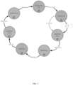
- FIG. 5 illustrates a state diagram of the PFC circuit 11 in accordance with the present disclosure.
- the PWM signal generator 1132 may be configured to provide a first PWM control signal for the power switch 112 and may further be configured to provide a second PWM control signal for the clamp switch 120.
- an on-time of the first PWM control signal may depend on a given minimum on-time t ON_LS_min , on a given maximum on-time t ON_LS_max , and on an instant of on-time expiration when the current 115, I through the series connection 111, 112 exceeds the peak current envelope 116, Î for the same. This corresponds to the peak-current control of the power switch 112.
- an on-time of the second PWM control signal may depend on a given on-time t ON_HS . This corresponds to an active clamping of the inductance 111, thereby supplying the energy stored in a leakage inductance (not shown) of the inductance 111 to the LED load 2, R 11 and improving a converter efficiency.
- a peak voltage across the power switch 112 during its turn-off events may be reduced significantly, resulting in a lower voltage rating of the power switch 112.
- the on-times of the first and second PWM control signals may be mutually exclusive in accordance with a dead-time depending on a given minimum dead-time t dead_min , and on an instant of dead-time expiration when a time derivative d dt of a drain-source voltage V ds of a last active switch of the power switch 112 and the clamp switch 120 becomes zero. More specifically, in states 43 to 45 the power switch 112 was last active, whereas in states 46 to 41 the clamp switch 120 was last active. Note that a dead time when the power switch 112 was last active may be different from a dead time when the clamp switch 120 was last active.
- FIG. 6 illustrates a various electrical quantities of the PFC circuit 11 in accordance with the present disclosure.
- FIG. 6 A top diagram of FIG. 6 shows a control variable 119, R of the control circuit 113 and a DC component 117, Î DC of the peak current envelope 116, Î vs. LED load 2, R 11 , whereas a bottom diagram of FIG. 6 depicts the regulated output voltage 114, V out and an output power 118, P of the PFC circuit 11 vs. LED load 2, R 11 .
- the output power 118, P V out 2 R 11 declines inversely proportional to the LED load 2, R 11 , as may be expected in connection with the regulated output voltage 114, V out .
- the control variable 119, R shows a similar decline vs. the LED load 2, R 11 .
- the DC component 117, Î DC depending on the control variable 119, R rises with increasing LED load 2, R 11 and approaches an asymptotic value. It may be established that the DC component 117, Î DC varies with / depends on LED load 2, R 11 , or alternatively on the output power 118, P.
- an increase in the output power 118, P therefore coincides with a decrease in the DC component 117, Î DC , and vice versa.
Landscapes
- Engineering & Computer Science (AREA)
- Power Engineering (AREA)
- Dc-Dc Converters (AREA)
- Rectifiers (AREA)
Abstract
Disclosed is a converter (1) for an LED load (2). The converter (1) comprises a power factor correction, PFC, circuit (11). The PFC circuit (11) comprises a series connection (111, 112) of an inductance (111) and a power switch (112); and a control circuit (113). The control circuit (113) is configured to regulate an output voltage (114, Vout) of the PFC circuit (11) in accordance with a current (115, I) through the series connection (111, 112) and a peak current envelope (116, Î) for the same; and to offset the peak current envelope (116, Î) by a direct current, DC, component (117, ÎDC ) that depends on an output power of the PFC circuit (11). This results in a low-THD peak-current control for the whole output power range of the converter (1).
Description
- The present disclosure relates to lighting technology, and in particular, to a converter for a light-emitting diode (LED) load, and a luminaire based thereon.
- Power factor correction (PFC) circuits attempt to maximize a power factor of a connected load by drawing from an alternating current (AC) power supply an AC current that corresponds in amplitude curve and phase to the supplied AC voltage, thereby minimizing a Total Harmonic Distortion (THD).
- Such PFC circuits typically make use of peak-current control, since an average-current control needs a more complicate current sensing.
- Due to parasitic effects in the components of a PFC circuit, it turns out that a peak-current control results in a non-zero voltage plateau across the EMI capacitor around the zero-crossings of the supplied AC voltage, which ultimately results in a higher THD.
- Integrated circuits (ICs) for analog peak-current control do not avoid or reduce said plateau, whereas ICs for digital peak-current control typically increase an on-time of a power switch of the PFC circuit close to the zero-crossings via calculations or table-based loop-up. A parameterization of such solutions is difficult because of their relatively complicated design, and for higher switching frequencies multiple look-up tables may be needed.
- It is an object to overcome the above-mentioned and other drawbacks. The objective is achieved by the embodiments as defined by the appended independent claims. Preferred embodiments are set forth in the dependent claims and in the following description and drawings.
- A first aspect of the present disclosure relates to a converter for an LED load. The converter comprises a power factor correction, PFC, circuit. The PFC circuit comprises a series connection of an inductance and a power switch; and a control circuit. The control circuit is configured to regulate an output voltage of the PFC circuit in accordance with a current through the series connection and a peak current envelope for the same; and to offset the peak current envelope by a direct current, DC, component that depends on an output power of the PFC circuit.
- The peak current envelope may depend on a control variable of the control circuit. The control variable may depend on a differential of the output voltage and its reference variable, and on a multiplicative fraction of a rectified input voltage of the PFC circuit.
- The DC component may depend on the control variable of the control circuit, a constant coefficient of the control variable, and a constant offset of the DC component.
- The constant coefficient and the constant offset may be derived from simulations or measurements at a minimum value and a maximum value of the output power of the PFC circuit.
- The control circuit may comprise a proportional integral, PI, controller, being configured to provide the control variable of the control circuit in dependence of the differential of the output voltage and its reference variable.
- The control circuit may comprise a pulse width modulation, PWM, signal generator, being configured to provide a first PWM control signal for the power switch in accordance with the control variable, the current through the series connection and the peak current envelope for the same.
- An on-time of the first PWM control signal may depend on a given minimum on-time, on a given maximum on-time, and on an instant of on-time expiration when the current through the series connection exceeds the peak current envelope for the same.
- The PFC circuit may comprise a Boost converter; and the first PWM control signal may be in accordance with one of: a discontinuous conduction mode, DCM, and a borderline conduction mode, BCM.
- The PFC circuit may comprise a Flyback converter.
- The Flyback converter may comprise a further series connection of a clamp switch and a clamp capacitance in parallel with the inductance.
- The PWM signal generator may further be configured to provide a second PWM control signal for the clamp switch.
- An on-time of the second PWM control signal may depend on a given on-time.
- The on-times of the first and second PWM control signals may be mutually exclusive in accordance with a dead-time depending on a given minimum dead-time, and on an instant of dead-time expiration when a time derivative of a drain-source voltage of a last active switch of the power switch and the clamp switch becomes zero.
- A second aspect of the present disclosure relates to a luminaire, comprising an LED load and a converter of the first aspect.
- If a simple peak-current control is used, adding a DC component to the sinusoidal peak-current envelope improves an AC current waveform close to zero-crossing, but if the DC component is constant, the THD at low output power is adverse.
- A DC component that depends on the output power of the PFC circuit provides a simple control scheme for good THD over a wide output power range.
- The DC component proposed herein comprises a constant coefficient and a constant offset wherein both constants are derived from simulations or measurements at a minimum value and a maximum value of the output power of the PFC circuit. Notably, the constants themselves are independent of the output voltage of the PFC stage but do capture the dependency of the DC component of the output voltage by a simple parameterization.
- The parameterized DC component avoids or at least reduces the non-zero voltage plateau across the EMI capacitor around the zero-crossings of the supplied AC voltage for the whole output power range, ultimately resulting in a low THD.
- In contrast to digital approaches which typically increase the on-time of the power switch of the PFC circuit close to the zero-crossings
to correct the discharge of the EMI capacitor, adding a DC component / offset that depends on the output power but involves constant values that are independent of the output power is very simple and robust and independent of a switching frequency of the PFC circuit. - In turn, the switching frequency may be increased and a size of passive components may be reduced.
- The technical effects and advantages described above equally apply to the converter and to the luminaire comprising the same.
- The above-described aspects and implementations will now be explained with reference to the accompanying drawings, in which the same or similar reference numerals designate the same or similar elements.
- The features of these aspects and implementations may be combined with each other unless specifically stated otherwise.
- The drawings are to be regarded as being schematic representations, and elements illustrated in the drawings are not necessarily shown to scale. Rather, the various elements are represented such that their function and general purpose become apparent to those skilled in the art.
- FIG. 1
- illustrates a luminaire in accordance with the present disclosure;
- FIG. 2
- illustrates a converter in accordance with the present disclosure;
- FIG. 3
- illustrates a PFC circuit in accordance with the present disclosure;
- FIG. 4
- illustrates a drive circuit for the
clamp switch 120; - FIG. 5
- illustrates a state diagram of the PFC circuit in accordance with the present disclosure; and
- FIG. 6
- illustrates a various electrical quantities of the PFC circuit in accordance with the present disclosure.
-
FIG. 1 illustrates aluminaire 3 in accordance with the present disclosure. - The
luminaire 3 comprises anLED load 2, R11 and a converter 1 for theLED load 2, R 11. - The
LED load 2, R11 may comprise one or more LEDs in series and/or in parallel, depending on the lighting scenario. -
FIG. 2 illustrates a converter 1 in accordance with the present disclosure. - The converter 1 comprises a PFC circuit/
stage 11 and may further comprise a DC-DC converter/stage 12. -
FIG. 3 illustrates aPFC circuit 11 in accordance with the present disclosure. - PFC may refer to a maximization of a power factor of a connected load by drawing from an AC power supply an AC current that corresponds in amplitude curve and phase to the supplied AC voltage, thereby minimizing a THD.
- A power factor of an AC circuit may refer to a ratio of a real power absorbed by a connected load to an apparent power flowing in the circuit.
- A THD may refer to a ratio of a sum of powers of all harmonic frequency components to a power of the fundamental frequency.
- In accordance with
FIG. 3 , thePFC circuit 11 comprises a Flyback converter. Alternatively, a Boost converter (not shown) being operated in accordance with modes of operation such as a discontinuous conduction mode (DCM) or a borderline conduction mode (BCM) may be deployed as well. - The
PFC circuit 11 comprises aseries connection inductance 111 and apower switch 112. - In accordance with
FIG. 3 , theinductance 111 may be modelled as a parallel circuit of a magnetizing inductance L2 and a primary inductance L4 of an ideal transformer, for example. - The
power switch 112 may in particular comprise a power semiconductor switch, such as a power metal-oxide-semiconductor field-effect transistor (MOSFET). - The
PFC circuit 11 further comprises acontrol circuit 113. - The
control circuit 113 is configured to regulate anoutput voltage 114, Vout of thePFC circuit 11 in accordance with a current 115, I through theseries connection current envelope 116, Î for the same. - In accordance with
FIG. 3 , theoutput voltage 114, Vout may be tapped off at theLED load 2, R 11 being connected to an output port of thePFC circuit 11, the current 115, I through theseries connection power switch 112, and the peakcurrent envelope 116, Î for the current 115, I may be provided by a ground-referenced resistive voltage divider R2, R3 in parallel to an EMI capacitor C4. - The
control circuit 113 may comprise a proportional integral (PI)controller 1131 and aPWM signal generator 1132. - PWM may refer to a continual on-off modulation of an electrical quantity, such as a voltage, by a switch, in accordance with a particular mode of operation of the superordinate circuit. For example, a PFC circuit may involve a PWM in accordance with modes of operation such as the DCM, the BCM or a continuous conduction mode (CCM).
- The
PWM signal generator 1132 may be configured to provide a first PWM control signal for thepower switch 112 in accordance with acontrol variable 119, R of thecontrol circuit 113, the current 115, I through theseries connection current envelope 116, Î for the same. - The
PI controller 1131 may be configured to provide thecontrol variable 119, R of thecontrol circuit 113 in dependence of a differential Vout - Vout_ref of theoutput voltage 114, Vout and its reference variable Vout_ref. - The peak
current envelope 116, Î = C · |Vbus | · R(Vout - Vout_ref ) may depend on thecontrol variable 119, R of thecontrol circuit 113 and on a multiplicative fraction C of a rectified input voltage C · |Vbus | of thePFC circuit 11. - In accordance with
FIG. 3 , the multiplicative fraction C may correspond to a given ratio
- The
control circuit 113 is further configured to offset the peakcurrent envelope 116, Î by aDC component 117, ÎDC that depends on an output power of thePFC circuit 11. - The
DC component 117, ÎDC = k · R(Vout - Vout_ref ) + d may depend on thecontrol variable 119, R of thecontrol circuit 113, a constant coefficient k of thecontrol variable 119, R, and a constant offset d of theDC component 117, ÎDC . - The constant coefficient k and the constant offset d may be derived from simulations or measurements at a minimum value and a maximum value of the output power of the
PFC circuit 11, thereby capturing the dependency of theDC component 117, ÎDC on the output power of thePFC circuit 11 over the whole output power range. - The Flyback converter may comprise a
further series connection clamp switch 120 and aclamp capacitance 121 in parallel with theinductance 111, thereby ending up with an active clamp Flyback (ACF) converter. - The
PWM signal generator 1132 may further be configured to provide a second PWM control signal for theclamp switch 120. - The floating electric reference potential of the
clamp switch 120 may require a so-called high-side drive circuit, such as the one illustrated inFIG. 4 being operable in a transforming manner. - More specifically,
FIG. 4 illustrates an exemplary implementation of adrive circuit 123 for theclamp switch 120 including anancillary transformer 131, 132, which may be connected to the PWM signal generator 1132 (seeFIG. 3 ) and configured to transform a drive current ISW2 in terms of its electric potential. - As indicated in
FIG. 4 , the (transformed) drive current ISW2 includes alternating trains of positive current pulses and negative current pulses. - The
clamp switch 120 is operable in accordance with the transformed drive current ISW2. To this end, thedrive circuit 123 may further comprise a circuitry for conditioning of the transformed drive current ISW2 into a control signal VSW2 of theclamp switch 120. - The conditioning circuitry is configured to convert each train of positive current pulses into a positive voltage pulse of the control signal VSW2, wherein a time duration of the positive voltage pulse corresponds to a time duration of the underlying train of positive current pulses.
- The conditioning circuitry is further configured to convert each train of negative current pulses into a zero line voltage of the control signal VSW2, wherein a time duration of the zero line voltage corresponds to a time duration of the underlying train of negative current pulses.
-
FIG. 5 illustrates a state diagram of thePFC circuit 11 in accordance with the present disclosure. - As previously explained, if the PFC circuit 1 comprises an ACF converter, the
PWM signal generator 1132 may be configured to provide a first PWM control signal for thepower switch 112 and may further be configured to provide a second PWM control signal for theclamp switch 120. - In accordance with
states 41 to 43 inFIG. 5 , an on-time of the first PWM control signal may depend on a given minimum on-time tON_LS_min, on a given maximum on-time tON_LS_max, and on an instant of on-time expiration when the current 115, I through theseries connection current envelope 116, Î for the same. This corresponds to the peak-current control of thepower switch 112. - In accordance with
states 45 to 46 inFIG. 5 , an on-time of the second PWM control signal may depend on a given on-time tON_HS. This corresponds to an active clamping of theinductance 111, thereby supplying the energy stored in a leakage inductance (not shown) of theinductance 111 to theLED load 2, R 11 and improving a converter efficiency. In addition, a peak voltage across thepower switch 112 during its turn-off events may be reduced significantly, resulting in a lower voltage rating of thepower switch 112. - In accordance with
states 43 to 45 and states 46 to 41 inFIG. 5 , the on-times of the first and second PWM control signals may be mutually exclusive in accordance with a dead-time depending on a given minimum dead-time tdead_min, and on an instant of dead-time expiration when a time derivative
power switch 112 and theclamp switch 120 becomes zero. More specifically, instates 43 to 45 thepower switch 112 was last active, whereas instates 46 to 41 theclamp switch 120 was last active. Note that a dead time when thepower switch 112 was last active may be different from a dead time when theclamp switch 120 was last active. -
FIG. 6 illustrates a various electrical quantities of thePFC circuit 11 in accordance with the present disclosure. - A top diagram of
FIG. 6 shows acontrol variable 119, R of thecontrol circuit 113 and aDC component 117, ÎDC of the peakcurrent envelope 116, Î vs.LED load 2, R11, whereas a bottom diagram ofFIG. 6 depicts theregulated output voltage 114, Vout and anoutput power 118, P of thePFC circuit 11 vs.LED load 2, R 11 . - As can be seen, the
output power 118,
LED load 2, R 11, as may be expected in connection with theregulated output voltage 114, Vout. - The
control variable 119, R shows a similar decline vs. theLED load 2, R 11. - The
DC component 117, ÎDC depending on thecontrol variable 119, R rises with increasingLED load 2, R 11 and approaches an asymptotic value. It may be established that theDC component 117, ÎDC varies with / depends onLED load 2, R11, or alternatively on theoutput power 118, P. - In accordance with
FIG. 6 , an increase in theoutput power 118, P therefore coincides with a decrease in theDC component 117, ÎDC, and vice versa.
Claims (14)
- A converter (1) for an LED load (2), comprising
a power factor correction, PFC, circuit (11), comprisinga series connection (111, 112) of an inductance (111) and a power switch (112); anda control circuit (113), being configured toregulate an output voltage (114, Vout ) of the PFC circuit (11) in accordance with a current (115, I) through the series connection (111, 112) and a peak current envelope (116, Î) for the same; andoffset the peak current envelope (116, Î) by a direct current, DC, component (117, ÎDC ) that depends on an output power of the PFC circuit (11). - The converter (1) of claim 1,
the peak current envelope (116, Î = C · |Vbus | · R(Vout - Vout_ref )) depending- on a control variable (119, R) of the control circuit (113), the control variable (119, R) depending on a differential (Vout - Vout_ref ) of the output voltage (114, Vout ) and its reference variable (Vout_ref ), and- on a multiplicative fraction of a rectified input voltage (C · |Vbus |) of the PFC circuit (11). - The converter (1) of claim 2,
the DC component (117, ÎDC = k · R(Vout - Vout_ref ) + d) depending- on the control variable (119, R) of the control circuit (113),- on a constant coefficient (k) of the control variable (119, R), and- on a constant offset (d) of the DC component (117, ÎDC ). - The converter (1) of claim 3,
the constant coefficient (k) and the constant offset (d) being derived from simulations or measurements at a minimum value and a maximum value of the output power of the PFC circuit (11). - The converter (1) of any one of the claims 2 to 4,
the control circuit (113) comprising a proportional integral, PI, controller (1131), being configured to provide the control variable (119, R) of the control circuit (113) in dependence of the differential (Vout - Vout_ref ) of the output voltage (114, Vout ) and its reference variable (Vout_ref ). - The converter (1) of any one of the claims 2 to 5,
the control circuit (113) comprising a pulse width modulation, PWM, signal generator (1132), being configured to provide a first PWM control signal for the power switch (112) in accordance with the control variable (119, R), the current (115, I) through the series connection (111, 112) and the peak current envelope (116, Î) for the same. - The converter (1) of claim 6,
an on-time of the first PWM control signal depending- on a given minimum on-time (tON_LS_min ),- on a given maximum on-time (tON_LS_max ), and- on an instant of on-time expiration when the current (115, I) through the series connection (111, 112) exceeds the peak current envelope (116, Î) for the same. - The converter (1) of claim 7,the PFC circuit (11) comprising a Boost converter; andthe first PWM control signal being in accordance with one of:- a discontinuous conduction mode, DCM, and- a borderline conduction mode, BCM.
- The converter (1) of claim 6 or claim 7,
the PFC circuit (11) comprising a Flyback converter. - The converter (1) of claim 9,
the Flyback converter comprising a further series connection (120, 121) of a clamp switch (120) and a clamp capacitance (121) in parallel with the inductance (111). - The converter (1) of claim 10,
the PWM signal generator (1132) further being configured to provide a second PWM control signal for the clamp switch (120). - The converter (1) of claim 10,
an on-time of the second PWM control signal depending- on a given on-time (tON_HS ). - The converter (1) of claim 1,
the on-times of the first and second PWM control signals being mutually exclusive in accordance with a dead-time depending- on a given minimum dead-time (tdead_min ), and- on an instant of dead-time expiration when a time derivative of a drain-source voltage of a last active switch of the power switch (112) and the clamp switch (120) becomes zero. - A luminaire (3), comprising
an LED load (2); and
a converter (1) of any of the preceding claims for the LED load (2).
Priority Applications (3)
| Application Number | Priority Date | Filing Date | Title |
|---|---|---|---|
| EP23170234.1A EP4456671A1 (en) | 2023-04-27 | 2023-04-27 | Converter for a light-emitting diode load |
| EP24722030.4A EP4666813A1 (en) | 2023-04-27 | 2024-04-26 | Converter for a light-emitting diode load |
| PCT/EP2024/061494 WO2024223798A1 (en) | 2023-04-27 | 2024-04-26 | Converter for a light-emitting diode load |
Applications Claiming Priority (1)
| Application Number | Priority Date | Filing Date | Title |
|---|---|---|---|
| EP23170234.1A EP4456671A1 (en) | 2023-04-27 | 2023-04-27 | Converter for a light-emitting diode load |
Publications (1)
| Publication Number | Publication Date |
|---|---|
| EP4456671A1 true EP4456671A1 (en) | 2024-10-30 |
Family
ID=86272297
Family Applications (2)
| Application Number | Title | Priority Date | Filing Date |
|---|---|---|---|
| EP23170234.1A Withdrawn EP4456671A1 (en) | 2023-04-27 | 2023-04-27 | Converter for a light-emitting diode load |
| EP24722030.4A Pending EP4666813A1 (en) | 2023-04-27 | 2024-04-26 | Converter for a light-emitting diode load |
Family Applications After (1)
| Application Number | Title | Priority Date | Filing Date |
|---|---|---|---|
| EP24722030.4A Pending EP4666813A1 (en) | 2023-04-27 | 2024-04-26 | Converter for a light-emitting diode load |
Country Status (2)
| Country | Link |
|---|---|
| EP (2) | EP4456671A1 (en) |
| WO (1) | WO2024223798A1 (en) |
Citations (5)
| Publication number | Priority date | Publication date | Assignee | Title |
|---|---|---|---|---|
| US4437146A (en) * | 1982-08-09 | 1984-03-13 | Pacific Electro Dynamics, Inc. | Boost power supply having power factor correction circuit |
| US20120176101A1 (en) * | 2011-01-07 | 2012-07-12 | Tdk-Lambda Uk Limited | Power Factor Correction Device |
| WO2014009773A1 (en) * | 2012-07-11 | 2014-01-16 | Roal Electronics S.P.A. | Control circuit for reducing of total harmonic distortion (thd) in the power supply to an electric load |
| US9621029B2 (en) * | 2015-03-18 | 2017-04-11 | Stmicroelectronics S.R.L. | Method and device for high-power-factor flyback converter |
| EP3736959A1 (en) * | 2019-05-09 | 2020-11-11 | Tridonic GmbH & Co. KG | Resonant hb converter |
Family Cites Families (2)
| Publication number | Priority date | Publication date | Assignee | Title |
|---|---|---|---|---|
| KR101357727B1 (en) * | 2011-09-08 | 2014-02-06 | 주식회사 동부하이텍 | Isolation-type flyback converter for light emitting diode driver |
| US20210399643A1 (en) * | 2020-06-17 | 2021-12-23 | Apple Inc. | Active Clamp Resonant Flyback Converter with Integrated Boost Stage |
-
2023
- 2023-04-27 EP EP23170234.1A patent/EP4456671A1/en not_active Withdrawn
-
2024
- 2024-04-26 EP EP24722030.4A patent/EP4666813A1/en active Pending
- 2024-04-26 WO PCT/EP2024/061494 patent/WO2024223798A1/en not_active Ceased
Patent Citations (5)
| Publication number | Priority date | Publication date | Assignee | Title |
|---|---|---|---|---|
| US4437146A (en) * | 1982-08-09 | 1984-03-13 | Pacific Electro Dynamics, Inc. | Boost power supply having power factor correction circuit |
| US20120176101A1 (en) * | 2011-01-07 | 2012-07-12 | Tdk-Lambda Uk Limited | Power Factor Correction Device |
| WO2014009773A1 (en) * | 2012-07-11 | 2014-01-16 | Roal Electronics S.P.A. | Control circuit for reducing of total harmonic distortion (thd) in the power supply to an electric load |
| US9621029B2 (en) * | 2015-03-18 | 2017-04-11 | Stmicroelectronics S.R.L. | Method and device for high-power-factor flyback converter |
| EP3736959A1 (en) * | 2019-05-09 | 2020-11-11 | Tridonic GmbH & Co. KG | Resonant hb converter |
Non-Patent Citations (1)
| Title |
|---|
| SEBASTIAN J ET AL: "Improving power factor correction in distributed power supply systems using PWM and ZCS-QR SEPIC topologies", PROCEEDINGS OF THE ANNUAL POWER ELECTRONICS SPECIALISTS CONFERENCE. MASSACHUSETTS, 25 - 27 JUNE, 1991; [PROCEEDINGS OF THE ANNUAL POWER ELECTRONICS SPECIALISTS CONFERENCE], NEW YORK, IEEE, US, vol. CONF. 22, 24 June 1991 (1991-06-24), pages 780 - 791, XP010048400, ISBN: 978-0-7803-0090-3, DOI: 10.1109/PESC.1991.162764 * |
Also Published As
| Publication number | Publication date |
|---|---|
| WO2024223798A1 (en) | 2024-10-31 |
| EP4666813A1 (en) | 2025-12-24 |
Similar Documents
| Publication | Publication Date | Title |
|---|---|---|
| US10015849B2 (en) | Ripple cancellation converter with high power factor | |
| EP3437178B1 (en) | An ac/dc pfc converter using a half bridge resonant converter, and corresponding conversion method | |
| CN108539984B (en) | PFWM Control System of Switching Power Supply Circuit | |
| US8493757B2 (en) | AC/DC converter with a PFC and a DC/DC converter | |
| CN101282079B (en) | System and method for power controller | |
| US8503204B2 (en) | Power converter circuit | |
| US20100259240A1 (en) | Bridgeless PFC converter | |
| US20180004240A1 (en) | Device and method for quasi-resonant-mode voltage control of a switching converter | |
| US10256712B2 (en) | Current ripple sensing controller for a single-stage LED driver | |
| EP2781011A1 (en) | Led power source with over-voltage protection | |
| US20100259957A1 (en) | Bridgeless pfc circuit for critical continuous current mode and controlling method thereof | |
| EP3895298A1 (en) | Ac-dc power converter with power factor correction | |
| CN1293885A (en) | Electronic lamp ballast with power fractor correction | |
| Luewisuthichat et al. | Analysis and implement DC-DC integrated boost-flyback converter with LED street light stand-by application | |
| US20150181675A1 (en) | Power factor correction circuit, operating device for a light-emitting means and method for controlling a power factor correction circuit | |
| US10581321B1 (en) | Flyback converter with multiplier signal control circuit and method | |
| US6819575B1 (en) | AC/DC switch mode power supply with power factor correction using direct energy transfer concept | |
| KR101609726B1 (en) | Control circuit of switching rectifier with high power factor | |
| US20140002035A1 (en) | Common-core power factor correction resonant converter | |
| KR100420964B1 (en) | Single-stage converter compensating power factor | |
| CN106413202A (en) | Primary side control LED drive circuit based on SEPIC and Flyback circuit | |
| CN113872455B (en) | Boost converter for electric load power supply device, power supply device and method for boosting input voltage in electric load power supply device | |
| EP4666813A1 (en) | Converter for a light-emitting diode load | |
| KR20190019547A (en) | Simple control circuit of switching rectifier with high power factor | |
| Farcas et al. | A novel topology based on forward converter with passive power factor correction |
Legal Events
| Date | Code | Title | Description |
|---|---|---|---|
| PUAI | Public reference made under article 153(3) epc to a published international application that has entered the european phase |
Free format text: ORIGINAL CODE: 0009012 |
|
| STAA | Information on the status of an ep patent application or granted ep patent |
Free format text: STATUS: THE APPLICATION HAS BEEN PUBLISHED |
|
| AK | Designated contracting states |
Kind code of ref document: A1 Designated state(s): AL AT BE BG CH CY CZ DE DK EE ES FI FR GB GR HR HU IE IS IT LI LT LU LV MC ME MK MT NL NO PL PT RO RS SE SI SK SM TR |
|
| STAA | Information on the status of an ep patent application or granted ep patent |
Free format text: STATUS: THE APPLICATION IS DEEMED TO BE WITHDRAWN |
|
| 18D | Application deemed to be withdrawn |
Effective date: 20250501 |