EP4456421A1 - Method and apparatus for interference reduction in optical sensing receivers - Google Patents
Method and apparatus for interference reduction in optical sensing receivers Download PDFInfo
- Publication number
- EP4456421A1 EP4456421A1 EP24170244.8A EP24170244A EP4456421A1 EP 4456421 A1 EP4456421 A1 EP 4456421A1 EP 24170244 A EP24170244 A EP 24170244A EP 4456421 A1 EP4456421 A1 EP 4456421A1
- Authority
- EP
- European Patent Office
- Prior art keywords
- circuit
- voltage
- photodetector
- coupled
- current
- Prior art date
- Legal status (The legal status is an assumption and is not a legal conclusion. Google has not performed a legal analysis and makes no representation as to the accuracy of the status listed.)
- Pending
Links
Images


Classifications
-
- G—PHYSICS
- G01—MEASURING; TESTING
- G01J—MEASUREMENT OF INTENSITY, VELOCITY, SPECTRAL CONTENT, POLARISATION, PHASE OR PULSE CHARACTERISTICS OF INFRARED, VISIBLE OR ULTRAVIOLET LIGHT; COLORIMETRY; RADIATION PYROMETRY
- G01J1/00—Photometry, e.g. photographic exposure meter
- G01J1/42—Photometry, e.g. photographic exposure meter using electric radiation detectors
- G01J1/44—Electric circuits
-
- H—ELECTRICITY
- H03—ELECTRONIC CIRCUITRY
- H03F—AMPLIFIERS
- H03F3/00—Amplifiers with only discharge tubes or only semiconductor devices as amplifying elements
- H03F3/45—Differential amplifiers
- H03F3/45071—Differential amplifiers with semiconductor devices only
- H03F3/45076—Differential amplifiers with semiconductor devices only characterised by the way of implementation of the active amplifying circuit in the differential amplifier
- H03F3/45475—Differential amplifiers with semiconductor devices only characterised by the way of implementation of the active amplifying circuit in the differential amplifier using IC blocks as the active amplifying circuit
-
- H—ELECTRICITY
- H04—ELECTRIC COMMUNICATION TECHNIQUE
- H04B—TRANSMISSION
- H04B10/00—Transmission systems employing electromagnetic waves other than radio-waves, e.g. infrared, visible or ultraviolet light, or employing corpuscular radiation, e.g. quantum communication
- H04B10/60—Receivers
- H04B10/66—Non-coherent receivers, e.g. using direct detection
- H04B10/69—Electrical arrangements in the receiver
- H04B10/693—Arrangements for optimizing the preamplifier in the receiver
-
- G—PHYSICS
- G01—MEASURING; TESTING
- G01J—MEASUREMENT OF INTENSITY, VELOCITY, SPECTRAL CONTENT, POLARISATION, PHASE OR PULSE CHARACTERISTICS OF INFRARED, VISIBLE OR ULTRAVIOLET LIGHT; COLORIMETRY; RADIATION PYROMETRY
- G01J1/00—Photometry, e.g. photographic exposure meter
- G01J1/42—Photometry, e.g. photographic exposure meter using electric radiation detectors
- G01J1/44—Electric circuits
- G01J1/46—Electric circuits using a capacitor
-
- H—ELECTRICITY
- H03—ELECTRONIC CIRCUITRY
- H03F—AMPLIFIERS
- H03F3/00—Amplifiers with only discharge tubes or only semiconductor devices as amplifying elements
- H03F3/04—Amplifiers with only discharge tubes or only semiconductor devices as amplifying elements with semiconductor devices only
- H03F3/08—Amplifiers with only discharge tubes or only semiconductor devices as amplifying elements with semiconductor devices only controlled by light
- H03F3/087—Amplifiers with only discharge tubes or only semiconductor devices as amplifying elements with semiconductor devices only controlled by light with IC amplifier blocks
-
- H—ELECTRICITY
- H03—ELECTRONIC CIRCUITRY
- H03F—AMPLIFIERS
- H03F3/00—Amplifiers with only discharge tubes or only semiconductor devices as amplifying elements
- H03F3/45—Differential amplifiers
- H03F3/45071—Differential amplifiers with semiconductor devices only
- H03F3/45479—Differential amplifiers with semiconductor devices only characterised by the way of common mode signal rejection
- H03F3/45928—Differential amplifiers with semiconductor devices only characterised by the way of common mode signal rejection using IC blocks as the active amplifying circuit
- H03F3/4595—Differential amplifiers with semiconductor devices only characterised by the way of common mode signal rejection using IC blocks as the active amplifying circuit by using feedforward means
- H03F3/45955—Measuring at the input circuit of the differential amplifier
- H03F3/45959—Controlling the input circuit of the differential amplifier
-
- H—ELECTRICITY
- H03—ELECTRONIC CIRCUITRY
- H03F—AMPLIFIERS
- H03F3/00—Amplifiers with only discharge tubes or only semiconductor devices as amplifying elements
- H03F3/45—Differential amplifiers
- H03F3/45071—Differential amplifiers with semiconductor devices only
- H03F3/45479—Differential amplifiers with semiconductor devices only characterised by the way of common mode signal rejection
- H03F3/45928—Differential amplifiers with semiconductor devices only characterised by the way of common mode signal rejection using IC blocks as the active amplifying circuit
- H03F3/45968—Differential amplifiers with semiconductor devices only characterised by the way of common mode signal rejection using IC blocks as the active amplifying circuit by offset reduction
- H03F3/45973—Differential amplifiers with semiconductor devices only characterised by the way of common mode signal rejection using IC blocks as the active amplifying circuit by offset reduction by using a feedback circuit
- H03F3/45977—Differential amplifiers with semiconductor devices only characterised by the way of common mode signal rejection using IC blocks as the active amplifying circuit by offset reduction by using a feedback circuit using switching means, e.g. sample and hold
-
- H—ELECTRICITY
- H03—ELECTRONIC CIRCUITRY
- H03H—IMPEDANCE NETWORKS, e.g. RESONANT CIRCUITS; RESONATORS
- H03H11/00—Networks using active elements
- H03H11/02—Multiple-port networks
- H03H11/04—Frequency selective two-port networks
-
- H—ELECTRICITY
- H04—ELECTRIC COMMUNICATION TECHNIQUE
- H04B—TRANSMISSION
- H04B10/00—Transmission systems employing electromagnetic waves other than radio-waves, e.g. infrared, visible or ultraviolet light, or employing corpuscular radiation, e.g. quantum communication
- H04B10/60—Receivers
- H04B10/66—Non-coherent receivers, e.g. using direct detection
- H04B10/69—Electrical arrangements in the receiver
- H04B10/697—Arrangements for reducing noise and distortion
-
- G—PHYSICS
- G01—MEASURING; TESTING
- G01J—MEASUREMENT OF INTENSITY, VELOCITY, SPECTRAL CONTENT, POLARISATION, PHASE OR PULSE CHARACTERISTICS OF INFRARED, VISIBLE OR ULTRAVIOLET LIGHT; COLORIMETRY; RADIATION PYROMETRY
- G01J1/00—Photometry, e.g. photographic exposure meter
- G01J1/42—Photometry, e.g. photographic exposure meter using electric radiation detectors
- G01J1/44—Electric circuits
- G01J2001/444—Compensating; Calibrating, e.g. dark current, temperature drift, noise reduction or baseline correction; Adjusting
-
- H—ELECTRICITY
- H03—ELECTRONIC CIRCUITRY
- H03F—AMPLIFIERS
- H03F2200/00—Indexing scheme relating to amplifiers
- H03F2200/114—Indexing scheme relating to amplifiers the amplifier comprising means for electro-magnetic interference [EMI] protection
-
- H—ELECTRICITY
- H03—ELECTRONIC CIRCUITRY
- H03F—AMPLIFIERS
- H03F2200/00—Indexing scheme relating to amplifiers
- H03F2200/144—Indexing scheme relating to amplifiers the feedback circuit of the amplifier stage comprising a passive resistor and passive capacitor
-
- H—ELECTRICITY
- H03—ELECTRONIC CIRCUITRY
- H03F—AMPLIFIERS
- H03F2200/00—Indexing scheme relating to amplifiers
- H03F2200/261—Amplifier which being suitable for instrumentation applications
-
- H—ELECTRICITY
- H03—ELECTRONIC CIRCUITRY
- H03F—AMPLIFIERS
- H03F2200/00—Indexing scheme relating to amplifiers
- H03F2200/267—A capacitor based passive circuit, e.g. filter, being used in an amplifying circuit
-
- H—ELECTRICITY
- H03—ELECTRONIC CIRCUITRY
- H03F—AMPLIFIERS
- H03F2200/00—Indexing scheme relating to amplifiers
- H03F2200/27—A biasing circuit node being switched in an amplifier circuit
-
- H—ELECTRICITY
- H03—ELECTRONIC CIRCUITRY
- H03F—AMPLIFIERS
- H03F2203/00—Indexing scheme relating to amplifiers with only discharge tubes or only semiconductor devices as amplifying elements covered by H03F3/00
- H03F2203/45—Indexing scheme relating to differential amplifiers
- H03F2203/45138—Two or more differential amplifiers in IC-block form are combined, e.g. measuring amplifiers
-
- H—ELECTRICITY
- H03—ELECTRONIC CIRCUITRY
- H03F—AMPLIFIERS
- H03F2203/00—Indexing scheme relating to amplifiers with only discharge tubes or only semiconductor devices as amplifying elements covered by H03F3/00
- H03F2203/45—Indexing scheme relating to differential amplifiers
- H03F2203/45512—Indexing scheme relating to differential amplifiers the FBC comprising one or more capacitors, not being switched capacitors, and being coupled between the LC and the IC
-
- H—ELECTRICITY
- H03—ELECTRONIC CIRCUITRY
- H03F—AMPLIFIERS
- H03F2203/00—Indexing scheme relating to amplifiers with only discharge tubes or only semiconductor devices as amplifying elements covered by H03F3/00
- H03F2203/45—Indexing scheme relating to differential amplifiers
- H03F2203/45528—Indexing scheme relating to differential amplifiers the FBC comprising one or more passive resistors and being coupled between the LC and the IC
-
- H—ELECTRICITY
- H03—ELECTRONIC CIRCUITRY
- H03F—AMPLIFIERS
- H03F2203/00—Indexing scheme relating to amplifiers with only discharge tubes or only semiconductor devices as amplifying elements covered by H03F3/00
- H03F2203/45—Indexing scheme relating to differential amplifiers
- H03F2203/45536—Indexing scheme relating to differential amplifiers the FBC comprising a switch and being coupled between the LC and the IC
Definitions
- the present description relates generally to receivers for optical sensing, including optical detectors, and in particular, to reduction of interference including radio frequency (RF) interference.
- RF radio frequency
- Optical sensing devices that include optical detectors are used for sensing optical signals.
- Optical signals may be weak and require amplification up to a hundred times or more by amplifier circuits.
- Electronic circuits including optical sensing devices are prone to electromagnetic interference.
- interference signals caused by electromagnetic interference may be added to the optical signal and amplified, up to a hundred times or more, by the amplifier circuits and contaminate the optical signals. Therefore, it is highly desirable to minimize the interference signal before being added to the optical signals and before the optical signal is amplified.
- an apparatus comprising:
- the first circuit comprises a third voltage source configured to generate the common mode voltage.
- the first circuit comprises: an operational-amplifier (Op-Amp), wherein an inverting node of the Op-Amp is coupled to a first node between first and second capacitors of the first circuit, an output node of the Op-Amp is coupled to a second node between third and fourth capacitors of the first circuit, and the third voltage source is coupled between a non-inverting node of the Op-Amp and a ground to provide the common mode voltage to the non-inverting node of the Op-Amp.
- Op-Amp operational-amplifier
- the apparatus further comprises: a third circuit that comprises a low noise amplifier is coupled to the second circuit and is configured to amplify the current of the photodetector, received from the photodetector via the first circuit and the second circuit and provide an output voltage proportional to the current of the photodetector.
- a third circuit that comprises a low noise amplifier is coupled to the second circuit and is configured to amplify the current of the photodetector, received from the photodetector via the first circuit and the second circuit and provide an output voltage proportional to the current of the photodetector.
- the first, second, and third circuits provide differential signal paths.
- the second circuit is configured to provide the reverse-bias voltage, via the first circuit to the photodetector, and wherein the second circuit is configured to receive the current of the photodetector via the first circuit.
- voltages at the cathode and the anode of the photodetector are set at V o + 1/2V RB and V o - 1/2V RB respectively.
- an apparatus comprising:
- the second circuit is configured to receive the current from the first circuit and to provide the current
- the apparatus further comprising: a third circuit coupled to the second circuit and configured to receive the current, amplify the current, and provide an output voltage proportional to the current.
- the first, second, and third circuits provide fully differential signal paths.
- the apparatus further comprises: a photodetector coupled to the first port, wherein the first bias voltage plus the common mode voltage and the second bias voltage plus the common mode voltage are applied to a cathode and an anode of the photodetector to reverse-bias the photodetector by a sum of magnitudes of the first and second bias voltages (V RB ).
- the first bias voltage plus the common mode voltage is presented as V o + 1/2V RB that is applied to the cathode of the photodetector, and wherein the second bias voltage plus the common mode voltage is presented as V o - 1/2V RB that is applied to the cathode of the photodetector.
- the photodetector is reverse-biased by the sum of the magnitudes of the first and second bias voltages.
- the first circuit is configured to filter an electromagnetic interference, received by the first and second nodes of the first port, and prevent the electromagnetic interference, outside a frequency band of the current, from reaching the third circuit.
- an apparatus comprising:
- the apparatus further comprises: a fourth circuit coupled to the third circuit and configured to amplify a current of the photodetector, received via the second circuit and the third circuit, and provide an output voltage proportional to the current of the photodetector.
- the second circuit is configured to filter an electromagnetic interference, received by the first circuit, and prevent the electromagnetic interference from reaching the fourth circuit.
- the third circuit further comprises:
- the first and the second variable resistors are implemented by metal oxide semiconductor field effect transistors in weak inversion region to increase resistances of the first and the second variable resistors and to reduce thermal noise.
- a circuit for detecting optical signals may have closed loops and, thus, electromagnetic interference, e.g., radio frequency (RF) electromagnetic (EM) interference, e.g., electromagnetic signals induced by power lines and devices using alternating current, in the environment may generate currents and voltages in the closed loops of the circuit and may impact the detected signals.
- electromagnetic interference e.g., radio frequency (RF) electromagnetic (EM) interference
- RF radio frequency
- EM electromagnetic
- the detected optical signals produce low currents and voltages that require considerable amplification of hundred times or more to increase the detected signal to a voltage or current level that may be digitized and then processed. Because the electromagnetic interference is added to the detected signal before amplification, the amplification may also amplify the electromagnetic interference the same way that the detected optical signal is amplified.
- the circuits and apparatuses introduced below provide fully differential architectures for signal paths and have a very good interference rejection because of the symmetric structure.
- the interference affects both signal paths (positive and negative) nearly the same, so when the negative signal is subtracted from the positive signal, the interference on both signals cancels each other.
- the fully differential signal paths may cause the common-mode interference (CMI) to be subtracted between positive and negative output nodes and, thus, the CMI is rejected and RF electromagnetic (EM) interference and electrostatic discharge (ESD) effects are reduced.
- CMI common-mode interference
- EM electromagnetic
- ESD electrostatic discharge
- the circuit for detecting optical signals may reverse-bias a photodetector of the circuit for detecting optical signals and also may provide a common mode voltage, e.g., an offset voltage, to increase the dynamic range and prevent non-linearity, e.g., clipping from top or bottom.
- a common mode voltage e.g., an offset voltage
- the fully differential signal paths opens the possibility of increasing the common mode voltage to about half the supply rails. Higher common mode voltages reduce the non-linearity produced by ESD protection circuit and EMI due to balance swing, e.g., caused by reverse-biased diodes that are used for ESD protection.
- the optical signal is a periodic signal and the detected signal is a periodic voltage.
- the common mode voltage may be adjusted based on induced currents such that the detected current of the photodetector and the detected output voltage are not clipped from top or bottom.
- the circuits, devices, and systems introduced below that provide a differential architecture e.g., a fully differential architecture, reduces the input referred current detection error, induced by the CMI, to more than two orders of magnitude lower compared to circuits that do not have the fully differential architecture.
- the EMI impinging on the ESD diodes may be partially rectified by the ESD diodes out of the detector circuit 202 and partially remain and generate a current in the detector circuit 202 that is not from photodetector, causing error in the apparatus 300.
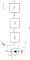
- FIG. 1 illustrates an apparatus for detecting and processing optical signals.
- An apparatus 100 of FIG. 1 shows a circuit 130, e.g., a circuit for detecting optical signals, which includes a photodetector 115 coupled between a voltage node 111 and a ground 114. As shown, an anode 106 of the photodetector 115 is coupled to the ground 114 and a cathode 108 of the photodetector 115 is coupled to the voltage node 111.
- a voltage V1 of the voltage node 111 is forced, e.g., induced, by the amplifier unit 102 and, thus, the photodetector 115 is reverse-biased by the voltage V1.
- the photodetector 115 is a diode that is reverse-biased and an optical signal 112, e.g., light rays, impinge on a depletion region (not shown) of the photodetector 115 to generate charge carriers proportional to an intensity of the light rays.
- the charged carriers are determined to be proportional to the intensity of the light rays and by increasing the intensity of the light rays by n times, where n is 2, 3, ..., the number of charged carriers is increased by n times.
- the generated charge carriers produce a current 120, e.g., an input signal, by the photodetector 115.
- the voltage V1 is between about 0 volts and 10 volts. In some embodiments, in a reverse-biased diode a voltage coupled to the cathode of the diode is higher than the voltage coupled to an anode of the diode. In some embodiments, the photodetector 115 is a diode that is reverse-biased.
- the apparatus 100 also includes an amplifier unit 102, a data acquisition unit, e.g., a DA unit 104, and a digital signal processing unit, e.g., a DSP unit 107.
- the current 120 or a voltage generated by the current 120 and proportional to the current 120 is amplified by the amplifier unit 102.
- the amplifier unit 102 amplifies the input signal several folds, e.g., a hundred times or more, to produce an output signal 122, e.g., a voltage, which is used by the DA unit 104.
- an EM interference e.g., EMI 110
- the EMI 110 may induce an interference current in the circuit 130 that is amplified along with the current 120 and is similarly added, as an interference signal, to the output signal of the amplifier unit 102 and, thus, the output signal 122 includes the interference signal.
- the output signal 122 of the amplifier unit 102 is received by the DA unit 104, as an input signal, to produce an output signal 124 of the DA unit 104.
- the DA unit 104 digitizes, by an analog to digital converter (not shown), the input signal and, thus, the output signal 124 is a digitized form of the output signal 122.
- the output signal 124 is then fed into the DSP unit 107 for processing and to generate an output signal 125.
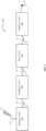
- FIG. 2 illustrates an apparatus for detecting optical signals, according to various aspects of the subject technology.
- an apparatus 200 of FIG. 2 shows is a combination of the circuit 130 and the amplifier unit 102 of FIG. 1 .
- the apparatus 200 includes a detector circuit 202 that includes the photodetector 115.
- the apparatus 200 also includes a feedback circuit 204, a bias circuit 206, and an amplifier circuit 208 that generates an output, e.g., an output voltage 360.
- the detector circuit 202 is coupled to the feedback circuit 204 through an interface 392.
- the feedback circuit 204 is coupled to the bias circuit 206 through an interface 394 and the bias circuit 206 is coupled the amplifier circuit 208 through an interface 396.
- the interfaces 392, 394, and 396 are used to coupled voltages and transfer current, at either direction, between the circuits at both sides of the interfaces 392, 394, and 396.
- the detector circuit 202, the feedback circuit 204, the bias circuit 206, the amplifier circuit 208, and the interfaces 392, 394, and 396 are described in more details below with respect to FIGS. 3A , 3B , and 3C .
- FIG. 2 also shows that the EMI 110 may affect the detector circuit 202 and may generate an EMI current, e.g., a current 215, in the detector circuit 202.
- the feedback circuit 204 is used to filter the EMI and prevents the EMI, e.g., the EMI outside the frequency band of the optical signal 112, from reaching the amplifier circuit 208 coupled to the bias circuit 206.
- the amplifier circuit 208 receives a current 363 via the feedback circuit 204 and the bias circuit 206.
- the resistors 316, 318, 336, and 338 have large resistance, e.g., more than one mega ohm and also the capacitors 322, 324, 332, and 334 are charged such that a sum of the currents through the resistors 316, 318, 336, and 338, and the currents through the capacitors 322, 324, 332, and 334 is negligible.
- the current 363 is almost the same as, e.g., within one percent difference of, a photodetector current 365.
- the amplifier circuit 208 amplifies the photodetector current 365 to provide the output voltage 360 that is proportional to the photodetector current 365.
- the currents through the resistors 316, 318, 336, and 338 is not negligible and adds a current bias is added to the photodetector current 365 and the current 363 is the photodetector current 365 plus a current bias.
- an output voltage 360 may be provided that is proportional to the photodetector current 365 plus a voltage bias such that the voltage bias may limit a dynamic range of the output voltage 360.
- the circuit-A by receiving a voltage at an interface coupled between two circuits, e.g., between circuit-A and circuit-B, the circuit-A provides, e.g., delivers, the voltage at the interface and the circuit-B receives the voltage at the interface.
- the interface is an output port of the circuit-A and also is an input port of the circuit-B.
- the output port of the circuit-A and the input port of the circuit-B are coupled through two nodes, e.g., node-1 and node-2.
- the circuit-A by receiving a current at the interface coupled between circuit-A and circuit-B, the circuit-A provides, e.g., delivers, the current at the node-1 of the interface and the circuit-B receives the current at the node-1 of the interface.
- FIGS. 3A , 3B , and 3C illustrate apparatuses for detecting optical signals and a circuit for reverse-biasing a photodetector, according to various aspects of the subject technology.
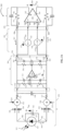
- FIG.3A shows the apparatus 300 for detecting optical signals 112 that impinge on the photodetector 115.
- the optical signal are optical pulses that are detected by the photodetector 115.
- the photodetector 115 is reverse-biased and, thus, a voltage between both ends of the photodetector 115, which is between a cathode 308 and an anode 306 of the photodetector 115, is a positive voltage.
- a voltage 366 e.g., a reverse-bias voltage V PD of the photodetector 115 is between about 0 volts and about 10 volts.
- the reverse-bias voltage V PD is applied in a symmetrical form such that half of the reverse-bias voltage, which is 1/2V PD is applied to the cathode 308 and -1/2V PD is applied to the anode 306.
- a capacitor 315 is coupled in parallel with the photodetector 115.
- a photodetector current 365 is generated by the photodetector 115 in the detector circuit 202, e.g., a first circuit.
- the capacitor 315 is used to cause a short-circuit parallel to the photodetector 115 for the current and/or voltage fluctuations, e.g., high frequency fluctuations, and prevent the fluctuation to impact the photodetector 115.
- ground bouncing interference to the photodetector 115 is absorbed by the capacitor 315 and the fully differential structure of the apparatus 300 is maintained.
- the detector circuit 202 is further coupled to a first group of ESD diodes D1 and D2 and to a second group of ESD diodes D3 and D4.
- the diode D1 is coupled and reverse-biased between the cathode 308 and the voltage node 116, which has a positive voltage between about 2 volts and 5 volts above the voltage of the cathode 308.
- the diode D2 is coupled and reverse-biased between the cathode 308 and the ground 114.
- the diodes D1 and D2 are reverse-biased diodes that are used for preventing a damage to the apparatus 300 because of the electrostatic discharge (ESD).
- the diodes D1 and D2 transfer at least a part of the ESD, out of the detector circuit 202.
- the diode D3 is coupled and reverse-biased between the anode 306 and a voltage node 117, which has a positive voltage between about 2 volts and 5 volts above the voltage of the anode 306.
- the diode D4 is coupled and reverse-biased between the anode 306 and the ground 114.
- the reverse-biased diodes D1 and D2 are coupled to the detector circuit 202 and adjacent to the cathode 308, and also reverse- biased diodes D3 and D4 are coupled to the detector circuit 202 and adjacent to the anode 306 and are used for preventing a damage to circuit components of the apparatus 300 due to electrostatic discharge (ESD) and transferring the ESD, e.g., at least part of the ESD, out of the detector circuit 202.
- ESD electrostatic discharge
- the EMI induced on the detector circuit may be rectified by the ESD diodes and because of the non-linearity of the ESD diodes may cause a current in the detector circuit 202, which is not from photodetector, causing error in the apparatus 300.
- the symmetrical configuration of the first and second groups of diodes helps balance the non-linearity on inverting node 326 and non-inverting node 328 of an operational-amplifier, Op-Amp 320, of the feedback circuit 204.
- the detector circuit 202 may be affected by the EMI from a power line, a neighboring device or circuit, and as shown in FIG. 1 , the EMI 110 may generate an additional current, the current 215 in the detector circuit 202 such that the current 215 is added to the photodetector current 365 of the photodetector 115.
- the current 215 is induced in the detector circuit 202, because the apparatus 300 provides fully differential signal paths, FIG. 3A shows that the addition of current 215, which is induced may conceptually be represented by the addition modules 302 and 304.
- the current 215 is applied as common mode to the apparatus 300 and is rejected, e.g., removed, by the fully differential structure of the apparatus 300.
- the current 215 includes the current caused by the non-linearity of the ESD diodes as described before.
- the first group of ESD diodes are physically close to about half of the source of the ESD and the second group of ESD diodes are physically close to another half of the source of the ESD.
- a combination of the feedback circuit 204, the bias circuit 206, and the amplifier circuit 208 provides the fully differential signal paths.
- the detector circuit 202 is connected to feedback circuit 204 through the interface 392 at an output of the detector circuit 202 and an input of the feedback circuit 204, which provides the common mode voltage for the reverse-biased photodetector 115.
- the interface 392 includes the two nodes 252 and 254, e.g., connection nodes, and voltages or currents are shared or transferred through the two nodes 252 and 254.
- the feedback circuit 204 includes a first RC circuit that includes a resistor 316, e.g., a first resistor, and a resistor 318, e.g., a second resistor coupled, in series, coupled to the interface 392 between the nodes 252 and 254.
- the first RC circuit further includes a capacitor 322, e.g., a first capacitor, and a capacitor 324, e.g., a second capacitor coupled to the interface 392 between the nodes 252 and 254.
- a midpoint between the resistor 316 and the resistor 318 and the midpoint between the capacitor 322 and the capacitor 324 are connected to each other to provide a junction point 325, e.g., a first junction point or a first node.
- the interface 392 is an output port of the detector circuit 202 and is an input port of the feedback circuit 204.
- the interfaces 392, 394, or 396 is either an input port or an output port or both based on the circuits coupled to the interfaces 392, 394, or 396.
- the capacitor 322 is coupled in parallel with the resistor 316 between the node 252 and the junction point 325 and the capacitor 324 is coupled in parallel with the resistor 318 between the junction point 325 and the node 254.
- values of the resistor 316 and the resistor 318 and the values of the capacitor 322 and the capacitor 324 are selected such that the values do not affect the photodetector signal being processed.
- the high frequency noise and interferences outside a frequency band of the optical signal 112 are short circuited by the capacitor 322 and the capacitor 324 and do not move from the detector circuit 202 beyond the feedback circuit 204. In some embodiments, as shown in FIG.
- the detector circuit 202 of the apparatus 300 also includes an RC filter, e.g., a low-pass filter, coupled to the interface 392.
- an RC filter e.g., a low-pass filter
- a capacitor 314 of the RC filter is coupled between the nodes 252 and 254 and resistors 312 and 313 are coupled between the nodes 252 and 254 and the addition modules 302 and 304, respectively.
- the resistors 312 and 313 have values such that the fully differential structure of the apparatus 300 is maintained, e.g., have same values.
- the low-pass RC filter is designed and the capacitor 314 and the resistors 312 and 313 are selected for filtering the EMI from the ESD and other unwanted signals that are outside the frequency band of the optical signal 112.
- the feedback circuit 204 is connected to the bias circuit 206 through the interface 394 at an output of the feedback circuit 204 and an input of the bias circuit 206.
- the feedback circuit 204 includes a second RC circuit that includes a resistor 336, e.g., a first resistor of the second RC circuit, and a resistor 338, e.g., a second resistor, of the second RC circuit coupled, in series, to the interface 394 between the two nodes 256 and 258 of the interface 394.
- voltages or currents are shared or transferred through the nodes 256 and 258 between the feedback circuit 204 and the bias circuit 206.
- a capacitor 332 e.g., a first capacitor of the second RC circuit
- a capacitor 334 e.g., a second capacitor of the second RC circuit
- the resistor 336 and the resistor 338 have the same value, which is similar to the value of the resistor 316 or the resistor 318 of the first RC circuit.
- the capacitor 332 and the capacitor 334 have the same value, which is similar to the value of the capacitor 322 or the capacitor 324 of the first RC circuit.
- the feedback circuit 204 further includes the Op-Amp 320, such that an inverting node 326 of the Op-Amp 320 is connected to the junction point 325 and an output node of the Op-Amp 320 is connected to the junction point 335.
- the common mode voltage V o e.g., the offset voltage
- the bias circuit 206 is connected to the feedback circuit 204 through the interface 394 described above.
- the bias circuit 206 includes voltage sources 342 and 344, e.g., sources for providing separate voltages, which provide voltages +1/2 V PD and - 1/2V PD , e.g., about the same voltage value with opposite signs, where V PD is a voltage of the photodetector 115.
- V PD is the same as a reverse-bias voltage V RB of the photodetector 115 between the cathode 308 and the anode 306 of the photodetector 115.
- the voltage sources 342 and 344 have about the same value equal to half of the reverse-bias voltage with opposite signs.
- the voltage sources 342 and 344 are not physical voltage sources but rather are produced by one or more electronic circuits as described with respect to FIG. 3C .
- the Op-Amp 320 works, e.g., is biased, in the linear region and the voltage of the inverting node 326 and the voltage of the non-inverting node 328 are equal.
- a voltage source 342 provides a voltage 372 for the cathode 308 and a voltage source 344 provides a voltage 374 for the anode 306.
- the common mode voltage V o and the photodetector 115 voltage V PD at each cathode 308 or anode 306 may independently change.
- the common mode voltage V o changes between 0.5 volts and 10 volts and the photodetector 115 voltage V PD changes between zero volts and 10 volts.
- the common mode voltage V o e.g., about the same voltage, is added to the voltage of the cathode 308 and the anode 306 of the photodetector 115 and the sum voltage is applied to the cathode 308 and the anode 306.
- a voltage V A of the anode 306 and a voltage Vc of the cathode 308 may respectively be presented by equations (1) and (2).
- V A V o ⁇ 1 / 2 V PD
- V C V o + 1 / 2 V PD
- the common mode voltage V o is applied as a common offset to both anode 306 and the cathode 308 and the voltage across the photodetector 115 is V PD .
- the voltage V o or V PD in equations (1) or (2) may independently change by up to ten folds and still the voltage of the anode 306 and the voltage of the cathode 308 may be represented by equations (1) and (2) with modified common mode and photodetector voltages.
- the apparatus 300 will provide the fully differential paths, if the modified common mode and photodetector voltages are within an acceptable range.
- an output voltage of the Op-Amp 320 is proportional to the voltage of the non-inverting node 328 minus the voltage of the inverting node 326.
- the voltage of the inverting node 326 is multiplied by negative one and then is added to the voltage of the non-inverting node 328.
- the Op-Amp 320 in the linear region, has a gain K between a thousand and ten thousand such that the output voltage of Op-Amp 320 is K times the input voltage, which is the voltage difference between the non-inverting node 328 and the inverting node 326.
- the output voltage of the Op-Amp 320 is limited by the voltage sources of the Op-Amp 320 that are about 2 to 15 volts, the input voltage of the Op-Amp 320 is very small and about zero volts. Therefore, when the Op-Amp 320 operates in the linear region, the non-inverting and inverting nodes 328 and 326 of the Op-Amp 320 may be assumed to have the same voltage.
- the common mode voltage V o is an offset voltage to both the anode 306 and the cathode 308.
- the apparatus 300 also includes the amplifier circuit 208 that is coupled to the bias circuit 206 through the interface 396 and via nodes 262, 264, 266, and 268 of the interface 396.
- the voltage source 342 e.g., a first voltage source
- the voltage source 344 e.g., a second voltage source
- the amplifier circuit 208 is coupled to the bias circuit 206 via the interface 396 and through the nodes 262, 264, 266, and 268 of the interface 396.
- the amplifier circuit 208 includes an Op-Amp 350 with a non-inverting node 358 coupled to the node 266 and an inverting node 356 coupled to the node 264.
- the Op-Amp 350 includes a positive output node 362 and a negative output node 364.
- a resistor 352 and a capacitor 346 are coupled in parallel between the positive output node 362 and the node 262 of the interface 396.
- a resistor 354 and a capacitor 348 are coupled in parallel between negative output node 364 and the node 268 of the interface 396.
- a voltage between the positive output node 362 and the negative output node 364 of the Op-Amp 350 is an output voltage 360 (V out ) of the apparatus 300.
- the Op-Amp 350 works, e.g., is biased, in the linear region of an Op-Amp and, thus, the voltage of the inverting node 356 is equal to the voltage of the non-inverting node 358.
- the sum of the voltages of the voltage source 342 and the voltage source 344 will be applied on the photodetector 115 and the voltage 366 is equal to the sum of the voltages of the voltage source 342 and the voltage source 344, which is the voltage V PD and is the reverse-bias voltage V RB of the photodetector 115.
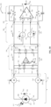
- FIG.3B shows an apparatus 375 for detecting optical signals.
- the apparatus 375 is the same as apparatus 300 with only difference that the apparatus 375 does not show the extra circuitry for transferring the ESD out of the detector circuit 202. does not show the capacitor 315, and does not show the RC filter coupled to the interface 392.
- the apparatus 375 includes the detector circuit 202 producing the photodetector current 365 and the current 363 that circulates in the apparatus 375.
- the apparatus 375 also includes the feedback circuit 204 having the Op-Amp 320 with the inverting node 326 coupled to the junction point 325, a voltage source, e.g.
- the apparatus 375 includes the amplifier circuit 208, which includes the Op-Amp 350 that works, e.g., is biased, in the linear region and, thus, the voltages of the non-inverting node 358 and the inverting node 356 are the same.
- FIG. 3C shows a circuit, e.g., a bias circuit 206, for reverse-biasing the photodetector 115.
- the bias circuit 206 of FIG. 3C provides the voltage sources 342 and 344.
- the bias circuit 206 of FIG. 3C which can be used as part of the apparatus 300, shows the interface 394, having the nodes 256 and 258, and the interface 396, having the nodes 262, 264, 266, and 268.
- the bias circuit 206 of FIG. 3C includes two operational-amplifiers, an Op-Amp 222, e.g., a first Op-Amp, and an Op-Amp 224, e.g. a second Op-Amp.
- Non-inverting nodes 228 and 246 of the Op-Amps 222 and 224 are respectively coupled to the nodes 256 and 258.
- the nodes 256 is coupled to the node 262 and the node 258 is coupled to the node 268.
- a current source 226 providing a current I o is coupled between the inverting node 232 of the Op-Amp 222 and the inverting node 244 of the Op-Amp 224.
- a resistor 212 and a resistor 214 are respectively coupled between the output node 238 of the Op-Amp 222 and the node 264, and coupled between the output node 242 of the Op-Amp 224 and the node 266.
- the resistors 212 and 214 are variable resistors.
- Capacitors 253 and 255 are respectively coupled between the nodes 262 and 264 and between the nodes 266 and 268.
- the RC time constant of the resistor 212/214 and the capacitor 253/255 is long enough to filter out any low frequency noise from Op-Amp 222 and Op-Amp 224, resistor 234/236 and current source 226.
- the bias circuit 206 includes a controller 310 that is coupled via control lines 340 and 345, e.g., connection lines, to the resistor 212 and the resistor 214, respectively, to control a value of resistor 212 and the resistor 214.
- the current I o of the current source 226 and the feedback resistor 234/236 crossing the Op-Amp 222 and the Op-Amp 224 builds a reverse-bias voltage and charges it to the capacitor 253 and 255 that produce voltages 257 and 259, respectively.
- the capacitors 253 and 255 are charged to a half of the reverse-bias voltage.
- the values of the resistors 234 and 236 and capacitors 253 and 255 are selected to be the same and the Op-Amps 222 and 224 have the same operating parameters.
- the voltages produced by the stored charges on the capacitors 253 and 255 have different magnitudes of up to twenty percent, however, the sum of the magnitude of the voltages 257 and 259 makes the photodetector 115 reverse-biased.
- the voltage 257 is consistent with the voltage 372 and the voltage 259 is consistent with the voltage 374.
- the controller 310 adjusts the resistor 212 and the resistor 214 such that the time constant of charging the capacitors 253 and 255 are adjusted.
- the voltages 257 and 259 of the capacitors 253 and 255 are determined by the current I o of the current source 226 and the feedback resistor 234/236 crossing the Op-Amp 222 and the Op-Amp 224.
- the resistor 212 and resistor 214 are implemented with field effect transistors (FET).
- the resistor 212 and resistor 214 are metal oxide semiconductor field effect transistors (MOSFET) that are biased in the weak inversion regions and the controller 310 adjusts the gate voltage of the FET or MOSFET, through the control lines 340 and 345, to change the resistance between drain and source of the transistor (R ds ).
- MOSFET metal oxide semiconductor field effect transistors
- the controller 310 adjusts the gate voltage of the FET or MOSFET, through the control lines 340 and 345, to change the resistance between drain and source of the transistor (R ds ).
- R ds metal oxide semiconductor field effect transistors
- the controller 310 senses the voltages 257 and 259, through the control line 355, and adjusts the resistor 212 and the resistor 214 to adjust the time constant of charging the capacitors 253 and 255 to reduce low frequency noise of the voltages 257 and 259.
- the recharging of the capacitors 253 and 255, due to charge leakage of the capacitors 253 and 255, is performed continuously and even when the apparatus 300 is detecting optical signals 112 and do not need to stop the detection.
- FIGS. 4A and 4B illustrate an amplifier circuit and a low noise amplifier circuit for the system for detecting optical signals, according to various aspects of the subject technology.
- FIG. 4A shows the amplifier circuit 400 that includes multiple stages and first stage that is a low noise amplifier (LNA).
- the amplifier circuit 400 may replace the Op-Amp 350 of FIGS. 3A , 3B , and 3C .
- the amplifier circuit 400 includes the LNA, e.g., an LNA 410, which receives the input signal 442.
- the input signal 442 is the photodetector current 365 of the photodetector 115.
- the LNA 410 is a resistive loaded amplifier.
- the resistor load has better linearity against EMI interference compared to transistors and also has a better low-frequency noise performance, as resistor has much lower flicker noise compared to transistors.
- this structure requires a higher input common mode voltage in order to achieve similar gain and thermal noise performance compared to a transistor load used in traditional amplifier structure.
- the higher input common mode is provided by the fully differential architecture discussed above.
- the LNA 410 provides enough gain, it may suppress the EMI interference and noise from going to the subsequent stages.
- a first output signal 452 at an output node 451 of the LNA 410 may be amplified by a dual-path three-stage amplifier composed of a first amplifier 420, a second amplifier 430, a feed forward amplifier 460 and a third amplifier 440 in some embodiments.
- the feed forward amplifier 460 that may amplify a wide band signal is used to amplify the first output signal 452 and to generate a second output signal 458.
- the first amplifier 420 receives the first output signal 452 and generates a third output signal 454.
- the third output signal 454 is filtered by a first capacitor 432, coupled between an output of the first amplifier 420 and a ground, to generate a fourth output signal 455.
- the second amplifier 430 receives the fourth output signal 455 and generates a fifth output signal 456.
- the fifth output signal 456 is added to the second output signal 458 by an adder module 462 to generate a signal 464.
- the third amplifier 440 receives the signal 464 and generates a sixth output signal 448 that is added, by an adder module 466, to the signal 447, which is the signal 464 that is filtered by a second compensation capacitor 434 that is in parallel with the third amplifier 440.
- the adder module 466 produces as an output signal 468 at an output node 467 of the amplifier circuit 400.
- the first capacitor 432 is used for frequency compensation of an Op-Amp of the amplifier circuit 400.
- FIG. 4B shows the LNA 410 that includes two p-type metal oxide semiconductor transistors, PMOS transistors 405 and 415. As shown, bulks of PMOS transistors 405 and 415 are coupled, via connection 425, to a common source node 406 of the PMOS transistors 405 and 415. Drains 408 and 412 of the PMOS transistors 405 and 415 are coupled, via a capacitor 418 together.
- FIG. 4A is single ended, but in some other embodiments it is differential.
- FIG. 4B shows the differential implementation of the LNA 410 whereby the gates 414 and 416 of the PMOS transistors 415 and 405 that correspond to a differential version of node 441 in FIG. 4A .
- the common source node 406 is coupled to a current source 404 and the current source 404 is coupled to a voltage node 402.
- the LNA 410 further includes two RC circuits coupled in parallel.
- a first RC circuit includes a resistor 426 coupled in parallel to a capacitor 428.
- a second RC circuit includes a resistor 424 coupled in parallel to a capacitor 422.
- Each one of the two RC circuits are coupled between the ground 114 and each end of the capacitor 418.
- LNA 410 includes the resistors 424 and 426 and, thus, generate thermal noise.
- the output of the LNA is a voltage between the drains 408 and 412 of the PMOS transistors 405 and 415, which is a differential version of output node 451 in FIG. 4A .
- the capacitors 428 and 422 provide a bypass for the EMI to the ground 114 and the capacitor 418 provides a bypass to balance a differential EMI.
- the subject technology discussed above provides a circuit for detecting an optical signal by using a photodetector.
- the circuit is designed to provide the fully differential signal paths and an input common-mode feedback such that input CMI rejection is achieved.
- a bias circuitry creates a differential voltage at circuit input to provide reverse-bias for a photodetector.
- the circuit uses capacitors that are charged continuously to provide the reverse bias of the photodetector while the circuit is detecting optical signals. Thus, the detection does not need to stop for re-charging the capacitors.
- an apparatus includes a photodetector and the photodetector is reverse-biased by a reverse-bias voltage (V RB ). Also, a common mode voltage (V o ) is added to the reverse-bias voltage to provide an offset to both an anode and a cathode of the photodetector.
- the apparatus also includes a first circuit coupled to the photodetector to provide the common mode voltage to the photodetector and a second circuit coupled to the first circuit that includes a first voltage source and a second voltage source that provide the reverse-bias voltage for the photodetector.
- Each one of the first voltage source and the second voltage source are coupled to one of the anode or the cathode of the photodetector.
- the second circuit receives a current of the photodetector via the first circuit and provides the current of the photodetector at an output of the second circuit.
- the first circuit includes a third voltage source to generate the common mode voltage.
- the first circuit includes an operational-amplifier (Op-Amp) such that an inverting node of the Op-Amp is coupled to a first node between first and second capacitors of the first circuit and an output node of the Op-Amp is coupled to a second node between third and fourth capacitors of the first circuit.
- the third voltage source is coupled between a non-inverting node of the Op-Amp and a ground to provide the common mode voltage to the non-inverting node of the Op-Amp.
- the apparatus further includes a third circuit that include a low noise amplifier and is coupled to the second circuit to amplify the current of the photodetector, received from the photodetector via the first circuit and the second circuit and to provide an output voltage proportional to the current of the photodetector.
- the first, second, and third circuits provide differential signal paths.
- the second circuit provides the reverse-bias voltage, via the first circuit to the photodetector. The second circuit receives the current of the photodetector via the first circuit.
- voltages at the cathode and the anode of the photodetector are set at V o + 1/2V RB and V o - 1/2V RB respectively.
- an apparatus includes a first circuit that includes a first port, a second port, and a third voltage source to provide a common mode voltage (V o ).
- the first circuit receives a current at the first port, receives first and second bias voltages having opposite polarities at first and second nodes of the second port and the common mode voltage is added to the first and second bias voltages as an offset, and provides the first bias voltage plus the common mode voltage and the second bias voltage plus the common mode voltage at the first and second nodes of the first port.
- the apparatus also includes a second circuit, coupled to the second port of the first circuit.
- the second circuit includes a first voltage source that provides the first bias voltage and a second voltage source that provides the second bias voltage. Each one of the first voltage source and the second voltage source are coupled between separate input and output nodes of input and output ports of the second circuit.
- the second circuit receives the current from the first circuit and provides the current.
- the apparatus further includes a third circuit coupled to the second circuit that receives the current, amplifies the current, and provides an output voltage proportional to the current.
- the first, second, and third circuits provide fully differential signal paths.
- the apparatus further includes a photodetector coupled to the first port. The first bias voltage plus the common mode voltage and the second bias voltage plus the common mode voltage are applied to a cathode and an anode of the photodetector to reverse-bias the photodetector by a sum of magnitudes of the first and second bias voltages (VRB).
- the first bias voltage plus the common mode voltage is presented as V o + 1/2V RB that is applied to the cathode of the photodetector
- the second bias voltage plus the common mode voltage is presented as V o - 1/2V RB that is applied to the cathode of the photodetector.
- the photodetector is reverse-biased by the sum of the magnitudes of the first and second bias voltages.
- the first circuit filters an electromagnetic interference, received by the first and second nodes of the first port, and prevents the electromagnetic interference outside a frequency band of the current from reaching the third circuit.
- an apparatus includes a first circuit that includes a photodetector and a second circuit coupled to the first circuit that includes a first voltage source that provides a common mode voltage (V o ).
- the apparatus also includes a third circuit coupled the second circuit that includes a first capacitor and a second capacitor.
- the first capacitor and the second capacitor are charged to a first voltage (V 1 ) and a second voltage (V 2 ).
- the first capacitor and the second capacitor provide the first voltage and the second voltage to the first circuit to be coupled to an anode and a cathode of the photodetector to reverse-bias the photodetector and the common mode voltage is applied to both the anode and the cathode of the photodetector.
- the photodetector is reverse-biased by a sum (V RB ) of magnitudes of the first and second voltages
- bias voltages at the cathode and the anode of the photodetector are set to V o + 1/2V RB and V o - 1/2V RB respectively
- voltages at first and second nodes of a first interface between the third circuit and the second circuit are set to V o + 1/2V RB and V o - 1/2V RB respectively
- voltages at the first and second nodes of a second interface between the second circuit and the first circuit are set to V o + 1/2V RB and V o - 1/2V RB respectively.
- the apparatus further includes a fourth circuit coupled to the third circuit and to amplify a current of the photodetector, received via the second circuit and the third circuit, and provide an output voltage proportional to the current of the photodetector.
- the second circuit filters an electromagnetic interference, received by the first circuit, and prevents the electromagnetic interference from reaching the fourth circuit.
- the third circuit further includes first and second variable resistors, first and second operational-amplifiers (Op-Amp), third and fourth resistors such that each one of the third and fourth resistors is coupled between an inverting node and output node of one of the first and second Op-Amps, and a current source for charging the first capacitor and the second capacitor.
- the first and second variable resistors are used to adjust time constants of charging the first capacitor and the second capacitor.
- the first and the second variable resistors are implemented by metal oxide semiconductor field effect transistors in weak inversion region to increase resistances of the first and the second variable resistors and to reduce thermal noise.
- any specific order or hierarchy of blocks in the processes disclosed is an illustration of example approaches. Based upon design preferences, it is understood that the specific order or hierarchy of blocks in the processes may be rearranged, or that all illustrated blocks should be performed. Any of the blocks may be simultaneously performed. In one or more implementations, multitasking and parallel processing may be advantageous. Moreover, the separation of various system components in the embodiments described above should not be understood as requiring such separation in all embodiments, and it should be understood that the described program components and systems could generally be integrated together in a single software product or packaged into multiple software products.
- base station As used in this specification and any claims of this application, the terms “base station,” “receiver,” “computer,” “server,” “processor,” and “memory” all refer to electronic or other technological devices. These terms exclude people or groups of people.
- display or “displaying” means displaying on an electronic device.
- the phrase "at least one of” preceding a series of items, with the term “and” or “or” to separate any of the items, modifies the list as a whole, rather than each member of the list (i.e., each item).
- the phrase "at least one of” does not require selection of at least one of each item listed; rather, the phrase allows a meaning that includes at least one of any one of the items, and/or at least one of any combination of the items, and/or at least one of each of the items.
- phrases “at least one of A, B, and C” and “at least one of A, B, or C” each refer to only A, only B, or only C; any combination of A, B, and C; and/or at least one of each of A, B, and C.
- a processor configured to monitor and control an operation or a component may also mean the processor being programmed to monitor and control the operation or the processor being operable to monitor and control the operation.
- a processor configured to execute code can be construed as a processor programmed to execute code or operable to execute code.
- phrases such as “an aspect,” “the aspect,” “another aspect,” “some aspects,” “one or more aspects,” “an implementation,” “the implementation,” “another implementation,” “some implementations,” “one or more implementations,” “an embodiment,” “the embodiment,” “another embodiment,” “some embodiments,” “one or more embodiments,” “a configuration,” “the configuration,” “another configuration,” “some configurations,” “one or more configurations,” “the subject technology,” “the disclosure,” “the present disclosure,” and other variations thereof and alike are for convenience and do not imply that a disclosure relating to such phrase(s) is essential to the subject technology or that such disclosure applies to all configurations of the subject technology. A disclosure relating to such phrase(s) may apply to all configurations, or one or more configurations. A disclosure relating to such phrase(s) may provide one or more examples.
- a phrase such as “an aspect” or “some aspects” may refer to one or more aspects and vice versa, and this applies similarly to other foregoing phrases.
Landscapes
- Engineering & Computer Science (AREA)
- Power Engineering (AREA)
- Physics & Mathematics (AREA)
- General Physics & Mathematics (AREA)
- Spectroscopy & Molecular Physics (AREA)
- Electromagnetism (AREA)
- Computer Networks & Wireless Communication (AREA)
- Signal Processing (AREA)
- Amplifiers (AREA)
Abstract
Description
- The present description relates generally to receivers for optical sensing, including optical detectors, and in particular, to reduction of interference including radio frequency (RF) interference.
- Optical sensing devices that include optical detectors are used for sensing optical signals. Optical signals may be weak and require amplification up to a hundred times or more by amplifier circuits. Electronic circuits including optical sensing devices are prone to electromagnetic interference. Thus, interference signals caused by electromagnetic interference may be added to the optical signal and amplified, up to a hundred times or more, by the amplifier circuits and contaminate the optical signals. Therefore, it is highly desirable to minimize the interference signal before being added to the optical signals and before the optical signal is amplified.
- According to an aspect, an apparatus is provided comprising:
- a photodetector, wherein the photodetector is reverse-biased by a reverse-bias voltage (VRB), and wherein a common mode voltage (Vo) is added to the reverse-bias voltage to provide an offset to both an anode and a cathode of the photodetector;
- a first circuit coupled to the photodetector and configured to provide the common mode voltage to the photodetector; and
- a second circuit coupled to the first circuit that comprises a first voltage source and a second voltage source and configured to provide the reverse-bias voltage for the photodetector, wherein each one of the first voltage source and the second voltage source are coupled to one of the anode or the cathode of the photodetector, wherein the second circuit is configured to receive a current of the photodetector via the first circuit and to provide the current of the photodetector at an output of the second circuit.
- Advantageously, the first circuit comprises a third voltage source configured to generate the common mode voltage.
- Advantageously, the first circuit comprises:
an operational-amplifier (Op-Amp), wherein an inverting node of the Op-Amp is coupled to a first node between first and second capacitors of the first circuit, an output node of the Op-Amp is coupled to a second node between third and fourth capacitors of the first circuit, and the third voltage source is coupled between a non-inverting node of the Op-Amp and a ground to provide the common mode voltage to the non-inverting node of the Op-Amp. - Advantageously, the apparatus further comprises:
a third circuit that comprises a low noise amplifier is coupled to the second circuit and is configured to amplify the current of the photodetector, received from the photodetector via the first circuit and the second circuit and provide an output voltage proportional to the current of the photodetector. - Advantageously, the first, second, and third circuits provide differential signal paths.
- Advantageously, the second circuit is configured to provide the reverse-bias voltage, via the first circuit to the photodetector, and wherein the second circuit is configured to receive the current of the photodetector via the first circuit.
- Advantageously, voltages at the cathode and the anode of the photodetector are set at Vo + 1/2VRB and Vo - 1/2VRB respectively.
- According to an aspect, an apparatus is provided comprising:
- a first circuit comprising a first port, a second port, and a third voltage source configured to provide a common mode voltage (Vo), the first circuit is configured to:
- receive a current at the first port,
- receive first and second bias voltages having opposite polarities at first and second nodes of the second port, wherein the common mode voltage is added to the first and second bias voltages as an offset, and
- provide the first bias voltage plus the common mode voltage and the second bias voltage plus the common mode voltage at the first and second nodes of the first port; and
- a second circuit, coupled to the second port of the first circuit, the second circuit that comprises a first voltage source configured to provide the first bias voltage and a second voltage source configured to provide the second bias voltage, wherein each one of the first voltage source and the second voltage source are coupled between separate input and output nodes of input and output ports of the second circuit.
- Advantageously, the second circuit is configured to receive the current from the first circuit and to provide the current, the apparatus further comprising:
a third circuit coupled to the second circuit and configured to receive the current, amplify the current, and provide an output voltage proportional to the current. - Advantageously, the first, second, and third circuits provide fully differential signal paths.
- Advantageously, the apparatus further comprises:
a photodetector coupled to the first port, wherein the first bias voltage plus the common mode voltage and the second bias voltage plus the common mode voltage are applied to a cathode and an anode of the photodetector to reverse-bias the photodetector by a sum of magnitudes of the first and second bias voltages (VRB). - Advantageously, the first bias voltage plus the common mode voltage is presented as Vo + 1/2VRB that is applied to the cathode of the photodetector, and wherein the second bias voltage plus the common mode voltage is presented as Vo - 1/2VRB that is applied to the cathode of the photodetector.
- Advantageously, the photodetector is reverse-biased by the sum of the magnitudes of the first and second bias voltages.
- Advantageously, the first circuit is configured to filter an electromagnetic interference, received by the first and second nodes of the first port, and prevent the electromagnetic interference, outside a frequency band of the current, from reaching the third circuit.
- According to an aspect, an apparatus is provided comprising:
- a first circuit that comprises a photodetector;
- a second circuit coupled to the first circuit and comprising a first voltage source that provides a common mode voltage (Vo); and
- a third circuit coupled the second circuit that comprises a first capacitor and a second capacitor, wherein the first capacitor and the second capacitor are configured to be charged to a first voltage (V1) and a second voltage (V2), wherein the first capacitor and the second capacitor are configured to provide the first voltage and the second voltage to the first circuit to be coupled to an anode and a cathode of the photodetector to reverse-bias the photodetector, and wherein the common mode voltage is applied to both the anode and the cathode of the photodetector.
- Advantageously:
- the photodetector is reverse-biased by a sum (VRB) of magnitudes of the first and second voltages,
- bias voltages at the cathode and the anode of the photodetector are set to Vo + 1/2VRB and Vo - 1/2VRB respectively,
- voltages at first and second nodes of a first interface between the third circuit and the second circuit are set to Vo + 1/2VRB and Vo - 1/2VRB respectively, and
- voltages at the first and second nodes of a second interface between the second circuit and the first circuit are set to Vo + 1/2VRB and Vo - 1/2VRB, respectively.
- Advantageously, the apparatus further comprises:
a fourth circuit coupled to the third circuit and configured to amplify a current of the photodetector, received via the second circuit and the third circuit, and provide an output voltage proportional to the current of the photodetector. - Advantageously, the second circuit is configured to filter an electromagnetic interference, received by the first circuit, and prevent the electromagnetic interference from reaching the fourth circuit.
- Advantageously, the third circuit further comprises:
- first and second variable resistors;
- first and second operational-amplifiers (Op-Amps);
- third and fourth resistors, wherein each one of the third and fourth resistors is coupled between an inverting node and output node of one of the first and second Op-Amps; and
- a current source configured to charge the first capacitor and the second capacitor, wherein the first and second variable resistors are used to adjust time constants of charging the first capacitor and the second capacitor.
- Advantageously, the first and the second variable resistors are implemented by metal oxide semiconductor field effect transistors in weak inversion region to increase resistances of the first and the second variable resistors and to reduce thermal noise.
- Certain features of the subject technology are set forth in the appended claims. However, for purposes of explanation, several aspects of the subject technology are depicted in the following figures.
-
FIG. 1 illustrates an apparatus for detecting and processing optical signals. -
FIG. 2 illustrates an apparatus for detecting optical signals, according to various aspects of the subject technology. -
FIGS. 3A ,3B , and3C illustrate an apparatus for detecting optical signals, an apparatus for detecting optical signals and with protection against electrostatic discharge, and a circuit for reverse-biasing a photodetector, according to various aspects of the subject technology. -
FIGS. 4A and 4B illustrate an amplifier circuit and a low noise amplifier circuit for the apparatus for detecting optical signals, according to various aspects of the subject technology. - The detailed description set forth below is intended as a description of various configurations of the subject technology and is not intended to represent the only configurations in which the subject technology may be practiced. The appended drawings are incorporated herein and constitute part of the detailed description, which includes specific details for providing a thorough understanding of the subject technology. However, the subject technology is not limited to the specific details set forth herein and may be practiced without one or more of the specific details. In some instances, structures and components are shown in a block-diagram form in order to avoid obscuring the concepts of the subject technology.
- When an element is referred to herein as being "connected" or "coupled" to another element, it is to be understood that the elements can be directly connected to the other element, or have intervening elements present between the elements. In contrast, when an element is referred to as being "directly connected" or "directly coupled" to another element, it should be understood that no intervening elements are present in the "direct" connection between the elements. However, the existence of a direct connection does not exclude other connections, in which intervening elements may be present.
- A circuit for detecting optical signals may have closed loops and, thus, electromagnetic interference, e.g., radio frequency (RF) electromagnetic (EM) interference, e.g., electromagnetic signals induced by power lines and devices using alternating current, in the environment may generate currents and voltages in the closed loops of the circuit and may impact the detected signals. In some embodiments, the detected optical signals produce low currents and voltages that require considerable amplification of hundred times or more to increase the detected signal to a voltage or current level that may be digitized and then processed. Because the electromagnetic interference is added to the detected signal before amplification, the amplification may also amplify the electromagnetic interference the same way that the detected optical signal is amplified. The circuits and apparatuses introduced below provide fully differential architectures for signal paths and have a very good interference rejection because of the symmetric structure. The interference affects both signal paths (positive and negative) nearly the same, so when the negative signal is subtracted from the positive signal, the interference on both signals cancels each other. Thus, the fully differential signal paths may cause the common-mode interference (CMI) to be subtracted between positive and negative output nodes and, thus, the CMI is rejected and RF electromagnetic (EM) interference and electrostatic discharge (ESD) effects are reduced. In addition, the circuit for detecting optical signals may reverse-bias a photodetector of the circuit for detecting optical signals and also may provide a common mode voltage, e.g., an offset voltage, to increase the dynamic range and prevent non-linearity, e.g., clipping from top or bottom. In some embodiments, the fully differential signal paths opens the possibility of increasing the common mode voltage to about half the supply rails. Higher common mode voltages reduce the non-linearity produced by ESD protection circuit and EMI due to balance swing, e.g., caused by reverse-biased diodes that are used for ESD protection. In some embodiments, the optical signal is a periodic signal and the detected signal is a periodic voltage. The common mode voltage may be adjusted based on induced currents such that the detected current of the photodetector and the detected output voltage are not clipped from top or bottom. In some embodiments, the circuits, devices, and systems introduced below that provide a differential architecture, e.g., a fully differential architecture, reduces the input referred current detection error, induced by the CMI, to more than two orders of magnitude lower compared to circuits that do not have the fully differential architecture. The EMI impinging on the ESD diodes may be partially rectified by the ESD diodes out of the
detector circuit 202 and partially remain and generate a current in thedetector circuit 202 that is not from photodetector, causing error in theapparatus 300. -
FIG. 1 illustrates an apparatus for detecting and processing optical signals. Anapparatus 100 ofFIG. 1 shows acircuit 130, e.g., a circuit for detecting optical signals, which includes aphotodetector 115 coupled between avoltage node 111 and aground 114. As shown, ananode 106 of thephotodetector 115 is coupled to theground 114 and acathode 108 of thephotodetector 115 is coupled to thevoltage node 111. In some embodiments, In some embodiments, a voltage V1 of thevoltage node 111 is forced, e.g., induced, by theamplifier unit 102 and, thus, thephotodetector 115 is reverse-biased by the voltage V1. In some embodiments, thephotodetector 115 is a diode that is reverse-biased and anoptical signal 112, e.g., light rays, impinge on a depletion region (not shown) of thephotodetector 115 to generate charge carriers proportional to an intensity of the light rays. In some embodiments, the charged carriers are determined to be proportional to the intensity of the light rays and by increasing the intensity of the light rays by n times, where n is 2, 3, ..., the number of charged carriers is increased by n times. The generated charge carriers, produce a current 120, e.g., an input signal, by thephotodetector 115. In some embodiments, the voltage V1 is between about 0 volts and 10 volts. In some embodiments, in a reverse-biased diode a voltage coupled to the cathode of the diode is higher than the voltage coupled to an anode of the diode. In some embodiments, thephotodetector 115 is a diode that is reverse-biased. - As shown in
FIG. 1 , theapparatus 100 also includes anamplifier unit 102, a data acquisition unit, e.g., aDA unit 104, and a digital signal processing unit, e.g., aDSP unit 107. The current 120 or a voltage generated by the current 120 and proportional to the current 120 is amplified by theamplifier unit 102. In some embodiments, theamplifier unit 102 amplifies the input signal several folds, e.g., a hundred times or more, to produce anoutput signal 122, e.g., a voltage, which is used by theDA unit 104. - As shown in
FIG. 1 , in some embodiments, an EM interference (EMI), e.g.,EMI 110, is present in an environment of thecircuit 130 of theapparatus 100. TheEMI 110 may induce an interference current in thecircuit 130 that is amplified along with the current 120 and is similarly added, as an interference signal, to the output signal of theamplifier unit 102 and, thus, theoutput signal 122 includes the interference signal. Theoutput signal 122 of theamplifier unit 102 is received by theDA unit 104, as an input signal, to produce anoutput signal 124 of theDA unit 104. In some embodiments, theDA unit 104 digitizes, by an analog to digital converter (not shown), the input signal and, thus, theoutput signal 124 is a digitized form of theoutput signal 122. Theoutput signal 124 is then fed into theDSP unit 107 for processing and to generate anoutput signal 125. -
FIG. 2 illustrates an apparatus for detecting optical signals, according to various aspects of the subject technology. In some embodiments, anapparatus 200 ofFIG. 2 shows is a combination of thecircuit 130 and theamplifier unit 102 ofFIG. 1 . As shown, theapparatus 200 includes adetector circuit 202 that includes thephotodetector 115. Theapparatus 200 also includes afeedback circuit 204, abias circuit 206, and anamplifier circuit 208 that generates an output, e.g., anoutput voltage 360. Thedetector circuit 202 is coupled to thefeedback circuit 204 through aninterface 392. Thefeedback circuit 204 is coupled to thebias circuit 206 through aninterface 394 and thebias circuit 206 is coupled theamplifier circuit 208 through aninterface 396. Theinterfaces interfaces detector circuit 202, thefeedback circuit 204, thebias circuit 206, theamplifier circuit 208, and theinterfaces FIGS. 3A ,3B , and3C .FIG. 2 also shows that theEMI 110 may affect thedetector circuit 202 and may generate an EMI current, e.g., a current 215, in thedetector circuit 202. In some embodiments, thefeedback circuit 204 is used to filter the EMI and prevents the EMI, e.g., the EMI outside the frequency band of theoptical signal 112, from reaching theamplifier circuit 208 coupled to thebias circuit 206. In some embodiments, theamplifier circuit 208 receives a current 363 via thefeedback circuit 204 and thebias circuit 206. In some embodiments, theresistors capacitors resistors capacitors photodetector current 365. Thus, in some embodiments, theamplifier circuit 208 amplifies the photodetector current 365 to provide theoutput voltage 360 that is proportional to thephotodetector current 365. In some embodiments, theoutput voltage 360 is determined to be proportional to the photodetector current 365 and by increasing the photodetector current 365 by n (e.g., n = 2, 3, etc.) times, theoutput voltage 360 is also increased by n times. In some embodiments, the currents through theresistors amplifier circuit 208 amplifies the current 363, anoutput voltage 360 may be provided that is proportional to the photodetector current 365 plus a voltage bias such that the voltage bias may limit a dynamic range of theoutput voltage 360. - In some embodiments, by receiving a voltage at an interface coupled between two circuits, e.g., between circuit-A and circuit-B, the circuit-A provides, e.g., delivers, the voltage at the interface and the circuit-B receives the voltage at the interface. Thus, in some embodiments, the interface is an output port of the circuit-A and also is an input port of the circuit-B. Also, in some embodiments, the output port of the circuit-A and the input port of the circuit-B are coupled through two nodes, e.g., node-1 and node-2. In some embodiments, by receiving a current at the interface coupled between circuit-A and circuit-B, the circuit-A provides, e.g., delivers, the current at the node-1 of the interface and the circuit-B receives the current at the node-1 of the interface.
-
FIGS. 3A ,3B , and3C illustrate apparatuses for detecting optical signals and a circuit for reverse-biasing a photodetector, according to various aspects of the subject technology.FIG.3A shows theapparatus 300 for detectingoptical signals 112 that impinge on thephotodetector 115. In some embodiments, the optical signal are optical pulses that are detected by thephotodetector 115. In some embodiments, as described, thephotodetector 115 is reverse-biased and, thus, a voltage between both ends of thephotodetector 115, which is between acathode 308 and ananode 306 of thephotodetector 115, is a positive voltage. In some embodiments, as noted above, avoltage 366, e.g., a reverse-bias voltage VPD of thephotodetector 115 is between about 0 volts and about 10 volts. In some embodiments, the reverse-bias voltage VPD is applied in a symmetrical form such that half of the reverse-bias voltage, which is 1/2VPD is applied to thecathode 308 and -1/2VPD is applied to theanode 306. - In some embodiments, as shown, a
capacitor 315 is coupled in parallel with thephotodetector 115. As shown, in response to theoptical signal 112 impinging on thephotodetector 115, a photodetector current 365 is generated by thephotodetector 115 in thedetector circuit 202, e.g., a first circuit. In some embodiments, thecapacitor 315 is used to cause a short-circuit parallel to thephotodetector 115 for the current and/or voltage fluctuations, e.g., high frequency fluctuations, and prevent the fluctuation to impact thephotodetector 115. In some embodiments, ground bouncing interference to thephotodetector 115 is absorbed by thecapacitor 315 and the fully differential structure of theapparatus 300 is maintained. - The
detector circuit 202 is further coupled to a first group of ESD diodes D1 and D2 and to a second group of ESD diodes D3 and D4. The diode D1 is coupled and reverse-biased between thecathode 308 and thevoltage node 116, which has a positive voltage between about 2 volts and 5 volts above the voltage of thecathode 308. The diode D2 is coupled and reverse-biased between thecathode 308 and theground 114. In some embodiments, the diodes D1 and D2 are reverse-biased diodes that are used for preventing a damage to theapparatus 300 because of the electrostatic discharge (ESD). In some embodiments, the diodes D1 and D2 transfer at least a part of the ESD, out of thedetector circuit 202. Similarly, in some embodiments, the diode D3 is coupled and reverse-biased between theanode 306 and avoltage node 117, which has a positive voltage between about 2 volts and 5 volts above the voltage of theanode 306. The diode D4 is coupled and reverse-biased between theanode 306 and theground 114. In some embodiments, the reverse-biased diodes D1 and D2 are coupled to thedetector circuit 202 and adjacent to thecathode 308, and also reverse- biased diodes D3 and D4 are coupled to thedetector circuit 202 and adjacent to theanode 306 and are used for preventing a damage to circuit components of theapparatus 300 due to electrostatic discharge (ESD) and transferring the ESD, e.g., at least part of the ESD, out of thedetector circuit 202. The EMI induced on the detector circuit may be rectified by the ESD diodes and because of the non-linearity of the ESD diodes may cause a current in thedetector circuit 202, which is not from photodetector, causing error in theapparatus 300. In some embodiments, the symmetrical configuration of the first and second groups of diodes helps balance the non-linearity on invertingnode 326 andnon-inverting node 328 of an operational-amplifier, Op-Amp 320, of thefeedback circuit 204. - In addition to the ESD, as described above, the
detector circuit 202 may be affected by the EMI from a power line, a neighboring device or circuit, and as shown inFIG. 1 , theEMI 110 may generate an additional current, the current 215 in thedetector circuit 202 such that the current 215 is added to thephotodetector current 365 of thephotodetector 115. Although, the current 215 is induced in thedetector circuit 202, because theapparatus 300 provides fully differential signal paths,FIG. 3A shows that the addition of current 215, which is induced may conceptually be represented by theaddition modules apparatus 300 and is rejected, e.g., removed, by the fully differential structure of theapparatus 300. In some embodiments, the current 215 includes the current caused by the non-linearity of the ESD diodes as described before. In some embodiments, the first group of ESD diodes are physically close to about half of the source of the ESD and the second group of ESD diodes are physically close to another half of the source of the ESD. In some embodiments, a combination of thefeedback circuit 204, thebias circuit 206, and theamplifier circuit 208 provides the fully differential signal paths. - As shown in
FIG. 3A , thedetector circuit 202 is connected tofeedback circuit 204 through theinterface 392 at an output of thedetector circuit 202 and an input of thefeedback circuit 204, which provides the common mode voltage for the reverse-biasedphotodetector 115. Theinterface 392 includes the twonodes nodes feedback circuit 204 includes a first RC circuit that includes aresistor 316, e.g., a first resistor, and aresistor 318, e.g., a second resistor coupled, in series, coupled to theinterface 392 between thenodes capacitor 322, e.g., a first capacitor, and acapacitor 324, e.g., a second capacitor coupled to theinterface 392 between thenodes resistor 316 and theresistor 318 and the midpoint between thecapacitor 322 and thecapacitor 324 are connected to each other to provide ajunction point 325, e.g., a first junction point or a first node. In some embodiments, theinterface 392 is an output port of thedetector circuit 202 and is an input port of thefeedback circuit 204. In some embodiments, theinterfaces interfaces - In addition, the
capacitor 322 is coupled in parallel with theresistor 316 between thenode 252 and thejunction point 325 and thecapacitor 324 is coupled in parallel with theresistor 318 between thejunction point 325 and thenode 254. In some embodiments, values of theresistor 316 and theresistor 318 and the values of thecapacitor 322 and thecapacitor 324 are selected such that the values do not affect the photodetector signal being processed. Also, the high frequency noise and interferences outside a frequency band of theoptical signal 112 are short circuited by thecapacitor 322 and thecapacitor 324 and do not move from thedetector circuit 202 beyond thefeedback circuit 204. In some embodiments, as shown inFIG. 3A , thedetector circuit 202 of theapparatus 300 also includes an RC filter, e.g., a low-pass filter, coupled to theinterface 392. As shown, acapacitor 314 of the RC filter is coupled between thenodes resistors nodes addition modules resistors apparatus 300 is maintained, e.g., have same values. In some embodiments, the low-pass RC filter is designed and thecapacitor 314 and theresistors optical signal 112. - The
feedback circuit 204 is connected to thebias circuit 206 through theinterface 394 at an output of thefeedback circuit 204 and an input of thebias circuit 206. Thefeedback circuit 204 includes a second RC circuit that includes aresistor 336, e.g., a first resistor of the second RC circuit, and aresistor 338, e.g., a second resistor, of the second RC circuit coupled, in series, to theinterface 394 between the twonodes interface 394. Similarly, voltages or currents are shared or transferred through thenodes feedback circuit 204 and thebias circuit 206. In addition, acapacitor 332, e.g., a first capacitor of the second RC circuit, is coupled in parallel with theresistor 336 between thenode 256 and a junction point 335, e.g., a second junction point or a second node, and a capacitor 334, e.g., a second capacitor of the second RC circuit, is coupled in parallel with theresistor 338 between the junction point 335 and thenode 258. In some embodiments, theresistor 336 and theresistor 338 have the same value, which is similar to the value of theresistor 316 or theresistor 318 of the first RC circuit. In some embodiments, thecapacitor 332 and the capacitor 334 have the same value, which is similar to the value of thecapacitor 322 or thecapacitor 324 of the first RC circuit. - As shown in
FIG. 3A , thefeedback circuit 204 further includes the Op-Amp 320, such that an invertingnode 326 of the Op-Amp 320 is connected to thejunction point 325 and an output node of the Op-Amp 320 is connected to the junction point 335. Also, the common mode voltage Vo (e.g., the offset voltage) is coupled between anon-inverting node 328 of the Op-Amp 320 and theground 114. As noted above, thebias circuit 206 is connected to thefeedback circuit 204 through theinterface 394 described above. Thebias circuit 206 includesvoltage sources photodetector 115. In some embodiments, VPD is the same as a reverse-bias voltage VRB of thephotodetector 115 between thecathode 308 and theanode 306 of thephotodetector 115. Thus, in some embodiments, thevoltage sources voltage sources FIG. 3C . In some embodiments, the Op-Amp 320 works, e.g., is biased, in the linear region and the voltage of the invertingnode 326 and the voltage of thenon-inverting node 328 are equal. In some embodiments, avoltage source 342 provides avoltage 372 for thecathode 308 and avoltage source 344 provides avoltage 374 for theanode 306. In some embodiments, the common mode voltage Vo and thephotodetector 115 voltage VPD at eachcathode 308 oranode 306 may independently change. In some embodiments, the common mode voltage Vo changes between 0.5 volts and 10 volts and thephotodetector 115 voltage VPD changes between zero volts and 10 volts. - In some embodiments, the common mode voltage Vo, e.g., about the same voltage, is added to the voltage of the
cathode 308 and theanode 306 of thephotodetector 115 and the sum voltage is applied to thecathode 308 and theanode 306. Thus, a voltage VA of theanode 306 and a voltage Vc of thecathode 308 may respectively be presented by equations (1) and (2).

- Thus, the common mode voltage Vo is applied as a common offset to both
anode 306 and thecathode 308 and the voltage across thephotodetector 115 is VPD. The voltage Vo or VPD in equations (1) or (2) may independently change by up to ten folds and still the voltage of theanode 306 and the voltage of thecathode 308 may be represented by equations (1) and (2) with modified common mode and photodetector voltages. Theapparatus 300 will provide the fully differential paths, if the modified common mode and photodetector voltages are within an acceptable range. In some embodiments, an output voltage of the Op-Amp 320 is proportional to the voltage of thenon-inverting node 328 minus the voltage of the invertingnode 326. Thus, the voltage of the invertingnode 326 is multiplied by negative one and then is added to the voltage of thenon-inverting node 328. In some embodiments, in the linear region, the Op-Amp 320 has a gain K between a thousand and ten thousand such that the output voltage of Op-Amp 320 is K times the input voltage, which is the voltage difference between thenon-inverting node 328 and the invertingnode 326. Since the output voltage of the Op-Amp 320 is limited by the voltage sources of the Op-Amp 320 that are about 2 to 15 volts, the input voltage of the Op-Amp 320 is very small and about zero volts. Therefore, when the Op-Amp 320 operates in the linear region, the non-inverting and invertingnodes Amp 320 may be assumed to have the same voltage. In some embodiments, as shown by equations (1) and (2), the common mode voltage Vo is an offset voltage to both theanode 306 and thecathode 308. - As shown, the
apparatus 300 also includes theamplifier circuit 208 that is coupled to thebias circuit 206 through theinterface 396 and vianodes interface 396. Thevoltage source 342, e.g., a first voltage source, is coupled between thenode 264 and thenode 256 and supplies avoltage 372, which is 1/2VPD. Thevoltage source 344, e.g., a second voltage source, is coupled between thenode 266 and thenode 258 and supplies avoltage 374, in an opposite direction of thevoltage 372, which is 1/2VPD. - As noted above, the
amplifier circuit 208 is coupled to thebias circuit 206 via theinterface 396 and through thenodes interface 396. Theamplifier circuit 208 includes an Op-Amp 350 with anon-inverting node 358 coupled to thenode 266 and an invertingnode 356 coupled to thenode 264. The Op-Amp 350 includes apositive output node 362 and anegative output node 364. Aresistor 352 and acapacitor 346 are coupled in parallel between thepositive output node 362 and thenode 262 of theinterface 396. Also, aresistor 354 and acapacitor 348 are coupled in parallel betweennegative output node 364 and thenode 268 of theinterface 396. - Because the
apparatus 300 provides fully differential signal paths, values of thecapacitors apparatus 300. Also, theresistors amplifier circuit 208. As shown, in some embodiments, a voltage between thepositive output node 362 and thenegative output node 364 of the Op-Amp 350 is an output voltage 360 (Vout) of theapparatus 300. In some embodiments, the Op-Amp 350 works, e.g., is biased, in the linear region of an Op-Amp and, thus, the voltage of the invertingnode 356 is equal to the voltage of thenon-inverting node 358. Therefore, the sum of the voltages of thevoltage source 342 and thevoltage source 344 will be applied on thephotodetector 115 and thevoltage 366 is equal to the sum of the voltages of thevoltage source 342 and thevoltage source 344, which is the voltage VPD and is the reverse-bias voltage VRB of thephotodetector 115. -
FIG.3B shows anapparatus 375 for detecting optical signals. Theapparatus 375 is the same asapparatus 300 with only difference that theapparatus 375 does not show the extra circuitry for transferring the ESD out of thedetector circuit 202. does not show thecapacitor 315, and does not show the RC filter coupled to theinterface 392. Theapparatus 375 includes thedetector circuit 202 producing the photodetector current 365 and the current 363 that circulates in theapparatus 375. Theapparatus 375 also includes thefeedback circuit 204 having the Op-Amp 320 with the invertingnode 326 coupled to thejunction point 325, a voltage source, e.g. a common mode voltage reference, providing the common mode voltage Vo is applied to thenon-inverting node 328, and an output node of the Op-Amp 320 is coupled to the junction point 335. Theapparatus 375 includes theamplifier circuit 208, which includes the Op-Amp 350 that works, e.g., is biased, in the linear region and, thus, the voltages of thenon-inverting node 358 and the invertingnode 356 are the same. -
FIG. 3C shows a circuit, e.g., abias circuit 206, for reverse-biasing thephotodetector 115. In some embodiments, thebias circuit 206 ofFIG. 3C provides thevoltage sources bias circuit 206 ofFIG. 3C , which can be used as part of theapparatus 300, shows theinterface 394, having thenodes interface 396, having thenodes bias circuit 206 ofFIG. 3C includes two operational-amplifiers, an Op-Amp 222, e.g., a first Op-Amp, and an Op-Amp 224, e.g. a second Op-Amp.Non-inverting nodes Amps nodes nodes 256 is coupled to thenode 262 and thenode 258 is coupled to thenode 268. As shown, acurrent source 226 providing a current Io is coupled between the invertingnode 232 of the Op-Amp 222 and the invertingnode 244 of the Op-Amp 224. Aresistor 234, e.g., a first resistor, is coupled between the invertingnode 232 and anoutput node 238 of the Op-Amp 222 and aresistor 236, e.g., a second resistor, is coupled between the invertingnode 244 and anoutput node 242 of the Op-Amp 224. As shown, aresistor 212 and aresistor 214 are respectively coupled between theoutput node 238 of the Op-Amp 222 and thenode 264, and coupled between theoutput node 242 of the Op-Amp 224 and thenode 266. In some embodiments, theresistors Capacitors nodes nodes resistor 212/214 and thecapacitor 253/255 is long enough to filter out any low frequency noise from Op-Amp 222 and Op-Amp 224,resistor 234/236 andcurrent source 226. - In some embodiments, as shown, the
bias circuit 206 includes acontroller 310 that is coupled viacontrol lines resistor 212 and theresistor 214, respectively, to control a value ofresistor 212 and theresistor 214. In some embodiments, the current Io of thecurrent source 226 and thefeedback resistor 234/236 crossing the Op-Amp 222 and the Op-Amp 224 builds a reverse-bias voltage and charges it to thecapacitor voltages capacitors resistors capacitors Amps capacitors voltages photodetector 115 reverse-biased. In some embodiments, thevoltage 257 is consistent with thevoltage 372 and thevoltage 259 is consistent with thevoltage 374. - The
controller 310 adjusts theresistor 212 and theresistor 214 such that the time constant of charging thecapacitors voltages capacitors current source 226 and thefeedback resistor 234/236 crossing the Op-Amp 222 and the Op-Amp 224. In some embodiments, theresistor 212 andresistor 214 are implemented with field effect transistors (FET). In some embodiments, theresistor 212 andresistor 214 are metal oxide semiconductor field effect transistors (MOSFET) that are biased in the weak inversion regions and thecontroller 310 adjusts the gate voltage of the FET or MOSFET, through thecontrol lines resistors controller 310 senses thevoltages control line 355, and adjusts theresistor 212 and theresistor 214 to adjust the time constant of charging thecapacitors voltages capacitors capacitors apparatus 300 is detectingoptical signals 112 and do not need to stop the detection. -
FIGS. 4A and 4B illustrate an amplifier circuit and a low noise amplifier circuit for the system for detecting optical signals, according to various aspects of the subject technology.FIG. 4A shows theamplifier circuit 400 that includes multiple stages and first stage that is a low noise amplifier (LNA). Theamplifier circuit 400 may replace the Op-Amp 350 ofFIGS. 3A ,3B , and3C . As a first stage, theamplifier circuit 400 includes the LNA, e.g., anLNA 410, which receives theinput signal 442. In some embodiments, theinput signal 442 is thephotodetector current 365 of thephotodetector 115. TheLNA 410 is a resistive loaded amplifier. The resistor load has better linearity against EMI interference compared to transistors and also has a better low-frequency noise performance, as resistor has much lower flicker noise compared to transistors. However, this structure requires a higher input common mode voltage in order to achieve similar gain and thermal noise performance compared to a transistor load used in traditional amplifier structure. The higher input common mode is provided by the fully differential architecture discussed above. And as theLNA 410 provides enough gain, it may suppress the EMI interference and noise from going to the subsequent stages. - A
first output signal 452 at anoutput node 451 of theLNA 410 may be amplified by a dual-path three-stage amplifier composed of a first amplifier 420, a second amplifier 430, afeed forward amplifier 460 and a third amplifier 440 in some embodiments. Thefeed forward amplifier 460 that may amplify a wide band signal is used to amplify thefirst output signal 452 and to generate asecond output signal 458. The first amplifier 420 receives thefirst output signal 452 and generates athird output signal 454. Thethird output signal 454 is filtered by a first capacitor 432, coupled between an output of the first amplifier 420 and a ground, to generate afourth output signal 455. The second amplifier 430 receives thefourth output signal 455 and generates a fifth output signal 456. The fifth output signal 456 is added to thesecond output signal 458 by an adder module 462 to generate a signal 464. The third amplifier 440 receives the signal 464 and generates a sixth output signal 448 that is added, by an adder module 466, to thesignal 447, which is the signal 464 that is filtered by a second compensation capacitor 434 that is in parallel with the third amplifier 440. The adder module 466 produces as anoutput signal 468 at anoutput node 467 of theamplifier circuit 400. In some embodiments, the first capacitor 432 is used for frequency compensation of an Op-Amp of theamplifier circuit 400. -
FIG. 4B shows theLNA 410 that includes two p-type metal oxide semiconductor transistors,PMOS transistors PMOS transistors connection 425, to acommon source node 406 of thePMOS transistors Drains PMOS transistors capacitor 418 together. In some embodiments,FIG. 4A is single ended, but in some other embodiments it is differential.FIG. 4B shows the differential implementation of theLNA 410 whereby thegates PMOS transistors node 441 inFIG. 4A . In some embodiments, as shown, thecommon source node 406 is coupled to acurrent source 404 and thecurrent source 404 is coupled to avoltage node 402. - The
LNA 410 further includes two RC circuits coupled in parallel. A first RC circuit includes aresistor 426 coupled in parallel to acapacitor 428. A second RC circuit includes aresistor 424 coupled in parallel to acapacitor 422. Each one of the two RC circuits are coupled between theground 114 and each end of thecapacitor 418. As noted,LNA 410 includes theresistors drains PMOS transistors output node 451 inFIG. 4A . Higher resistance of theresistors LNA 410 and theamplifier circuit 400 and better noise performance of theamplifier circuit 400. In some embodiments, thecapacitors ground 114 and thecapacitor 418 provides a bypass to balance a differential EMI. - The subject technology discussed above provides a circuit for detecting an optical signal by using a photodetector. The circuit is designed to provide the fully differential signal paths and an input common-mode feedback such that input CMI rejection is achieved. Also, a bias circuitry creates a differential voltage at circuit input to provide reverse-bias for a photodetector. The circuit uses capacitors that are charged continuously to provide the reverse bias of the photodetector while the circuit is detecting optical signals. Thus, the detection does not need to stop for re-charging the capacitors.
- According to aspects of the subject technology, an apparatus includes a photodetector and the photodetector is reverse-biased by a reverse-bias voltage (VRB). Also, a common mode voltage (Vo) is added to the reverse-bias voltage to provide an offset to both an anode and a cathode of the photodetector. The apparatus also includes a first circuit coupled to the photodetector to provide the common mode voltage to the photodetector and a second circuit coupled to the first circuit that includes a first voltage source and a second voltage source that provide the reverse-bias voltage for the photodetector. Each one of the first voltage source and the second voltage source are coupled to one of the anode or the cathode of the photodetector. The second circuit receives a current of the photodetector via the first circuit and provides the current of the photodetector at an output of the second circuit.
- In an aspect of the subject technology, the first circuit includes a third voltage source to generate the common mode voltage. In an aspect of the subject technology, the first circuit includes an operational-amplifier (Op-Amp) such that an inverting node of the Op-Amp is coupled to a first node between first and second capacitors of the first circuit and an output node of the Op-Amp is coupled to a second node between third and fourth capacitors of the first circuit. The third voltage source is coupled between a non-inverting node of the Op-Amp and a ground to provide the common mode voltage to the non-inverting node of the Op-Amp. In an aspect of the subject technology, the apparatus further includes a third circuit that include a low noise amplifier and is coupled to the second circuit to amplify the current of the photodetector, received from the photodetector via the first circuit and the second circuit and to provide an output voltage proportional to the current of the photodetector. In an aspect of the subject technology, the first, second, and third circuits provide differential signal paths. In an aspect of the subject technology, the second circuit provides the reverse-bias voltage, via the first circuit to the photodetector. The second circuit receives the current of the photodetector via the first circuit. In an aspect of the subject technology, voltages at the cathode and the anode of the photodetector are set at Vo + 1/2VRB and Vo - 1/2VRB respectively.
- According to aspects of the subject technology, an apparatus includes a first circuit that includes a first port, a second port, and a third voltage source to provide a common mode voltage (Vo). The first circuit receives a current at the first port, receives first and second bias voltages having opposite polarities at first and second nodes of the second port and the common mode voltage is added to the first and second bias voltages as an offset, and provides the first bias voltage plus the common mode voltage and the second bias voltage plus the common mode voltage at the first and second nodes of the first port. The apparatus also includes a second circuit, coupled to the second port of the first circuit. The second circuit includes a first voltage source that provides the first bias voltage and a second voltage source that provides the second bias voltage. Each one of the first voltage source and the second voltage source are coupled between separate input and output nodes of input and output ports of the second circuit.
- In an aspect of the subject technology, the second circuit receives the current from the first circuit and provides the current. The apparatus further includes a third circuit coupled to the second circuit that receives the current, amplifies the current, and provides an output voltage proportional to the current. In an aspect of the subject technology, the first, second, and third circuits provide fully differential signal paths. In an aspect of the subject technology, the apparatus further includes a photodetector coupled to the first port. The first bias voltage plus the common mode voltage and the second bias voltage plus the common mode voltage are applied to a cathode and an anode of the photodetector to reverse-bias the photodetector by a sum of magnitudes of the first and second bias voltages (VRB). In an aspect of the subject technology, the first bias voltage plus the common mode voltage is presented as Vo + 1/2VRB that is applied to the cathode of the photodetector, and the second bias voltage plus the common mode voltage is presented as Vo - 1/2VRB that is applied to the cathode of the photodetector. In an aspect of the subject technology, the photodetector is reverse-biased by the sum of the magnitudes of the first and second bias voltages. In an aspect of the subject technology, the first circuit filters an electromagnetic interference, received by the first and second nodes of the first port, and prevents the electromagnetic interference outside a frequency band of the current from reaching the third circuit.
- According to aspects of the subject technology, an apparatus includes a first circuit that includes a photodetector and a second circuit coupled to the first circuit that includes a first voltage source that provides a common mode voltage (Vo). The apparatus also includes a third circuit coupled the second circuit that includes a first capacitor and a second capacitor. The first capacitor and the second capacitor are charged to a first voltage (V1) and a second voltage (V2). The first capacitor and the second capacitor provide the first voltage and the second voltage to the first circuit to be coupled to an anode and a cathode of the photodetector to reverse-bias the photodetector and the common mode voltage is applied to both the anode and the cathode of the photodetector.
- In an aspect of the subject technology, the photodetector is reverse-biased by a sum (VRB) of magnitudes of the first and second voltages, bias voltages at the cathode and the anode of the photodetector are set to Vo + 1/2VRB and Vo - 1/2VRB respectively, voltages at first and second nodes of a first interface between the third circuit and the second circuit are set to Vo + 1/2VRB and Vo - 1/2VRB respectively, and voltages at the first and second nodes of a second interface between the second circuit and the first circuit are set to Vo + 1/2VRB and Vo - 1/2VRB respectively. In an aspect of the subject technology, the apparatus further includes a fourth circuit coupled to the third circuit and to amplify a current of the photodetector, received via the second circuit and the third circuit, and provide an output voltage proportional to the current of the photodetector. In an aspect of the subject technology, the second circuit filters an electromagnetic interference, received by the first circuit, and prevents the electromagnetic interference from reaching the fourth circuit. In an aspect of the subject technology, the third circuit further includes first and second variable resistors, first and second operational-amplifiers (Op-Amp), third and fourth resistors such that each one of the third and fourth resistors is coupled between an inverting node and output node of one of the first and second Op-Amps, and a current source for charging the first capacitor and the second capacitor. The first and second variable resistors are used to adjust time constants of charging the first capacitor and the second capacitor. In an aspect of the subject technology, the first and the second variable resistors are implemented by metal oxide semiconductor field effect transistors in weak inversion region to increase resistances of the first and the second variable resistors and to reduce thermal noise.
- Those of skill in the art would appreciate that the various illustrative blocks, modules, elements, components, memory systems, and algorithms described herein may be implemented as electronic hardware, computer software, or combinations of both. To illustrate this interchangeability of hardware and software, various illustrative blocks, modules, elements, components, memory systems, and algorithms have been described above generally in terms of their functionality. Whether such functionality is implemented as hardware or software depends upon the particular application and design constraints imposed on the overall system. Skilled artisans may implement the described functionality in varying ways for each particular application. Various components and blocks may be arranged differently (e.g., arranged in a different order, or partitioned in a different way) all without departing from the scope of the subject technology.
- It is understood that any specific order or hierarchy of blocks in the processes disclosed is an illustration of example approaches. Based upon design preferences, it is understood that the specific order or hierarchy of blocks in the processes may be rearranged, or that all illustrated blocks should be performed. Any of the blocks may be simultaneously performed. In one or more implementations, multitasking and parallel processing may be advantageous. Moreover, the separation of various system components in the embodiments described above should not be understood as requiring such separation in all embodiments, and it should be understood that the described program components and systems could generally be integrated together in a single software product or packaged into multiple software products.
- As used in this specification and any claims of this application, the terms "base station," "receiver," "computer," "server," "processor," and "memory" all refer to electronic or other technological devices. These terms exclude people or groups of people. For the purposes of the specification, the term "display" or "displaying" means displaying on an electronic device.
- As used herein, the phrase "at least one of" preceding a series of items, with the term "and" or "or" to separate any of the items, modifies the list as a whole, rather than each member of the list (i.e., each item). The phrase "at least one of" does not require selection of at least one of each item listed; rather, the phrase allows a meaning that includes at least one of any one of the items, and/or at least one of any combination of the items, and/or at least one of each of the items. By way of example, the phrases "at least one of A, B, and C" and "at least one of A, B, or C" each refer to only A, only B, or only C; any combination of A, B, and C; and/or at least one of each of A, B, and C.
- The predicate words "configured to," "operable to," and "programmed to" do not imply any particular tangible or intangible modification of a subject but rather are intended to be used interchangeably. In one or more implementations, a processor configured to monitor and control an operation or a component may also mean the processor being programmed to monitor and control the operation or the processor being operable to monitor and control the operation. Likewise, a processor configured to execute code can be construed as a processor programmed to execute code or operable to execute code.
- Phrases such as "an aspect," "the aspect," "another aspect," "some aspects," "one or more aspects," "an implementation," "the implementation," "another implementation," "some implementations," "one or more implementations," "an embodiment," "the embodiment," "another embodiment," "some embodiments," "one or more embodiments," "a configuration," "the configuration," "another configuration," "some configurations," "one or more configurations," "the subject technology," "the disclosure," "the present disclosure," and other variations thereof and alike are for convenience and do not imply that a disclosure relating to such phrase(s) is essential to the subject technology or that such disclosure applies to all configurations of the subject technology. A disclosure relating to such phrase(s) may apply to all configurations, or one or more configurations. A disclosure relating to such phrase(s) may provide one or more examples. A phrase such as "an aspect" or "some aspects" may refer to one or more aspects and vice versa, and this applies similarly to other foregoing phrases.
- The word "exemplary" is used herein to mean "serving as an example, instance, or illustration." Any embodiment described herein as "exemplary" or as an "example" is not necessarily to be construed as preferred or advantageous over other embodiments. Furthermore, to the extent that the term "include," "have," or the like is used in the description or the claims, such term is intended to be inclusive in a manner similar to the term "comprise" as "comprise" is interpreted when employed as a transitional word in a claim.
- All structural and functional equivalents to the elements of the various aspects described throughout this disclosure that are known or later come to be known to those of ordinary skilled in the art are expressly incorporated herein by reference and are intended to be encompassed by the claims. Moreover, nothing disclosed herein is intended to be dedicated to the public, regardless of whether such disclosure is explicitly recited in the claims. No claim element is to be construed under the provisions of 35 U.S.C. § 112(f) unless the element is expressly recited using the phrase "means for" or, in the case of a memory system claim, the element is recited using the phrase "step for."
- The previous description is provided to enable any person skilled in the art to practice the various aspects described herein. Various modifications to these aspects would be readily apparent to those skilled in the art, and the generic principles defined herein may be applied to other aspects. Thus, the claims are not intended to be limited to the aspects shown herein, but are to be accorded the full scope consistent with the language claims, wherein reference to an element in the singular is not intended to mean "one and only one" unless specifically so stated, but rather "one or more." Unless specifically stated otherwise, the term "some" refers to one or more. Pronouns in the masculine (e.g., his) include the feminine and neuter gender (e.g., her and its) and vice versa. Headings and subheadings, if any, are used for convenience only and do not limit the subject disclosure.
Claims (15)
- An apparatus comprising:a photodetector, wherein the photodetector is reverse-biased by a reverse-bias voltage (VRB), and wherein a common mode voltage (Vo) is added to the reverse-bias voltage to provide an offset to both an anode and a cathode of the photodetector;a first circuit coupled to the photodetector and configured to provide the common mode voltage to the photodetector; anda second circuit coupled to the first circuit that comprises a first voltage source and a second voltage source and configured to provide the reverse-bias voltage for the photodetector, wherein each one of the first voltage source and the second voltage source are coupled to one of the anode or the cathode of the photodetector, wherein the second circuit is configured to receive a current of the photodetector via the first circuit and to provide the current of the photodetector at an output of the second circuit.
- The apparatus of claim 1, wherein the first circuit comprises a third voltage source configured to generate the common mode voltage.
- The apparatus of claim 2, wherein the first circuit comprises:
an operational-amplifier (Op-Amp), wherein an inverting node of the Op-Amp is coupled to a first node between first and second capacitors of the first circuit, an output node of the Op-Amp is coupled to a second node between third and fourth capacitors of the first circuit, and the third voltage source is coupled between a non-inverting node of the Op-Amp and a ground to provide the common mode voltage to the non-inverting node of the Op-Amp. - The apparatus of any preceding claim, further comprising:
a third circuit that comprises a low noise amplifier is coupled to the second circuit and is configured to amplify the current of the photodetector, received from the photodetector via the first circuit and the second circuit and provide an output voltage proportional to the current of the photodetector. - The apparatus of any preceding claim, wherein the first, second, and/or third circuits provide differential signal paths.
- The apparatus of any preceding claim, wherein the second circuit is configured to provide the reverse-bias voltage, via the first circuit to the photodetector, and wherein the second circuit is configured to receive the current of the photodetector via the first circuit.
- The apparatus of any preceding claim, wherein voltages at the cathode and the anode of the photodetector are set at Vo + 1/2VRB and Vo - 1/2VRB respectively.
- An apparatus comprising:a first circuit comprising a first port, a second port, and a third voltage source configured to provide a common mode voltage (Vo), the first circuit is configured to:receive a current at the first port,receive first and second bias voltages having opposite polarities at first and second nodes of the second port, wherein the common mode voltage is added to the first and second bias voltages as an offset, andprovide the first bias voltage plus the common mode voltage and the second bias voltage plus the common mode voltage at the first and second nodes of the first port; anda second circuit, coupled to the second port of the first circuit, the second circuit that comprises a first voltage source configured to provide the first bias voltage and a second voltage source configured to provide the second bias voltage, wherein each one of the first voltage source and the second voltage source are coupled between separate input and output nodes of input and output ports of the second circuit.
- The apparatus of claim 8, wherein the second circuit is configured to receive the current from the first circuit and to provide the current, the apparatus further comprising:
a third circuit coupled to the second circuit and configured to receive the current, amplify the current, and provide an output voltage proportional to the current. - The apparatus of claim 8 or 9, wherein the first, second, and/or third circuits provide fully differential signal paths.
- The apparatus of any preceding claim 8 to 10, further comprising:
a photodetector coupled to the first port, wherein the first bias voltage plus the common mode voltage and the second bias voltage plus the common mode voltage are applied to a cathode and an anode of the photodetector to reverse-bias the photodetector by a sum of magnitudes of the first and second bias voltages (VRB). - The apparatus of claim 11, wherein the first bias voltage plus the common mode voltage is presented as Vo + 1/2VRB that is applied to the cathode of the photodetector, and/or wherein the second bias voltage plus the common mode voltage is presented as Vo - 1/2VRB that is applied to the cathode of the photodetector.
- The apparatus of claim 11 or 12, wherein the photodetector is reverse-biased by the sum of the magnitudes of the first and second bias voltages.
- The apparatus of any preceding claim 9 to 13, wherein the first circuit is configured to filter an electromagnetic interference, received by the first and second nodes of the first port, and prevent the electromagnetic interference, outside a frequency band of the current, from reaching the third circuit.
- An apparatus comprising:a first circuit that comprises a photodetector;a second circuit coupled to the first circuit and comprising a first voltage source that provides a common mode voltage (Vo); anda third circuit coupled the second circuit that comprises a first capacitor and a second capacitor, wherein the first capacitor and the second capacitor are configured to be charged to a first voltage (V1) and a second voltage (V2), wherein the first capacitor and the second capacitor are configured to provide the first voltage and the second voltage to the first circuit to be coupled to an anode and a cathode of the photodetector to reverse-bias the photodetector, and wherein the common mode voltage is applied to both the anode and the cathode of the photodetector.
Applications Claiming Priority (1)
| Application Number | Priority Date | Filing Date | Title |
|---|---|---|---|
| US18/139,241 US20240361180A1 (en) | 2023-04-25 | 2023-04-25 | Method and apparatus for interference reduction in optical sensing receivers |
Publications (1)
| Publication Number | Publication Date |
|---|---|
| EP4456421A1 true EP4456421A1 (en) | 2024-10-30 |
Family
ID=90731862
Family Applications (1)
| Application Number | Title | Priority Date | Filing Date |
|---|---|---|---|
| EP24170244.8A Pending EP4456421A1 (en) | 2023-04-25 | 2024-04-15 | Method and apparatus for interference reduction in optical sensing receivers |
Country Status (3)
| Country | Link |
|---|---|
| US (1) | US20240361180A1 (en) |
| EP (1) | EP4456421A1 (en) |
| CN (1) | CN118842533A (en) |
Citations (4)
| Publication number | Priority date | Publication date | Assignee | Title |
|---|---|---|---|---|
| US20050199813A1 (en) * | 2002-11-07 | 2005-09-15 | Urbain Van Bogget | Read-out circuit for infrared detectors |
| US20080240735A1 (en) * | 2005-03-21 | 2008-10-02 | Helix Ag | Symmetrical Optical Receiver |
| US20190117166A1 (en) * | 2017-10-19 | 2019-04-25 | Shenzhen GOODIX Technology Co., Ltd. | Signal conversion circuit, heart rate sensor and electronic device |
| US20210351752A1 (en) * | 2020-05-11 | 2021-11-11 | Texas Instruments Incorporated | Fully-differential amplifier with input common-mode voltage control |
-
2023
- 2023-04-25 US US18/139,241 patent/US20240361180A1/en active Pending
-
2024
- 2024-03-20 CN CN202410318852.9A patent/CN118842533A/en active Pending
- 2024-04-15 EP EP24170244.8A patent/EP4456421A1/en active Pending
Patent Citations (4)
| Publication number | Priority date | Publication date | Assignee | Title |
|---|---|---|---|---|
| US20050199813A1 (en) * | 2002-11-07 | 2005-09-15 | Urbain Van Bogget | Read-out circuit for infrared detectors |
| US20080240735A1 (en) * | 2005-03-21 | 2008-10-02 | Helix Ag | Symmetrical Optical Receiver |
| US20190117166A1 (en) * | 2017-10-19 | 2019-04-25 | Shenzhen GOODIX Technology Co., Ltd. | Signal conversion circuit, heart rate sensor and electronic device |
| US20210351752A1 (en) * | 2020-05-11 | 2021-11-11 | Texas Instruments Incorporated | Fully-differential amplifier with input common-mode voltage control |
Non-Patent Citations (1)
| Title |
|---|
| HE LIN ET AL: "A CMOS Current Sensing Interface With Sub-pA DC Uncertainty", IEEE TRANSACTIONS ON CIRCUITS AND SYSTEMS II: EXPRESS BRIEFS, IEEE, USA, vol. 71, no. 2, 7 December 2022 (2022-12-07), pages 508 - 512, XP011959966, ISSN: 1549-7747, [retrieved on 20221208], DOI: 10.1109/TCSII.2022.3227733 * |
Also Published As
| Publication number | Publication date |
|---|---|
| CN118842533A (en) | 2024-10-25 |
| US20240361180A1 (en) | 2024-10-31 |
Similar Documents
| Publication | Publication Date | Title |
|---|---|---|
| US10139436B2 (en) | Method and system for a wideband CMOS RMS power detection scheme | |
| US7348808B2 (en) | Method and apparatus for detection of high-speed electrical signals | |
| US6313704B1 (en) | Multi-stage signal amplifying circuit | |
| US20230358903A1 (en) | Shaper circuit, photon counting circuit and x-ray apparatus | |
| CN107980208B (en) | Signal conversion circuits, heart rate sensors and electronics | |
| US20050168276A1 (en) | Method for lowering noise and providing offset correction in a transimpedance amplifier | |
| US11863132B2 (en) | Switched capacitor amplifier circuit, voltage amplification method, and infrared sensor device | |
| US10171067B2 (en) | Waveform shaping filter, integrated circuit, radiation detection device, method for adjusting time constant of waveform shaping filter, and method for adjusting gain of waveform shaping filter | |
| EP3350919B1 (en) | An optical receiver | |
| US6469576B2 (en) | Amplifier circuit for a physical random number generator and a random number generator using the same | |
| US6617922B2 (en) | Differential difference amplifier for amplifying small signals close to zero volts | |
| US6998913B2 (en) | Method and apparatus for linear low-frequency feedback in monolithic low-noise charge amplifiers | |
| US20240361180A1 (en) | Method and apparatus for interference reduction in optical sensing receivers | |
| US12489996B2 (en) | Front-end electronic circuitry for an electromagnetic radiation sensor application | |
| EP4456420A1 (en) | Method and apparatus for interference reduction in optical sensing receivers | |
| US7969244B2 (en) | System and method for reducing flicker noise from CMOS amplifiers | |
| US11323103B2 (en) | Peak detector | |
| EP3876422B1 (en) | A current-to-voltage signal converter | |
| US20240088851A1 (en) | Detection circuit, reception circuit, and semiconductor integrated circuit | |
| US6552615B1 (en) | Method and system for compensation of low-frequency photodiode current in a transimpedance amplifier | |
| Beikahmadi et al. | A low-power continuous-reset CMOS charge-sensitive amplifier for the readout of solid-state radiation detectors | |
| US12529805B2 (en) | Front-end electronic circuitry for an electromagnetic radiation sensor application | |
| US7126423B1 (en) | Differential difference amplifier for amplifying small signals close to zero volts | |
| US11502647B2 (en) | Amplifier | |
| WO2025214666A1 (en) | Photon counting frontend circuit |
Legal Events
| Date | Code | Title | Description |
|---|---|---|---|
| PUAI | Public reference made under article 153(3) epc to a published international application that has entered the european phase |
Free format text: ORIGINAL CODE: 0009012 |
|
| STAA | Information on the status of an ep patent application or granted ep patent |
Free format text: STATUS: THE APPLICATION HAS BEEN PUBLISHED |
|
| AK | Designated contracting states |
Kind code of ref document: A1 Designated state(s): AL AT BE BG CH CY CZ DE DK EE ES FI FR GB GR HR HU IE IS IT LI LT LU LV MC ME MK MT NL NO PL PT RO RS SE SI SK SM TR |
|
| STAA | Information on the status of an ep patent application or granted ep patent |
Free format text: STATUS: REQUEST FOR EXAMINATION WAS MADE |
|
| 17P | Request for examination filed |
Effective date: 20250430 |
|
| STAA | Information on the status of an ep patent application or granted ep patent |
Free format text: STATUS: EXAMINATION IS IN PROGRESS |
|
| 17Q | First examination report despatched |
Effective date: 20260331 |