EP4456345A1 - Photonic-crystal surface-light-emitting laser element - Google Patents
Photonic-crystal surface-light-emitting laser element Download PDFInfo
- Publication number
- EP4456345A1 EP4456345A1 EP23749836.5A EP23749836A EP4456345A1 EP 4456345 A1 EP4456345 A1 EP 4456345A1 EP 23749836 A EP23749836 A EP 23749836A EP 4456345 A1 EP4456345 A1 EP 4456345A1
- Authority
- EP
- European Patent Office
- Prior art keywords
- layer
- opening part
- photonic
- semiconductor layer
- refractive
- Prior art date
- Legal status (The legal status is an assumption and is not a legal conclusion. Google has not performed a legal analysis and makes no representation as to the accuracy of the status listed.)
- Pending
Links
Images



Classifications
-
- H—ELECTRICITY
- H01—ELECTRIC ELEMENTS
- H01S—DEVICES USING THE PROCESS OF LIGHT AMPLIFICATION BY STIMULATED EMISSION OF RADIATION [LASER] TO AMPLIFY OR GENERATE LIGHT; DEVICES USING STIMULATED EMISSION OF ELECTROMAGNETIC RADIATION IN WAVE RANGES OTHER THAN OPTICAL
- H01S5/00—Semiconductor lasers
- H01S5/10—Construction or shape of the optical resonator, e.g. extended or external cavity, coupled cavities, bent-guide, varying width, thickness or composition of the active region
- H01S5/11—Comprising a photonic bandgap structure
-
- H—ELECTRICITY
- H01—ELECTRIC ELEMENTS
- H01S—DEVICES USING THE PROCESS OF LIGHT AMPLIFICATION BY STIMULATED EMISSION OF RADIATION [LASER] TO AMPLIFY OR GENERATE LIGHT; DEVICES USING STIMULATED EMISSION OF ELECTROMAGNETIC RADIATION IN WAVE RANGES OTHER THAN OPTICAL
- H01S5/00—Semiconductor lasers
- H01S5/04—Processes or apparatus for excitation, e.g. pumping, e.g. by electron beams
- H01S5/042—Electrical excitation ; Circuits therefor
- H01S5/0421—Electrical excitation ; Circuits therefor characterised by the semiconducting contacting layers
-
- H—ELECTRICITY
- H01—ELECTRIC ELEMENTS
- H01S—DEVICES USING THE PROCESS OF LIGHT AMPLIFICATION BY STIMULATED EMISSION OF RADIATION [LASER] TO AMPLIFY OR GENERATE LIGHT; DEVICES USING STIMULATED EMISSION OF ELECTROMAGNETIC RADIATION IN WAVE RANGES OTHER THAN OPTICAL
- H01S5/00—Semiconductor lasers
- H01S5/04—Processes or apparatus for excitation, e.g. pumping, e.g. by electron beams
- H01S5/042—Electrical excitation ; Circuits therefor
- H01S5/0425—Electrodes, e.g. characterised by the structure
- H01S5/04252—Electrodes, e.g. characterised by the structure characterised by the material
- H01S5/04253—Electrodes, e.g. characterised by the structure characterised by the material having specific optical properties, e.g. transparent electrodes
-
- H—ELECTRICITY
- H01—ELECTRIC ELEMENTS
- H01S—DEVICES USING THE PROCESS OF LIGHT AMPLIFICATION BY STIMULATED EMISSION OF RADIATION [LASER] TO AMPLIFY OR GENERATE LIGHT; DEVICES USING STIMULATED EMISSION OF ELECTROMAGNETIC RADIATION IN WAVE RANGES OTHER THAN OPTICAL
- H01S5/00—Semiconductor lasers
- H01S5/04—Processes or apparatus for excitation, e.g. pumping, e.g. by electron beams
- H01S5/042—Electrical excitation ; Circuits therefor
- H01S5/0425—Electrodes, e.g. characterised by the structure
- H01S5/04256—Electrodes, e.g. characterised by the structure characterised by the configuration
-
- H—ELECTRICITY
- H01—ELECTRIC ELEMENTS
- H01S—DEVICES USING THE PROCESS OF LIGHT AMPLIFICATION BY STIMULATED EMISSION OF RADIATION [LASER] TO AMPLIFY OR GENERATE LIGHT; DEVICES USING STIMULATED EMISSION OF ELECTROMAGNETIC RADIATION IN WAVE RANGES OTHER THAN OPTICAL
- H01S5/00—Semiconductor lasers
- H01S5/10—Construction or shape of the optical resonator, e.g. extended or external cavity, coupled cavities, bent-guide, varying width, thickness or composition of the active region
- H01S5/18—Surface-emitting [SE] lasers, e.g. having both horizontal and vertical cavities
- H01S5/183—Surface-emitting [SE] lasers, e.g. having both horizontal and vertical cavities having only vertical cavities, e.g. vertical cavity surface-emitting lasers [VCSEL]
- H01S5/18305—Surface-emitting [SE] lasers, e.g. having both horizontal and vertical cavities having only vertical cavities, e.g. vertical cavity surface-emitting lasers [VCSEL] with emission through the substrate, i.e. bottom emission
-
- H—ELECTRICITY
- H01—ELECTRIC ELEMENTS
- H01S—DEVICES USING THE PROCESS OF LIGHT AMPLIFICATION BY STIMULATED EMISSION OF RADIATION [LASER] TO AMPLIFY OR GENERATE LIGHT; DEVICES USING STIMULATED EMISSION OF ELECTROMAGNETIC RADIATION IN WAVE RANGES OTHER THAN OPTICAL
- H01S5/00—Semiconductor lasers
- H01S5/10—Construction or shape of the optical resonator, e.g. extended or external cavity, coupled cavities, bent-guide, varying width, thickness or composition of the active region
- H01S5/18—Surface-emitting [SE] lasers, e.g. having both horizontal and vertical cavities
- H01S5/183—Surface-emitting [SE] lasers, e.g. having both horizontal and vertical cavities having only vertical cavities, e.g. vertical cavity surface-emitting lasers [VCSEL]
- H01S5/18308—Surface-emitting [SE] lasers, e.g. having both horizontal and vertical cavities having only vertical cavities, e.g. vertical cavity surface-emitting lasers [VCSEL] having a special structure for lateral current or light confinement
-
- H—ELECTRICITY
- H01—ELECTRIC ELEMENTS
- H01S—DEVICES USING THE PROCESS OF LIGHT AMPLIFICATION BY STIMULATED EMISSION OF RADIATION [LASER] TO AMPLIFY OR GENERATE LIGHT; DEVICES USING STIMULATED EMISSION OF ELECTROMAGNETIC RADIATION IN WAVE RANGES OTHER THAN OPTICAL
- H01S5/00—Semiconductor lasers
- H01S5/10—Construction or shape of the optical resonator, e.g. extended or external cavity, coupled cavities, bent-guide, varying width, thickness or composition of the active region
- H01S5/18—Surface-emitting [SE] lasers, e.g. having both horizontal and vertical cavities
- H01S5/183—Surface-emitting [SE] lasers, e.g. having both horizontal and vertical cavities having only vertical cavities, e.g. vertical cavity surface-emitting lasers [VCSEL]
- H01S5/18361—Structure of the reflectors, e.g. hybrid mirrors
-
- H—ELECTRICITY
- H01—ELECTRIC ELEMENTS
- H01S—DEVICES USING THE PROCESS OF LIGHT AMPLIFICATION BY STIMULATED EMISSION OF RADIATION [LASER] TO AMPLIFY OR GENERATE LIGHT; DEVICES USING STIMULATED EMISSION OF ELECTROMAGNETIC RADIATION IN WAVE RANGES OTHER THAN OPTICAL
- H01S5/00—Semiconductor lasers
- H01S5/10—Construction or shape of the optical resonator, e.g. extended or external cavity, coupled cavities, bent-guide, varying width, thickness or composition of the active region
- H01S5/18—Surface-emitting [SE] lasers, e.g. having both horizontal and vertical cavities
- H01S5/185—Surface-emitting [SE] lasers, e.g. having both horizontal and vertical cavities having only horizontal cavities, e.g. horizontal cavity surface-emitting lasers [HCSEL]
-
- H—ELECTRICITY
- H01—ELECTRIC ELEMENTS
- H01S—DEVICES USING THE PROCESS OF LIGHT AMPLIFICATION BY STIMULATED EMISSION OF RADIATION [LASER] TO AMPLIFY OR GENERATE LIGHT; DEVICES USING STIMULATED EMISSION OF ELECTROMAGNETIC RADIATION IN WAVE RANGES OTHER THAN OPTICAL
- H01S5/00—Semiconductor lasers
- H01S5/10—Construction or shape of the optical resonator, e.g. extended or external cavity, coupled cavities, bent-guide, varying width, thickness or composition of the active region
- H01S5/18—Surface-emitting [SE] lasers, e.g. having both horizontal and vertical cavities
- H01S5/185—Surface-emitting [SE] lasers, e.g. having both horizontal and vertical cavities having only horizontal cavities, e.g. horizontal cavity surface-emitting lasers [HCSEL]
- H01S5/187—Surface-emitting [SE] lasers, e.g. having both horizontal and vertical cavities having only horizontal cavities, e.g. horizontal cavity surface-emitting lasers [HCSEL] using Bragg reflection
-
- H—ELECTRICITY
- H01—ELECTRIC ELEMENTS
- H01S—DEVICES USING THE PROCESS OF LIGHT AMPLIFICATION BY STIMULATED EMISSION OF RADIATION [LASER] TO AMPLIFY OR GENERATE LIGHT; DEVICES USING STIMULATED EMISSION OF ELECTROMAGNETIC RADIATION IN WAVE RANGES OTHER THAN OPTICAL
- H01S5/00—Semiconductor lasers
- H01S5/20—Structure or shape of the semiconductor body to guide the optical wave ; Confining structures perpendicular to the optical axis, e.g. index or gain guiding, stripe geometry, broad area lasers, gain tailoring, transverse or lateral reflectors, special cladding structures, MQW barrier reflection layers
- H01S5/2004—Confining in the direction perpendicular to the layer structure
- H01S5/2018—Optical confinement, e.g. absorbing-, reflecting- or waveguide-layers
- H01S5/2027—Reflecting region or layer, parallel to the active layer, e.g. to modify propagation of the mode in the laser or to influence transverse modes
-
- H—ELECTRICITY
- H01—ELECTRIC ELEMENTS
- H01S—DEVICES USING THE PROCESS OF LIGHT AMPLIFICATION BY STIMULATED EMISSION OF RADIATION [LASER] TO AMPLIFY OR GENERATE LIGHT; DEVICES USING STIMULATED EMISSION OF ELECTROMAGNETIC RADIATION IN WAVE RANGES OTHER THAN OPTICAL
- H01S2301/00—Functional characteristics
- H01S2301/16—Semiconductor lasers with special structural design to influence the modes, e.g. specific multimode
- H01S2301/163—Single longitudinal mode
-
- H—ELECTRICITY
- H01—ELECTRIC ELEMENTS
- H01S—DEVICES USING THE PROCESS OF LIGHT AMPLIFICATION BY STIMULATED EMISSION OF RADIATION [LASER] TO AMPLIFY OR GENERATE LIGHT; DEVICES USING STIMULATED EMISSION OF ELECTROMAGNETIC RADIATION IN WAVE RANGES OTHER THAN OPTICAL
- H01S2301/00—Functional characteristics
- H01S2301/16—Semiconductor lasers with special structural design to influence the modes, e.g. specific multimode
- H01S2301/166—Single transverse or lateral mode
-
- H—ELECTRICITY
- H01—ELECTRIC ELEMENTS
- H01S—DEVICES USING THE PROCESS OF LIGHT AMPLIFICATION BY STIMULATED EMISSION OF RADIATION [LASER] TO AMPLIFY OR GENERATE LIGHT; DEVICES USING STIMULATED EMISSION OF ELECTROMAGNETIC RADIATION IN WAVE RANGES OTHER THAN OPTICAL
- H01S2301/00—Functional characteristics
- H01S2301/17—Semiconductor lasers comprising special layers
- H01S2301/176—Specific passivation layers on surfaces other than the emission facet
-
- H—ELECTRICITY
- H01—ELECTRIC ELEMENTS
- H01S—DEVICES USING THE PROCESS OF LIGHT AMPLIFICATION BY STIMULATED EMISSION OF RADIATION [LASER] TO AMPLIFY OR GENERATE LIGHT; DEVICES USING STIMULATED EMISSION OF ELECTROMAGNETIC RADIATION IN WAVE RANGES OTHER THAN OPTICAL
- H01S5/00—Semiconductor lasers
- H01S5/02—Structural details or components not essential to laser action
- H01S5/028—Coatings ; Treatment of the laser facets, e.g. etching, passivation layers or reflecting layers
- H01S5/0287—Facet reflectivity
-
- H—ELECTRICITY
- H01—ELECTRIC ELEMENTS
- H01S—DEVICES USING THE PROCESS OF LIGHT AMPLIFICATION BY STIMULATED EMISSION OF RADIATION [LASER] TO AMPLIFY OR GENERATE LIGHT; DEVICES USING STIMULATED EMISSION OF ELECTROMAGNETIC RADIATION IN WAVE RANGES OTHER THAN OPTICAL
- H01S5/00—Semiconductor lasers
- H01S5/04—Processes or apparatus for excitation, e.g. pumping, e.g. by electron beams
- H01S5/042—Electrical excitation ; Circuits therefor
- H01S5/0425—Electrodes, e.g. characterised by the structure
- H01S5/04254—Electrodes, e.g. characterised by the structure characterised by the shape
-
- H—ELECTRICITY
- H01—ELECTRIC ELEMENTS
- H01S—DEVICES USING THE PROCESS OF LIGHT AMPLIFICATION BY STIMULATED EMISSION OF RADIATION [LASER] TO AMPLIFY OR GENERATE LIGHT; DEVICES USING STIMULATED EMISSION OF ELECTROMAGNETIC RADIATION IN WAVE RANGES OTHER THAN OPTICAL
- H01S5/00—Semiconductor lasers
- H01S5/20—Structure or shape of the semiconductor body to guide the optical wave ; Confining structures perpendicular to the optical axis, e.g. index or gain guiding, stripe geometry, broad area lasers, gain tailoring, transverse or lateral reflectors, special cladding structures, MQW barrier reflection layers
- H01S5/2004—Confining in the direction perpendicular to the layer structure
- H01S5/2018—Optical confinement, e.g. absorbing-, reflecting- or waveguide-layers
- H01S5/2031—Optical confinement, e.g. absorbing-, reflecting- or waveguide-layers characterized by special waveguide layers, e.g. asymmetric waveguide layers or defined bandgap discontinuities
-
- H—ELECTRICITY
- H01—ELECTRIC ELEMENTS
- H01S—DEVICES USING THE PROCESS OF LIGHT AMPLIFICATION BY STIMULATED EMISSION OF RADIATION [LASER] TO AMPLIFY OR GENERATE LIGHT; DEVICES USING STIMULATED EMISSION OF ELECTROMAGNETIC RADIATION IN WAVE RANGES OTHER THAN OPTICAL
- H01S5/00—Semiconductor lasers
- H01S5/30—Structure or shape of the active region; Materials used for the active region
- H01S5/34—Structure or shape of the active region; Materials used for the active region comprising quantum well or superlattice structures, e.g. single quantum well [SQW] lasers, multiple quantum well [MQW] lasers or graded index separate confinement heterostructure [GRINSCH] lasers
- H01S5/343—Structure or shape of the active region; Materials used for the active region comprising quantum well or superlattice structures, e.g. single quantum well [SQW] lasers, multiple quantum well [MQW] lasers or graded index separate confinement heterostructure [GRINSCH] lasers in AIIIBV compounds, e.g. AlGaAs-laser, InP-based laser
- H01S5/34333—Structure or shape of the active region; Materials used for the active region comprising quantum well or superlattice structures, e.g. single quantum well [SQW] lasers, multiple quantum well [MQW] lasers or graded index separate confinement heterostructure [GRINSCH] lasers in AIIIBV compounds, e.g. AlGaAs-laser, InP-based laser with a well layer based on Ga(In)N or Ga(In)P, e.g. blue laser
Definitions
- the present invention relates to a photonic-crystal surface-emitting laser element.
- Non-Patent Literature 1 discloses an in-plane diffraction effect and a threshold gain difference of a photonic-crystal laser
- Non-Patent Literature 2 discloses a three-dimensional coupled wave model of a square lattice photonic-crystal laser.
- a photonic-crystal surface-emitting laser having a multiple lattice photonic crystal which is configured by disposing a plurality of air holes having different sizes at lattice points is known.
- Patent Literature 1 describes a two-dimensional photonic-crystal surface-emitting laser light source having a two-dimensional photonic crystal in which a large number of different refractive index region aggregates are periodically arranged in a plate-shaped base material, in which the different refractive index region aggregate consists of a plurality of regions having different refractive indices from the refractive index of the base material, and at least two of the regions have different thicknesses from each other.
- Non-Patent Literature 3 discloses that multimode oscillation causing beam quality to be deteriorated is suppressed by changing the air hole size or the lattice constant of a photonic crystal.
- the photonic crystal has very small air holes, it is difficult to accurately produce the size or the lattice constant of the air holes.
- Patent Literature 1 Japanese Patent No. 4294023
- the present invention has been made on the basis of a finding obtained in that beam quality is deteriorated by a mechanism different from a pulse operation in a continuous oscillation operation or a continuous wave (CW) operation of a photonic-crystal surface-emitting laser element.
- An object of the present invention is to provide a photonic-crystal surface-emitting laser element having high beam quality, which suppresses a higher-order mode oscillation and side lobes in the CW operation, maintains a fundamental mode until high current injection, and has stable transverse modes and longitudinal modes.
- a surface-emitting laser element is a photonic-crystal surface-emitting laser element having a photonic crystal layer, including:
- a photonic-crystal surface-emitting laser (hereinafter also referred to as a PCSEL) is an element that has a resonator layer parallel to a semiconductor light emitting structure layer (consisting of an n-guide layer, a light emitting layer, and a p-guide layer) constituting a light emitting element, and emits coherent light in the direction orthogonal to the resonator layer.
- a distributed bragg reflector (DBR) laser having a pair of resonator mirrors (bragg reflectors) that interpose a semiconductor light emitting structure layer therebetween is known, but the photonic-crystal surface-emitting laser (PCSEL) differs from the DBR laser in terms of the following points. That is, in the photonic-crystal surface-emitting laser (PCSEL), a light wave propagating within a plane parallel to the photonic crystal layer is diffracted due to a diffraction effect of the photonic crystal to form a two-dimensional resonance mode, and is also diffracted in the direction perpendicular to the parallel plane. That is, a light extraction direction is a direction which is perpendicular to the resonance direction (within a plane parallel to the photonic crystal layer).
- DBR distributed bragg reflector
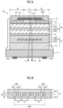
- FIG. 1A is a cross-sectional view schematically illustrating an example of a structure of a photonic-crystal laser element (PCSEL element) 10 of Example 1.
- the PCSEL element 10 is configured such that a plurality of semiconductor layers is laminated on a substrate.
- the semiconductor layer consists of a hexagonal nitride semiconductor such as a GaN-based semiconductor, for example.
- FIG. 1B is an enlarged cross-sectional view schematically illustrating a photonic crystal layer 14P in FIG. 1A and an air hole pair 14K arranged in the photonic crystal layer 14P.
- FIG. 2A is a plan view schematically illustrating an upper surface of the PCSEL element 10
- FIG. 2B is a cross-sectional view schematically illustrating a cross-section of the photonic crystal layer (PC layer) 14P on a plane parallel to the n-guide layer 14 (a cross-section taken along the line A-A in FIG. 1B )
- FIG. 2C is a plan view schematically illustrating a bottom surface of the PCSEL element 10.
- a first semiconductor layer 12, an active layer 15, and a second semiconductor layer 18 are formed by being laminated on a substrate 11.
- the first semiconductor layer 12 consists of an n-clad layer (first clad layer) 13 and an n-guide layer (first guide layer) 14.
- the n-guide layer (first guide layer) 14 consists of a lower guide layer 14A, a photonic crystal layer (an air hole layer or a PC layer) 14P, and an embedded layer 14B.
- the photonic crystal layer 14P has air holes arranged with two-dimensional periodicity within a plane parallel to the layer.
- MQW structure multiple quantum well structure
- the second semiconductor layer 18 is composed of a p-guide layer (second guide layer) 16A provided on the active layer 15, an electron blocking layer (EBL) 16B provided on the p-guide layer 16A, a p-clad layer (second clad layer) 16C provided on the electron blocking layer 16B, and a p-contact layer 17 formed on the p-clad layer 16C.
- the p-guide layer 16A, the electron blocking layer 16B, and the p-clad layer 16C constitute the p-side semiconductor layer 16.
- the p-contact layer 17 is a semiconductor layer that improves ohmic contact properties with the p-electrode, and is formed of a semiconductor layer having a smaller energy bandgap and/or a semiconductor layer having a higher impurity concentration, than the p-clad layer 16C.
- the first semiconductor layer 12 includes a semiconductor layer of a first conductive type (for example, n-type), and the second semiconductor layer 18 includes a semiconductor layer of a second conductive type (for example, p-type), which is a conductive type opposite to the first conductive type.
- a first conductive type for example, n-type
- the second semiconductor layer 18 includes a semiconductor layer of a second conductive type (for example, p-type), which is a conductive type opposite to the first conductive type.
- first conductive type is the n-type and the second conductive type which is a conductive type opposite to the first conductive type is the p-type is described, but the first conductive type and the second conductive type may be the p-type and the n-type, respectively.
- n- and p- mean “n-side” and “p-side”, respectively, and do not necessarily mean that the layer has an n-type or a p-type.
- the n guide layer means a guide layer provided closer to the n-side than the active layer, and may be an undoped layer (or an i layer).
- n-clad layer 13 may include a plurality of layers instead of a single layer, and in this case, all the layers need not be n layers (n-doped layers), and may include an undoped layer (i layer). The same applies to the second semiconductor layer 18.
- the photonic-crystal laser element may be configured to have the first semiconductor layer having the photonic crystal layer 14P, the second semiconductor layer, and the active layer (light emitting layer) interposed therebetween, in which light is emitted by current injection into the active layer.
- the photonic-crystal laser element does not need to include all of the semiconductor layers described above.
- the photonic-crystal laser element may have various semiconductor layers (for example, an air hole blocking layer, a light confinement layer, a current confinement layer, and a tunnel junction layer) for improving the element characteristics.
- an annular n-electrode (cathode) 20A (first electrode) is formed on the back surface of the substrate 11, and an antireflection film 22 is provided on the inner side of an n-electrode 20A on the back surface of the substrate 11 which is the laser light emitting surface.
- a resonance frequency adjustment film (high-refractive-index layer) 31 is provided on an upper surface of the p-contact layer 17. As illustrated in FIG. 2A , the resonance frequency adjustment film 31 has a circular (cylindrical) opening part 31C having an axis CX as the central axis, and the surface of the p-contact layer 17 is exposed from the opening part 31C. Incidentally, the opening part 31C may have an elliptic shape in a top view.
- a p-electrode 20B (second electrode) which is a transparent electrode in which the opening part 31C is embedded is formed. That is, the p-electrode 20B covers the p-contact layer 17 exposed from the opening part 31C and is connected to the p-contact layer 17 by ohmic contact.
- the p-electrode 20B is formed as a transparent conductor layer having a lower refractive index than the resonance frequency adjustment film (high-refractive-index layer) 31.
- the p-electrode 20B is formed to coat the upper surface at an end part of the resonance frequency adjustment film 31 and has a circular shape in a case of being viewed from the above along the central axis CX (top view).
- a light-reflecting film (hereinafter simply referred to as a reflective film) 32 is provided on the p-electrode 20B.
- the reflective film 32 has a similar shape to the opening part 31C and has a larger area than the opening part 31C, coaxially with the central axis CX of the opening part 31C, in a top view. That is, the reflective film 32 has a size including the opening part 31C and has a circular shape in the present Example, in a top view.
- the reflective film 32 may be provided on the p-electrode 20B which is a transparent conductor layer, and on a part of the resonance frequency adjustment film (high-refractive-index layer) 31 (that is, a part around the opening part 31C).
- the coating part of the p-electrode 20B may be formed by being interposed between the reflective film 32 and the resonance frequency adjustment film 31.
- the reflective film 32 is provided to cover at least the entire opening part 31C in a top view, and preferably has a size equal to or larger than an effective diameter (beam diameter) of the laser light.
- the reflective film 32 has a circular shape coaxial with the central axis CX and has a size equal to or larger than a Gaussian beam diameter (a diameter at which the light intensity is 1/e 2 of the peak).
- a pad electrode 23 electrically connected to the p-electrode 20B is formed on the reflective film 32.
- the pad electrode 23 is formed such that the p-electrodes 20B and the reflective film 32 are embedded. Incidentally, in FIG. 2A , the pad electrode 23 is not illustrated.
- the side surfaces of the laminated semiconductor layers (that is, the first semiconductor layer 12, the active layer 15, and the second semiconductor layer 18), and the side surface and the end part of the upper surface of the resonance frequency adjustment film 31 are coated with a protective film 21 made of an insulator such as SiO 2 .
- a protective film 21 made of an insulator such as SiO 2 .
- the protective film 21 is not hatched.
- the photonic crystal layer 14P has a double-lattice structure. That is, the air hole pair 14K (the main air hole 14K1 and the secondary air hole 14K2) is formed by being embedded in the n-guide layer 14 in a two-dimensional arrangement at square lattice point positions having a period PK in a crystal growth surface (semiconductor layer growth surface), that is, a plane parallel to the n-guide layer 14 (the cross-section of A-Ain the drawing).
- the photonic crystal layer 14P is not limited to the double-lattice structure, and may have a single lattice structure or a multiple lattice structure.
- the air hole pairs 14K are provided, for example, by being arranged periodically in a circular air hole formation region 14R.
- the n-electrode (cathode) 20A is provided as an annular electrode outside the air hole formation region 14R not to overlap the air hole formation region 14R in a case of being viewed from the direction perpendicular to the photonic crystal layer 14P (that is, in a top view).
- a region inside the n-electrode 20A is the light emission region 20L.
- the annular n-electrode 20A is formed to be coaxial with the opening part 31C and the air hole formation region 14R of the resonance frequency adjustment film 31, and a diameter DP of the air hole formation region 14R is smaller than an inner diameter DE of the n-electrode 20A (DP ⁇ DE).
- each layer of the PCSEL element 10 will be described.
- the characteristic simulation of the element described below was performed based on the following detailed configuration.
- the composition, the layer thickness, and the like of each layer of the PCSEL element 10 are merely examples, and can be modified and applied as appropriate without being particularly limited.
- the substrate 11 is a hexagonal GaN single crystal substrate having a high transmittance to light emitted from the active layer 15, and is a growth substrate. More specifically, the substrate 11 is a GaN single crystal whose main surface is a "+c" surface which is a (0001) surface having Ga atoms arranged on the outermost surface.
- the main surface may be a just substrate which is not offset, or may be, for example, a substrate which is offset by about 1° in the m-axis direction.
- a substrate which is offset by about 1° in the m-axis direction can obtain mirror growth under a wide range of growth conditions.
- a substrate surface (back surface) provided with the light emission region 20L opposite to the main surface is a "-c" surface which is a (000-1) surface where N atoms are arranged on the outermost surface.
- the -c surface is resistant to oxidation or the like, and is thus suitable as a light extraction surface.
- the GaN substrate 11 is a substrate made of an n-type GaN single crystal, and has a function as a contact layer with the n-electrode.
- the n-clad layer 13 is an n-type Al 0.04 Ga 0.96 N layer (layer thickness: 2 ⁇ m) having an Al composition of 4%.
- the carrier concentration of the n-clad layer 13 at room temperature is 1 x 10 18 cm -3 .
- the n-clad layer may have an Al composition of 2% to 10% and a thickness of 1 to 3 ⁇ m.
- the lower guide layer 14A of the n-guide layer 14 is n-type GaN and has a layer thickness of 300 nm.
- the lower guide layer 14A may have a layer thickness of, for example, 20 to 500 nm.
- the carrier concentration of the lower guide layer 14A at room temperature is 1 x 10 18 cm -3 .
- the photonic crystal layer 14P on the lower guide layer 14A includes regularly arranged air holes that resonate, in a horizontal plane, light emitted from the active layer 15.
- the photonic crystal layer 14P is an undoped GaN layer and has a layer thickness of 100 nm.
- the photonic crystal layer 14P may have a layer thickness of, for example, 60 to 150 nm.
- the air holes of the photonic crystal layer 14P will be described in detail later with reference to the drawings.
- the embedded layer 14B on the photonic crystal layer 14P is an undoped GaN layer and has a layer thickness of 100 nm.
- the embedded layer 14B may be, for example, a layer consisting of n-GaN or n-InGaN, or a layer consisting of undoped GaN or undoped InGaN, having a thickness of 50 to 150 nm.
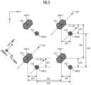
- FIG. 3 is a plan view schematically illustrating air hole pairs 14K consisting of main air holes 14K1 and secondary air holes 14K2, which are arranged at a square lattice position within a plane of the photonic crystal layer 14P, in a case of being viewed from the upper surface. That is, the photonic crystal layer 14P has a double-lattice structure. Incidentally, for the sake of clarity in the drawing, the main air holes 14K1 and the secondary air holes 14K2 are hatched.
- the main air holes 14K1 are arranged at square lattice positions with a period PK in two directions (x-direction and y-direction) in which centers CD1 of gravity are orthogonal to each other.
- the centers CD2 of gravity of the secondary air holes 14K2 are arranged at square lattice positions with the period PK in the x-direction and the y-direction.
- the period PK was set to 179 nm.
- An oscillation wavelength of the present Example was about 441 nm.
- the period PK may be appropriately adjusted according to a gain wavelength emitted from the active layer.
- the main air hole 14K1 has a long hexagonal shape surrounded by the m surface which is a ⁇ 10-10 ⁇ surface in a top view (that is, in a case of being viewed from the direction perpendicular to the photonic crystal layer 14P).
- the secondary air hole 14K2 also has a shape surrounded by the m surface.
- the x-direction and the y-direction are directions inclined by 45° with respect to the major axis direction ( ⁇ 11-20> direction) and the minor axis direction ( ⁇ 1-100> direction) of the main air hole 14K1, respectively.
- the x-y coordinate is also referred to as an air hole coordinate.
- the center CD2 of gravity of the secondary air hole 14K2 is separated from the center CD1 of gravity of the main air hole 14K1 by ⁇ x in the x direction and ⁇ y in the y direction.
- ⁇ x ⁇ y was set. That is, the center CD2 of gravity of the secondary air hole 14K2 is separated from the center CD1 of gravity of the main air hole 14K1 in the ⁇ 1-100> direction.
- the distance ⁇ x between the centers of gravity in the x direction and the distance ⁇ y between the centers of gravity in the y direction were set to 82.8 nm.
- the distance ⁇ x between the centers of gravity in the x direction and the distance ⁇ y between the centers of gravity in the y direction may be appropriately adjusted according to the laser characteristics, such as a current value required for a device to which a laser element is applied and a slope efficiency of an emission intensity of the laser.
- MQW structure multiple quantum well structure
- a well layer having a two-layer quantum well structure was used.
- the active layer 15 was disposed within 180 nm from the air hole layer (photonic crystal layer 14P) with a distance at which a resonance effect by the air hole layer was sufficiently obtained.
- the p-guide layer 16A of the second semiconductor layer 18 is an undoped InGaN layer having a layer thickness of 250 nm.
- the p-guide layer 16A may have a layer thickness of 100 to 500 nm and may be an AIInGaN layer of an undoped.
- the p-guide layer 16A is an undoped layer in consideration of light absorption by the dopant, but for example, magnesium (Mg) may be doped in order to obtain satisfactory electrical conductivity.
- Mg magnesium
- An electron blocking layer (EBL) 16B provided on the p-guide layer 16A is a magnesium-doped p-type Al 0.20 Ga 0.80 N layer with a layer thickness of 15 nm and an Al composition of 20%.
- the aluminum (Al) composition of EBL16B was set to have a composition that can serve as a barrier (energy difference) capable of preventing electrons, which are carriers, from flowing into the p-clad layer 16C.
- the EBL16B may be a multilayer structure in which the Al concentration is changed, in addition to AlGaN having a constant Al concentration.
- the p-clad layer 16C has a layer thickness of 100 nm and is magnesium-doped p-type Al 0.06 Ga 0.94 N.
- the p-clad layer 16C may have an Al composition of 2% to 10% and a layer thickness of 100 to 350 nm.
- the p-contact layer 17 is provided on the p-clad layer 16C.
- the p-contact layer 17 had a layer thickness of 25 nm and was magnesium-doped p-type GaN.
- the carrier concentration of the p-contact layer 17 was set to a concentration at which the layer could be ohmically bonded to the anode electrode provided on a surface thereof.
- an InGaN layer having a layer thickness of 2 nm or less, or an Si- or O-doped p-type GaN layer having a layer thickness of 2 nm or less may be provided on the outermost surface. By adding such a layer, the contact resistance of the p-electrode can be reduced.
- the resonance frequency adjustment film (high-refractive-index layer) 31 has a higher refractive index than the p-electrode 20B which is a transparent electrode, and is formed of a transparent and insulating material with respect to the oscillation wavelength of the active layer 15.
- the resonance frequency adjustment film 31 can be formed by depositing ZrO2 using a sputtering method.
- a cylindrical (diameter of 300 ⁇ m ⁇ ) opening part 31C having the axis CX as a central axis is formed.
- the opening part 31C can be formed by a well-known method such as chemical etching or dry etching of a ZrO2 film.
- a method for forming the resonance frequency adjustment film 31 is not limited to the sputtering method, and a CVD method, an electron beam vapor deposition method, an ALD method, an ion plating method, or the like can be used.
- an insulating light-transmitting dielectric layer such as ZrO 2 , TiO 2 , Ta 2 O 5 , Nb 2 O 5 , and SiN x can be used.
- a semiconductor layer such as GaN, AlGaN, InGaN, AlInGaN, and AlN can also be used.
- the semiconductor layer is set to be of a conductive type (that is, p-type) opposite to the semiconductor layer (n-type) as an underlayer, or the semiconductor layer is set to be insulating by ion implantation or the like.
- the refractive index of the p-electrode 20B is about 2.0
- the resonance frequency adjustment film 31 the light-transmitting dielectric layer or light-transmitting semiconductor layer having a higher refractive index than the p-electrode 20B can be used.
- the light-transmitting dielectric layer or light-transmitting semiconductor layer described above may be used as a single layer, but a layer obtained by laminating a plurality of these layers can be used as the resonance frequency adjustment film 31.
- the layer may include at least one layer or a plurality of layers.
- a light-transmitting dielectric layer such as SiO 2 may be further provided on the light-transmitting dielectric layer and/or light-transmitting semiconductor layer described above.
- ITO Indium tin oxide
- the p-electrode 20B which is a transparent conductor was used as the p-electrode 20B.
- ITO can be formed by a sputtering method.
- the p-electrode 20B has a thickness of 135 nm and is formed to fill the opening part 31C.
- the ITO film is preferably crystallized and heated by a lamp heating method in a nitrogen gas atmosphere to which oxygen has been added, for the purpose of reducing contact resistance and attaining transparency.
- a transparent conductor such as ZnO or GZO (Ga-doped ZnO) can be used in addition to ITO.
- the p-electrode 20B is in ohmic contact with the p-contact layer 17.
- the thickness is preferably in a range of 50 nm to 300 nm.
- the thickness is preferably 50 nm or more in order to function as a cladding (light confinement) since in a case where the thickness is too large, the stress is large, the peeling easily occurs, and the absorption loss increases.
- the reflective film 32 has a circular shape having a diameter of 350 ⁇ m with the axis CX as a center.
- the material of the reflective film 32 a material having a high reflectivity with respect to laser light is preferable, and for example, a metal such as Ag, Al, Rh, Pd, and Pt, or an alloy based on these materials can be used.
- a dielectric DBR in which SiO 2 /Ta 2 O 5 or the like is laminated in a multi-layered manner can be used. Further, the dielectric DBR and the highly reflective metal film may be combined.
- a pad electrode 23 electrically connected to the p-electrode 20B is formed on the reflective film 32.
- the pad electrode 23 consists of Ni/Pd/Au having thicknesses of 10 nm, 200 nm, and 500 nm (Au is the outermost surface), respectively, and is formed such that the p-electrode 20B and the reflective film 32 are embedded.
- the pad electrode 23 has a rectangular shape of 700 ⁇ m x 700 ⁇ m in a top view. Furthermore, the outer shape of the PCSEL element 10 also has a rectangular columnar shape of about 800 ⁇ m x 800 ⁇ m.
- the n-electrode 20A consists of Ti/Pt/Au (Au is the outermost surface) and is in ohmic contact with the growth substrate 11.
- Ti/Al, Ti/Rh, Ti/Al/Pt/Au, Ti/Au, V/Al/Au, V/Rh/Au, V/Al/Pt/Au, V/Pt/Au, or the like can be selected in addition to Ti/Pt/Au. It is preferable that the outermost surface is Au for wire bonding of Au.
- the protective film 21 protects the crystal layer including aluminum (Al) constituting the PCSEL from a corrosive gas or the like.
- the present invention also protects against a short circuit and the like caused by the adhesion of foreign matters or the creeping of a solder at the time of mounting, and improves reliability and a yield.
- the material is not limited to SiO 2 , and ZrO 2 , HfO 2 , TiO 2 , Al 2 O 3 , or the like can be selected.
- the PCSEL element of Comparative Example has the same structure as the PCSEL element 10 of Example 1, except that the material used as the resonance frequency adjustment film 31 is different.
- Example 1 a material having a higher refractive index than the p-electrode 20B is used as the resonance frequency adjustment film 31, but in Comparative Example, SiO 2 , which is a material having a lower refractive index than the p-electrode 20B, is used.
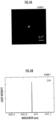
- FIGS. 4A and 4B each illustrate the calculation results of a far-field pattern (FFP) and an oscillation spectrum in a case where a constant current of 2 A (Amperes) is applied to the PCSEL element 10 of Example 1.
- FIG. 5A and FIG. 5B each illustrate the calculation results of a far-field pattern (FFP) and an oscillation spectrum in a case where a constant current of 2 A (amperes) is applied to the PCSEL element of Comparative Example.
- FIG. 6 is a view illustrating photonic bands of Example 1 (EMB1) and Comparative Example (CMP) at the time of no current injection and at the time of current injection (CW).
- a gap between the band edges BE1 and BE2 is a photonic bandgap (PBG).
- a region I central region
- a region II peripheral region
- Example 1 The far-field patterns, which are beam characteristics, at a current of 2 A in Example 1 and Comparative Example are compared with reference to FIGS. 4A and 5A .
- Example 1 a far-field pattern having a narrow spread angle was observed.
- Comparative Example cross-shaped side lobes appeared around a beam having a narrow spread angle.
- the carrier density is increased and the refractive index is decreased, as compared with the semiconductor layer in the region II which is the peripheral region.
- the band edge frequency of the region I increases occurs at the same time.
- the increase in the refractive index due to the heat generation of the CW operation greatly affects the band edge frequency, as compared with the decrease in the refractive index due to the increase in the carrier density.
- the inventors have considered that the band edge frequency of the region I was significantly decreased.
- the photonic band frequency is decreased due to the heat generation to promote the current injection, and largely deviates from the photonic band frequency of the peripheral region (region II).
- region II the photonic band frequency of the peripheral region
- Example 1 shows a longitudinal single-mode oscillation
- Comparative Example shows a longitudinal multi-mode oscillation
- a spectrum near 440.85 nm in Comparative Example corresponds to the spectrum of a beam ( FIG. 5A ) extending crosswise.
- a photonic-crystal surface-emitting laser element having high beam quality, which suppresses a higher-order mode oscillation and side lobes in the CW operation, maintains a fundamental mode until high current injection, and has stable transverse modes and longitudinal modes.
- FIG. 7 is a cross-sectional view schematically illustrating an example of a structure of a PCSEL element 40 of Example 2 (EMB2).
- the PCSEL element 40 is different from the PCSEL element 10 of Example 1 in that it has the resonance frequency adjustment film 31 having a larger thickness than the p-electrode 20B.
- the layer configuration of a semiconductor light emitting structure layer consisting of a first semiconductor layer 12, an active layer 15, and a second semiconductor layer 18 is the same as in the PCSEL element 10 of Example 1.
- the p-electrode 20B having a smaller refractive index than the resonance frequency adjustment film 31 has a smaller thickness than the resonance frequency adjustment film 31, and is formed on the p-contact layer 17.
- the p-electrode 20B is formed by being embedded in the opening part 31C by the reflective film 32.
- the p-electrode 20B which is a transparent conductor layer is provided in the opening part 31C which is a central region of the upper surface of the semiconductor light emitting structure layer, and the resonance frequency adjustment film 31 having a higher refractive index than the transparent conductor layer is provided in the peripheral region.
- the optical path length in the direction perpendicular to the semiconductor light emitting structure layer in the region of the resonance frequency adjustment film 31 is longer than that in the region I (the central region), and thus, the adjustment range can be increased. Therefore, it is possible to improve the stability of the transverse mode and the longitudinal mode at the time of the CW operation.
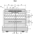
- FIG. 8 is a cross-sectional view schematically illustrating an example of a structure of a PCSEL element 50 of Example 3 (EMB3).
- the PCSEL element 50 is different from the PCSEL element 10 of Example 1 and the PCSEL element 40 of Example 2 in that it has the resonance frequency adjustment film 31 which reaches the inside of the p-clad layer 16C.
- the layer configuration of a semiconductor light emitting structure layer consisting of a first semiconductor layer 12, an active layer 15, and a second semiconductor layer 18 is the same as in the PCSEL element 10 of Example 1.
- the resonance frequency adjustment film 31 reaches the inside of the p-clad layer 16C, and a part of the p-clad layer 16C, the p-contact layer 17, and the p-electrode 20B are formed by being embedded in the opening part 31C by the reflective film 32.
- the structure of the present Example can be realized by etching the p-contact layer 17 and the p-clad layer 16C in a region excluding the central region (region I) to form the resonance frequency adjustment film 31 in the region (region II).
- the p-electrode 20B which is a transparent conductor layer is provided in the opening part 31C which is a central region of the upper surface of the semiconductor light emitting structure layer, and the resonance frequency adjustment film 31 having a higher refractive index than the transparent conductor layer is provided in the peripheral region.
- the optical path length in the direction perpendicular to the semiconductor light emitting structure layer in the region of the resonance frequency adjustment film 31 is longer than that in the region I (the central region), and thus, the adjustment range can be increased. Therefore, it is possible to improve the stability of the transverse mode and the longitudinal mode at the time of the CW operation.
- region II high-refractive-index region
- region I A region of the opening part (low-refractive-index region: region I) may have an n-gonal shape (n is an integer of 4 or more). In this case, it is preferable to have a polygonal shape of a hexagonal or higher shape (6 ⁇ n).
- the opening part (region I) of the resonance frequency adjustment film has a rotationally symmetrical shape with respect to the central axis CX.
- the opening part has a polygonal shape in a top view, it is preferable that the opening part has a regular polygonal shape.
- the opening part has a columnar shape
- the present invention is not limited thereto, and the opening part may have a truncated conical shape, a polygonal truncated pyramid shape, or the like.
- the opening part has a regular polygonal truncated pyramid shape.
- a photonic-crystal surface-emitting laser element having high beam quality, which suppresses a higher-order mode oscillation and side lobes in the CW operation, maintains a fundamental mode until high current injection, and has stable transverse modes and longitudinal modes.
Landscapes
- Physics & Mathematics (AREA)
- Condensed Matter Physics & Semiconductors (AREA)
- General Physics & Mathematics (AREA)
- Electromagnetism (AREA)
- Optics & Photonics (AREA)
- Geometry (AREA)
- Semiconductor Lasers (AREA)
Abstract
Description
- The present invention relates to a photonic-crystal surface-emitting laser element.
- In recent years, the development of a photonic-crystal surface-emitting laser using a photonic-crystal (PC) has progressed.
- For example, Non-Patent Literature 1 discloses an in-plane diffraction effect and a threshold gain difference of a photonic-crystal laser, and Non-Patent Literature 2 discloses a three-dimensional coupled wave model of a square lattice photonic-crystal laser.
- In addition, a photonic-crystal surface-emitting laser having a multiple lattice photonic crystal which is configured by disposing a plurality of air holes having different sizes at lattice points is known.
- For example, Patent Literature 1 describes a two-dimensional photonic-crystal surface-emitting laser light source having a two-dimensional photonic crystal in which a large number of different refractive index region aggregates are periodically arranged in a plate-shaped base material, in which the different refractive index region aggregate consists of a plurality of regions having different refractive indices from the refractive index of the base material, and at least two of the regions have different thicknesses from each other.
- In addition, Non-Patent Literature 3 discloses that multimode oscillation causing beam quality to be deteriorated is suppressed by changing the air hole size or the lattice constant of a photonic crystal.
- However, since the photonic crystal has very small air holes, it is difficult to accurately produce the size or the lattice constant of the air holes.
- In such a two-dimensional photonic-crystal surface-emitting laser element, it is important to realize a laser element having high beam quality, which is stable even at the time of high current injection while suppressing a higher-order mode oscillation and maintaining a fundamental mode.
- Patent Literature 1:
Japanese Patent No. 4294023 -
- Non-Patent Literature 1: Tanaka et al., Proceedings of The Japan Society of Applied Physics, Autumn Meeting 2016, 15p-B4-20
- Non-Patent Literature 2: Y. Liang et al.: Phys. Rev. B vol. 84 (2011) 195119
- Non-Patent Literature 3: M. Yoshida et al., Proceedings of the IEEE (2019). "Experimental Investigation of Lasing Modes in Double-Lattice Photonic-Crystal Resonators and Introduction of In-Plane Heterostructures."
- The present invention has been made on the basis of a finding obtained in that beam quality is deteriorated by a mechanism different from a pulse operation in a continuous oscillation operation or a continuous wave (CW) operation of a photonic-crystal surface-emitting laser element.
- An object of the present invention is to provide a photonic-crystal surface-emitting laser element having high beam quality, which suppresses a higher-order mode oscillation and side lobes in the CW operation, maintains a fundamental mode until high current injection, and has stable transverse modes and longitudinal modes.
- A surface-emitting laser element according to one embodiment of the present invention is a photonic-crystal surface-emitting laser element having a photonic crystal layer, including:
- a first semiconductor layer in which the photonic crystal layer having air holes arranged with two-dimensional periodicity within a plane parallel to the layer is formed;
- an active layer formed on the first semiconductor layer;
- a second semiconductor layer formed on the active layer;
- a high-refractive-index layer that is formed on the second semiconductor layer and has, at a central region, an opening part exposing the second semiconductor layer;
- a transparent conductor layer that covers the second semiconductor layer exposed at the opening part, is electrically connected to the second semiconductor layer, and has a lower refractive index than the high-refractive-index layer; and
- a light-reflecting film that is provided on the transparent conductor layer and the high-refractive-index layer, and reflects light incident via the opening part and the second semiconductor layer.
-
-
FIG. 1A is a cross-sectional view schematically illustrating an example of a structure of a photonic-crystal laser element (PCSEL element) 10 of Example 1. -
FIG. 1B is an enlarged cross-sectional view schematically illustrating aphotonic crystal layer 14P inFIG. 1A and anair hole pair 14K arranged in thephotonic crystal layer 14P. -
FIG. 2A is a plan view schematically illustrating an upper surface of thePCSEL element 10. -
FIG. 2B is a cross-sectional view schematically illustrating a cross-section of thephotonic crystal layer 14P on a plane parallel to the n-guide layer 14 (cross-section taken along a line A-A inFIG. 1B ). -
FIG. 2C is a plan view schematically illustrating a bottom surface of thePCSEL element 10. -
FIG. 3 is a plan view schematically illustratingair hole pairs 14K consisting of main air holes 14K1 and secondary air holes 14K2, which are arranged at a square lattice position within a plane of thephotonic crystal layer 14P. -
FIG. 4A is a view illustrating a calculation result of a far-field pattern (FFP) in a case where a constant current of 2 A is applied to thePCSEL element 10 of Example 1. -
FIG. 4B is a view illustrating a calculation result of an oscillation spectrum in a case where a constant current of 2 A is applied to thePCSEL element 10 of Example 1. -
FIG. 5A is a view illustrating a calculation result of a far-field pattern (FFP) in a case where a constant current of 2 A is applied to the PCSEL element of Comparative Example. -
FIG. 5B is a graph illustrating a calculation result of an oscillation spectrum in a case where a constant current of 2 A is applied to the PCSEL element of Comparative Example. -
FIG. 6 is a view illustrating photonic bands of Example 1 (EMB 1) and Comparative Example (CMP) at the time of no current injection and at the time of current injection (CW). -
FIG. 7 is a cross-sectional view schematically illustrating an example of a structure of aPCSEL element 40 of Example 2 (EMB2). -
FIG. 8 is a cross-sectional view schematically illustrating an example of a structure of aPCSEL element 50 of Example 3 (EMB3). - Hereinafter, preferred embodiments of the present invention will be described, but these embodiments may be appropriately modified and combined. In addition, in the following description and the accompanying drawings, substantially the same or equivalent parts will be described with the same reference numerals.
- A photonic-crystal surface-emitting laser (hereinafter also referred to as a PCSEL) is an element that has a resonator layer parallel to a semiconductor light emitting structure layer (consisting of an n-guide layer, a light emitting layer, and a p-guide layer) constituting a light emitting element, and emits coherent light in the direction orthogonal to the resonator layer.
- On the other hand, a distributed bragg reflector (DBR) laser having a pair of resonator mirrors (bragg reflectors) that interpose a semiconductor light emitting structure layer therebetween is known, but the photonic-crystal surface-emitting laser (PCSEL) differs from the DBR laser in terms of the following points. That is, in the photonic-crystal surface-emitting laser (PCSEL), a light wave propagating within a plane parallel to the photonic crystal layer is diffracted due to a diffraction effect of the photonic crystal to form a two-dimensional resonance mode, and is also diffracted in the direction perpendicular to the parallel plane. That is, a light extraction direction is a direction which is perpendicular to the resonance direction (within a plane parallel to the photonic crystal layer).
-
FIG. 1A is a cross-sectional view schematically illustrating an example of a structure of a photonic-crystal laser element (PCSEL element) 10 of Example 1. The PCSELelement 10 is configured such that a plurality of semiconductor layers is laminated on a substrate. The semiconductor layer consists of a hexagonal nitride semiconductor such as a GaN-based semiconductor, for example. - In addition,
FIG. 1B is an enlarged cross-sectional view schematically illustrating aphotonic crystal layer 14P inFIG. 1A and anair hole pair 14K arranged in thephotonic crystal layer 14P. -
FIG. 2A is a plan view schematically illustrating an upper surface of thePCSEL element 10,FIG. 2B is a cross-sectional view schematically illustrating a cross-section of the photonic crystal layer (PC layer) 14P on a plane parallel to the n-guide layer 14 (a cross-section taken along the line A-A inFIG. 1B ), andFIG. 2C is a plan view schematically illustrating a bottom surface of thePCSEL element 10. - The structure of the
PCSEL element 10 will be described in detail below with reference to the accompanying drawings. In thePCSEL element 10, afirst semiconductor layer 12, anactive layer 15, and asecond semiconductor layer 18 are formed by being laminated on asubstrate 11. - The
first semiconductor layer 12 consists of an n-clad layer (first clad layer) 13 and an n-guide layer (first guide layer) 14. In addition, the n-guide layer (first guide layer) 14 consists of alower guide layer 14A, a photonic crystal layer (an air hole layer or a PC layer) 14P, and an embeddedlayer 14B. Thephotonic crystal layer 14P has air holes arranged with two-dimensional periodicity within a plane parallel to the layer. - The
active layer 15 has a multiple quantum well structure (MQW structure) in which a GaN barrier layer and an InxGayN (x + y = 1) well layer are alternately laminated. - The
second semiconductor layer 18 is composed of a p-guide layer (second guide layer) 16A provided on theactive layer 15, an electron blocking layer (EBL) 16B provided on the p-guide layer 16A, a p-clad layer (second clad layer) 16C provided on theelectron blocking layer 16B, and a p-contact layer 17 formed on the p-cladlayer 16C. The p-guide layer 16A, theelectron blocking layer 16B, and the p-cladlayer 16C constitute the p-side semiconductor layer 16. - The p-
contact layer 17 is a semiconductor layer that improves ohmic contact properties with the p-electrode, and is formed of a semiconductor layer having a smaller energy bandgap and/or a semiconductor layer having a higher impurity concentration, than the p-cladlayer 16C. - That is, the
first semiconductor layer 12 includes a semiconductor layer of a first conductive type (for example, n-type), and thesecond semiconductor layer 18 includes a semiconductor layer of a second conductive type (for example, p-type), which is a conductive type opposite to the first conductive type. - In the present specification, a case where the first conductive type is the n-type and the second conductive type which is a conductive type opposite to the first conductive type is the p-type is described, but the first conductive type and the second conductive type may be the p-type and the n-type, respectively.
- Furthermore, in the present specification, "n-" and "p-" mean "n-side" and "p-side", respectively, and do not necessarily mean that the layer has an n-type or a p-type. For example, the n guide layer means a guide layer provided closer to the n-side than the active layer, and may be an undoped layer (or an i layer).
- In addition, the n-clad
layer 13 may include a plurality of layers instead of a single layer, and in this case, all the layers need not be n layers (n-doped layers), and may include an undoped layer (i layer). The same applies to thesecond semiconductor layer 18. - In addition, in the description above, the specific and detailed configuration of the semiconductor layer of the photonic-
crystal laser element 10 has been described, but the description is merely an example of the element structure. In brief, the photonic-crystal laser element may be configured to have the first semiconductor layer having thephotonic crystal layer 14P, the second semiconductor layer, and the active layer (light emitting layer) interposed therebetween, in which light is emitted by current injection into the active layer. - For example, the photonic-crystal laser element does not need to include all of the semiconductor layers described above. Alternatively, the photonic-crystal laser element may have various semiconductor layers (for example, an air hole blocking layer, a light confinement layer, a current confinement layer, and a tunnel junction layer) for improving the element characteristics.
- In addition, an annular n-electrode (cathode) 20A (first electrode) is formed on the back surface of the
substrate 11, and anantireflection film 22 is provided on the inner side of an n-electrode 20A on the back surface of thesubstrate 11 which is the laser light emitting surface. - A resonance frequency adjustment film (high-refractive-index layer) 31 is provided on an upper surface of the p-
contact layer 17. As illustrated inFIG. 2A , the resonancefrequency adjustment film 31 has a circular (cylindrical) openingpart 31C having an axis CX as the central axis, and the surface of the p-contact layer 17 is exposed from theopening part 31C. Incidentally, theopening part 31C may have an elliptic shape in a top view. - In the
opening part 31C, a p-electrode 20B (second electrode) which is a transparent electrode in which theopening part 31C is embedded is formed. That is, the p-electrode 20B covers the p-contact layer 17 exposed from theopening part 31C and is connected to the p-contact layer 17 by ohmic contact. - The p-
electrode 20B is formed as a transparent conductor layer having a lower refractive index than the resonance frequency adjustment film (high-refractive-index layer) 31. - In the present Example, the p-
electrode 20B is formed to coat the upper surface at an end part of the resonancefrequency adjustment film 31 and has a circular shape in a case of being viewed from the above along the central axis CX (top view). - A light-reflecting film (hereinafter simply referred to as a reflective film) 32 is provided on the p-
electrode 20B. Thereflective film 32 has a similar shape to theopening part 31C and has a larger area than theopening part 31C, coaxially with the central axis CX of theopening part 31C, in a top view. That is, thereflective film 32 has a size including theopening part 31C and has a circular shape in the present Example, in a top view. - Furthermore, the
reflective film 32 may be provided on the p-electrode 20B which is a transparent conductor layer, and on a part of the resonance frequency adjustment film (high-refractive-index layer) 31 (that is, a part around theopening part 31C). However, as illustrated inFIG. 1A , in a case where the p-electrode 20B has a coating part that coats the upper surface at an end part of the resonancefrequency adjustment film 31, the coating part of the p-electrode 20B may be formed by being interposed between thereflective film 32 and the resonancefrequency adjustment film 31. - In addition, the
reflective film 32 is provided to cover at least theentire opening part 31C in a top view, and preferably has a size equal to or larger than an effective diameter (beam diameter) of the laser light. For example, it is preferable that thereflective film 32 has a circular shape coaxial with the central axis CX and has a size equal to or larger than a Gaussian beam diameter (a diameter at which the light intensity is 1/e2 of the peak). - A
pad electrode 23 electrically connected to the p-electrode 20B is formed on thereflective film 32. Thepad electrode 23 is formed such that the p-electrodes 20B and thereflective film 32 are embedded. Incidentally, inFIG. 2A , thepad electrode 23 is not illustrated. - The side surfaces of the laminated semiconductor layers (that is, the
first semiconductor layer 12, theactive layer 15, and the second semiconductor layer 18), and the side surface and the end part of the upper surface of the resonancefrequency adjustment film 31 are coated with aprotective film 21 made of an insulator such as SiO2. Incidentally, for the sake of clarity of the drawings, theprotective film 21 is not hatched. - Light directly emitted from the
photonic crystal layer 14P (directly emitted light Ld), and light emitted from thephotonic crystal layer 14P, transmitted through the p-electrode 20B and the resonancefrequency adjustment film 31, and reflected by the reflective film 32 (reflected emitted light Lr) are emitted to the outside from alight emission region 20L on the back surface of thesubstrate 11. - As illustrated in
FIG. 1B , in the present Example, thephotonic crystal layer 14P has a double-lattice structure. That is, theair hole pair 14K (the main air hole 14K1 and the secondary air hole 14K2) is formed by being embedded in the n-guide layer 14 in a two-dimensional arrangement at square lattice point positions having a period PK in a crystal growth surface (semiconductor layer growth surface), that is, a plane parallel to the n-guide layer 14 (the cross-section of A-Ain the drawing). Incidentally, thephotonic crystal layer 14P is not limited to the double-lattice structure, and may have a single lattice structure or a multiple lattice structure. - As illustrated in
FIG. 2B , in thephotonic crystal layer 14P, the air hole pairs 14K are provided, for example, by being arranged periodically in a circular airhole formation region 14R. As illustrated inFIG. 2C , the n-electrode (cathode) 20A is provided as an annular electrode outside the airhole formation region 14R not to overlap the airhole formation region 14R in a case of being viewed from the direction perpendicular to thephotonic crystal layer 14P (that is, in a top view). A region inside the n-electrode 20A is thelight emission region 20L. - In addition, as illustrated in
FIGS. 2B and 2C , the annular n-electrode 20A is formed to be coaxial with theopening part 31C and the airhole formation region 14R of the resonancefrequency adjustment film 31, and a diameter DP of the airhole formation region 14R is smaller than an inner diameter DE of the n-electrode 20A (DP < DE). - Hereinafter, details of each layer of the
PCSEL element 10 will be described. The characteristic simulation of the element described below was performed based on the following detailed configuration. However, the composition, the layer thickness, and the like of each layer of thePCSEL element 10 are merely examples, and can be modified and applied as appropriate without being particularly limited. - The
substrate 11 is a hexagonal GaN single crystal substrate having a high transmittance to light emitted from theactive layer 15, and is a growth substrate. More specifically, thesubstrate 11 is a GaN single crystal whose main surface is a "+c" surface which is a (0001) surface having Ga atoms arranged on the outermost surface. - Furthermore, the main surface may be a just substrate which is not offset, or may be, for example, a substrate which is offset by about 1° in the m-axis direction. For example, a substrate which is offset by about 1° in the m-axis direction can obtain mirror growth under a wide range of growth conditions.
- A substrate surface (back surface) provided with the
light emission region 20L opposite to the main surface is a "-c" surface which is a (000-1) surface where N atoms are arranged on the outermost surface. The -c surface is resistant to oxidation or the like, and is thus suitable as a light extraction surface. - In the present Example, the
GaN substrate 11 is a substrate made of an n-type GaN single crystal, and has a function as a contact layer with the n-electrode. - The n-clad
layer 13 is an n-type Al0.04Ga0.96N layer (layer thickness: 2 µm) having an Al composition of 4%. In addition, the carrier concentration of the n-cladlayer 13 at room temperature is 1 x 1018 cm-3. The n-clad layer may have an Al composition of 2% to 10% and a thickness of 1 to 3 µm. - The
lower guide layer 14A of the n-guide layer 14 is n-type GaN and has a layer thickness of 300 nm. Thelower guide layer 14A may have a layer thickness of, for example, 20 to 500 nm. In addition, the carrier concentration of thelower guide layer 14A at room temperature is 1 x 1018 cm-3. - The
photonic crystal layer 14P on thelower guide layer 14A includes regularly arranged air holes that resonate, in a horizontal plane, light emitted from theactive layer 15. - The
photonic crystal layer 14P is an undoped GaN layer and has a layer thickness of 100 nm. Thephotonic crystal layer 14P may have a layer thickness of, for example, 60 to 150 nm. Incidentally, the air holes of thephotonic crystal layer 14P will be described in detail later with reference to the drawings. - The embedded
layer 14B on thephotonic crystal layer 14P is an undoped GaN layer and has a layer thickness of 100 nm. Incidentally, the embeddedlayer 14B may be, for example, a layer consisting of n-GaN or n-InGaN, or a layer consisting of undoped GaN or undoped InGaN, having a thickness of 50 to 150 nm. -
FIG. 3 is a plan view schematically illustrating air hole pairs 14K consisting of main air holes 14K1 and secondary air holes 14K2, which are arranged at a square lattice position within a plane of thephotonic crystal layer 14P, in a case of being viewed from the upper surface. That is, thephotonic crystal layer 14P has a double-lattice structure. Incidentally, for the sake of clarity in the drawing, the main air holes 14K1 and the secondary air holes 14K2 are hatched. - More specifically, the main air holes 14K1 are arranged at square lattice positions with a period PK in two directions (x-direction and y-direction) in which centers CD1 of gravity are orthogonal to each other. Similarly, the centers CD2 of gravity of the secondary air holes 14K2 are arranged at square lattice positions with the period PK in the x-direction and the y-direction. Specifically, the period PK was set to 179 nm. An oscillation wavelength of the present Example was about 441 nm. Here, the period PK may be appropriately adjusted according to a gain wavelength emitted from the active layer.
- The main air hole 14K1 has a long hexagonal shape surrounded by the m surface which is a { 10-10} surface in a top view (that is, in a case of being viewed from the direction perpendicular to the
photonic crystal layer 14P). The secondary air hole 14K2 also has a shape surrounded by the m surface. - Furthermore, the x-direction and the y-direction are directions inclined by 45° with respect to the major axis direction (<11-20> direction) and the minor axis direction (<1-100> direction) of the main air hole 14K1, respectively. In the present specification, the x-y coordinate is also referred to as an air hole coordinate.
- In addition, the center CD2 of gravity of the secondary air hole 14K2 is separated from the center CD1 of gravity of the main air hole 14K1 by Δx in the x direction and Δy in the y direction. Here, Δx = Δy was set. That is, the center CD2 of gravity of the secondary air hole 14K2 is separated from the center CD1 of gravity of the main air hole 14K1 in the <1-100> direction. Specifically, the distance Δx between the centers of gravity in the x direction and the distance Δy between the centers of gravity in the y direction were set to 82.8 nm. Here, the distance Δx between the centers of gravity in the x direction and the distance Δy between the centers of gravity in the y direction may be appropriately adjusted according to the laser characteristics, such as a current value required for a device to which a laser element is applied and a slope efficiency of an emission intensity of the laser.
- The
active layer 15 has a multiple quantum well structure (MQW structure) in which a GaN barrier layer having a thickness of 6 nm and an In0.14Ga0.86N (x + y = 1) well layer having a thickness of 4.0 nm are alternately laminated. In the present Example, a well layer having a two-layer quantum well structure was used. - The
active layer 15 was disposed within 180 nm from the air hole layer (photonic crystal layer 14P) with a distance at which a resonance effect by the air hole layer was sufficiently obtained. - The p-
guide layer 16A of thesecond semiconductor layer 18 is an undoped InGaN layer having a layer thickness of 250 nm. The p-guide layer 16A may have a layer thickness of 100 to 500 nm and may be an AIInGaN layer of an undoped. - In addition, the p-
guide layer 16A is an undoped layer in consideration of light absorption by the dopant, but for example, magnesium (Mg) may be doped in order to obtain satisfactory electrical conductivity. - An electron blocking layer (EBL) 16B provided on the p-
guide layer 16A is a magnesium-doped p-type Al0.20Ga0.80N layer with a layer thickness of 15 nm and an Al composition of 20%. - The aluminum (Al) composition of EBL16B was set to have a composition that can serve as a barrier (energy difference) capable of preventing electrons, which are carriers, from flowing into the p-clad
layer 16C. Here, the EBL16B may be a multilayer structure in which the Al concentration is changed, in addition to AlGaN having a constant Al concentration. - The p-clad
layer 16C has a layer thickness of 100 nm and is magnesium-doped p-type Al0.06Ga0.94N. The p-cladlayer 16C may have an Al composition of 2% to 10% and a layer thickness of 100 to 350 nm. - In addition, in the present Example, the p-
contact layer 17 is provided on the p-cladlayer 16C. The p-contact layer 17 had a layer thickness of 25 nm and was magnesium-doped p-type GaN. The carrier concentration of the p-contact layer 17 was set to a concentration at which the layer could be ohmically bonded to the anode electrode provided on a surface thereof. - Further, an InGaN layer having a layer thickness of 2 nm or less, or an Si- or O-doped p-type GaN layer having a layer thickness of 2 nm or less may be provided on the outermost surface. By adding such a layer, the contact resistance of the p-electrode can be reduced.
- The resonance frequency adjustment film (high-refractive-index layer) 31 has a higher refractive index than the p-
electrode 20B which is a transparent electrode, and is formed of a transparent and insulating material with respect to the oscillation wavelength of theactive layer 15. The resonancefrequency adjustment film 31 can be formed by depositing ZrO2 using a sputtering method. - In the resonance
frequency adjustment film 31, a cylindrical (diameter of 300 µmϕ) openingpart 31C having the axis CX as a central axis is formed. Theopening part 31C can be formed by a well-known method such as chemical etching or dry etching of a ZrO2 film. - Furthermore, a method for forming the resonance
frequency adjustment film 31 is not limited to the sputtering method, and a CVD method, an electron beam vapor deposition method, an ALD method, an ion plating method, or the like can be used. - In addition, as the resonance
frequency adjustment film 31, an insulating light-transmitting dielectric layer such as ZrO2, TiO2, Ta2O5, Nb2O5, and SiNx can be used. - Alternatively, a semiconductor layer such as GaN, AlGaN, InGaN, AlInGaN, and AlN can also be used. In this case, the semiconductor layer is set to be of a conductive type (that is, p-type) opposite to the semiconductor layer (n-type) as an underlayer, or the semiconductor layer is set to be insulating by ion implantation or the like.
- Furthermore, the refractive index of the p-
electrode 20B (ITO) is about 2.0, and the refractive indices of the light-transmitting dielectric layers may be shown as follows: ZrO2 (2.26), TiO2 (2.26), Ta2O5 (2.21), Nb2O5 (2.32), and SiNx (2.46) (the parentheses are the refractive indices at a wavelength λ = 440 nm). - In addition, the semiconductor layer varies depending on the composition, but the refractive index may be exemplified as follows: GaN (2.46), Al0.1Ga0.9N (2.40), In0.1Ga0.9N (2.60), and AlN (2.18) (the parentheses are the refractive indices at a wavelength λ = 440 nm).
- As described above, as the resonance
frequency adjustment film 31, the light-transmitting dielectric layer or light-transmitting semiconductor layer having a higher refractive index than the p-electrode 20B can be used. - Furthermore, the light-transmitting dielectric layer or light-transmitting semiconductor layer described above may be used as a single layer, but a layer obtained by laminating a plurality of these layers can be used as the resonance
frequency adjustment film 31. In addition, the layer may include at least one layer or a plurality of layers. - In addition, a light-transmitting dielectric layer such as SiO2 may be further provided on the light-transmitting dielectric layer and/or light-transmitting semiconductor layer described above.
- Indium tin oxide (ITO) which is a transparent conductor was used as the p-
electrode 20B. ITO can be formed by a sputtering method. In addition, the p-electrode 20B has a thickness of 135 nm and is formed to fill theopening part 31C. - Furthermore, the ITO film is preferably crystallized and heated by a lamp heating method in a nitrogen gas atmosphere to which oxygen has been added, for the purpose of reducing contact resistance and attaining transparency.
- As the p-
electrode 20B, a transparent conductor such as ZnO or GZO (Ga-doped ZnO) can be used in addition to ITO. - The p-
electrode 20B is in ohmic contact with the p-contact layer 17. The thickness is preferably in a range of 50 nm to 300 nm. The thickness is preferably 50 nm or more in order to function as a cladding (light confinement) since in a case where the thickness is too large, the stress is large, the peeling easily occurs, and the absorption loss increases. - Ag (silver) having a film thickness of 300 µm was used as the
reflective film 32 on the p-electrode 20B. Thereflective film 32 has a circular shape having a diameter of 350 µm with the axis CX as a center. - As the material of the
reflective film 32, a material having a high reflectivity with respect to laser light is preferable, and for example, a metal such as Ag, Al, Rh, Pd, and Pt, or an alloy based on these materials can be used. In addition, for example, a dielectric DBR in which SiO2/Ta2O5 or the like is laminated in a multi-layered manner can be used. Further, the dielectric DBR and the highly reflective metal film may be combined. - A
pad electrode 23 electrically connected to the p-electrode 20B is formed on thereflective film 32. Thepad electrode 23 consists of Ni/Pd/Au having thicknesses of 10 nm, 200 nm, and 500 nm (Au is the outermost surface), respectively, and is formed such that the p-electrode 20B and thereflective film 32 are embedded. - The
pad electrode 23 has a rectangular shape of 700 µm x 700 µm in a top view. Furthermore, the outer shape of thePCSEL element 10 also has a rectangular columnar shape of about 800 µm x 800 µm. - The n-
electrode 20A consists of Ti/Pt/Au (Au is the outermost surface) and is in ohmic contact with thegrowth substrate 11. As the electrode material, Ti/Al, Ti/Rh, Ti/Al/Pt/Au, Ti/Au, V/Al/Au, V/Rh/Au, V/Al/Pt/Au, V/Pt/Au, or the like can be selected in addition to Ti/Pt/Au. It is preferable that the outermost surface is Au for wire bonding of Au. - The
protective film 21 protects the crystal layer including aluminum (Al) constituting the PCSEL from a corrosive gas or the like. In addition, the present invention also protects against a short circuit and the like caused by the adhesion of foreign matters or the creeping of a solder at the time of mounting, and improves reliability and a yield. The material is not limited to SiO2, and ZrO2, HfO2, TiO2, Al2O3, or the like can be selected. - The results of the characteristic simulation of the
PCSEL element 10 of Example 1 will be described below in comparison with the PCSEL element of Comparative Example. Furthermore, the PCSEL element of Comparative Example has the same structure as thePCSEL element 10 of Example 1, except that the material used as the resonancefrequency adjustment film 31 is different. - That is, in Example 1, a material having a higher refractive index than the p-
electrode 20B is used as the resonancefrequency adjustment film 31, but in Comparative Example, SiO2, which is a material having a lower refractive index than the p-electrode 20B, is used. - In this simulation, heat generation is considered in a current injection region, a refractive index distribution corresponding to the heat generation is provided, and an effective refractive index is set. The effective refractive index adjusted by the resonance
frequency adjustment film 31 was set in a region outside the current injection region and subjected to calculation. For the heat generation, a center peak temperature was set to about 50°C. -
FIGS. 4A and 4B each illustrate the calculation results of a far-field pattern (FFP) and an oscillation spectrum in a case where a constant current of 2 A (Amperes) is applied to thePCSEL element 10 of Example 1. In addition,FIG. 5A and FIG. 5B each illustrate the calculation results of a far-field pattern (FFP) and an oscillation spectrum in a case where a constant current of 2 A (amperes) is applied to the PCSEL element of Comparative Example. - In addition,
FIG. 6 is a view illustrating photonic bands of Example 1 (EMB1) and Comparative Example (CMP) at the time of no current injection and at the time of current injection (CW). A gap between the band edges BE1 and BE2 is a photonic bandgap (PBG). Furthermore, a region I (central region) corresponds to theopening part 31C, that is, a contact part between the p-electrode 20B and the p-contact layer 17, and a region II (peripheral region) corresponds to a part where the resonancefrequency adjustment film 31 is formed. - The far-field patterns, which are beam characteristics, at a current of 2 A in Example 1 and Comparative Example are compared with reference to
FIGS. 4A and5A . In Example 1, a far-field pattern having a narrow spread angle was observed. On the other hand, in Comparative Example, cross-shaped side lobes appeared around a beam having a narrow spread angle. - As illustrated in
FIG. 6 , it is considered that this is an effect of a significant decrease in the band edge frequency in the region I, which is the current injection region, due to the heat generation of the current injection region in Comparative Example (CMP). - On the other hand, during the current injection, in the semiconductor layer corresponding to the region I which is the current injection region, the carrier density is increased and the refractive index is decreased, as compared with the semiconductor layer in the region II which is the peripheral region. As a result, a phenomenon in which the band edge frequency of the region I increases occurs at the same time. However, the increase in the refractive index due to the heat generation of the CW operation greatly affects the band edge frequency, as compared with the decrease in the refractive index due to the increase in the carrier density. As a result, the inventors have considered that the band edge frequency of the region I was significantly decreased.
- More specifically, in Comparative Example, since an SiO2 film having a lower refractive index than ITO is formed on the periphery, the photonic band of the current injection region or the central region (region I) is in a state of being decreased from the time of current non-injection.
- In addition, at the time of current injection, the photonic band frequency is decreased due to the heat generation to promote the current injection, and largely deviates from the photonic band frequency of the peripheral region (region II). With a positional relationship of this photonic band, it is considered that the in-plane light confinement is significantly weakened, a threshold gain of a mode in which a narrow spread angle oscillates increases, and a mode in which the angle oscillates in a cross shape appears.
- On the other hand, in a case of Examples, due to the appropriate photonic band frequency relationship, it is considered that single-mode oscillation can be achieved without deteriorating the threshold gain of a beam with a narrow spread angle.
- With reference to the oscillation spectra of Example 1 and Comparative Example, each illustrated in
FIGS. 4B and5B , it can be seen that Example 1 shows a longitudinal single-mode oscillation, whereas Comparative Example shows a longitudinal multi-mode oscillation. Furthermore, a spectrum near 440.85 nm in Comparative Example corresponds to the spectrum of a beam (FIG. 5A ) extending crosswise. - Therefore, it is possible to provide a photonic-crystal surface-emitting laser element having high beam quality, which suppresses a higher-order mode oscillation and side lobes in the CW operation, maintains a fundamental mode until high current injection, and has stable transverse modes and longitudinal modes.
-
FIG. 7 is a cross-sectional view schematically illustrating an example of a structure of aPCSEL element 40 of Example 2 (EMB2). - The
PCSEL element 40 is different from thePCSEL element 10 of Example 1 in that it has the resonancefrequency adjustment film 31 having a larger thickness than the p-electrode 20B. The layer configuration of a semiconductor light emitting structure layer consisting of afirst semiconductor layer 12, anactive layer 15, and asecond semiconductor layer 18 is the same as in thePCSEL element 10 of Example 1. - More specifically, the p-
electrode 20B having a smaller refractive index than the resonancefrequency adjustment film 31 has a smaller thickness than the resonancefrequency adjustment film 31, and is formed on the p-contact layer 17. In addition, the p-electrode 20B is formed by being embedded in theopening part 31C by thereflective film 32. - In other words, also in the present Example, the p-
electrode 20B which is a transparent conductor layer is provided in theopening part 31C which is a central region of the upper surface of the semiconductor light emitting structure layer, and the resonancefrequency adjustment film 31 having a higher refractive index than the transparent conductor layer is provided in the peripheral region. - According to the
PCSEL element 40 of Example 2, the optical path length in the direction perpendicular to the semiconductor light emitting structure layer in the region of the resonance frequency adjustment film 31 (the region II or the peripheral region) is longer than that in the region I (the central region), and thus, the adjustment range can be increased. Therefore, it is possible to improve the stability of the transverse mode and the longitudinal mode at the time of the CW operation. -
FIG. 8 is a cross-sectional view schematically illustrating an example of a structure of aPCSEL element 50 of Example 3 (EMB3). - The
PCSEL element 50 is different from thePCSEL element 10 of Example 1 and thePCSEL element 40 of Example 2 in that it has the resonancefrequency adjustment film 31 which reaches the inside of the p-cladlayer 16C. The layer configuration of a semiconductor light emitting structure layer consisting of afirst semiconductor layer 12, anactive layer 15, and asecond semiconductor layer 18 is the same as in thePCSEL element 10 of Example 1. - More specifically, the resonance
frequency adjustment film 31 reaches the inside of the p-cladlayer 16C, and a part of the p-cladlayer 16C, the p-contact layer 17, and the p-electrode 20B are formed by being embedded in theopening part 31C by thereflective film 32. - Furthermore, the structure of the present Example can be realized by etching the p-
contact layer 17 and the p-cladlayer 16C in a region excluding the central region (region I) to form the resonancefrequency adjustment film 31 in the region (region II). - In other words, also in the present Example, the p-
electrode 20B which is a transparent conductor layer is provided in theopening part 31C which is a central region of the upper surface of the semiconductor light emitting structure layer, and the resonancefrequency adjustment film 31 having a higher refractive index than the transparent conductor layer is provided in the peripheral region. - According to the
PCSEL element 50 of Example 3, the optical path length in the direction perpendicular to the semiconductor light emitting structure layer in the region of the resonance frequency adjustment film 31 (the region II or the peripheral region) is longer than that in the region I (the central region), and thus, the adjustment range can be increased. Therefore, it is possible to improve the stability of the transverse mode and the longitudinal mode at the time of the CW operation. - Furthermore, in Examples described above, a case where the resonance frequency adjustment film (region II: high-refractive-index region) having an opening part with a circular shape (including an elliptical shape) in a top view is formed has been described as an example, but the present invention is not limited thereto. A region of the opening part (low-refractive-index region: region I) may have an n-gonal shape (n is an integer of 4 or more). In this case, it is preferable to have a polygonal shape of a hexagonal or higher shape (6 ≤ n).
- In addition, it is preferable that the opening part (region I) of the resonance frequency adjustment film has a rotationally symmetrical shape with respect to the central axis CX. For example, in a case where the opening part has a polygonal shape in a top view, it is preferable that the opening part has a regular polygonal shape.
- Moreover, a case where the opening part has a columnar shape has been described as an example, but the present invention is not limited thereto, and the opening part may have a truncated conical shape, a polygonal truncated pyramid shape, or the like. In addition, in a case of having a polygonal truncated pyramid shape, it is preferable that the opening part has a regular polygonal truncated pyramid shape.
- As described above in detail, according to the present invention, it is possible to provide a photonic-crystal surface-emitting laser element having high beam quality, which suppresses a higher-order mode oscillation and side lobes in the CW operation, maintains a fundamental mode until high current injection, and has stable transverse modes and longitudinal modes.
-
- 10, 40, 50: PCSEL element
- 11: substrate
- 12: first semiconductor layer
- 13: first clad layer
- 14: first guide layer
- 14A: lower guide layer
- 14P: photonic crystal layer
- 14B: embedded layer
- 15: active layer
- 16A: second guide layer
- 16B: electron blocking layer
- 16C: second clad layer
- 17: contact layer
- 18: second semiconductor layer
- 20A: first electrode
- 20B: light-transmitting electrode (second electrode)
- 20L: light emission region
- 21: protective film
- 23: pad electrode
- 31C: opening part
- 31: resonance frequency adjustment film (high-refractive-index layer)
Claims (7)
- A photonic-crystal surface-emitting laser element having a photonic crystal layer, comprising:a first semiconductor layer in which the photonic crystal layer having air holes arranged with two-dimensional periodicity within a plane parallel to the layer is formed;an active layer formed on the first semiconductor layer;a second semiconductor layer formed on the active layer;a high-refractive-index layer that is formed on the second semiconductor layer and has, at a central region, an opening part exposing the second semiconductor layer;a transparent conductor layer that covers the second semiconductor layer exposed at the opening part, is electrically connected to the second semiconductor layer, and has a lower refractive index than the high-refractive-index layer; anda light-reflecting film that is provided on the transparent conductor layer and the high-refractive-index layer, and reflects light incident via the opening part and the second semiconductor layer.
- The photonic-crystal surface-emitting laser element according to claim 1,wherein the transparent conductor layer fills the opening part, andthe light-reflecting film has a similar shape to the opening part and has a larger area than the opening part, coaxially with the opening part, in a case of being viewed from a direction perpendicular to the photonic crystal layer.
- The photonic-crystal surface-emitting laser element according to claim 1,wherein the high-refractive-index layer has a larger layer thickness than the transparent conductor layer,the transparent conductor layer is embedded in the opening part by the light-reflecting film, andthe light-reflecting film has a similar shape to the opening part and has a larger area than the opening part in a case of being viewed from a direction perpendicular to the photonic crystal layer, coaxially with the opening part.
- The photonic-crystal surface-emitting laser element according to claim 1,wherein the high-refractive-index layer is formed at a depth reaching an inside of the second semiconductor layer from a surface side of the second semiconductor layer,a part of the surface side of the second semiconductor layer is embedded in the opening part of the high-refractive-index layer by the transparent conductor layer, andthe light-reflecting film has a similar shape to the opening part and has a larger area than the opening part in a case of being viewed from a direction perpendicular to the photonic crystal layer, coaxially with the opening part.
- The photonic-crystal surface-emitting laser element according to any one of claims 1 to 4,
wherein the opening part has a circular shape in a case of being viewed from a direction perpendicular to the photonic crystal layer. - The photonic-crystal surface-emitting laser element according to any one of claims 1 to 5,
wherein the high-refractive-index layer includes at least one layer of a ZrO2 layer, a TiO2 layer, a Ta2O5 layer, an Nb2O5 layer, or an SiNx layer, which are insulating light-transmitting dielectric layers. - The photonic-crystal surface-emitting laser element according to any one of claims 1 to 5,wherein the high-refractive-index layer includes at least one semiconductor layer of a GaN layer, an AlGaN layer, an InGaN layer, an AlInGaN layer, or an AlN layer, andthe at least one semiconductor layer is insulating or of a conductive type opposite to the second semiconductor layer.
Applications Claiming Priority (2)
| Application Number | Priority Date | Filing Date | Title |
|---|---|---|---|
| JP2022015936A JP7831760B2 (en) | 2022-02-03 | 2022-02-03 | Photonic crystal surface-emitting laser element |
| PCT/JP2023/003460 WO2023149520A1 (en) | 2022-02-03 | 2023-02-02 | Photonic-crystal surface-light-emitting laser element |
Publications (2)
| Publication Number | Publication Date |
|---|---|
| EP4456345A1 true EP4456345A1 (en) | 2024-10-30 |
| EP4456345A4 EP4456345A4 (en) | 2025-05-07 |
Family
ID=87552581
Family Applications (1)
| Application Number | Title | Priority Date | Filing Date |
|---|---|---|---|
| EP23749836.5A Pending EP4456345A4 (en) | 2022-02-03 | 2023-02-02 | PHOTONIC CRYSTAL SURFACE LIGHT-EMITTING LASER ELEMENT |
Country Status (6)
| Country | Link |
|---|---|
| US (1) | US20250385486A1 (en) |
| EP (1) | EP4456345A4 (en) |
| JP (1) | JP7831760B2 (en) |
| KR (1) | KR20240142450A (en) |
| CN (1) | CN118749165A (en) |
| WO (1) | WO2023149520A1 (en) |
Families Citing this family (3)
| Publication number | Priority date | Publication date | Assignee | Title |
|---|---|---|---|---|
| JP7845981B2 (en) * | 2022-10-03 | 2026-04-14 | 株式会社東芝 | Surface-emitting quantum cascade laser and its control method |
| CN122122770A (en) * | 2023-11-10 | 2026-05-29 | 国立大学法人京都大学 | Two-dimensional photonic crystal surface emitting laser |
| CN121035771B (en) * | 2025-10-28 | 2026-02-27 | 苏州实验室 | A diffraction-type surface-emitting semiconductor laser |
Family Cites Families (10)
| Publication number | Priority date | Publication date | Assignee | Title |
|---|---|---|---|---|
| JP2003273456A (en) * | 2002-03-14 | 2003-09-26 | Japan Science & Technology Corp | Two-dimensional photonic crystal surface emitting laser |
| JP4294023B2 (en) | 2005-12-27 | 2009-07-08 | 国立大学法人京都大学 | Two-dimensional photonic crystal surface emitting laser light source |
| JP4975130B2 (en) * | 2009-05-07 | 2012-07-11 | キヤノン株式会社 | Photonic crystal surface emitting laser |
| JP5704901B2 (en) * | 2010-11-17 | 2015-04-22 | キヤノン株式会社 | Two-dimensional photonic crystal surface emitting laser |
| JP5769483B2 (en) * | 2011-04-21 | 2015-08-26 | キヤノン株式会社 | Surface emitting laser and image forming apparatus |
| JP7125327B2 (en) * | 2018-10-25 | 2022-08-24 | 浜松ホトニクス株式会社 | Light-emitting element and light-emitting device |
| JP7306675B2 (en) * | 2019-02-22 | 2023-07-11 | 国立大学法人京都大学 | Two-dimensional photonic crystal surface emitting laser |
| TWM611530U (en) * | 2020-04-29 | 2021-05-11 | 富昱晶雷射科技股份有限公司 | Flip-chip electrically pumped photonic crystal surface-emitting type laser element |
| JP7485284B2 (en) * | 2020-07-14 | 2024-05-16 | 国立大学法人京都大学 | Photonic crystal surface emitting laser element |
| JP7852860B2 (en) * | 2022-05-25 | 2026-04-28 | 国立大学法人京都大学 | Method for manufacturing a surface-emitting laser element |
-
2022
- 2022-02-03 JP JP2022015936A patent/JP7831760B2/en active Active
-
2023
- 2023-02-02 KR KR1020247026047A patent/KR20240142450A/en active Pending
- 2023-02-02 CN CN202380017969.7A patent/CN118749165A/en active Pending
- 2023-02-02 WO PCT/JP2023/003460 patent/WO2023149520A1/en not_active Ceased
- 2023-02-02 EP EP23749836.5A patent/EP4456345A4/en active Pending
- 2023-02-02 US US18/833,588 patent/US20250385486A1/en active Pending
Also Published As
| Publication number | Publication date |
|---|---|
| EP4456345A4 (en) | 2025-05-07 |
| JP7831760B2 (en) | 2026-03-17 |
| WO2023149520A1 (en) | 2023-08-10 |
| KR20240142450A (en) | 2024-09-30 |
| JP2023113507A (en) | 2023-08-16 |
| CN118749165A (en) | 2024-10-08 |
| US20250385486A1 (en) | 2025-12-18 |
Similar Documents
| Publication | Publication Date | Title |
|---|---|---|
| US20250385486A1 (en) | Photonic-crystal surface-light-emitting laser element | |
| JP5368957B2 (en) | Manufacturing method of semiconductor laser chip | |
| US10892601B2 (en) | Vertical cavity light-emitting element | |
| WO2022014343A1 (en) | Photonic crystal surface light-emitting laser element | |
| EP2416460B1 (en) | Nitride semiconductor laser element and method for manufacturing same | |
| EP4283804B1 (en) | Method of manufacturing a photonic crystal surface-emitting laser element | |
| US10404038B2 (en) | Quantum cascade laser | |
| US12266906B2 (en) | Vertical cavity surface emitting device | |
| JP2012505541A (en) | Vertical cavity surface emitting laser with improved mode selectivity | |
| EP4481963A1 (en) | Surface-emitting laser element | |
| US20250055259A1 (en) | Surface-emitting laser element | |
| US12407146B2 (en) | Vertical cavity light-emitting element and manufacturing method of the same | |
| JP7581248B2 (en) | Vertical cavity light emitting device | |
| US10476237B2 (en) | Quantum cascade laser | |
| US10476235B2 (en) | Quantum cascade laser | |
| WO2022049996A1 (en) | Semiconductor laser and semiconductor laser device | |
| TWI911638B (en) | Surface-emitting laser element | |
| US20250364784A1 (en) | Surface-emitting laser element | |
| JP2025119626A (en) | Photonic crystal surface-emitting laser element and photonic crystal surface-emitting laser device | |
| JP2023127163A (en) | Vertical cavity light emitting device |
Legal Events
| Date | Code | Title | Description |
|---|---|---|---|
| STAA | Information on the status of an ep patent application or granted ep patent |
Free format text: STATUS: THE INTERNATIONAL PUBLICATION HAS BEEN MADE |
|
| PUAI | Public reference made under article 153(3) epc to a published international application that has entered the european phase |
Free format text: ORIGINAL CODE: 0009012 |
|
| STAA | Information on the status of an ep patent application or granted ep patent |
Free format text: STATUS: REQUEST FOR EXAMINATION WAS MADE |
|
| 17P | Request for examination filed |
Effective date: 20240724 |
|
| AK | Designated contracting states |
Kind code of ref document: A1 Designated state(s): AL AT BE BG CH CY CZ DE DK EE ES FI FR GB GR HR HU IE IS IT LI LT LU LV MC ME MK MT NL NO PL PT RO RS SE SI SK SM TR |
|
| STAA | Information on the status of an ep patent application or granted ep patent |
Free format text: STATUS: EXAMINATION IS IN PROGRESS |
|
| A4 | Supplementary search report drawn up and despatched |
Effective date: 20250407 |
|
| DAV | Request for validation of the european patent (deleted) | ||
| DAX | Request for extension of the european patent (deleted) | ||
| RIC1 | Information provided on ipc code assigned before grant |
Ipc: H01S 5/187 20060101ALI20250401BHEP Ipc: H01S 5/11 20210101AFI20250401BHEP |
|
| 17Q | First examination report despatched |
Effective date: 20250423 |