EP4451827A1 - Display device and method for manufacturing same - Google Patents
Display device and method for manufacturing same Download PDFInfo
- Publication number
- EP4451827A1 EP4451827A1 EP22908007.2A EP22908007A EP4451827A1 EP 4451827 A1 EP4451827 A1 EP 4451827A1 EP 22908007 A EP22908007 A EP 22908007A EP 4451827 A1 EP4451827 A1 EP 4451827A1
- Authority
- EP
- European Patent Office
- Prior art keywords
- layer
- opening
- color filter
- refractive index
- low
- Prior art date
- Legal status (The legal status is an assumption and is not a legal conclusion. Google has not performed a legal analysis and makes no representation as to the accuracy of the status listed.)
- Pending
Links
Images





Classifications
-
- H—ELECTRICITY
- H10—SEMICONDUCTOR DEVICES; ELECTRIC SOLID-STATE DEVICES NOT OTHERWISE PROVIDED FOR
- H10K—ORGANIC ELECTRIC SOLID-STATE DEVICES
- H10K59/00—Integrated devices, or assemblies of multiple devices, comprising at least one organic light-emitting element covered by group H10K50/00
- H10K59/30—Devices specially adapted for multicolour light emission
- H10K59/38—Devices specially adapted for multicolour light emission comprising colour filters or colour changing media [CCM]
-
- H—ELECTRICITY
- H10—SEMICONDUCTOR DEVICES; ELECTRIC SOLID-STATE DEVICES NOT OTHERWISE PROVIDED FOR
- H10K—ORGANIC ELECTRIC SOLID-STATE DEVICES
- H10K50/00—Organic light-emitting devices
- H10K50/10—OLEDs or polymer light-emitting diodes [PLED]
- H10K50/11—OLEDs or polymer light-emitting diodes [PLED] characterised by the electroluminescent [EL] layers
- H10K50/115—OLEDs or polymer light-emitting diodes [PLED] characterised by the electroluminescent [EL] layers comprising active inorganic nanostructures, e.g. luminescent quantum dots
-
- H—ELECTRICITY
- H10—SEMICONDUCTOR DEVICES; ELECTRIC SOLID-STATE DEVICES NOT OTHERWISE PROVIDED FOR
- H10K—ORGANIC ELECTRIC SOLID-STATE DEVICES
- H10K50/00—Organic light-emitting devices
- H10K50/80—Constructional details
- H10K50/84—Passivation; Containers; Encapsulations
- H10K50/841—Self-supporting sealing arrangements
-
- H—ELECTRICITY
- H10—SEMICONDUCTOR DEVICES; ELECTRIC SOLID-STATE DEVICES NOT OTHERWISE PROVIDED FOR
- H10K—ORGANIC ELECTRIC SOLID-STATE DEVICES
- H10K50/00—Organic light-emitting devices
- H10K50/80—Constructional details
- H10K50/84—Passivation; Containers; Encapsulations
- H10K50/844—Encapsulations
-
- H—ELECTRICITY
- H10—SEMICONDUCTOR DEVICES; ELECTRIC SOLID-STATE DEVICES NOT OTHERWISE PROVIDED FOR
- H10K—ORGANIC ELECTRIC SOLID-STATE DEVICES
- H10K50/00—Organic light-emitting devices
- H10K50/80—Constructional details
- H10K50/85—Arrangements for extracting light from the devices
- H10K50/858—Arrangements for extracting light from the devices comprising refractive means, e.g. lenses
-
- H—ELECTRICITY
- H10—SEMICONDUCTOR DEVICES; ELECTRIC SOLID-STATE DEVICES NOT OTHERWISE PROVIDED FOR
- H10K—ORGANIC ELECTRIC SOLID-STATE DEVICES
- H10K59/00—Integrated devices, or assemblies of multiple devices, comprising at least one organic light-emitting element covered by group H10K50/00
- H10K59/10—OLED displays
- H10K59/12—Active-matrix OLED [AMOLED] displays
-
- H—ELECTRICITY
- H10—SEMICONDUCTOR DEVICES; ELECTRIC SOLID-STATE DEVICES NOT OTHERWISE PROVIDED FOR
- H10K—ORGANIC ELECTRIC SOLID-STATE DEVICES
- H10K71/00—Manufacture or treatment specially adapted for the organic devices covered by this subclass
-
- H—ELECTRICITY
- H10—SEMICONDUCTOR DEVICES; ELECTRIC SOLID-STATE DEVICES NOT OTHERWISE PROVIDED FOR
- H10K—ORGANIC ELECTRIC SOLID-STATE DEVICES
- H10K59/00—Integrated devices, or assemblies of multiple devices, comprising at least one organic light-emitting element covered by group H10K50/00
- H10K59/10—OLED displays
- H10K59/12—Active-matrix OLED [AMOLED] displays
- H10K59/1201—Manufacture or treatment
-
- H—ELECTRICITY
- H10—SEMICONDUCTOR DEVICES; ELECTRIC SOLID-STATE DEVICES NOT OTHERWISE PROVIDED FOR
- H10K—ORGANIC ELECTRIC SOLID-STATE DEVICES
- H10K59/00—Integrated devices, or assemblies of multiple devices, comprising at least one organic light-emitting element covered by group H10K50/00
- H10K59/80—Constructional details
- H10K59/87—Passivation; Containers; Encapsulations
- H10K59/873—Encapsulations
-
- H—ELECTRICITY
- H10—SEMICONDUCTOR DEVICES; ELECTRIC SOLID-STATE DEVICES NOT OTHERWISE PROVIDED FOR
- H10K—ORGANIC ELECTRIC SOLID-STATE DEVICES
- H10K59/00—Integrated devices, or assemblies of multiple devices, comprising at least one organic light-emitting element covered by group H10K50/00
- H10K59/80—Constructional details
- H10K59/875—Arrangements for extracting light from the devices
- H10K59/879—Arrangements for extracting light from the devices comprising refractive means, e.g. lenses
Definitions
- the disclosure relates to a display device and a manufacturing method thereof.
- a display device is a device for displaying an image. Examples may include a liquid crystal display (LCD), an organic light emitting diode (OLED) display, and the like.
- LCD liquid crystal display
- OLED organic light emitting diode
- a display device may be used in various electronic devices such as a mobile phone, a navigation device, a digital camera, an electronic book, a portable game machine, and various terminals.
- An organic light emitting device may include two electrodes and an organic emission layer positioned between the two electrodes, and electrons injected from one electrode and holes injected from another electrode may be combined on the organic emission layer to generate excitons. In case that the excitons change to a ground state from an excited state, the excitons output energy and emit light.
- the color converting panel may include semiconductor nanocrystals such as quantum dots, and may convert incident light into different colors.
- the color converting panel may further include scatterers.
- the organic light emitting device may be formed by combining the display panel on which light-emitting devices may be formed and the color converting panel. As parts may be respectively formed on two substrates, and they may be bonded to each other to realize the display device, the display device may become thick, an optical loss may be generated, and a manufacturing cost may increase.
- the described technology has been made in an effort to provide a display device for reducing a thickness, an optical loss, and a manufacturing cost of a display device, and a manufacturing method thereof.
- the described technology has been made in another effort to provide a display device for planarizing an upper side of a display device and preventing generation of diffused reflection on a surface, and a manufacturing method thereof.
- An embodiment provides a display device that may include a substrate, a transistor disposed on the substrate, a light-emitting device electrically connected to the transistor, an encapsulation layer disposed on the light-emitting device, a partition wall disposed on the encapsulation layer and including an opening overlapping the light-emitting device, and a color converting layer, a low-refractive index layer, and a color filter sequentially stacked on each other in the opening.
- the partition wall may include a first opening overlapping a light-emitting device of a first pixel, a second opening overlapping a light-emitting device of a second pixel, and a third opening overlapping a light-emitting device of a third pixel.
- a first color converting layer, the low-refractive index layer, and a first color filter may be disposed in the first opening, a second color converting layer, the low-refractive index layer, and a second color filter may be disposed in the second opening, and a transmission layer, the low-refractive index layer, and a third color filter may be disposed in the third opening.
- the low-refractive index layer may be disposed on the first color converting layer, the second color converting layer, and the transmission layer, and the low-refractive index layer may be disposed on a lateral side of the partition wall.
- the low-refractive index layer may not be disposed on an upper side (which may refer to an upper surface herein) of the partition wall.
- the first color filter, the second color filter, and the third color filter may not overlap each other.
- the first color filter, the second color filter, and the third color filter may not be disposed on an upper side of the partition wall.
- the display device may further include a first capping layer and a second capping layer that are disposed in the first opening, the second opening, and the third opening.
- the first capping layer may be disposed between the first color converting layer and the low-refractive index layer, between the second color converting layer and the low-refractive index layer, and between the transmission layer and the low-refractive index layer
- the second capping layer may be disposed between the low-refractive index layer and the first color filter, between the low-refractive index layer and the second color filter, and between the low-refractive index layer and the third color filter.
- the first capping layer and the second capping layer may be disposed on an upper side of the partition wall.
- the display device may further include an overcoat layer disposed on the first color filter, the second color filter, the third color filter, and the partition wall.
- the method may include forming a transistor and a light-emitting device electrically connected to the transistor on a substrate, forming an encapsulation layer on the light-emitting device, forming a layer for forming a partition wall on the encapsulation layer, forming an opening overlapping the light-emitting device by patterning the layer for forming the partition wall, forming a color converting layer in the opening, forming a low-refractive index layer in the opening, and forming a color filter in the opening.
- the forming of the color converting layer, the forming of the low-refractive index layer, and the forming of the color filter may be performed by using an inkjet printing process.
- the patterning of the layer for forming the partition wall may include forming a first opening overlapping a light-emitting device of a first pixel, a second opening overlapping a light-emitting device of a second pixel, and a third opening overlapping a light-emitting device of a third pixel.
- the forming of the color converting layer may include by dropping different ink materials into the first opening, the second opening, and the third opening, forming a first color converting layer in the first opening, forming a second color converting layer in the second opening, and forming a transmission layer in the third opening.
- the forming of the low-refractive index layer may include by dropping a same ink material into the first opening, the second opening, and the third opening, forming a low-refractive index layer on the first color converting layer, the second color converting layer, and the transmission layer.
- the low-refractive index layer may be disposed on a lateral side of the partition wall, and the low-refractive index layer may not be disposed on an upper side of the partition wall.
- the forming of the color filter may include by dropping different ink materials in the first opening, the second opening, and the third opening, forming a first color filter in the first opening, forming a second color filter in the second opening, and forming a third color filter in the third opening.
- the first color filter, the second color filter, and the third color filter may be disposed on the low-refractive index layer.
- the first color filter, the second color filter, and the third color filter may not overlap each other, and the first color filter, the second color filter, and the third color filter may not be disposed on an upper side of the partition wall.
- the method may further include, before the forming of the low-refractive index layer, forming a first capping layer on the first color converting layer, the second color converting layer, and the transmission layer, and after the forming of the low-refractive index layer, forming a second capping layer on the low-refractive index layer.
- the method may further include forming an overcoat layer on the first color filter, the second color filter, the third color filter, and the partition wall.
- parts such as the light-emitting devices and the color converting layers may be formed on one substrate, thereby reducing the thickness of the display device, the optical loss, and the manufacturing cost.
- the upper side of the display device may be planarized, thereby preventing generation of the diffused reflection on the surface.
- the phrase “at least one of” is intended to include the meaning of "at least one selected from the group of” for the purpose of its meaning and interpretation.
- at least one of A and B may be understood to mean “A, B, or A and B.”
- the term “and/or” is intended to include any combination of the terms “and” and “or” for the purpose of its meaning and interpretation.
- a and/or B may be understood to mean “A, B, or A and B.”
- the terms “and” and “or” may be used in the conjunctive or disjunctive sense and may be understood to be equivalent to "and/or.”
- connection to or “coupled to” may include a physical or electrical connection or coupling.
- overlap or “overlapped” mean that a first object may be above or below or to a side of a second object, and vice versa. Additionally, the term “overlap” may include layer, stack, face or facing, extending over, covering, or partly covering or any other suitable term as would be appreciated and understood by those of ordinary skill in the art.
- the phrase "in a plan view” means viewing an object portion from a position, e.g., viewing from a top position.
- the phrase "in a cross-sectional view” means viewing a cross-section of which the object portion is cut from a position, e.g., viewing a vertically cut view from a side.
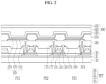
- a display device according to an embodiment will now be described with reference to FIG. 1 .
- FIG. 1 schematically shows a cross-sectional view of a display device according to an embodiment.
- the display device may include a substrate 110, a transistor TFT positioned (disposed) on the substrate 110, and a light-emitting device ED connected to the transistor TFT.
- the substrate 110 may include at least one of polystyrene, polyvinyl alcohol, polymethyl methacrylate, polyethersulfone, polyacrylate, polyetherimide, polyethylene naphthalate, polyethylene terephthalate, polyphenylene sulfide, polyarylate, polyimide, polycarbonate, triacetate cellulose, and cellulose acetate propionate.
- the substrate 110 may be a rigid substrate or a flexible substrate that may be bent, folded, or rolled.
- the substrate 110 may be a single layer or a multilayer.
- the substrate 110 may be made by alternately stacking at least one base layer including sequentially stacked polymer resins and at least one organic layer.
- a surface of the substrate 110 may be made flat.
- a buffer layer 111 may include an inorganic insulating material such as a silicon nitride (SiN x ), a silicon oxide (SiO x ), and/or a silicon oxynitride (SiO x N y ), and/or an organic insulating material.
- the buffer layer 111 may have a single-layered or multi-layered structure of the material.
- a barrier layer (not shown) may be further positioned on the substrate 110. The barrier layer may be positioned between the substrate 110 and the buffer layer 111.
- the barrier layer may include an inorganic insulating material such as a silicon nitride (SiN x ), a silicon oxide (SiO x ), and/or a silicon oxynitride (SiO x N y ).
- the barrier layer may have a single-layered or multi-layered structure of the material.
- a light blocking layer 177 may be positioned on the buffer layer 111.
- the light blocking layer 177 may block light input to a semiconductor 131.
- the light blocking layer 177 may overlap the semiconductor 131, and may have a greater width than the semiconductor 131.
- An insulating layer 113 may be positioned on the light blocking layer 177.
- the insulating layer 113 may include an inorganic insulating material such as a silicon nitride (SiN x ), a silicon oxide (SiO x ), and/or a silicon oxynitride (SiO x N y ), and/or an organic insulating material.
- the insulating layer 113 may improve a characteristic of the semiconductor 131 by blocking an inflow of impurities to the semiconductor 131 from the substrate 110.
- the semiconductor 131 may be positioned on the insulating layer 113.
- the semiconductor 131 may include at least one of amorphous silicon, polycrystalline silicon, and an oxide semiconductor.
- the semiconductor 131 may include a low temperature polysilicon (LTPS) and/or an oxide semiconductor material including at least one of zinc (Zn), indium (In), gallium (Ga), tin (Sn), or a combination thereof.
- the semiconductor 131 may include an indium-gallium-zinc oxide (IGZO).
- the semiconductor 131 may include a channel region, a source region, and a drain region distinguished by whether impurities may be doped. The source region and the drain region may have a conductive characteristic that corresponds to a conductor.
- a gate insulating layer 120 may be positioned on the semiconductor 131.
- the gate insulating layer 120 may have a single-layered or multi-layered structure.
- the gate insulating layer 120 may include an inorganic insulating material such as a silicon nitride (SiN x ), a silicon oxide (SiO x ), and/or a silicon oxynitride (SiO x N y ).
- the gate insulating layer 120 may cover at least part of the semiconductor 131.
- the gate insulating layer 120 may overlap the channel region of the semiconductor 131.
- the gate insulating layer 120 may not overlap the source region and the drain region of the semiconductor 131.
- the gate insulating layer 120 may generally cover the semiconductor 131.
- the gate insulating layer 120 may be generally positioned on the substrate 110.
- a gate electrode 124 may be positioned on the gate insulating layer 120.
- the gate electrode 124 may include a metal such as copper (Cu), molybdenum (Mo), aluminum (Al), silver (Ag), chromium (Cr), tantalum (Ta), or titanium (Ti), or a metal alloy thereof.
- the gate electrode 124 may be configured with a single layer or a multilayer.
- a region of the semiconductor 131 overlapping the gate electrode 124 in a plan view may be a channel region. In case that the gate electrode 124 is formed, a doping process or a plasma process may be performed.
- a portion of the semiconductor 131 covered by the gate electrode 124 may not be doped or plasma processed, and a portion of the semiconductor 131 not covered by the gate electrode 124 may be doped or plasma processed to thus have a same characteristic as the conductor.
- the source region and the drain region of the semiconductor 131 may not overlap the gate electrode 124, and may be doped or plasma processed to have the same characteristic as the conductor.
- a first interlayer insulating layer 160 may be positioned on the gate electrode 124.
- the first interlayer insulating layer 160 may be generally formed on the substrate 110.
- the first interlayer insulating layer 160 may cover the gate insulating layer 120, the semiconductor 131, and the insulating layer 113.
- the first interlayer insulating layer 160 may have a single-layered or multi-layered structure.
- the first interlayer insulating layer 160 may include an inorganic insulating material and/or an organic insulating material.
- a source electrode 173 and a drain electrode 175 may be positioned on the first interlayer insulating layer 160.
- the source electrode 173 and the drain electrode 175 may include a metal such as aluminum (Al), copper (Cu), silver (Ag), gold (Au), platinum (Pt), palladium (Pd), nickel (Ni), molybdenum (Mo), tungsten (W), titanium (Ti), chromium (Cr), or tantalum (Ta), or a metal alloy thereof.
- the source electrode 173 and drain electrode 175 may be configured with a single layer or a multilayer.
- the source electrode 173 and the drain electrode 175 may be configured to be a triple layer including an upper layer, an intermediate layer, and a lower layer, and the upper layer and the lower layer may include titanium (Ti), and the intermediate layer may include aluminum (Al).
- the first interlayer insulating layer 160 may include a source electrode 173 and an opening overlapping the source region of the semiconductor 131.
- the source electrode 173 may be connected to the source region of the semiconductor 131 through the opening formed in the first interlayer insulating layer 160.
- the first interlayer insulating layer 160 may include a drain electrode 175 and an opening overlapping the drain region of the semiconductor 131.
- the drain electrode 175 may be connected to the drain region of the semiconductor 131 through the opening formed in the first interlayer insulating layer 160.
- the first interlayer insulating layer 160 may further include an opening overlapping the drain electrode 175 and the light blocking layer 177. The opening may be made in the insulating layer 113.
- the drain electrode 175 may be connected to the light blocking layer 177 through the opening made in the first interlayer insulating layer 160 and the insulating layer 113.
- the above-noted semiconductor 131, the gate electrode 124, the source electrode 173, and the drain electrode 175 may configure one transistor TFT.
- the transistor TFT may include the source region and the drain region of the semiconductor 131 instead of the source electrode 173 and the drain electrode 175.
- the display device may include a first pixel PX1, a second pixel PX2, and a third pixel PX3.
- One first pixel PX1, one second pixel PX2, and one third pixel PX3 are shown, and without being limited thereto, the display device according to an embodiment may include multiple first pixels PX1, multiple second pixels PX2, and multiple third pixels PX3.
- the first pixels PX1, the second pixels PX2, and the third pixels PX3 may be disposed in various ways.
- One transistor TFT is shown to be disposed in each of the first pixel PX1, the second pixel PX2, and the third pixel PX3, and without being limited thereto, multiple transistors TFT may be positioned in each of the first pixels PX1, the second pixels PX2, and the third pixels PX3.
- a switching transistor and a driving transistor may be positioned in each of the first pixel PX1, the second pixels PX2, and the third pixels PX3.
- at least one capacitor may be positioned in each of the first pixels PX1, the second pixels PX2, and the third pixels PX3.
- a second interlayer insulating layer 180 may be positioned on the source electrode 173 and the drain electrode 175.
- the second interlayer insulating layer 180 may cover the source electrode 173, the drain electrode 175, and the first interlayer insulating layer 160.
- the second interlayer insulating layer 180 may planarize the surface of the substrate 110 on which transistors TFT may be installed, may be an organic insulator, and may include at least one material of a polyimide, a polyamide, an acryl resin, benzocyclobutene, and a phenol resin.
- a pixel electrode 191 may be positioned on the second interlayer insulating layer 180.
- the pixel electrode 191 may also be referred to as an anode, and may be a single layer including a transparent conductive oxide film or a metal material, or a multilayer including the same.
- the transparent conductive oxide film may include an indium tin oxide (ITO), a poly-ITO, an indium zinc oxide (IZO), an indium gallium zinc oxide (IGZO), and/or an indium tin zinc oxide (ITZO).
- the metal material may include silver (Ag), molybdenum (Mo), copper (Cu), gold (Au), and/or aluminum (Al).
- the second interlayer insulating layer 180 may include an opening overlapping the pixel electrode 191 and the drain electrode 175.
- the pixel electrode 191 may be connected to the drain electrode 175 through the opening of the second interlayer insulating layer 180. Accordingly, the pixel electrode 191 may receive an output current to be transmitted to the emission layer 370 from the drain electrode 175.
- a bank layer 350 may be positioned on the pixel electrode 191 and the second interlayer insulating layer 180.
- the bank layer 350 may also be referred to as a pixel defining layer (PDL), and includes a pixel opening 351 overlapping at least part of the pixel electrode 191.
- the pixel opening 351 may overlap a center portion of the pixel electrode 191, and may not overlap an edge of the pixel electrode 191. Therefore, the pixel opening 351 may be smaller than the pixel electrode 191.
- the bank layer 350 may partition a formation position of the emission layer 370 so that the emission layer 370 may be positioned on a portion in which an upper side of the pixel electrode 191 may be exposed.
- the bank layer 350 may be an organic insulator including at least one material of a polyimide, a polyamide, an acryl resin, benzocyclobutene, and a phenol resin.
- the bank layer 350 may be formed with a black pixel defining layer (BPDL) including a black color pigment.
- BPDL black pixel defining layer
- the bank layer 350 may be positioned on a boundary between the first pixel PX1 and the second pixel PX2, between the second pixel PX2 and the third pixel PX3, and between the third pixel PX3 and the first pixel PX1.
- the bank layer 350 may be positioned on the boundary among pixels.
- Multiple pixel openings 351 may each have a similar shape to the pixel electrode 191 in a plan view.
- the pixel opening 351 and the pixel electrode 191 may substantially have polygonal shapes in a plan view. Corners of the pixel opening 351 and the pixel electrode 191 may be chamfered.
- the shapes of the pixel opening 351 and the pixel electrode 191 are not limited thereto, and may be modifiable in many ways.
- multiple pixel electrodes 191 corresponding to the respective first pixel PX1, the second pixel PX2, and the third pixel PX3 may have different sizes in a plan view.
- multiple pixel openings 351 corresponding to the respective first pixel PX1, the second pixel PX2, and the third pixel PX3 may have different sizes in a plan view.
- the pixel opening 351 and the pixel electrode 191 corresponding to the first pixel PX1 may have greater sizes than the pixel opening 351 and the pixel electrode 191 corresponding to the second pixel PX2 in a plan view.
- the pixel opening 351 and the pixel electrode 191 corresponding to the first pixel PX1 may have smaller or similar sizes than/to the pixel opening 351 and the pixel electrode 191 corresponding to the third pixel PX3 in a plan view.
- the respective pixel opening 351 and the pixel electrode 191 may be set to have various sizes.
- An emission layer 370 may be positioned in the pixel opening 351 partitioned by the bank layer 350. However, without being limited thereto, the emission layer 370 may be positioned on the bank layer 350 as well as in the pixel opening 351. For example, the emission layer 370 may be generally formed on the substrate 110. The emission layer 370 may be formed by performing a deposition process by using an open mask of which a portion corresponding to the display area may be opened. The emission layer 370 may include a low molecular or polymer organic material. The emission layer 370 is shown to be a single layer, and in actuality, auxiliary layers such as an electron injecting layer, an electron transport layer, a hole transport layer, and a hole injecting layer may be included above/below the emission layer 370.
- auxiliary layers such as an electron injecting layer, an electron transport layer, a hole transport layer, and a hole injecting layer may be included above/below the emission layer 370.
- the hole injecting layer and the hole transport layer may be positioned on a lower portion of the emission layer 370, and the electron transport layer and the electron injecting layer may be positioned on an upper portion of the emission layer 370.
- Another emission layer may be further positioned on the emission layer 370.
- at least two emission layers 370 may be stacked on each other.
- a spacer may be further positioned on the bank layer 350.
- the spacer may include a same material as the bank layer 350. However, without being limited thereto, the spacer may be made of a material that may be different from that of the bank layer 350.
- the spacer may be an organic insulator including at least one material of a polyimide, a polyamide, an acryl resin, benzocyclobutene, and a phenol resin.
- the common electrode 270 may be positioned on the bank layer 350 and the emission layer 370.
- the common electrodes 270 of the respective first pixel PX1, the second pixel PX2, and the third pixel PX3 may be connected to each other.
- the common electrodes 270 may be formed to be generally connected to each other on the substrate 110.
- the common electrodes 270 may also be referred to as a cathode, and may be made of a transparent conductive layer including an indium tin oxide (ITO), an indium zinc oxide (IZO), an indium gallium zinc oxide (IGZO), and/or an indium tin zinc oxide (ITZO).
- the common electrodes 270 may be made of a metal material such as silver (Ag), magnesium (Mg), or a mixture thereof. Thicknesses of the common electrodes 270 may be adjusted to be formed as a transparent conductive layer.
- the common electrodes 270 may have a semi-transparent characteristic, and may configure a microcavity with the
- the pixel electrode 191, the emission layer 370, and the common electrode 270 may configure a light-emitting device ED.
- portions overlapping the pixel electrode 191, the emission layer 370, and the common electrode 270 may become light emitting regions of the respective light-emitting devices ED.
- An encapsulation layer 400 may be positioned on the common electrode 270.
- the encapsulation layer 400 may include at least one inorganic film and/or at least one organic film.
- the encapsulation layer 400 may include a first inorganic encapsulation layer 410, an organic encapsulation layer 420, and a second inorganic encapsulation layer 430.
- the number of inorganic films and organic films configuring the encapsulation layer 400 may be modifiable in many ways.
- the display device may include a display area for displaying a screen and a peripheral area for surrounding the display area.
- the first inorganic encapsulation layer 410, the organic encapsulation layer 420, and the second inorganic encapsulation layer 430 may be positioned in part of the display area and the peripheral area.
- the organic encapsulation layer 420 may be formed around the display area, and the first inorganic encapsulation layer 410 and the second inorganic encapsulation layer 430 may be formed up to the peripheral area.
- the encapsulation layer 400 may protect the light-emitting device ED from moisture or oxygen that may be input from the outside, and end portions of the first inorganic encapsulation layer 410 and the second inorganic encapsulation layer 430 may be formed to directly contact each other.
- a partition wall 265 may be positioned on the encapsulation layer 400.
- the partition wall 265 may overlap the bank layer 350.
- the partition wall 265 may be positioned on the boundary among the respective first pixel PX1, the second pixel PX2, and the third pixel PX3.
- the partition wall 265 may be made of a photosensitive resin.
- the partition wall 265 may include a colored pigment such as a black pigment or a blue pigment.
- a thickness of the partition wall 265 may be equal to or greater than about 10 ⁇ m and equal to or less than about 20 ⁇ m.
- a width of the partition wall 265 may be gradually reduced going away from the encapsulation layer 400.
- the width of the partition wall 265 may be gradually reduced going away from the substrate 110. However, without being limited thereto, the width of the partition wall 265 may be constant. In yet another embodiment, the width of the partition wall 265 may be gradually increased going away from the substrate 110.
- the partition wall 265 may include openings 267a, 267b, and 267c.
- the openings 267a, 267b, and 267c may include a first opening 267a, a second opening 267b, and a third opening 267c.
- the first opening 267a may overlap the light emitting region of the light-emitting device ED of the first pixel PX1
- the second opening 267b may overlap the light emitting region of the light-emitting device ED of the second pixel PX2
- the third opening 267c may overlap the light emitting region of the light-emitting device ED of the third pixel PX3.
- the openings 267a, 267b, and 267c of the partition wall 265 may overlap the pixel opening 351 of the bank layer 350.
- the first opening 267a, the second opening 267b, and the third opening 267c may be separated from each other by the partition wall 265.
- the first opening 267a, the second opening 267b, and the third opening 267c may be surrounded by the partition wall 265.
- a first color converting layer 520a may be positioned in the first opening 267a
- a second color converting layer 520b may be positioned in the second opening 267b
- a transmission layer 520c may be positioned in the third opening 267c.
- the first color converting layer 520a may convert light input from the light-emitting device ED of the first pixel PX1 into light with a first wavelength.
- Light with a first wavelength may be red light with a maximum light-emitting peak wavelength of about 600 nm to about 650 nm, for example, about 620 nm to about 650 nm.
- the first color converting layer 520a may include first quantum dots 521a and scatterers 530.
- the second color converting layer 520b may convert light input from the light-emitting device ED of the second pixel PX2 into light with a second wavelength.
- Light with a second wavelength may be green light with the maximum light-emitting peak wavelength of about 500 nm to about 550 nm, for example, about 510 nm to about 550 nm.
- the second color converting layer 520b may include second quantum dots 521b and scatterers 530.
- the transmission layer 520c may transmit light input from the light-emitting device ED of the third pixel PX3.
- the light having been transmitted through the transmission layer 520c may be light with a third wavelength.
- Light with a third wavelength may be blue light with the maximum light-emitting peak wavelength of about 380 nm to about 480 nm, for example, equal to or greater than about 420 nm, equal to or greater than about 430 nm, equal to or greater than about 440 nm, or equal to or greater than about 445 nm and equal to or less than about 470 nm, equal to or less than about 460 nm, or equal to or less than about 455 nm.
- the transmission layer 520c may include scatterers 530.
- the scatterers 530 may increase light efficiency by scattering the light input to the first color converting layer 520a, the second color converting layer 520b, and the transmission layer 520c.
- the first quantum dot 521a and the second quantum dot 521b may independently include a group II-VI compound, a group III-V compound, a group IV-VI compound, a group IV element or compound, a group I-III-VI compound, a group II-III-VI compound, a group I-II-IV-VI compound, or a combination thereof.
- the quantum dots e.g., at least one of the first quantum dot 521a and the second quantum dot 521b, similar to this hereinafter
- the group II-VI compound may be selected from a binary element compound selected from among CdSe, CdTe, ZnS, ZnSe, ZnTe, ZnO, HgS, HgSe, HgTe, MgSe, MgS, or a combination thereof; a ternary element compound selected from among CdSeS, CdSeTe, CdSTe, ZnSeS, ZnSeTe, ZnSTe, HgSeS, HgSeTe, HgSTe, CdZnS, CdZnSe, CdZnTe, CdHgS, CdHgSe, CdHgTe, HgZnS, HgZnSe, HgZnTe, MgZnSe, MgZnS, or a combination thereof; and a quaternary element compound selected from among CdZnSeS, CdZnSeTe, CdZnSTe,
- the group III-V compound may be selected from a binary element compound selected from among GaN, GaP, GaAs, GaSb, AIN, AIP, AlAs, AlSb, InN, InP, InAs, InSb, or a combination thereof; a ternary element compound selected from among GaNP, GaNAs, GaNSb, GaPAs, GaPSb, AINP, AINAs, AINSb, AIPAs, AlPSb, InNP, InNAs, InNSb, InPAs, InPSb, or a combination thereof; and a quaternary element compound selected from among GaAINP, GaAINAs, GaAINSb, GaAIPAs, GaAIPSb, GalnNP, GalnNAs, GaInNSb, GalnPAs, GalnPSb, InAINP, InAINAs, InAINSb, InAIPAs, InAIPSb, or a combination thereof.
- the group III-V compound may further include a group II metal (e.g., InZ
- the group IV-VI compound may be selected from a binary element compound selected from among SnS, SnSe, SnTe, PbS, PbSe, PbTe, or a combination thereof; a ternary element compound selected from among SnSeS, SnSeTe, SnSTe, PbSeS, PbSeTe, PbSTe, SnPbS, SnPbSe, SnPbTe, or a combination thereof; and a quaternary element compound selected from among SnPbSSe, SnPbSeTe, SnPbSTe, or a combination thereof.
- the group IV element or compound may be selected from a singular element material selected from among Si, Ge, or a combination thereof; and a binary element compound selected from among SiC, SiGe, or a combination thereof, and is not limited thereto.
- Examples of the group I-III-VI compound include CuInSe 2 , CuInS 2 , CuInGaSe, and CulnGaS, but are not limited thereto.
- Examples of the group I-II-IV-VI compound include CuZnSnSe and CuZnSnS, but are not limited thereto.
- the group IV element or compound may be a single element selected from among Si, Ge, or a combination thereof, or a binary compound selected from among SiC, SiGe, or a combination thereof.
- the group II-III-VI compound may be selected from among ZnGaS, ZnAIS, ZnlnS, ZnGaSe, ZnAlSe, ZnlnSe, ZnGaTe, ZnAITe, ZnlnTe, ZnGaO, ZnAlO, ZnlnO, HgGaS, HgAIS, HglnS, HgGaSe, HgAISe, HglnSe, HgGaTe, HgAITe, HglnTe, MgGaS, MgAIS, MglnS, MgGaSe, MgAISe, MglnSe, and a combination thereof, but are not limited thereto.
- the group I-II-IV-VI compound may be selected from among CuZnSnSe and CuZnSnS, but are not limited thereto.
- the quantum dots may not include cadmium.
- the quantum dots may include semiconductor nanocrystals based on the group III-V compound including indium and phosphorus.
- the group III-V compound may further include zinc.
- the quantum dots may include a semiconductor nanocrystal based on the group II-VI compound including a chalcogen (e.g., sulfur, selenium, tellurium, or a combination thereof) and zinc.
- a chalcogen e.g., sulfur, selenium, tellurium, or a combination thereof
- the above-described binary compound, the tertiary compound, and/or the quaternary compound may exist in the particles with uniform concentration, or may exist in the same particles with a concentration distribution partially divided into some states.
- the color conversion media layer (which may include the first color converting layer 520a and the second color converting layer 520b, for example) may have a core-shell structure where one quantum dot surrounds another quantum dot.
- An interface between the core and the shell may have a concentration gradient such that a concentration of an element existing in the shell may be gradually reduced nearing the center thereof.
- the quantum dot may have a core-shell structure including a core including the above-described nanocrystal and a shell surrounding the core.
- the shell of the quantum dot may function as a protective layer for maintaining the semiconductor characteristic by preventing chemical denaturation of the core and/or a charging layer for providing an electrophoretic characteristic to the quantum dot.
- the shell may be a single layer or a multilayer.
- An interface between the core and the shell may have a concentration gradient such that a concentration of an element existing in the shell may be gradually reduced nearing the center thereof.
- Examples of the shell of the quantum dot include a metallic or non-metallic oxide, a semiconductor compound, or a combination thereof.
- the metallic or non-metallic oxide may include binary compounds such as SiO 2 , Al 2 O 3 , TiO 2 , ZnO, MnO, Mn 2 O 3 , Mn 3 O 4 , CuO, FeO, Fe 2 O 3 , Fe 3 O 4 , CoO, Co 3 O 4 , and/or NiO, or tertiary compounds such as MgAl 2 O 4 , CoFe 2 O 4 , NiFezOa, and/or CoMn 2 O 4 , but the disclosure is not limited thereto.
- the semiconductor compound may include CdS, CdSe, CdTe, ZnS, ZnSe, ZnTe, ZnSeS, ZnTeS, GaAs, GaP, GaSb, HgS, HgSe, HgTe, InAs, InP, InGaP, InSb, AlAs, AIP, and/or AlSb, and the disclosure is not limited thereto.
- An interface between the core and the shell may have a concentration gradient such that a concentration of an element existing in the shell may be gradually reduced nearing the center thereof.
- the semiconductor nanocrystal may have a structure including a semiconductor nanocrystal core and a multi-layered shell surrounding the semiconductor nanocrystal core.
- the multi-layered shell may have two or more layers, for example, two, three, four, five, or more layers.
- the two adjacent layers of the shell may have a single composition or different compositions.
- each layer may have a composition that varies along the radius.
- the quantum dots may have a full width at half maximum (FWHM) of a light-emitting wavelength spectrum that may be less than about 45 nm, less than about 40 nm, or less than about 30 nm, and color purity or color reproducibility may be improved within this range. Further, light emitted through the quantum dot may be output in all directions, thereby improving a light viewing angle.
- FWHM full width at half maximum
- a shell material and a core material may have different energy bandgaps.
- the energy bandgap of the shell material may be greater than that of the core material.
- the energy bandgap of the shell material may be less than that of the core material.
- the quantum dots may have a multi-layered shell.
- the energy bandgap of an outer layer may be greater than the energy bandgap of an inner layer (i.e., a layer that may be near the core).
- the energy bandgap of the outer layer may be less than the energy bandgap of the inner layer.
- the quantum dots may adjust the absorption/emission wavelength by adjusting the composition and the size thereof.
- the maximum light-emitting peak wavelength of the quantum dots may have a wavelength range from ultraviolet to infrared or higher.
- the quantum dots may include an organic ligand (e.g., having a hydrophobic residue and/or a hydrophilic residue).
- the organic ligand residue may be combined to the surface of the quantum dot.
- the organic ligand may include RCOOH, RNH 2 , R 2 NH, R 3 N, RSH, R 3 PO, R 3 P, ROH, RCOOR, RPO (OH) 2 , RHPOOH, R 2 POOH, or a combination thereof, and here, R may independently be a C3 to C40 substituted or unsubstituted aliphatic hydrocarbon group such as a C3 to C40 (e.g., C5 to C24) substituted or unsubstituted alkyl group, or a substituted or unsubstituted alkenyl group, a C6 to C40 (e.g., C6 to C20) substituted or unsubstituted aromatic hydrocarbon group such as a C6 to C40 substituted or unsubstitute
- Examples of the organic ligand may include thiol compounds such as methane thiol, ethane thiol, propane thiol, butane thiol, pentane thiol, hexane thiol, octane thiol, dodecane thiol, hexadecane thiol, octadecane thiol, and/or benzyl thiol; amines such as methane amine, ethane amine, propane amine, butane amine, pentyl amine, hexyl amine, octyl amine, nonylamine, decylamine, dodecyl amine, hexadecyl amine, octadecyl amine, dimethyl amine, diethyl amine, dipropyl amine, tributylamine, and/or trioctylamine; carb
- a low-refractive index layer 240 may be positioned on the first color converting layer 520a, the second color converting layer 520b, and the transmission layer 520c.
- the low-refractive index layer 240 may be positioned in the first opening 267a, the second opening 267b, and the third opening 267c.
- the low-refractive index layer 240 may be positioned on the first color converting layer 520a in the first opening 267a, and may cover a lateral side of the partition wall 265.
- the low-refractive index layer 240 may be positioned on the second color converting layer 520b in the second opening 267b, and may cover the lateral side of the partition wall 265.
- the low-refractive index layer 240 may be positioned on the transmission layer 520c in the third opening 267c, and may cover the lateral side of the partition wall 265.
- the low-refractive index layer 240 may include an organic material or an inorganic material with a low refractive index.
- the refractive index of the low-refractive index layer 240 may be equal to or greater than about 1.1 and equal to or less than about 1.3.
- a first color filter 230a, a second color filter 230b, and a third color filter 230c may be positioned on the low-refractive index layer 240.
- the first color filter 230a may be positioned in the first opening 267a
- the second color filter 230b may be positioned in the second opening 267b
- the third color filter 230c may be positioned in the third opening 267c.
- the first color filter 230a may transmit light with a first wavelength and may absorb light with other wavelengths so the first color filter 230a may increase purity of light with a first wavelength discharged to an outside of the display device.
- the first color filter 230a may be surrounded by the low-refractive index layer 240 in the first opening 267a. A bottom surface and a lateral side of the first color filter 230a may contact the low-refractive index layer 240.
- the first color filter 230a may not contact the partition wall 265.
- the first color filter 230a may overlap the first color converting layer 520a.
- the low-refractive index layer 240 may be positioned between the first color filter 230a and the first color converting layer 520a.
- the second color filter 230b may transmit light with a second wavelength and may absorb light with other wavelengths so the second color filter 230b may increase purity of light with a second wavelength discharged to the outside of the display device.
- the second color filter 230b may be surrounded by the low-refractive index layer 240 in the second opening 267b. A bottom surface and a lateral side of the second color filter 230b may contact the low-refractive index layer 240.
- the second color filter 230b may not contact the partition wall 265.
- the second color filter 230b may overlap the second color converting layer 520b.
- the low-refractive index layer 240 may be positioned between the second color filter 230b and the second color converting layer 520b.
- the third color filter 230c may transmit light with a third wavelength and may absorb light with other wavelengths so the third color filter 230c may increase purity of light with a third wavelength discharged to the outside of the display device.
- the third color filter 230c may be surrounded by the low-refractive index layer 240 in the third opening 267c. A bottom surface and a lateral side of the third color filter 230c may contact the low-refractive index layer 240.
- the third color filter 230c may not contact the partition wall 265.
- the third color filter 230c may overlap the transmission layer 520c.
- the low-refractive index layer 240 may be positioned between the third color filter 230c and the transmission layer 520c.
- the first color filter 230a, the second color filter 230b, and the third color filter 230c have been described to not contact the partition wall 265, but are not limited thereto. Depending on cases, at least some of the first color filter 230a, the second color filter 230b, and the third color filter 230c may contact the partition wall 265.
- a thickness of the partition wall 265 may correspond to thicknesses of the first color converting layer 520a, the low-refractive index layer 240, and the first color filter 230a.
- the thickness of the partition wall 265 may be equal to or greater than a sum of the thicknesses of the first color converting layer 520a, the low-refractive index layer 240, and the first color filter 230a.
- the thickness of the partition wall 265 may correspond to the thicknesses of the second color converting layer 520b, the low-refractive index layer 240, and the second color filter 230b.
- the thickness of the partition wall 265 may be equal to or greater than a sum of the thicknesses of the second color converting layer 520b, the low-refractive index layer 240, and the second color filter 230b.
- the thickness of the partition wall 265 may correspond to the thicknesses of the transmission layer 520c, the low-refractive index layer 240, and the third color filter 230c.
- the thickness of the partition wall 265 may be equal to or greater than a sum of the thicknesses of the transmission layer 520c, the low-refractive index layer 240, and the third color filter 230c thickness.
- An overcoat layer 290 may be positioned on the first color filter 230a, the second color filter 230b, the third color filter 230c, and the partition wall 265.
- the overcoat layer 290 may include an inorganic insulating material such as a silicon nitride (SiN x ), a silicon oxide (SiO x ), and/or a silicon oxynitride (SiO x N y ), and/or an organic insulating material.
- the overcoat layer 290 may have a single-layered or multi-layered structure of the material.
- the overcoat layer 290 may planarize upper sides of the first color filter 230a, the second color filter 230b, the third color filter 230c, and the partition wall 265.
- a transistor TFT, a light-emitting device ED, color converting layers 520a and 520b (i.e., the first and second color converting layers 520a and 520b, similar to this hereinafter), a transmission layer 520c, and color filters 230a, 230b, and 230c (i.e., the first to third color filters 230a, 230b, and 230c, similar to this hereinafter) may be formed on one substrate 110.
- the display device may not be made by forming the color converting layers 520a and 520b, the transmission layer 520c, and the color filters 230a, 230b, and 230c on an additional substrate and bonding the same by use of a filling layer. Therefore, another filling layer may not be positioned between the encapsulation layer 400 and the color converting layer. No additional substrate may be positioned on the color filters 230a, 230b, and 230c. As no additional substrate for forming the color converting layers 520a and 520b may be used as described above, the entire thickness of the display device may be reduced.
- Light loss may be reduced by reducing the distance between the light-emitting device ED and the color converting layers 520a and 520b, and the distance between the light-emitting device ED and the transmission layer 520c.
- the process for manufacturing a display device may also be simplified, and the manufacturing cost may be reduced.
- the color filters 230a, 230b, and 230c may be formed in the openings 267a, 267b, and 267c of the partition wall 265, so the color filters 230a, 230b, and 230c may not overlap each other on the boundary among the respective first pixel PX1, the second pixel PX2, and the third pixel PX3. Therefore, upper sides of the color filters 230a, 230b, and 230c may be flat.
- the upper sides of the color filters 230a, 230b, and 230c and the upper side of the partition wall 265 may be flat.
- the upper side of the overcoat layer 290 may be flat, and generation of a diffused reflection on the surface of the display device may be prevented.
- the low-refractive index layer 240 may cover the lateral side of the partition wall 265 in the openings 267a, 267b, and 267c, so light inputted to the lateral side of the partition wall 265 may be totally reflected and may be discharged to the front. Therefore, efficiency of emitting light to the front of the display device may be increased.
- a method for manufacturing a display device according to an embodiment will now be described with reference to FIG. 2 to FIG. 11 together with FIG. 1 .
- FIG. 2 to FIG. 5 , FIG. 10 , and FIG. 11 schematically show cross-sectional views in order of a process for manufacturing a display device according to an embodiment.
- FIG. 6 and FIG. 8 schematically show a flat surface of a layer in a process for manufacturing a display device according to an embodiment
- FIG. 7 and FIG. 9 schematically show cross-sectional views of a layer in a process for manufacturing a display device according to an embodiment.
- a transistor TFT may be formed on the substrate 110, and a light-emitting device ED connected to the transistor TFT may be formed.
- a conductive material such as a metal material may be deposited on the substrate 110, and a photo and etching process may be performed to thus form a light blocking layer 177, a gate electrode 124, a source electrode 173, a drain electrode 175, a pixel electrode 191, and a common electrode 270.
- the semiconductor 131 may be formed by forming a semiconductor material layer and performing a photo and etching process.
- a buffer layer 111, an insulating layer 113, a gate insulating layer 120, a first interlayer insulating layer 160, and a second interlayer insulating layer 180 may be formed by using the inorganic insulating material or the organic insulating material.
- An emission layer 370 may be formed by using a light emitting material.
- An encapsulation layer 400 may be generally formed on the substrate 110 in case that the common electrode 270 is formed.
- the first inorganic encapsulation layer 410, the organic encapsulation layer 420, and the second inorganic encapsulation layer 430 may be sequentially formed.
- a partition wall 265 may be formed on the encapsulation layer 400 by using a photosensitive resin including a colored pigment such as a black pigment or a blue pigment.
- a layer for forming the partition wall 265 may generally be formed on the encapsulation layer 400 and may be patterned to form openings 267a, 267b, and 267c, and a curing process may be performed.
- the first opening 267a overlapping the light-emitting device ED of the first pixel PX1, the second opening 267b overlapping the light-emitting device ED of the second pixel PX2, and the third opening 267c overlapping the light-emitting device ED of the third pixel PX3 may be formed.
- the first opening 267a may overlap the pixel opening 351 of the first pixel PX1
- the second opening 267b may overlap the pixel opening 351 of the second pixel PX2
- the third opening 267c may overlap the pixel opening 351 of the third pixel PX3.
- the lateral side of the partition wall 265 may have a tapered shape.
- the lateral side of the partition wall 265 may have an inclined angle with respect to the upper side of the encapsulation layer 400.
- the width of the partition wall 265 may be gradually reduced going away from the encapsulation layer 400.
- the widths of the openings 267a, 267b, and 267c may be gradually increased going away from the encapsulation layer 400.
- the first color converting layer 520a may be formed in the first opening 267a
- the second color converting layer 520b may be formed in the second opening 267b
- the transmission layer 520c may be formed in the third opening 267c.
- Different ink materials may be dropped into the first opening 267a, the second opening 267b, and the third opening 267c.
- the inkjet printing process may be performed by using an inkjet printing device including nozzles, and the ink materials may be dropped in the openings 267a, 267b, and 267c while moving the nozzles. Depending on cases, there may be errors in the positions of the nozzles, and the ink materials may be dropped to the outside of the openings 267a, 267b, and 267c.
- the ink materials may be dropped on the upper side of the partition wall 265.
- the upper side of the partition wall 265 may be repellent so as to have a hydrophobic property. Therefore, the ink material dropped on the upper side of the partition wall 265 may move into the openings 267a, 267b, and 267c.
- the first color converting layer 520a may include first quantum dots 521a and scatterers 530.
- the second color converting layer 520b may include second quantum dots 521b and scatterers 530.
- the transmission layer 520c may include scatterers 530.
- the low-refractive index layer 240 may be formed in the first opening 267a, the second opening 267b, and the third opening 267c by performing the inkjet printing process.
- the low-refractive index layer 240 may be made by using a material with a low refractive index.
- the low-refractive index layer 240 may include an organic material and/or an inorganic material with the low refractive index of equal to or greater than about 1.1 and equal to or less than about 1.3.
- the same ink material may be dropped in the first opening 267a, the second opening 267b, and the third opening 267c.
- the inkjet printing process may be performed by using the inkjet printing device including nozzles, and the ink material may be dropped in the openings 267a, 267b, and 267c while moving the nozzles.
- the low-refractive index layer 240 may be positioned on the first color converting layer 520a, and may cover the lateral side of the partition wall 265.
- the low-refractive index layer 240 may be positioned on the second color converting layer 520b and may cover the lateral side of the partition wall 265.
- the low-refractive index layer 240 may be positioned on the transmission layer 520c and may cover the lateral side of the partition wall 265.
- the low-refractive index layer 240 may not be formed on the upper side of the partition wall 265.
- FIG. 6 shows a shape of an opening in a plan view
- FIG. 7 shows a cross-sectional shape of an opening
- FIG. 8 shows a planar shape of a low-refractive index layer formed in an opening
- FIG. 9 shows a cross-sectional shape of a low-refractive index layer formed in an opening.
- the planar shape of the opening may substantially be rectangular.
- the cross-sectional shape of the opening may have a form in which the lateral side of the partition wall has a steep slant.
- the low-refractive index layer may be formed on a ground side in the opening and the lateral side SS of the partition wall. This may be because the ink material for forming a low-refractive index layer may be filled on an edge of the partition wall and the lateral side SS with strong surface tension by a capillary phenomenon. By this, a gradient of the low-refractive index layer positioned on the lateral side SS of the partition wall may be lowered than the gradient of the lateral side SS of the partition wall.
- the low-refractive index layer 240 may be positioned on the lateral side of the partition wall 265. Therefore, light input to the lateral side of the partition wall 265 may be totally reflected by the low-refractive index layer 240 and may be discharged to the front, and the efficiency of emitting light to the front of the display device may be increased.
- the first color filter 230a may be formed in the first opening 267a
- the second color filter 230b may be formed in the second opening 267b
- the third color filter 230c may be formed in the third opening 267c.
- Different ink materials may be dropped into the first opening 267a, the second opening 267b, and the third opening 267c.
- the inkjet printing process may be performed by using an inkjet printing device including nozzles, and the ink materials may be dropped in the openings 267a, 267b, and 267c while moving the nozzles.
- the first color filter 230a may be positioned on the low-refractive index layer 240 in the first opening 267a. The bottom surface and the lateral side of the first color filter 230a may contact the low-refractive index layer 240. The first color filter 230a may overlap the first color converting layer 520a.
- the first color filter 230a may be made with an ink material for transmitting light with a first wavelength and absorbing light with other wavelengths.
- the second color filter 230b may be positioned on the low-refractive index layer 240 in the second opening 267b. The bottom surface and the lateral side of the second color filter 230b may contact the low-refractive index layer 240. The second color filter 230b may overlap the second color converting layer 520b. The second color filter 230b may be made with an ink material for transmitting light with a second wavelength and absorbing light with other wavelengths.
- the third color filter 230c may be positioned on the low-refractive index layer 240 in the third opening 267c. The bottom surface and the lateral side of the third color filter 230c may contact the low-refractive index layer 240. The third color filter 230c may overlap the transmission layer 520c. The third color filter 230c may be made with an ink material for transmitting light with a third wavelength and absorbing light with other wavelengths.
- the first color filter 230a, the second color filter 230b, and the third color filter 230c may not overlap each other.
- the first color filter 230a, the second color filter 230b, and the third color filter 230c may not overlap the partition wall 265.
- the first color filter 230a, the second color filter 230b, and the third color filter 230c may not be formed on the upper side of the partition wall 265.
- the first color filter 230a may be positioned in the first opening 267a and may not be positioned on the outside of the first opening 267a.
- the second color filter 230b may be positioned in the second opening 267b and may not be positioned on the outside of the second opening 267b.
- the third color filter 230c may be positioned in the third opening 267c and may not be positioned on the outside of the third opening 267c.
- the partition wall 265 may be positioned between the first color filter 230a and the second color filter 230b, between the second color filter 230b and the third color filter 230c, and between the third color filter 230c and the first color filter 230a.
- the partition wall 265 may function as a light blocking member.
- the low-refractive index layer 240 may be positioned between the lateral side of the first color filter 230a and the lateral side of the partition wall 265.
- the low-refractive index layer 240 may be positioned between the lateral side of the second color filter 230b and the lateral side of the partition wall 265.
- the low-refractive index layer 240 may be positioned between the lateral side of the third color filter 230c and the lateral side of the partition wall 265.
- the low-refractive index layer 240, the first color filter 230a, the second color filter 230b, and the third color filter 230c may be formed in the openings 267a, 267b, and 267c not by using the photo and etching process but by using the inkjet printing process. Hence, a material cost and a processing cost for forming the low-refractive index layer 240, the first color filter 230a, the second color filter 230b, and the third color filter 230c may be reduced.
- the material cost of the low-refractive index layer 240 may be reduced by about 66 %, and the material cost of the color filters 230a, 230b, and 230c may be reduced by about 90 %.
- the first color filter 230a, the second color filter 230b, and the third color filter 230c By not allowing the first color filter 230a, the second color filter 230b, and the third color filter 230c to overlap each other, no steps among the adjacent first pixel PX1, the second pixel PX2, and the third pixel PX3 may be generated, and the upper side of the display device according to an embodiment may be made flat.
- an overcoat layer 290 may be formed on the first color filter 230a, the second color filter 230b, the third color filter 230c, and the partition wall 265.
- the overcoat layer 290 may be formed by using the inorganic insulating material or the organic insulating material, and the overcoat layer 290 may be generally formed on the substrate 110.
- the overcoat layer 290 may generally cover the first color filter 230a, the second color filter 230b, the third color filter 230c, and the partition wall 265 and may flatten the same.
- the first color filter 230a, the second color filter 230b, and the third color filter 230c positioned below the overcoat layer 290 may not overlap each other so flatness of the upper side of the overcoat layer 290 may increase. Therefore, generation of a diffused reflection on the surface of the display device may be prevented.
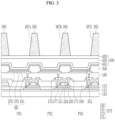
- a display device and a manufacturing method thereof according to an embodiment will now be described with reference to FIG. 12 .
- the display device and the manufacturing method thereof according to an embodiment described with reference to FIG. 12 may correspond to the display device and the manufacturing method thereof according to embodiments described with reference to FIG. 1 to FIG. 11 , so redundant description may be omitted.
- a first capping layer and a second capping layer may be further formed in an embodiment, which may be different from the previous embodiment and will now be described.
- FIG. 12 schematically shows a cross-sectional view of a display device according to an embodiment.
- the display device may include, in a like way according to a previous embodiment, a substrate 110, a transistor TFT positioned on the substrate 110, and a light-emitting device ED connected to the transistor TFT.
- An encapsulation layer 400 may be positioned on the light-emitting device ED, and a partition wall 265 including a first opening 267a, a second opening 267b, and a third opening 267c may be positioned on the encapsulation layer 400.
- the first color converting layer 520a, the low-refractive index layer 240, and the first color filter 230a may be positioned in the first opening 267a.
- the second color converting layer 520b, the low-refractive index layer 240, and the second color filter 230b may be positioned in the second opening 267b.
- the transmission layer 520c, the low-refractive index layer 240, and the third color filter 230c may be positioned in the third opening 267c.
- the low-refractive index layer 240 may be positioned on the first color converting layer 520a, the second color converting layer 520b, and the transmission layer 520c, and in an embodiment, the first capping layer 251 may be positioned on the first color converting layer 520a, the second color converting layer 520b, and the transmission layer 520c, and the low-refractive index layer 240 may be positioned on the first capping layer 251.
- the first capping layer 251 may be positioned in the first opening 267a, the second opening 267b, and the third opening 267c, and may not be positioned on the upper side of the partition wall 265.
- the first color converting layer 520a, the second color converting layer 520b, and the transmission layer 520c may be formed, then, the inorganic insulating material such as a silicon nitride (SiN x ), a silicon oxide (SiO x ), or a silicon oxynitride (SiO x N y ) may be deposited, and may be patterned to thus form the first capping layer 251.
- the first capping layer 251 may have a single-layered or multi-layered structure of the material.
- a first capping layer 251 may be positioned between the first color converting layer 520a and the low-refractive index layer 240 in the first opening 267a.
- the first capping layer 251 may be positioned on the lateral side of the partition wall 265.
- the low-refractive index layer 240 may not contact the partition wall 265 in the first opening 267a.
- the first capping layer 251 may be positioned between the low-refractive index layer 240 and the partition wall 265.
- the first capping layer 251 may be positioned between the second color converting layer 520b and the low-refractive index layer 240 in the second opening 267b.
- the first capping layer 251 may be positioned on the lateral side of the partition wall 265.
- the low-refractive index layer 240 may not contact the partition wall 265 in the second opening 267b.
- the first capping layer 251 may be positioned between the low-refractive index layer 240 and the partition wall 265.
- the first capping layer 251 may be positioned between the transmission layer 520c and the low-refractive index layer 240 in the third opening 267c.
- the first capping layer 251 may be positioned on the lateral side of the partition wall 265.
- the low-refractive index layer 240 may not contact the partition wall 265 in the third opening 267c.
- the first capping layer 251 may be positioned between the low-refractive index layer 240 and the partition wall 265.
- the first color filter 230a, the second color filter 230b, and the third color filter 230c may be positioned on the low-refractive index layer 240, and in an embodiment, the second capping layer 253 may be positioned on the low-refractive index layer 240, and the first color filter 230a, the second color filter 230b, and the third color filter 230c may be positioned on the second capping layer 253.
- the second capping layer 253 may be positioned in the first opening 267a, the second opening 267b, and the third opening 267c, and may not be positioned on the upper side of the partition wall 265.
- the inorganic insulating material such as a silicon nitride (SiN x ), a silicon oxide (SiO x ), and/or a silicon oxynitride (SiO x N y ) may be deposited, and may be patterned to thus form the second capping layer 253.
- the second capping layer 253 may have a single-layered or multi-layered structure of the material.
- the second capping layer 253 may be positioned between the low-refractive index layer 240 and the first color filter 230a in the first opening 267a.
- the second capping layer 253 may contact the bottom surface and the lateral side of the first color filter 230a.
- the second capping layer 253 may be positioned between the low-refractive index layer 240 and the second color filter 230b in the second opening 267b.
- the second capping layer 253 may contact the bottom surface and the lateral side of the second color filter 230b.
- the second capping layer 253 may be positioned between the low-refractive index layer 240 and the third color filter 230c in the third opening 267c.
- the second capping layer 253 may contact the bottom surface and the lateral side of the third color filter 230c.
- the first capping layer 251 may be positioned on a lower portion of the low-refractive index layer 240, and the second capping layer 253 may be positioned on an upper portion of the low-refractive index layer 240.
- the low-refractive index layer 240 may be protected by the first capping layer 251 and the second capping layer 253.
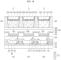
- a display device according to an embodiment will now be described with reference to FIG. 13 .
- the display device and the manufacturing method thereof according to an embodiment described with reference to FIG. 13 may correspond to the display device and the manufacturing method thereof according to an embodiment described with reference to FIG. 12 , so redundant description may be omitted.
- the first capping layer and the second capping layer may be generally formed in an embodiment, which may be different from the previous embodiment and will now be described.
- FIG. 13 schematically shows a cross-sectional view of a display device according to an embodiment.
- the display device may include, in a like way according to the previous embodiment, a substrate 110, a transistor TFT positioned on the substrate 110, and a light-emitting device ED connected to the transistor TFT.
- An encapsulation layer 400 may be positioned on the light-emitting device ED, and a partition wall 265 including a first opening 267a, a second opening 267b, and a third opening 267c may be positioned on the encapsulation layer 400.
- the first color converting layer 520a, the first capping layer 251, the low-refractive index layer 240, the second capping layer 253, and the first color filter 230a may be positioned in the first opening 267a.
- the second color converting layer 520b, the first capping layer 251, the low-refractive index layer 240, the second capping layer 253, and the second color filter 230b may be positioned in the second opening 267b.
- the transmission layer 520c, the first capping layer 251, the low-refractive index layer 240, the second capping layer 253, and the third color filter 230c may be positioned in the third opening 267c.
- a layer for forming the first capping layer 251 may be patterned so that the first capping layer 251 may not be positioned on the upper side of the partition wall 265, and in an embodiment, the first capping layer 251 may be generally formed. For example, the process for patterning the layer for forming the first capping layer 251 may not be additionally performed. The first capping layer 251 may also be positioned on the upper side of the partition wall 265.
- a layer for forming the second capping layer 253 may be patterned so that the second capping layer 253 may not be positioned on the upper side of the partition wall 265, and in an embodiment, the second capping layer 253 may be generally formed.
- the process for patterning the layer for forming the second capping layer 253 may not be additionally performed.
- the second capping layer 253 may also be positioned on the upper side of the partition wall 265.
- the first capping layer 251 and the second capping layer 253 may be positioned on the upper side of the partition wall 265.
- the low-refractive index layer 240 may be positioned between the first capping layer 251 and the second capping layer 253 in the first opening 267a, the second opening 267b, and the third opening 267c.
- the second capping layer 253 may be positioned on the first capping layer 251 on the upper side of the partition wall 265.
- the first capping layer 251 and the second capping layer 253 may be made of a same material or different materials.
- the thicknesses of the first capping layer 251 and the second capping layer 253 may be each about 4000 ⁇ , and an influence to the flatness of the upper side of the overcoat layer 290 may not be large.
- the upper side of the overcoat layer 290 may be made flat.
- the process for patterning the layers for forming the first capping layer 251 and the second capping layer 253 respectively may not be additionally performed so the processing time and cost may be reduced.
Landscapes
- Physics & Mathematics (AREA)
- Optics & Photonics (AREA)
- Engineering & Computer Science (AREA)
- Manufacturing & Machinery (AREA)
- Microelectronics & Electronic Packaging (AREA)
- Chemical & Material Sciences (AREA)
- Crystallography & Structural Chemistry (AREA)
- Inorganic Chemistry (AREA)
- Nanotechnology (AREA)
- Electroluminescent Light Sources (AREA)
- Devices For Indicating Variable Information By Combining Individual Elements (AREA)
- Optical Filters (AREA)
Abstract
Description
- The disclosure relates to a display device and a manufacturing method thereof.
- A display device is a device for displaying an image. Examples may include a liquid crystal display (LCD), an organic light emitting diode (OLED) display, and the like. A display device may be used in various electronic devices such as a mobile phone, a navigation device, a digital camera, an electronic book, a portable game machine, and various terminals.
- An organic light emitting device may include two electrodes and an organic emission layer positioned between the two electrodes, and electrons injected from one electrode and holes injected from another electrode may be combined on the organic emission layer to generate excitons. In case that the excitons change to a ground state from an excited state, the excitons output energy and emit light.
- Recently, display devices have been proposed that further include a color converting panel for the purpose of reducing optical loss and realizing a display device with high color reproducibility. The color converting panel may include semiconductor nanocrystals such as quantum dots, and may convert incident light into different colors. The color converting panel may further include scatterers.
- The organic light emitting device may be formed by combining the display panel on which light-emitting devices may be formed and the color converting panel. As parts may be respectively formed on two substrates, and they may be bonded to each other to realize the display device, the display device may become thick, an optical loss may be generated, and a manufacturing cost may increase.
- The above information disclosed in this Background section is only for enhancement of understanding of the background of the described technology, and therefore this section may contain information that does not form the prior art that is already known in this country to a person of ordinary skill in the art.
- The described technology has been made in an effort to provide a display device for reducing a thickness, an optical loss, and a manufacturing cost of a display device, and a manufacturing method thereof.
- The described technology has been made in another effort to provide a display device for planarizing an upper side of a display device and preventing generation of diffused reflection on a surface, and a manufacturing method thereof.
- An embodiment provides a display device that may include a substrate, a transistor disposed on the substrate, a light-emitting device electrically connected to the transistor, an encapsulation layer disposed on the light-emitting device, a partition wall disposed on the encapsulation layer and including an opening overlapping the light-emitting device, and a color converting layer, a low-refractive index layer, and a color filter sequentially stacked on each other in the opening.
- The partition wall may include a first opening overlapping a light-emitting device of a first pixel, a second opening overlapping a light-emitting device of a second pixel, and a third opening overlapping a light-emitting device of a third pixel.
- A first color converting layer, the low-refractive index layer, and a first color filter may be disposed in the first opening, a second color converting layer, the low-refractive index layer, and a second color filter may be disposed in the second opening, and a transmission layer, the low-refractive index layer, and a third color filter may be disposed in the third opening.
- The low-refractive index layer may be disposed on the first color converting layer, the second color converting layer, and the transmission layer, and the low-refractive index layer may be disposed on a lateral side of the partition wall.
- The low-refractive index layer may not be disposed on an upper side (which may refer to an upper surface herein) of the partition wall.
- The first color filter, the second color filter, and the third color filter may not overlap each other.
- The first color filter, the second color filter, and the third color filter may not be disposed on an upper side of the partition wall.
- The display device may further include a first capping layer and a second capping layer that are disposed in the first opening, the second opening, and the third opening. The first capping layer may be disposed between the first color converting layer and the low-refractive index layer, between the second color converting layer and the low-refractive index layer, and between the transmission layer and the low-refractive index layer, and the second capping layer may be disposed between the low-refractive index layer and the first color filter, between the low-refractive index layer and the second color filter, and between the low-refractive index layer and the third color filter.
- The first capping layer and the second capping layer may be disposed on an upper side of the partition wall.
- The display device may further include an overcoat layer disposed on the first color filter, the second color filter, the third color filter, and the partition wall.
- Another embodiment provides a method for manufacturing a display device. The method may include forming a transistor and a light-emitting device electrically connected to the transistor on a substrate, forming an encapsulation layer on the light-emitting device, forming a layer for forming a partition wall on the encapsulation layer, forming an opening overlapping the light-emitting device by patterning the layer for forming the partition wall, forming a color converting layer in the opening, forming a low-refractive index layer in the opening, and forming a color filter in the opening.
- The forming of the color converting layer, the forming of the low-refractive index layer, and the forming of the color filter may be performed by using an inkjet printing process.
- The patterning of the layer for forming the partition wall may include forming a first opening overlapping a light-emitting device of a first pixel, a second opening overlapping a light-emitting device of a second pixel, and a third opening overlapping a light-emitting device of a third pixel.
- The forming of the color converting layer may include by dropping different ink materials into the first opening, the second opening, and the third opening, forming a first color converting layer in the first opening, forming a second color converting layer in the second opening, and forming a transmission layer in the third opening.
- The forming of the low-refractive index layer may include by dropping a same ink material into the first opening, the second opening, and the third opening, forming a low-refractive index layer on the first color converting layer, the second color converting layer, and the transmission layer.
- The low-refractive index layer may be disposed on a lateral side of the partition wall, and the low-refractive index layer may not be disposed on an upper side of the partition wall.
- The forming of the color filter may include by dropping different ink materials in the first opening, the second opening, and the third opening, forming a first color filter in the first opening, forming a second color filter in the second opening, and forming a third color filter in the third opening. The first color filter, the second color filter, and the third color filter may be disposed on the low-refractive index layer.
- The first color filter, the second color filter, and the third color filter may not overlap each other, and the first color filter, the second color filter, and the third color filter may not be disposed on an upper side of the partition wall.
- The method may further include, before the forming of the low-refractive index layer, forming a first capping layer on the first color converting layer, the second color converting layer, and the transmission layer, and after the forming of the low-refractive index layer, forming a second capping layer on the low-refractive index layer.
- The method may further include forming an overcoat layer on the first color filter, the second color filter, the third color filter, and the partition wall.
- According to the embodiments, parts such as the light-emitting devices and the color converting layers may be formed on one substrate, thereby reducing the thickness of the display device, the optical loss, and the manufacturing cost.
- Further, the upper side of the display device may be planarized, thereby preventing generation of the diffused reflection on the surface.
-
-
FIG. 1 schematically shows a cross-sectional view of a display device according to an embodiment. -
FIG. 2 to FIG. 5 ,FIG. 10 , andFIG. 11 schematically show cross-sectional views in order of a process for manufacturing a display device according to an embodiment. -
FIG. 6 andFIG. 8 schematically show a flat surface of a layer in a process for manufacturing a display device according to an embodiment. -
FIG. 7 andFIG. 9 schematically show cross-sectional views of a layer in a process for manufacturing a display device according to an embodiment. -
FIG. 12 schematically shows a cross-sectional view of a display device according to an embodiment. -
FIG. 13 schematically shows a cross-sectional view of a display device according to an embodiment. - The disclosure will be described more fully hereinafter with reference to the accompanying drawings, in which embodiments of the disclosure are shown. As those skilled in the art would realize, the described embodiments may be modified in various different ways, all without departing from the spirit or scope of the disclosure.
- As used herein, the singular forms, "a," "an," and "the" are intended to include the plural forms as well, unless the context clearly indicates otherwise.
- In the specification and the claims, the phrase "at least one of" is intended to include the meaning of "at least one selected from the group of" for the purpose of its meaning and interpretation. For example, "at least one of A and B" may be understood to mean "A, B, or A and B." In the specification and the claims, the term "and/or" is intended to include any combination of the terms "and" and "or" for the purpose of its meaning and interpretation. For example, "A and/or B" may be understood to mean "A, B, or A and B." The terms "and" and "or" may be used in the conjunctive or disjunctive sense and may be understood to be equivalent to "and/or."
- Parts that may be less helpful to the description will be omitted to more clearly describe the disclosure, and the same elements will be designated by the same reference numerals throughout the specification.
- The size and thickness of each configuration shown in the drawings may be arbitrarily shown for better understanding and ease of description, but the disclosure is not limited thereto.
- It will be understood that when an element such as a layer, film, region, or substrate is referred to as being "on" another element, the element can be directly on the other element or intervening elements may also be present. In contrast, when an element is referred to as being "directly on" another element, there may be no intervening elements present. Terms such as "on", "above", "upper", "lower", "side", and the like, are spatially relative concepts, and are used only for ease of description. For example, the word "on" or "above" means positioned on or below the object portion, and does not necessarily mean positioned on the upper side of the object portion based on a gravitational direction.
- It will be understood that the terms "connected to" or "coupled to" may include a physical or electrical connection or coupling.
- The terms "overlap" or "overlapped" mean that a first object may be above or below or to a side of a second object, and vice versa. Additionally, the term "overlap" may include layer, stack, face or facing, extending over, covering, or partly covering or any other suitable term as would be appreciated and understood by those of ordinary skill in the art.
- When an element is described as "not overlapping" or to "not overlap" another element, this may include that the elements are spaced apart from each other, offset from each other, or set aside from each other or any other suitable term as would be appreciated and understood by those of ordinary skill in the art.
- Unless explicitly described to the contrary, terms such as "comprise", "has", "having", and "includes", and variations thereof, will be understood to imply the inclusion of stated elements but not the exclusion of any other elements.
- The phrase "in a plan view" means viewing an object portion from a position, e.g., viewing from a top position. The phrase "in a cross-sectional view" means viewing a cross-section of which the object portion is cut from a position, e.g., viewing a vertically cut view from a side.
- "About" or "approximately" or "substantially" as used herein is inclusive of the stated value and means within an acceptable range of deviation for the particular value as determined by one of ordinary skill in the art, considering the measurement in question and the error associated with measurement of the particular quantity (i.e., the limitations of the measurement system). For example, "about" may mean within one or more standard deviations, or within ± 30%, 20%, 10%, 5% of the stated value.
- Unless otherwise defined, all terms (including technical and scientific terms) used herein have the same meaning as commonly understood by one of ordinary skill in the art to which the disclosure pertains. It will be further understood that terms, such as those defined in commonly used dictionaries, should be interpreted as having a meaning that is consistent with their meaning in the context of the relevant art and will not be interpreted in an idealized or overly formal sense unless expressly so defined herein.
- A display device according to an embodiment will now be described with reference to
FIG. 1 . -
FIG. 1 schematically shows a cross-sectional view of a display device according to an embodiment. - As shown in
FIG. 1 , the display device according to an embodiment may include asubstrate 110, a transistor TFT positioned (disposed) on thesubstrate 110, and a light-emitting device ED connected to the transistor TFT. - The
substrate 110 may include at least one of polystyrene, polyvinyl alcohol, polymethyl methacrylate, polyethersulfone, polyacrylate, polyetherimide, polyethylene naphthalate, polyethylene terephthalate, polyphenylene sulfide, polyarylate, polyimide, polycarbonate, triacetate cellulose, and cellulose acetate propionate. Thesubstrate 110 may be a rigid substrate or a flexible substrate that may be bent, folded, or rolled. Thesubstrate 110 may be a single layer or a multilayer. Thesubstrate 110 may be made by alternately stacking at least one base layer including sequentially stacked polymer resins and at least one organic layer. - A surface of the
substrate 110 may be made flat. Abuffer layer 111 may include an inorganic insulating material such as a silicon nitride (SiNx), a silicon oxide (SiOx), and/or a silicon oxynitride (SiOxNy), and/or an organic insulating material. Thebuffer layer 111 may have a single-layered or multi-layered structure of the material. A barrier layer (not shown) may be further positioned on thesubstrate 110. The barrier layer may be positioned between thesubstrate 110 and thebuffer layer 111. The barrier layer may include an inorganic insulating material such as a silicon nitride (SiNx), a silicon oxide (SiOx), and/or a silicon oxynitride (SiOxNy). The barrier layer may have a single-layered or multi-layered structure of the material. - A
light blocking layer 177 may be positioned on thebuffer layer 111. Thelight blocking layer 177 may block light input to asemiconductor 131. Thelight blocking layer 177 may overlap thesemiconductor 131, and may have a greater width than thesemiconductor 131. - An insulating
layer 113 may be positioned on thelight blocking layer 177. The insulatinglayer 113 may include an inorganic insulating material such as a silicon nitride (SiNx), a silicon oxide (SiOx), and/or a silicon oxynitride (SiOxNy), and/or an organic insulating material. The insulatinglayer 113 may improve a characteristic of thesemiconductor 131 by blocking an inflow of impurities to thesemiconductor 131 from thesubstrate 110. - The
semiconductor 131 may be positioned on the insulatinglayer 113. Thesemiconductor 131 may include at least one of amorphous silicon, polycrystalline silicon, and an oxide semiconductor. For example, thesemiconductor 131 may include a low temperature polysilicon (LTPS) and/or an oxide semiconductor material including at least one of zinc (Zn), indium (In), gallium (Ga), tin (Sn), or a combination thereof. For example, thesemiconductor 131 may include an indium-gallium-zinc oxide (IGZO). Thesemiconductor 131 may include a channel region, a source region, and a drain region distinguished by whether impurities may be doped. The source region and the drain region may have a conductive characteristic that corresponds to a conductor. - A
gate insulating layer 120 may be positioned on thesemiconductor 131. Thegate insulating layer 120 may have a single-layered or multi-layered structure. Thegate insulating layer 120 may include an inorganic insulating material such as a silicon nitride (SiNx), a silicon oxide (SiOx), and/or a silicon oxynitride (SiOxNy). Thegate insulating layer 120 may cover at least part of thesemiconductor 131. For example, thegate insulating layer 120 may overlap the channel region of thesemiconductor 131. Thegate insulating layer 120 may not overlap the source region and the drain region of thesemiconductor 131. However, without being limited thereto, thegate insulating layer 120 may generally cover thesemiconductor 131. Thegate insulating layer 120 may be generally positioned on thesubstrate 110. - A
gate electrode 124 may be positioned on thegate insulating layer 120. Thegate electrode 124 may include a metal such as copper (Cu), molybdenum (Mo), aluminum (Al), silver (Ag), chromium (Cr), tantalum (Ta), or titanium (Ti), or a metal alloy thereof. Thegate electrode 124 may be configured with a single layer or a multilayer. A region of thesemiconductor 131 overlapping thegate electrode 124 in a plan view may be a channel region. In case that thegate electrode 124 is formed, a doping process or a plasma process may be performed. A portion of thesemiconductor 131 covered by thegate electrode 124 may not be doped or plasma processed, and a portion of thesemiconductor 131 not covered by thegate electrode 124 may be doped or plasma processed to thus have a same characteristic as the conductor. For example, the source region and the drain region of thesemiconductor 131 may not overlap thegate electrode 124, and may be doped or plasma processed to have the same characteristic as the conductor. - A first
interlayer insulating layer 160 may be positioned on thegate electrode 124. The firstinterlayer insulating layer 160 may be generally formed on thesubstrate 110. For example, the firstinterlayer insulating layer 160 may cover thegate insulating layer 120, thesemiconductor 131, and the insulatinglayer 113. The firstinterlayer insulating layer 160 may have a single-layered or multi-layered structure. The firstinterlayer insulating layer 160 may include an inorganic insulating material and/or an organic insulating material. - A
source electrode 173 and adrain electrode 175 may be positioned on the firstinterlayer insulating layer 160. Thesource electrode 173 and thedrain electrode 175 may include a metal such as aluminum (Al), copper (Cu), silver (Ag), gold (Au), platinum (Pt), palladium (Pd), nickel (Ni), molybdenum (Mo), tungsten (W), titanium (Ti), chromium (Cr), or tantalum (Ta), or a metal alloy thereof. Thesource electrode 173 anddrain electrode 175 may be configured with a single layer or a multilayer. Thesource electrode 173 and thedrain electrode 175 may be configured to be a triple layer including an upper layer, an intermediate layer, and a lower layer, and the upper layer and the lower layer may include titanium (Ti), and the intermediate layer may include aluminum (Al). - The first
interlayer insulating layer 160 may include asource electrode 173 and an opening overlapping the source region of thesemiconductor 131. Thesource electrode 173 may be connected to the source region of thesemiconductor 131 through the opening formed in the firstinterlayer insulating layer 160. The firstinterlayer insulating layer 160 may include adrain electrode 175 and an opening overlapping the drain region of thesemiconductor 131. Thedrain electrode 175 may be connected to the drain region of thesemiconductor 131 through the opening formed in the firstinterlayer insulating layer 160. The firstinterlayer insulating layer 160 may further include an opening overlapping thedrain electrode 175 and thelight blocking layer 177. The opening may be made in the insulatinglayer 113. Thedrain electrode 175 may be connected to thelight blocking layer 177 through the opening made in the firstinterlayer insulating layer 160 and the insulatinglayer 113. - The above-noted
semiconductor 131, thegate electrode 124, thesource electrode 173, and thedrain electrode 175 may configure one transistor TFT. Depending on embodiments, the transistor TFT may include the source region and the drain region of thesemiconductor 131 instead of thesource electrode 173 and thedrain electrode 175. - The display device according to an embodiment may include a first pixel PX1, a second pixel PX2, and a third pixel PX3. One first pixel PX1, one second pixel PX2, and one third pixel PX3 are shown, and without being limited thereto, the display device according to an embodiment may include multiple first pixels PX1, multiple second pixels PX2, and multiple third pixels PX3. The first pixels PX1, the second pixels PX2, and the third pixels PX3 may be disposed in various ways. One transistor TFT is shown to be disposed in each of the first pixel PX1, the second pixel PX2, and the third pixel PX3, and without being limited thereto, multiple transistors TFT may be positioned in each of the first pixels PX1, the second pixels PX2, and the third pixels PX3. For example, a switching transistor and a driving transistor may be positioned in each of the first pixel PX1, the second pixels PX2, and the third pixels PX3. Although not shown, at least one capacitor may be positioned in each of the first pixels PX1, the second pixels PX2, and the third pixels PX3.
- A second
interlayer insulating layer 180 may be positioned on thesource electrode 173 and thedrain electrode 175. The secondinterlayer insulating layer 180 may cover thesource electrode 173, thedrain electrode 175, and the firstinterlayer insulating layer 160. The secondinterlayer insulating layer 180 may planarize the surface of thesubstrate 110 on which transistors TFT may be installed, may be an organic insulator, and may include at least one material of a polyimide, a polyamide, an acryl resin, benzocyclobutene, and a phenol resin. - A
pixel electrode 191 may be positioned on the secondinterlayer insulating layer 180. Thepixel electrode 191 may also be referred to as an anode, and may be a single layer including a transparent conductive oxide film or a metal material, or a multilayer including the same. The transparent conductive oxide film may include an indium tin oxide (ITO), a poly-ITO, an indium zinc oxide (IZO), an indium gallium zinc oxide (IGZO), and/or an indium tin zinc oxide (ITZO). The metal material may include silver (Ag), molybdenum (Mo), copper (Cu), gold (Au), and/or aluminum (Al). - The second
interlayer insulating layer 180 may include an opening overlapping thepixel electrode 191 and thedrain electrode 175. Thepixel electrode 191 may be connected to thedrain electrode 175 through the opening of the secondinterlayer insulating layer 180. Accordingly, thepixel electrode 191 may receive an output current to be transmitted to theemission layer 370 from thedrain electrode 175. - A
bank layer 350 may be positioned on thepixel electrode 191 and the secondinterlayer insulating layer 180. Thebank layer 350 may also be referred to as a pixel defining layer (PDL), and includes apixel opening 351 overlapping at least part of thepixel electrode 191. Thepixel opening 351 may overlap a center portion of thepixel electrode 191, and may not overlap an edge of thepixel electrode 191. Therefore, thepixel opening 351 may be smaller than thepixel electrode 191. Thebank layer 350 may partition a formation position of theemission layer 370 so that theemission layer 370 may be positioned on a portion in which an upper side of thepixel electrode 191 may be exposed. Thebank layer 350 may be an organic insulator including at least one material of a polyimide, a polyamide, an acryl resin, benzocyclobutene, and a phenol resin. Depending on embodiments, thebank layer 350 may be formed with a black pixel defining layer (BPDL) including a black color pigment. - The
bank layer 350 may be positioned on a boundary between the first pixel PX1 and the second pixel PX2, between the second pixel PX2 and the third pixel PX3, and between the third pixel PX3 and the first pixel PX1. For example, thebank layer 350 may be positioned on the boundary among pixels. -
Multiple pixel openings 351 may each have a similar shape to thepixel electrode 191 in a plan view. For example, thepixel opening 351 and thepixel electrode 191 may substantially have polygonal shapes in a plan view. Corners of thepixel opening 351 and thepixel electrode 191 may be chamfered. The shapes of thepixel opening 351 and thepixel electrode 191 are not limited thereto, and may be modifiable in many ways. - In this instance,
multiple pixel electrodes 191 corresponding to the respective first pixel PX1, the second pixel PX2, and the third pixel PX3 may have different sizes in a plan view. In a like manner,multiple pixel openings 351 corresponding to the respective first pixel PX1, the second pixel PX2, and the third pixel PX3 may have different sizes in a plan view. For example, thepixel opening 351 and thepixel electrode 191 corresponding to the first pixel PX1 may have greater sizes than thepixel opening 351 and thepixel electrode 191 corresponding to the second pixel PX2 in a plan view. Thepixel opening 351 and thepixel electrode 191 corresponding to the first pixel PX1 may have smaller or similar sizes than/to thepixel opening 351 and thepixel electrode 191 corresponding to the third pixel PX3 in a plan view. However, without being limited thereto, therespective pixel opening 351 and thepixel electrode 191 may be set to have various sizes. - An
emission layer 370 may be positioned in thepixel opening 351 partitioned by thebank layer 350. However, without being limited thereto, theemission layer 370 may be positioned on thebank layer 350 as well as in thepixel opening 351. For example, theemission layer 370 may be generally formed on thesubstrate 110. Theemission layer 370 may be formed by performing a deposition process by using an open mask of which a portion corresponding to the display area may be opened. Theemission layer 370 may include a low molecular or polymer organic material. Theemission layer 370 is shown to be a single layer, and in actuality, auxiliary layers such as an electron injecting layer, an electron transport layer, a hole transport layer, and a hole injecting layer may be included above/below theemission layer 370. The hole injecting layer and the hole transport layer may be positioned on a lower portion of theemission layer 370, and the electron transport layer and the electron injecting layer may be positioned on an upper portion of theemission layer 370. Another emission layer may be further positioned on theemission layer 370. For example, at least twoemission layers 370 may be stacked on each other. - Although not shown, a spacer may be further positioned on the
bank layer 350. The spacer may include a same material as thebank layer 350. However, without being limited thereto, the spacer may be made of a material that may be different from that of thebank layer 350. The spacer may be an organic insulator including at least one material of a polyimide, a polyamide, an acryl resin, benzocyclobutene, and a phenol resin. - The
common electrode 270 may be positioned on thebank layer 350 and theemission layer 370. Thecommon electrodes 270 of the respective first pixel PX1, the second pixel PX2, and the third pixel PX3 may be connected to each other. Thecommon electrodes 270 may be formed to be generally connected to each other on thesubstrate 110. Thecommon electrodes 270 may also be referred to as a cathode, and may be made of a transparent conductive layer including an indium tin oxide (ITO), an indium zinc oxide (IZO), an indium gallium zinc oxide (IGZO), and/or an indium tin zinc oxide (ITZO). Thecommon electrodes 270 may be made of a metal material such as silver (Ag), magnesium (Mg), or a mixture thereof. Thicknesses of thecommon electrodes 270 may be adjusted to be formed as a transparent conductive layer. Thecommon electrodes 270 may have a semi-transparent characteristic, and may configure a microcavity with thepixel electrode 191. - The
pixel electrode 191, theemission layer 370, and thecommon electrode 270 may configure a light-emitting device ED. In the first pixel PX1, the second pixel PX2, and the third pixel PX3, portions overlapping thepixel electrode 191, theemission layer 370, and thecommon electrode 270 may become light emitting regions of the respective light-emitting devices ED. - An
encapsulation layer 400 may be positioned on thecommon electrode 270. Theencapsulation layer 400 may include at least one inorganic film and/or at least one organic film. In an embodiment, theencapsulation layer 400 may include a firstinorganic encapsulation layer 410, anorganic encapsulation layer 420, and a secondinorganic encapsulation layer 430. However, the number of inorganic films and organic films configuring theencapsulation layer 400 may be modifiable in many ways. The display device according to an embodiment may include a display area for displaying a screen and a peripheral area for surrounding the display area. The firstinorganic encapsulation layer 410, theorganic encapsulation layer 420, and the secondinorganic encapsulation layer 430 may be positioned in part of the display area and the peripheral area. Depending on embodiments, theorganic encapsulation layer 420 may be formed around the display area, and the firstinorganic encapsulation layer 410 and the secondinorganic encapsulation layer 430 may be formed up to the peripheral area. Theencapsulation layer 400 may protect the light-emitting device ED from moisture or oxygen that may be input from the outside, and end portions of the firstinorganic encapsulation layer 410 and the secondinorganic encapsulation layer 430 may be formed to directly contact each other. - A
partition wall 265 may be positioned on theencapsulation layer 400. Thepartition wall 265 may overlap thebank layer 350. Thepartition wall 265 may be positioned on the boundary among the respective first pixel PX1, the second pixel PX2, and the third pixel PX3. Thepartition wall 265 may be made of a photosensitive resin. Thepartition wall 265 may include a colored pigment such as a black pigment or a blue pigment. A thickness of thepartition wall 265 may be equal to or greater than about 10 µm and equal to or less than about 20 µm. A width of thepartition wall 265 may be gradually reduced going away from theencapsulation layer 400. The width of thepartition wall 265 may be gradually reduced going away from thesubstrate 110. However, without being limited thereto, the width of thepartition wall 265 may be constant. In yet another embodiment, the width of thepartition wall 265 may be gradually increased going away from thesubstrate 110. - The
partition wall 265 may includeopenings openings first opening 267a, asecond opening 267b, and athird opening 267c. Thefirst opening 267a may overlap the light emitting region of the light-emitting device ED of the first pixel PX1, thesecond opening 267b may overlap the light emitting region of the light-emitting device ED of the second pixel PX2, and thethird opening 267c may overlap the light emitting region of the light-emitting device ED of the third pixel PX3. Theopenings partition wall 265 may overlap thepixel opening 351 of thebank layer 350. Thefirst opening 267a, thesecond opening 267b, and thethird opening 267c may be separated from each other by thepartition wall 265. For example, thefirst opening 267a, thesecond opening 267b, and thethird opening 267c may be surrounded by thepartition wall 265. - A first
color converting layer 520a may be positioned in thefirst opening 267a, a secondcolor converting layer 520b may be positioned in thesecond opening 267b, and atransmission layer 520c may be positioned in thethird opening 267c. - The first
color converting layer 520a may convert light input from the light-emitting device ED of the first pixel PX1 into light with a first wavelength. Light with a first wavelength may be red light with a maximum light-emitting peak wavelength of about 600 nm to about 650 nm, for example, about 620 nm to about 650 nm. The firstcolor converting layer 520a may includefirst quantum dots 521a andscatterers 530. - The second
color converting layer 520b may convert light input from the light-emitting device ED of the second pixel PX2 into light with a second wavelength. Light with a second wavelength may be green light with the maximum light-emitting peak wavelength of about 500 nm to about 550 nm, for example, about 510 nm to about 550 nm. The secondcolor converting layer 520b may include secondquantum dots 521b andscatterers 530. - The
transmission layer 520c may transmit light input from the light-emitting device ED of the third pixel PX3. The light having been transmitted through thetransmission layer 520c may be light with a third wavelength. Light with a third wavelength may be blue light with the maximum light-emitting peak wavelength of about 380 nm to about 480 nm, for example, equal to or greater than about 420 nm, equal to or greater than about 430 nm, equal to or greater than about 440 nm, or equal to or greater than about 445 nm and equal to or less than about 470 nm, equal to or less than about 460 nm, or equal to or less than about 455 nm. Thetransmission layer 520c may includescatterers 530. - The
scatterers 530 may increase light efficiency by scattering the light input to the firstcolor converting layer 520a, the secondcolor converting layer 520b, and thetransmission layer 520c. - The
first quantum dot 521a and the secondquantum dot 521b (also referred to as semiconductor nanocrystals) may independently include a group II-VI compound, a group III-V compound, a group IV-VI compound, a group IV element or compound, a group I-III-VI compound, a group II-III-VI compound, a group I-II-IV-VI compound, or a combination thereof. The quantum dots (e.g., at least one of thefirst quantum dot 521a and the secondquantum dot 521b, similar to this hereinafter) may not include cadmium. - The group II-VI compound may be selected from a binary element compound selected from among CdSe, CdTe, ZnS, ZnSe, ZnTe, ZnO, HgS, HgSe, HgTe, MgSe, MgS, or a combination thereof; a ternary element compound selected from among CdSeS, CdSeTe, CdSTe, ZnSeS, ZnSeTe, ZnSTe, HgSeS, HgSeTe, HgSTe, CdZnS, CdZnSe, CdZnTe, CdHgS, CdHgSe, CdHgTe, HgZnS, HgZnSe, HgZnTe, MgZnSe, MgZnS, or a combination thereof; and a quaternary element compound selected from among CdZnSeS, CdZnSeTe, CdZnSTe, CdHgSeS, CdHgSeTe, CdHgSTe, HgZnSeS, HgZnSeTe, HgZnSTe, or a combination thereof. The group II-VI compound may further include a group III metal.
- The group III-V compound may be selected from a binary element compound selected from among GaN, GaP, GaAs, GaSb, AIN, AIP, AlAs, AlSb, InN, InP, InAs, InSb, or a combination thereof; a ternary element compound selected from among GaNP, GaNAs, GaNSb, GaPAs, GaPSb, AINP, AINAs, AINSb, AIPAs, AlPSb, InNP, InNAs, InNSb, InPAs, InPSb, or a combination thereof; and a quaternary element compound selected from among GaAINP, GaAINAs, GaAINSb, GaAIPAs, GaAIPSb, GalnNP, GalnNAs, GaInNSb, GalnPAs, GalnPSb, InAINP, InAINAs, InAINSb, InAIPAs, InAIPSb, or a combination thereof. The group III-V compound may further include a group II metal (e.g., InZnP).
- The group IV-VI compound may be selected from a binary element compound selected from among SnS, SnSe, SnTe, PbS, PbSe, PbTe, or a combination thereof; a ternary element compound selected from among SnSeS, SnSeTe, SnSTe, PbSeS, PbSeTe, PbSTe, SnPbS, SnPbSe, SnPbTe, or a combination thereof; and a quaternary element compound selected from among SnPbSSe, SnPbSeTe, SnPbSTe, or a combination thereof.
- The group IV element or compound may be selected from a singular element material selected from among Si, Ge, or a combination thereof; and a binary element compound selected from among SiC, SiGe, or a combination thereof, and is not limited thereto.
- Examples of the group I-III-VI compound include CuInSe2, CuInS2, CuInGaSe, and CulnGaS, but are not limited thereto.
- Examples of the group I-II-IV-VI compound include CuZnSnSe and CuZnSnS, but are not limited thereto. The group IV element or compound may be a single element selected from among Si, Ge, or a combination thereof, or a binary compound selected from among SiC, SiGe, or a combination thereof.
- The group II-III-VI compound may be selected from among ZnGaS, ZnAIS, ZnlnS, ZnGaSe, ZnAlSe, ZnlnSe, ZnGaTe, ZnAITe, ZnlnTe, ZnGaO, ZnAlO, ZnlnO, HgGaS, HgAIS, HglnS, HgGaSe, HgAISe, HglnSe, HgGaTe, HgAITe, HglnTe, MgGaS, MgAIS, MglnS, MgGaSe, MgAISe, MglnSe, and a combination thereof, but are not limited thereto.
- The group I-II-IV-VI compound may be selected from among CuZnSnSe and CuZnSnS, but are not limited thereto.
- In an embodiment, the quantum dots may not include cadmium. The quantum dots may include semiconductor nanocrystals based on the group III-V compound including indium and phosphorus. The group III-V compound may further include zinc. The quantum dots may include a semiconductor nanocrystal based on the group II-VI compound including a chalcogen (e.g., sulfur, selenium, tellurium, or a combination thereof) and zinc.
- Regarding the quantum dot, the above-described binary compound, the tertiary compound, and/or the quaternary compound may exist in the particles with uniform concentration, or may exist in the same particles with a concentration distribution partially divided into some states. Further, the color conversion media layer (which may include the first
color converting layer 520a and the secondcolor converting layer 520b, for example) may have a core-shell structure where one quantum dot surrounds another quantum dot. An interface between the core and the shell may have a concentration gradient such that a concentration of an element existing in the shell may be gradually reduced nearing the center thereof. - In some embodiments, the quantum dot may have a core-shell structure including a core including the above-described nanocrystal and a shell surrounding the core. The shell of the quantum dot may function as a protective layer for maintaining the semiconductor characteristic by preventing chemical denaturation of the core and/or a charging layer for providing an electrophoretic characteristic to the quantum dot. The shell may be a single layer or a multilayer. An interface between the core and the shell may have a concentration gradient such that a concentration of an element existing in the shell may be gradually reduced nearing the center thereof. Examples of the shell of the quantum dot include a metallic or non-metallic oxide, a semiconductor compound, or a combination thereof.
- For example, the metallic or non-metallic oxide may include binary compounds such as SiO2, Al2O3, TiO2, ZnO, MnO, Mn2O3, Mn3O4, CuO, FeO, Fe2O3, Fe3O4, CoO, Co3O4, and/or NiO, or tertiary compounds such as MgAl2O4, CoFe2O4, NiFezOa, and/or CoMn2O4, but the disclosure is not limited thereto.
- The semiconductor compound may include CdS, CdSe, CdTe, ZnS, ZnSe, ZnTe, ZnSeS, ZnTeS, GaAs, GaP, GaSb, HgS, HgSe, HgTe, InAs, InP, InGaP, InSb, AlAs, AIP, and/or AlSb, and the disclosure is not limited thereto.
- An interface between the core and the shell may have a concentration gradient such that a concentration of an element existing in the shell may be gradually reduced nearing the center thereof. The semiconductor nanocrystal may have a structure including a semiconductor nanocrystal core and a multi-layered shell surrounding the semiconductor nanocrystal core. In an embodiment, the multi-layered shell may have two or more layers, for example, two, three, four, five, or more layers. The two adjacent layers of the shell may have a single composition or different compositions. In the multi-layered shell, each layer may have a composition that varies along the radius.
- The quantum dots may have a full width at half maximum (FWHM) of a light-emitting wavelength spectrum that may be less than about 45 nm, less than about 40 nm, or less than about 30 nm, and color purity or color reproducibility may be improved within this range. Further, light emitted through the quantum dot may be output in all directions, thereby improving a light viewing angle.
- Regarding the quantum dots, a shell material and a core material may have different energy bandgaps. For example, the energy bandgap of the shell material may be greater than that of the core material. In another embodiment, the energy bandgap of the shell material may be less than that of the core material. The quantum dots may have a multi-layered shell. Regarding the multi-layered shell, the energy bandgap of an outer layer may be greater than the energy bandgap of an inner layer (i.e., a layer that may be near the core). Regarding the multi-layered shell, the energy bandgap of the outer layer may be less than the energy bandgap of the inner layer.
- The quantum dots may adjust the absorption/emission wavelength by adjusting the composition and the size thereof. The maximum light-emitting peak wavelength of the quantum dots may have a wavelength range from ultraviolet to infrared or higher.
- The quantum dots may include an organic ligand (e.g., having a hydrophobic residue and/or a hydrophilic residue). The organic ligand residue may be combined to the surface of the quantum dot. The organic ligand may include RCOOH, RNH2, R2NH, R3N, RSH, R3PO, R3P, ROH, RCOOR, RPO (OH)2, RHPOOH, R2POOH, or a combination thereof, and here, R may independently be a C3 to C40 substituted or unsubstituted aliphatic hydrocarbon group such as a C3 to C40 (e.g., C5 to C24) substituted or unsubstituted alkyl group, or a substituted or unsubstituted alkenyl group, a C6 to C40 (e.g., C6 to C20) substituted or unsubstituted aromatic hydrocarbon group such as a C6 to C40 substituted or unsubstituted aryl group, or a combination thereof.
- Examples of the organic ligand may include thiol compounds such as methane thiol, ethane thiol, propane thiol, butane thiol, pentane thiol, hexane thiol, octane thiol, dodecane thiol, hexadecane thiol, octadecane thiol, and/or benzyl thiol; amines such as methane amine, ethane amine, propane amine, butane amine, pentyl amine, hexyl amine, octyl amine, nonylamine, decylamine, dodecyl amine, hexadecyl amine, octadecyl amine, dimethyl amine, diethyl amine, dipropyl amine, tributylamine, and/or trioctylamine; carboxylic acid compounds such as methanoic acid, ethanoic acid, propanoic acid, butanoic acid, pentanoic acid, hexanoic acid, heptanoic acid, octanoic acid, dodecanoic acid, hexadecanoic acid, octadecanoic acid, oleic acid, and/or benzoic acid; phosphine compounds such as methyl phosphine, ethyl phosphine, propyl phosphine, butyl phosphine, pentyl phosphine, octyl phosphine, dioctyl phosphine, tributyl phosphine, and/or trioctyl phosphine; phosphine compounds or their oxide compounds such as methyl phosphine oxide, ethyl phosphine oxide, propyl phosphine oxide, butyl phosphine oxide, pentyl phosphine oxide, tributyl phosphine oxide, octyl phosphine oxide, dioctyl phosphine oxide, and/or trioctyl phosphine oxide; diphenyl phosphine, or a triphenyl phosphine compound or oxide compounds thereof; C5 to C20 alkyl phosphinic acids such as hexyl phosphinic acid, octyl phosphinic acid, dodecane phosphinic acid, tetradecane phosphinic acid, hexadecane phosphinic acid, and/or octadecane phosphinic acid; and C5 to C20 alkyl phosphonic acids. The quantum dot may include the organic ligand alone or as a mixture of at least one kind. The hydrophobic organic ligand may not include a photopolymerizable residue (e.g., acrylate or methacrylate).
- A low-
refractive index layer 240 may be positioned on the firstcolor converting layer 520a, the secondcolor converting layer 520b, and thetransmission layer 520c. The low-refractive index layer 240 may be positioned in thefirst opening 267a, thesecond opening 267b, and thethird opening 267c. The low-refractive index layer 240 may be positioned on the firstcolor converting layer 520a in thefirst opening 267a, and may cover a lateral side of thepartition wall 265. The low-refractive index layer 240 may be positioned on the secondcolor converting layer 520b in thesecond opening 267b, and may cover the lateral side of thepartition wall 265. The low-refractive index layer 240 may be positioned on thetransmission layer 520c in thethird opening 267c, and may cover the lateral side of thepartition wall 265. The low-refractive index layer 240 may include an organic material or an inorganic material with a low refractive index. For example, the refractive index of the low-refractive index layer 240 may be equal to or greater than about 1.1 and equal to or less than about 1.3. - A
first color filter 230a, asecond color filter 230b, and athird color filter 230c may be positioned on the low-refractive index layer 240. Thefirst color filter 230a may be positioned in thefirst opening 267a, thesecond color filter 230b may be positioned in thesecond opening 267b, and thethird color filter 230c may be positioned in thethird opening 267c. - The
first color filter 230a may transmit light with a first wavelength and may absorb light with other wavelengths so thefirst color filter 230a may increase purity of light with a first wavelength discharged to an outside of the display device. Thefirst color filter 230a may be surrounded by the low-refractive index layer 240 in thefirst opening 267a. A bottom surface and a lateral side of thefirst color filter 230a may contact the low-refractive index layer 240. Thefirst color filter 230a may not contact thepartition wall 265. Thefirst color filter 230a may overlap the firstcolor converting layer 520a. The low-refractive index layer 240 may be positioned between thefirst color filter 230a and the firstcolor converting layer 520a. - The
second color filter 230b may transmit light with a second wavelength and may absorb light with other wavelengths so thesecond color filter 230b may increase purity of light with a second wavelength discharged to the outside of the display device. Thesecond color filter 230b may be surrounded by the low-refractive index layer 240 in thesecond opening 267b. A bottom surface and a lateral side of thesecond color filter 230b may contact the low-refractive index layer 240. Thesecond color filter 230b may not contact thepartition wall 265. Thesecond color filter 230b may overlap the secondcolor converting layer 520b. The low-refractive index layer 240 may be positioned between thesecond color filter 230b and the secondcolor converting layer 520b. - The
third color filter 230c may transmit light with a third wavelength and may absorb light with other wavelengths so thethird color filter 230c may increase purity of light with a third wavelength discharged to the outside of the display device. Thethird color filter 230c may be surrounded by the low-refractive index layer 240 in thethird opening 267c. A bottom surface and a lateral side of thethird color filter 230c may contact the low-refractive index layer 240. Thethird color filter 230c may not contact thepartition wall 265. Thethird color filter 230c may overlap thetransmission layer 520c. The low-refractive index layer 240 may be positioned between thethird color filter 230c and thetransmission layer 520c. - The
first color filter 230a, thesecond color filter 230b, and thethird color filter 230c have been described to not contact thepartition wall 265, but are not limited thereto. Depending on cases, at least some of thefirst color filter 230a, thesecond color filter 230b, and thethird color filter 230c may contact thepartition wall 265. - A thickness of the
partition wall 265 may correspond to thicknesses of the firstcolor converting layer 520a, the low-refractive index layer 240, and thefirst color filter 230a. For example, the thickness of thepartition wall 265 may be equal to or greater than a sum of the thicknesses of the firstcolor converting layer 520a, the low-refractive index layer 240, and thefirst color filter 230a. The thickness of thepartition wall 265 may correspond to the thicknesses of the secondcolor converting layer 520b, the low-refractive index layer 240, and thesecond color filter 230b. For example, the thickness of thepartition wall 265 may be equal to or greater than a sum of the thicknesses of the secondcolor converting layer 520b, the low-refractive index layer 240, and thesecond color filter 230b. The thickness of thepartition wall 265 may correspond to the thicknesses of thetransmission layer 520c, the low-refractive index layer 240, and thethird color filter 230c. For example, the thickness of thepartition wall 265 may be equal to or greater than a sum of the thicknesses of thetransmission layer 520c, the low-refractive index layer 240, and thethird color filter 230c thickness. - An
overcoat layer 290 may be positioned on thefirst color filter 230a, thesecond color filter 230b, thethird color filter 230c, and thepartition wall 265. Theovercoat layer 290 may include an inorganic insulating material such as a silicon nitride (SiNx), a silicon oxide (SiOx), and/or a silicon oxynitride (SiOxNy), and/or an organic insulating material. Theovercoat layer 290 may have a single-layered or multi-layered structure of the material. Theovercoat layer 290 may planarize upper sides of thefirst color filter 230a, thesecond color filter 230b, thethird color filter 230c, and thepartition wall 265. - Regarding the display device according to an embodiment, a transistor TFT, a light-emitting device ED,
color converting layers color converting layers transmission layer 520c, andcolor filters third color filters substrate 110. The display device according to an embodiment may not be made by forming thecolor converting layers transmission layer 520c, and thecolor filters encapsulation layer 400 and the color converting layer. No additional substrate may be positioned on thecolor filters color converting layers color converting layers transmission layer 520c. The process for manufacturing a display device may also be simplified, and the manufacturing cost may be reduced. - The
color filters openings partition wall 265, so thecolor filters color filters color filters partition wall 265 may be flat. Hence, the upper side of theovercoat layer 290 may be flat, and generation of a diffused reflection on the surface of the display device may be prevented. - The low-
refractive index layer 240 may cover the lateral side of thepartition wall 265 in theopenings partition wall 265 may be totally reflected and may be discharged to the front. Therefore, efficiency of emitting light to the front of the display device may be increased. - A method for manufacturing a display device according to an embodiment will now be described with reference to
FIG. 2 to FIG. 11 together withFIG. 1 . -
FIG. 2 to FIG. 5 ,FIG. 10 , andFIG. 11 schematically show cross-sectional views in order of a process for manufacturing a display device according to an embodiment.FIG. 6 andFIG. 8 schematically show a flat surface of a layer in a process for manufacturing a display device according to an embodiment, andFIG. 7 andFIG. 9 schematically show cross-sectional views of a layer in a process for manufacturing a display device according to an embodiment. - As shown in
FIG. 2 , a transistor TFT may be formed on thesubstrate 110, and a light-emitting device ED connected to the transistor TFT may be formed. - A conductive material such as a metal material may be deposited on the
substrate 110, and a photo and etching process may be performed to thus form alight blocking layer 177, agate electrode 124, asource electrode 173, adrain electrode 175, apixel electrode 191, and acommon electrode 270. Thesemiconductor 131 may be formed by forming a semiconductor material layer and performing a photo and etching process. Abuffer layer 111, an insulatinglayer 113, agate insulating layer 120, a firstinterlayer insulating layer 160, and a secondinterlayer insulating layer 180 may be formed by using the inorganic insulating material or the organic insulating material. Anemission layer 370 may be formed by using a light emitting material. - An
encapsulation layer 400 may be generally formed on thesubstrate 110 in case that thecommon electrode 270 is formed. The firstinorganic encapsulation layer 410, theorganic encapsulation layer 420, and the secondinorganic encapsulation layer 430 may be sequentially formed. - As shown in
FIG. 3 , apartition wall 265 may be formed on theencapsulation layer 400 by using a photosensitive resin including a colored pigment such as a black pigment or a blue pigment. A layer for forming thepartition wall 265 may generally be formed on theencapsulation layer 400 and may be patterned to formopenings first opening 267a overlapping the light-emitting device ED of the first pixel PX1, thesecond opening 267b overlapping the light-emitting device ED of the second pixel PX2, and thethird opening 267c overlapping the light-emitting device ED of the third pixel PX3 may be formed. Thefirst opening 267a may overlap thepixel opening 351 of the first pixel PX1, thesecond opening 267b may overlap thepixel opening 351 of the second pixel PX2, and thethird opening 267c may overlap thepixel opening 351 of the third pixel PX3. - The lateral side of the
partition wall 265 may have a tapered shape. For example, the lateral side of thepartition wall 265 may have an inclined angle with respect to the upper side of theencapsulation layer 400. The width of thepartition wall 265 may be gradually reduced going away from theencapsulation layer 400. The widths of theopenings encapsulation layer 400. - As shown in
FIG. 4 , by performing an inkjet printing process, the firstcolor converting layer 520a may be formed in thefirst opening 267a, the secondcolor converting layer 520b may be formed in thesecond opening 267b, and thetransmission layer 520c may be formed in thethird opening 267c. - Different ink materials may be dropped into the
first opening 267a, thesecond opening 267b, and thethird opening 267c. The inkjet printing process may be performed by using an inkjet printing device including nozzles, and the ink materials may be dropped in theopenings openings partition wall 265. The upper side of thepartition wall 265 may be repellent so as to have a hydrophobic property. Therefore, the ink material dropped on the upper side of thepartition wall 265 may move into theopenings - The first
color converting layer 520a may includefirst quantum dots 521a andscatterers 530. The secondcolor converting layer 520b may include secondquantum dots 521b andscatterers 530. Thetransmission layer 520c may includescatterers 530. - As shown in
FIG. 5 , the low-refractive index layer 240 may be formed in thefirst opening 267a, thesecond opening 267b, and thethird opening 267c by performing the inkjet printing process. The low-refractive index layer 240 may be made by using a material with a low refractive index. The low-refractive index layer 240 may include an organic material and/or an inorganic material with the low refractive index of equal to or greater than about 1.1 and equal to or less than about 1.3. - The same ink material may be dropped in the
first opening 267a, thesecond opening 267b, and thethird opening 267c. The inkjet printing process may be performed by using the inkjet printing device including nozzles, and the ink material may be dropped in theopenings first opening 267a, the low-refractive index layer 240 may be positioned on the firstcolor converting layer 520a, and may cover the lateral side of thepartition wall 265. In thesecond opening 267b, the low-refractive index layer 240 may be positioned on the secondcolor converting layer 520b and may cover the lateral side of thepartition wall 265. In thethird opening 267c, the low-refractive index layer 240 may be positioned on thetransmission layer 520c and may cover the lateral side of thepartition wall 265. The low-refractive index layer 240 may not be formed on the upper side of thepartition wall 265. - A shape of the low-
refractive index layer 240 in thefirst opening 267a, thesecond opening 267b, and thethird opening 267c will now be described with reference toFIG. 6 to FIG. 9 .FIG. 6 shows a shape of an opening in a plan view, andFIG. 7 shows a cross-sectional shape of an opening.FIG. 8 shows a planar shape of a low-refractive index layer formed in an opening, andFIG. 9 shows a cross-sectional shape of a low-refractive index layer formed in an opening. - As shown in
FIG. 6 , the planar shape of the opening may substantially be rectangular. As shown inFIG. 7 , the cross-sectional shape of the opening may have a form in which the lateral side of the partition wall has a steep slant. - As shown in
FIG. 8 andFIG. 9 , the low-refractive index layer may be formed on a ground side in the opening and the lateral side SS of the partition wall. This may be because the ink material for forming a low-refractive index layer may be filled on an edge of the partition wall and the lateral side SS with strong surface tension by a capillary phenomenon. By this, a gradient of the low-refractive index layer positioned on the lateral side SS of the partition wall may be lowered than the gradient of the lateral side SS of the partition wall. - By forming the low-
refractive index layer 240 by the inkjet printing scheme, the low-refractive index layer 240 may be positioned on the lateral side of thepartition wall 265. Therefore, light input to the lateral side of thepartition wall 265 may be totally reflected by the low-refractive index layer 240 and may be discharged to the front, and the efficiency of emitting light to the front of the display device may be increased. - As shown in
FIG. 10 , by performing the inkjet printing process, thefirst color filter 230a may be formed in thefirst opening 267a, thesecond color filter 230b may be formed in thesecond opening 267b, and thethird color filter 230c may be formed in thethird opening 267c. - Different ink materials may be dropped into the
first opening 267a, thesecond opening 267b, and thethird opening 267c. The inkjet printing process may be performed by using an inkjet printing device including nozzles, and the ink materials may be dropped in theopenings - The
first color filter 230a may be positioned on the low-refractive index layer 240 in thefirst opening 267a. The bottom surface and the lateral side of thefirst color filter 230a may contact the low-refractive index layer 240. Thefirst color filter 230a may overlap the firstcolor converting layer 520a. Thefirst color filter 230a may be made with an ink material for transmitting light with a first wavelength and absorbing light with other wavelengths. - The
second color filter 230b may be positioned on the low-refractive index layer 240 in thesecond opening 267b. The bottom surface and the lateral side of thesecond color filter 230b may contact the low-refractive index layer 240. Thesecond color filter 230b may overlap the secondcolor converting layer 520b. Thesecond color filter 230b may be made with an ink material for transmitting light with a second wavelength and absorbing light with other wavelengths. - The
third color filter 230c may be positioned on the low-refractive index layer 240 in thethird opening 267c. The bottom surface and the lateral side of thethird color filter 230c may contact the low-refractive index layer 240. Thethird color filter 230c may overlap thetransmission layer 520c. Thethird color filter 230c may be made with an ink material for transmitting light with a third wavelength and absorbing light with other wavelengths. - The
first color filter 230a, thesecond color filter 230b, and thethird color filter 230c may not overlap each other. Thefirst color filter 230a, thesecond color filter 230b, and thethird color filter 230c may not overlap thepartition wall 265. Thefirst color filter 230a, thesecond color filter 230b, and thethird color filter 230c may not be formed on the upper side of thepartition wall 265. Thefirst color filter 230a may be positioned in thefirst opening 267a and may not be positioned on the outside of thefirst opening 267a. Thesecond color filter 230b may be positioned in thesecond opening 267b and may not be positioned on the outside of thesecond opening 267b. Thethird color filter 230c may be positioned in thethird opening 267c and may not be positioned on the outside of thethird opening 267c. Thepartition wall 265 may be positioned between thefirst color filter 230a and thesecond color filter 230b, between thesecond color filter 230b and thethird color filter 230c, and between thethird color filter 230c and thefirst color filter 230a. Thepartition wall 265 may function as a light blocking member. The low-refractive index layer 240 may be positioned between the lateral side of thefirst color filter 230a and the lateral side of thepartition wall 265. The low-refractive index layer 240 may be positioned between the lateral side of thesecond color filter 230b and the lateral side of thepartition wall 265. The low-refractive index layer 240 may be positioned between the lateral side of thethird color filter 230c and the lateral side of thepartition wall 265. - The low-
refractive index layer 240, thefirst color filter 230a, thesecond color filter 230b, and thethird color filter 230c may be formed in theopenings refractive index layer 240, thefirst color filter 230a, thesecond color filter 230b, and thethird color filter 230c may be reduced. For example, in case that the inkjet printing process is performed with 33 % of the area ratio of theopenings partition wall 265, the material cost of the low-refractive index layer 240 may be reduced by about 66 %, and the material cost of thecolor filters - By not allowing the
first color filter 230a, thesecond color filter 230b, and thethird color filter 230c to overlap each other, no steps among the adjacent first pixel PX1, the second pixel PX2, and the third pixel PX3 may be generated, and the upper side of the display device according to an embodiment may be made flat. - As shown in
FIG. 11 , anovercoat layer 290 may be formed on thefirst color filter 230a, thesecond color filter 230b, thethird color filter 230c, and thepartition wall 265. Theovercoat layer 290 may be formed by using the inorganic insulating material or the organic insulating material, and theovercoat layer 290 may be generally formed on thesubstrate 110. Theovercoat layer 290 may generally cover thefirst color filter 230a, thesecond color filter 230b, thethird color filter 230c, and thepartition wall 265 and may flatten the same. Thefirst color filter 230a, thesecond color filter 230b, and thethird color filter 230c positioned below theovercoat layer 290 may not overlap each other so flatness of the upper side of theovercoat layer 290 may increase. Therefore, generation of a diffused reflection on the surface of the display device may be prevented. - A display device and a manufacturing method thereof according to an embodiment will now be described with reference to
FIG. 12 . - The display device and the manufacturing method thereof according to an embodiment described with reference to
FIG. 12 may correspond to the display device and the manufacturing method thereof according to embodiments described with reference toFIG. 1 to FIG. 11 , so redundant description may be omitted. A first capping layer and a second capping layer may be further formed in an embodiment, which may be different from the previous embodiment and will now be described. -
FIG. 12 schematically shows a cross-sectional view of a display device according to an embodiment. - The display device may include, in a like way according to a previous embodiment, a
substrate 110, a transistor TFT positioned on thesubstrate 110, and a light-emitting device ED connected to the transistor TFT. Anencapsulation layer 400 may be positioned on the light-emitting device ED, and apartition wall 265 including afirst opening 267a, asecond opening 267b, and athird opening 267c may be positioned on theencapsulation layer 400. The firstcolor converting layer 520a, the low-refractive index layer 240, and thefirst color filter 230a may be positioned in thefirst opening 267a. The secondcolor converting layer 520b, the low-refractive index layer 240, and thesecond color filter 230b may be positioned in thesecond opening 267b. Thetransmission layer 520c, the low-refractive index layer 240, and thethird color filter 230c may be positioned in thethird opening 267c. - In a previous embodiment, the low-
refractive index layer 240 may be positioned on the firstcolor converting layer 520a, the secondcolor converting layer 520b, and thetransmission layer 520c, and in an embodiment, thefirst capping layer 251 may be positioned on the firstcolor converting layer 520a, the secondcolor converting layer 520b, and thetransmission layer 520c, and the low-refractive index layer 240 may be positioned on thefirst capping layer 251. Thefirst capping layer 251 may be positioned in thefirst opening 267a, thesecond opening 267b, and thethird opening 267c, and may not be positioned on the upper side of thepartition wall 265. - First, the first
color converting layer 520a, the secondcolor converting layer 520b, and thetransmission layer 520c may be formed, then, the inorganic insulating material such as a silicon nitride (SiNx), a silicon oxide (SiOx), or a silicon oxynitride (SiOxNy) may be deposited, and may be patterned to thus form thefirst capping layer 251. Thefirst capping layer 251 may have a single-layered or multi-layered structure of the material. - A
first capping layer 251 may be positioned between the firstcolor converting layer 520a and the low-refractive index layer 240 in thefirst opening 267a. Thefirst capping layer 251 may be positioned on the lateral side of thepartition wall 265. The low-refractive index layer 240 may not contact thepartition wall 265 in thefirst opening 267a. Thefirst capping layer 251 may be positioned between the low-refractive index layer 240 and thepartition wall 265. - The
first capping layer 251 may be positioned between the secondcolor converting layer 520b and the low-refractive index layer 240 in thesecond opening 267b. Thefirst capping layer 251 may be positioned on the lateral side of thepartition wall 265. The low-refractive index layer 240 may not contact thepartition wall 265 in thesecond opening 267b. Thefirst capping layer 251 may be positioned between the low-refractive index layer 240 and thepartition wall 265. - The
first capping layer 251 may be positioned between thetransmission layer 520c and the low-refractive index layer 240 in thethird opening 267c. Thefirst capping layer 251 may be positioned on the lateral side of thepartition wall 265. The low-refractive index layer 240 may not contact thepartition wall 265 in thethird opening 267c. Thefirst capping layer 251 may be positioned between the low-refractive index layer 240 and thepartition wall 265. - In a previous embodiment, the
first color filter 230a, thesecond color filter 230b, and thethird color filter 230c may be positioned on the low-refractive index layer 240, and in an embodiment, thesecond capping layer 253 may be positioned on the low-refractive index layer 240, and thefirst color filter 230a, thesecond color filter 230b, and thethird color filter 230c may be positioned on thesecond capping layer 253. Thesecond capping layer 253 may be positioned in thefirst opening 267a, thesecond opening 267b, and thethird opening 267c, and may not be positioned on the upper side of thepartition wall 265. - In case that the low-
refractive index layer 240 is formed, the inorganic insulating material such as a silicon nitride (SiNx), a silicon oxide (SiOx), and/or a silicon oxynitride (SiOxNy) may be deposited, and may be patterned to thus form thesecond capping layer 253. Thesecond capping layer 253 may have a single-layered or multi-layered structure of the material. - The
second capping layer 253 may be positioned between the low-refractive index layer 240 and thefirst color filter 230a in thefirst opening 267a. Thesecond capping layer 253 may contact the bottom surface and the lateral side of thefirst color filter 230a. - The
second capping layer 253 may be positioned between the low-refractive index layer 240 and thesecond color filter 230b in thesecond opening 267b. Thesecond capping layer 253 may contact the bottom surface and the lateral side of thesecond color filter 230b. - The
second capping layer 253 may be positioned between the low-refractive index layer 240 and thethird color filter 230c in thethird opening 267c. Thesecond capping layer 253 may contact the bottom surface and the lateral side of thethird color filter 230c. - The
first capping layer 251 may be positioned on a lower portion of the low-refractive index layer 240, and thesecond capping layer 253 may be positioned on an upper portion of the low-refractive index layer 240. The low-refractive index layer 240 may be protected by thefirst capping layer 251 and thesecond capping layer 253. - A display device according to an embodiment will now be described with reference to
FIG. 13 . - The display device and the manufacturing method thereof according to an embodiment described with reference to
FIG. 13 may correspond to the display device and the manufacturing method thereof according to an embodiment described with reference toFIG. 12 , so redundant description may be omitted. The first capping layer and the second capping layer may be generally formed in an embodiment, which may be different from the previous embodiment and will now be described. -
FIG. 13 schematically shows a cross-sectional view of a display device according to an embodiment. - The display device may include, in a like way according to the previous embodiment, a
substrate 110, a transistor TFT positioned on thesubstrate 110, and a light-emitting device ED connected to the transistor TFT. Anencapsulation layer 400 may be positioned on the light-emitting device ED, and apartition wall 265 including afirst opening 267a, asecond opening 267b, and athird opening 267c may be positioned on theencapsulation layer 400. The firstcolor converting layer 520a, thefirst capping layer 251, the low-refractive index layer 240, thesecond capping layer 253, and thefirst color filter 230a may be positioned in thefirst opening 267a. The secondcolor converting layer 520b, thefirst capping layer 251, the low-refractive index layer 240, thesecond capping layer 253, and thesecond color filter 230b may be positioned in thesecond opening 267b. Thetransmission layer 520c, thefirst capping layer 251, the low-refractive index layer 240, thesecond capping layer 253, and thethird color filter 230c may be positioned in thethird opening 267c. - In a previous embodiment, a layer for forming the
first capping layer 251 may be patterned so that thefirst capping layer 251 may not be positioned on the upper side of thepartition wall 265, and in an embodiment, thefirst capping layer 251 may be generally formed. For example, the process for patterning the layer for forming thefirst capping layer 251 may not be additionally performed. Thefirst capping layer 251 may also be positioned on the upper side of thepartition wall 265. - In a previous embodiment, a layer for forming the
second capping layer 253 may be patterned so that thesecond capping layer 253 may not be positioned on the upper side of thepartition wall 265, and in an embodiment, thesecond capping layer 253 may be generally formed. For example, the process for patterning the layer for forming thesecond capping layer 253 may not be additionally performed. Thesecond capping layer 253 may also be positioned on the upper side of thepartition wall 265. - The
first capping layer 251 and thesecond capping layer 253 may be positioned on the upper side of thepartition wall 265. The low-refractive index layer 240 may be positioned between thefirst capping layer 251 and thesecond capping layer 253 in thefirst opening 267a, thesecond opening 267b, and thethird opening 267c. Thesecond capping layer 253 may be positioned on thefirst capping layer 251 on the upper side of thepartition wall 265. Thefirst capping layer 251 and thesecond capping layer 253 may be made of a same material or different materials. The thicknesses of thefirst capping layer 251 and thesecond capping layer 253 may be each about 4000 Å, and an influence to the flatness of the upper side of theovercoat layer 290 may not be large. Therefore, in case that thefirst capping layer 251 and thesecond capping layer 253 may be formed on the upper side of thepartition wall 265, the upper side of theovercoat layer 290 may be made flat. In the display device according to an embodiment, the process for patterning the layers for forming thefirst capping layer 251 and thesecond capping layer 253 respectively may not be additionally performed so the processing time and cost may be reduced. - While this disclosure has been described in connection with what is considered to be practical embodiments, it is to be understood that the disclosure is not limited to the disclosed embodiments, but, on the contrary, is intended to cover various modifications and equivalent arrangements included within the spirit and scope of the disclosure.
Claims (20)
- A display device comprising:a substrate;a transistor disposed on the substrate;a light-emitting device electrically connected to the transistor;an encapsulation layer disposed on the light-emitting device;a partition wall disposed on the encapsulation layer and including an opening overlapping the light-emitting device; anda color converting layer, a low-refractive index layer, and a color filter sequentially stacked on each other in the opening.
- The display device of claim 1, wherein the partition wall includes:a first opening overlapping the light-emitting device of a first pixel;a second opening overlapping the light-emitting device of a second pixel; anda third opening overlapping the light-emitting device of a third pixel.
- The display device of claim 2, whereina first color converting layer, the low-refractive index layer, and a first color filter are disposed in the first opening,a second color converting layer, the low-refractive index layer, and a second color filter are disposed in the second opening, anda transmission layer, the low-refractive index layer, and a third color filter are disposed in the third opening.
- The display device of claim 3, whereinthe low-refractive index layer is disposed on the first color converting layer, the second color converting layer, and the transmission layer, andthe low-refractive index layer is disposed on a lateral side of the partition wall.
- The display device of claim 4, wherein the low-refractive index layer is not disposed on an upper side of the partition wall.
- The display device of claim 3, wherein the first color filter, the second color filter, and the third color filter do not overlap each other.
- The display device of claim 6, wherein the first color filter, the second color filter, and the third color filter are not disposed on an upper side of the partition wall.
- The display device of claim 3, further comprising:a first capping layer and a second capping layer that are disposed in the first opening, the second opening, and the third opening, whereinthe first capping layer is disposed between the first color converting layer and the low-refractive index layer, between the second color converting layer and the low-refractive index layer, and between the transmission layer and the low-refractive index layer, andthe second capping layer is disposed between the low-refractive index layer and the first color filter, between the low-refractive index layer and the second color filter, and between the low-refractive index layer and the third color filter.
- The display device of claim 8, wherein the first capping layer and the second capping layer are disposed on an upper side of the partition wall.
- The display device of claim 3, further comprising:an overcoat layer disposed on the first color filter, the second color filter, the third color filter, and the partition wall.
- A method for manufacturing a display device comprising:forming a transistor and a light-emitting device electrically connected to the transistor on a substrate;forming an encapsulation layer on the light-emitting device;forming a layer for forming a partition wall on the encapsulation layer;forming an opening overlapping the light-emitting device by patterning the layer for forming the partition wall;forming a color converting layer in the opening;forming a low-refractive index layer in the opening; andforming a color filter in the opening.
- The method of claim 11, wherein
the forming of the color converting layer, the forming of the low-refractive index layer, and the forming of the color filter are performed by using an inkjet printing process. - The method of claim 11, wherein the patterning of the lay for forming the partition wall includes forming:a first opening overlapping the light-emitting device of a first pixel,a second opening overlapping the light-emitting device of a second pixel, anda third opening overlapping the light-emitting device of a third pixel.
- The method of claim 13, wherein the forming of the color converting layer includes, by dropping different ink materials into the first opening, the second opening, and the third opening:forming a first color converting layer in the first opening,forming a second color converting layer in the second opening, andforming a transmission layer in the third opening.
- The method of claim 14, wherein
the forming of the low-refractive index layer includes by dropping a same ink material into the first opening, the second opening, and the third opening, forming the low-refractive index layer on the first color converting layer, the second color converting layer, and the transmission layer. - The method of claim 15, wherein
the low-refractive index layer is disposed on a lateral side of the partition wall, and the low-refractive index layer is not disposed on an upper side of the partition wall. - The method of claim 15, whereinthe forming of the color filter includes, by dropping different ink materials in the first opening, the second opening, and the third opening:forming a first color filter in the first opening,forming a second color filter in the second opening, andforming a third color filter in the third opening, andthe first color filter, the second color filter, and the third color filter are disposed on the low-refractive index layer.
- The method of claim 17, whereinthe first color filter, the second color filter, and the third color filter do not overlap each other, andthe first color filter, the second color filter, and the third color filter are not disposed on an upper side of the partition wall.
- The method of claim 17, further comprising:before the forming of the low-refractive index layer, forming a first capping layer on the first color converting layer, the second color converting layer, and the transmission layer; andafter the forming of the low-refractive index layer, forming a second capping layer on the low-refractive index layer.
- The method of claim 17, further comprising:
forming an overcoat layer on the first color filter, the second color filter, the third color filter, and the partition wall.
Applications Claiming Priority (5)
| Application Number | Priority Date | Filing Date | Title |
|---|---|---|---|
| KR1020210180602A KR20230092067A (en) | 2021-12-16 | 2021-12-16 | Display device and method for manufacturing the same |
| US17/887,026 US12501809B2 (en) | 2021-12-16 | 2022-08-12 | Display device having color filters and partition and method for manufacturing the same |
| CN202211575777.1A CN116267010A (en) | 2021-12-16 | 2022-12-08 | Display device and method for manufacturing display device |
| CN202223293958.3U CN218959392U (en) | 2021-12-16 | 2022-12-08 | Display device |
| PCT/KR2022/020595 WO2023113542A1 (en) | 2021-12-16 | 2022-12-16 | Display device and method for manufacturing same |
Publications (2)
| Publication Number | Publication Date |
|---|---|
| EP4451827A1 true EP4451827A1 (en) | 2024-10-23 |
| EP4451827A4 EP4451827A4 (en) | 2025-08-20 |
Family
ID=86137689
Family Applications (1)
| Application Number | Title | Priority Date | Filing Date |
|---|---|---|---|
| EP22908007.2A Pending EP4451827A4 (en) | 2021-12-16 | 2022-12-16 | DISPLAY DEVICE AND METHOD FOR MANUFACTURING SAME |
Country Status (6)
| Country | Link |
|---|---|
| US (1) | US12501809B2 (en) |
| EP (1) | EP4451827A4 (en) |
| JP (1) | JP2025505471A (en) |
| KR (1) | KR20230092067A (en) |
| CN (2) | CN218959392U (en) |
| WO (1) | WO2023113542A1 (en) |
Families Citing this family (2)
| Publication number | Priority date | Publication date | Assignee | Title |
|---|---|---|---|---|
| WO2024164216A1 (en) * | 2023-02-09 | 2024-08-15 | 京东方科技集团股份有限公司 | Display panel and manufacturing method therefor, and display apparatus |
| CN117153990A (en) * | 2023-10-10 | 2023-12-01 | 京东方科技集团股份有限公司 | Chip structure and display substrate |
Family Cites Families (15)
| Publication number | Priority date | Publication date | Assignee | Title |
|---|---|---|---|---|
| US7791271B2 (en) * | 2006-02-24 | 2010-09-07 | Global Oled Technology Llc | Top-emitting OLED device with light-scattering layer and color-conversion |
| JP2015026418A (en) * | 2011-11-18 | 2015-02-05 | シャープ株式会社 | ORGANIC ELECTROLUMINESCENT DISPLAY DEVICE, ELECTRONIC DEVICE USING SAME, AND METHOD FOR PRODUCING ORGANIC ELECTROLUMINESCENT DISPLAY DEVICE |
| KR101686713B1 (en) | 2014-12-08 | 2016-12-14 | 엘지전자 주식회사 | Method for mamufactuing quantum dot-polymer complex, quantum dot-polymer complex, light conversion film, baclight unit and display devive comprising the same |
| CN105242449B (en) | 2015-11-13 | 2018-05-25 | 深圳市华星光电技术有限公司 | The preparation method of quantum dot color membrane substrates and quantum dot color membrane substrates |
| CN105929635A (en) | 2016-04-29 | 2016-09-07 | 京东方科技集团股份有限公司 | Quantum dot photo-resist, preparation method thereof, display substrate and display device |
| CN111615653A (en) | 2018-01-23 | 2020-09-01 | 东丽株式会社 | Light-emitting element, display and color conversion substrate |
| KR102450398B1 (en) | 2018-05-14 | 2022-10-04 | 삼성디스플레이 주식회사 | Organic light emitting diode display including color conversion panel |
| KR102600928B1 (en) | 2018-07-05 | 2023-11-14 | 삼성디스플레이 주식회사 | Light emitting display device and fabricating method of the same |
| KR102708520B1 (en) | 2018-09-17 | 2024-09-23 | 삼성디스플레이 주식회사 | Display device |
| KR102619610B1 (en) | 2018-09-28 | 2023-12-28 | 엘지디스플레이 주식회사 | Self light emitting display device |
| KR102704438B1 (en) * | 2018-10-26 | 2024-09-09 | 삼성디스플레이 주식회사 | Optical filter substrate and display device including the same |
| KR102922036B1 (en) | 2019-04-23 | 2026-02-03 | 삼성디스플레이 주식회사 | Color control member and display device employing the same |
| KR102177480B1 (en) | 2019-10-04 | 2020-11-11 | 동우 화인켐 주식회사 | Color Conversion Panel |
| KR102820736B1 (en) | 2019-10-10 | 2025-06-16 | 삼성디스플레이 주식회사 | Optical filter unit and display device including the same |
| JP2022096625A (en) * | 2020-12-17 | 2022-06-29 | キヤノン株式会社 | Display element and display device |
-
2021
- 2021-12-16 KR KR1020210180602A patent/KR20230092067A/en active Pending
-
2022
- 2022-08-12 US US17/887,026 patent/US12501809B2/en active Active
- 2022-12-08 CN CN202223293958.3U patent/CN218959392U/en active Active
- 2022-12-08 CN CN202211575777.1A patent/CN116267010A/en active Pending
- 2022-12-16 JP JP2024527133A patent/JP2025505471A/en active Pending
- 2022-12-16 EP EP22908007.2A patent/EP4451827A4/en active Pending
- 2022-12-16 WO PCT/KR2022/020595 patent/WO2023113542A1/en not_active Ceased
Also Published As
| Publication number | Publication date |
|---|---|
| EP4451827A4 (en) | 2025-08-20 |
| JP2025505471A (en) | 2025-02-27 |
| WO2023113542A1 (en) | 2023-06-22 |
| KR20230092067A (en) | 2023-06-26 |
| CN116267010A (en) | 2023-06-20 |
| CN218959392U (en) | 2023-05-02 |
| US12501809B2 (en) | 2025-12-16 |
| US20230200175A1 (en) | 2023-06-22 |
Similar Documents
| Publication | Publication Date | Title |
|---|---|---|
| KR102928445B1 (en) | Display device | |
| US11956979B2 (en) | Display device | |
| US20230163259A1 (en) | Display device | |
| EP4451827A1 (en) | Display device and method for manufacturing same | |
| US12507565B2 (en) | Color conversion panel and display device including the same, and manufacturing method thereof | |
| US11974477B2 (en) | Display device | |
| US12532609B2 (en) | Display device and method for manufacturing the same | |
| EP4175445A1 (en) | Display device and manufacturing method thereof | |
| US12543467B2 (en) | Display device | |
| CN222582915U (en) | Color conversion panel and light emitting diode display including the same | |
| US20230240097A1 (en) | Display device | |
| US12477921B2 (en) | Display device and manufacturing method thereof | |
| US20230126517A1 (en) | Color conversion panel and display device including the same | |
| EP4478863A1 (en) | Light-emitting display device and color conversion panel | |
| US20230125315A1 (en) | Display device and manufacturing method thereof |
Legal Events
| Date | Code | Title | Description |
|---|---|---|---|
| STAA | Information on the status of an ep patent application or granted ep patent |
Free format text: STATUS: THE INTERNATIONAL PUBLICATION HAS BEEN MADE |
|
| PUAI | Public reference made under article 153(3) epc to a published international application that has entered the european phase |
Free format text: ORIGINAL CODE: 0009012 |
|
| STAA | Information on the status of an ep patent application or granted ep patent |
Free format text: STATUS: REQUEST FOR EXAMINATION WAS MADE |
|
| 17P | Request for examination filed |
Effective date: 20240607 |
|
| AK | Designated contracting states |
Kind code of ref document: A1 Designated state(s): AL AT BE BG CH CY CZ DE DK EE ES FI FR GB GR HR HU IE IS IT LI LT LU LV MC ME MK MT NL NO PL PT RO RS SE SI SK SM TR |
|
| DAV | Request for validation of the european patent (deleted) | ||
| DAX | Request for extension of the european patent (deleted) | ||
| A4 | Supplementary search report drawn up and despatched |
Effective date: 20250721 |
|
| RIC1 | Information provided on ipc code assigned before grant |
Ipc: H10K 59/00 20230101AFI20250715BHEP Ipc: H10K 50/80 20230101ALI20250715BHEP Ipc: H10K 71/00 20230101ALI20250715BHEP |
|
| P01 | Opt-out of the competence of the unified patent court (upc) registered |
Free format text: CASE NUMBER: UPC_APP_0007045_4451827/2026 Effective date: 20260226 |