EP4450933A1 - Thermally decoupled photosensitive detector - Google Patents
Thermally decoupled photosensitive detector Download PDFInfo
- Publication number
- EP4450933A1 EP4450933A1 EP23168772.4A EP23168772A EP4450933A1 EP 4450933 A1 EP4450933 A1 EP 4450933A1 EP 23168772 A EP23168772 A EP 23168772A EP 4450933 A1 EP4450933 A1 EP 4450933A1
- Authority
- EP
- European Patent Office
- Prior art keywords
- detector
- detector module
- spectrometer device
- photosensitive
- spacer
- Prior art date
- Legal status (The legal status is an assumption and is not a legal conclusion. Google has not performed a legal analysis and makes no representation as to the accuracy of the status listed.)
- Withdrawn
Links
- 125000006850 spacer group Chemical group 0.000 claims abstract description 44
- 238000004590 computer program Methods 0.000 claims abstract description 13
- 230000001052 transient effect Effects 0.000 claims abstract description 10
- 238000004519 manufacturing process Methods 0.000 claims abstract description 7
- 238000005259 measurement Methods 0.000 claims description 40
- 239000000463 material Substances 0.000 claims description 39
- 238000011156 evaluation Methods 0.000 claims description 30
- 230000003595 spectral effect Effects 0.000 claims description 30
- 239000000758 substrate Substances 0.000 claims description 14
- 239000004020 conductor Substances 0.000 claims description 13
- 229910000661 Mercury cadmium telluride Inorganic materials 0.000 claims description 10
- 229910000530 Gallium indium arsenide Inorganic materials 0.000 claims description 7
- 239000000853 adhesive Substances 0.000 claims description 7
- 230000001070 adhesive effect Effects 0.000 claims description 7
- 238000005530 etching Methods 0.000 claims description 7
- 239000011810 insulating material Substances 0.000 claims description 7
- 229910052732 germanium Inorganic materials 0.000 claims description 4
- 229940056932 lead sulfide Drugs 0.000 claims 1
- 229910052981 lead sulfide Inorganic materials 0.000 claims 1
- 239000003570 air Substances 0.000 description 16
- 230000005855 radiation Effects 0.000 description 13
- 230000003287 optical effect Effects 0.000 description 11
- 238000000034 method Methods 0.000 description 10
- 230000000694 effects Effects 0.000 description 9
- 229910052751 metal Inorganic materials 0.000 description 8
- 239000002184 metal Substances 0.000 description 8
- KXNLCSXBJCPWGL-UHFFFAOYSA-N [Ga].[As].[In] Chemical compound [Ga].[As].[In] KXNLCSXBJCPWGL-UHFFFAOYSA-N 0.000 description 6
- XCAUINMIESBTBL-UHFFFAOYSA-N lead(ii) sulfide Chemical compound [Pb]=S XCAUINMIESBTBL-UHFFFAOYSA-N 0.000 description 5
- 230000014509 gene expression Effects 0.000 description 4
- GGYFMLJDMAMTAB-UHFFFAOYSA-N selanylidenelead Chemical compound [Pb]=[Se] GGYFMLJDMAMTAB-UHFFFAOYSA-N 0.000 description 4
- XUIMIQQOPSSXEZ-UHFFFAOYSA-N Silicon Chemical compound [Si] XUIMIQQOPSSXEZ-UHFFFAOYSA-N 0.000 description 3
- 238000004458 analytical method Methods 0.000 description 3
- MCMSPRNYOJJPIZ-UHFFFAOYSA-N cadmium;mercury;tellurium Chemical compound [Cd]=[Te]=[Hg] MCMSPRNYOJJPIZ-UHFFFAOYSA-N 0.000 description 3
- GNPVGFCGXDBREM-UHFFFAOYSA-N germanium atom Chemical compound [Ge] GNPVGFCGXDBREM-UHFFFAOYSA-N 0.000 description 3
- 239000011521 glass Substances 0.000 description 3
- WPYVAWXEWQSOGY-UHFFFAOYSA-N indium antimonide Chemical compound [Sb]#[In] WPYVAWXEWQSOGY-UHFFFAOYSA-N 0.000 description 3
- 238000011835 investigation Methods 0.000 description 3
- 238000012544 monitoring process Methods 0.000 description 3
- 238000007781 pre-processing Methods 0.000 description 3
- 230000008569 process Effects 0.000 description 3
- 238000012545 processing Methods 0.000 description 3
- 229910052710 silicon Inorganic materials 0.000 description 3
- 239000010703 silicon Substances 0.000 description 3
- 238000012546 transfer Methods 0.000 description 3
- RYGMFSIKBFXOCR-UHFFFAOYSA-N Copper Chemical compound [Cu] RYGMFSIKBFXOCR-UHFFFAOYSA-N 0.000 description 2
- 229910052782 aluminium Inorganic materials 0.000 description 2
- XAGFODPZIPBFFR-UHFFFAOYSA-N aluminium Chemical compound [Al] XAGFODPZIPBFFR-UHFFFAOYSA-N 0.000 description 2
- 230000008901 benefit Effects 0.000 description 2
- 229910052802 copper Inorganic materials 0.000 description 2
- 239000010949 copper Substances 0.000 description 2
- 238000013500 data storage Methods 0.000 description 2
- 230000001419 dependent effect Effects 0.000 description 2
- 230000006870 function Effects 0.000 description 2
- PCHJSUWPFVWCPO-UHFFFAOYSA-N gold Chemical compound [Au] PCHJSUWPFVWCPO-UHFFFAOYSA-N 0.000 description 2
- 229910052737 gold Inorganic materials 0.000 description 2
- 239000010931 gold Substances 0.000 description 2
- 238000001228 spectrum Methods 0.000 description 2
- 229920001651 Cyanoacrylate Polymers 0.000 description 1
- 239000004593 Epoxy Substances 0.000 description 1
- MWCLLHOVUTZFKS-UHFFFAOYSA-N Methyl cyanoacrylate Chemical compound COC(=O)C(=C)C#N MWCLLHOVUTZFKS-UHFFFAOYSA-N 0.000 description 1
- NIXOWILDQLNWCW-UHFFFAOYSA-N acrylic acid group Chemical group C(C=C)(=O)O NIXOWILDQLNWCW-UHFFFAOYSA-N 0.000 description 1
- 239000012080 ambient air Substances 0.000 description 1
- 238000003491 array Methods 0.000 description 1
- 230000015572 biosynthetic process Effects 0.000 description 1
- 230000008859 change Effects 0.000 description 1
- 239000002800 charge carrier Substances 0.000 description 1
- 239000002131 composite material Substances 0.000 description 1
- 238000011161 development Methods 0.000 description 1
- 230000018109 developmental process Effects 0.000 description 1
- 230000005684 electric field Effects 0.000 description 1
- 230000005672 electromagnetic field Effects 0.000 description 1
- 230000005670 electromagnetic radiation Effects 0.000 description 1
- 238000005516 engineering process Methods 0.000 description 1
- 238000001914 filtration Methods 0.000 description 1
- 239000003574 free electron Substances 0.000 description 1
- 239000007789 gas Substances 0.000 description 1
- 239000003292 glue Substances 0.000 description 1
- 238000010438 heat treatment Methods 0.000 description 1
- 238000005286 illumination Methods 0.000 description 1
- 239000011261 inert gas Substances 0.000 description 1
- 238000002955 isolation Methods 0.000 description 1
- 238000010295 mobile communication Methods 0.000 description 1
- 239000002245 particle Substances 0.000 description 1
- 238000005192 partition Methods 0.000 description 1
- 230000010287 polarization Effects 0.000 description 1
- 229920001296 polysiloxane Polymers 0.000 description 1
- 229920002635 polyurethane Polymers 0.000 description 1
- 239000004814 polyurethane Substances 0.000 description 1
- 230000004044 response Effects 0.000 description 1
- 239000004065 semiconductor Substances 0.000 description 1
- 238000004611 spectroscopical analysis Methods 0.000 description 1
- 239000000126 substance Substances 0.000 description 1
- 239000012780 transparent material Substances 0.000 description 1
Images


Classifications
-
- G—PHYSICS
- G01—MEASURING; TESTING
- G01J—MEASUREMENT OF INTENSITY, VELOCITY, SPECTRAL CONTENT, POLARISATION, PHASE OR PULSE CHARACTERISTICS OF INFRARED, VISIBLE OR ULTRAVIOLET LIGHT; COLORIMETRY; RADIATION PYROMETRY
- G01J1/00—Photometry, e.g. photographic exposure meter
- G01J1/02—Details
- G01J1/0252—Constructional arrangements for compensating for fluctuations caused by, e.g. temperature, or using cooling or temperature stabilization of parts of the device; Controlling the atmosphere inside a photometer; Purge systems, cleaning devices
-
- G—PHYSICS
- G01—MEASURING; TESTING
- G01J—MEASUREMENT OF INTENSITY, VELOCITY, SPECTRAL CONTENT, POLARISATION, PHASE OR PULSE CHARACTERISTICS OF INFRARED, VISIBLE OR ULTRAVIOLET LIGHT; COLORIMETRY; RADIATION PYROMETRY
- G01J3/00—Spectrometry; Spectrophotometry; Monochromators; Measuring colours
- G01J3/02—Details
- G01J3/0256—Compact construction
-
- G—PHYSICS
- G01—MEASURING; TESTING
- G01J—MEASUREMENT OF INTENSITY, VELOCITY, SPECTRAL CONTENT, POLARISATION, PHASE OR PULSE CHARACTERISTICS OF INFRARED, VISIBLE OR ULTRAVIOLET LIGHT; COLORIMETRY; RADIATION PYROMETRY
- G01J3/00—Spectrometry; Spectrophotometry; Monochromators; Measuring colours
- G01J3/02—Details
- G01J3/0286—Constructional arrangements for compensating for fluctuations caused by temperature, humidity or pressure, or using cooling or temperature stabilization of parts of the device; Controlling the atmosphere inside a spectrometer, e.g. vacuum
-
- G—PHYSICS
- G01—MEASURING; TESTING
- G01N—INVESTIGATING OR ANALYSING MATERIALS BY DETERMINING THEIR CHEMICAL OR PHYSICAL PROPERTIES
- G01N21/00—Investigating or analysing materials by the use of optical means, i.e. using sub-millimetre waves, infrared, visible or ultraviolet light
- G01N21/17—Systems in which incident light is modified in accordance with the properties of the material investigated
- G01N21/25—Colour; Spectral properties, i.e. comparison of effect of material on the light at two or more different wavelengths or wavelength bands
- G01N21/31—Investigating relative effect of material at wavelengths characteristic of specific elements or molecules, e.g. atomic absorption spectrometry
- G01N21/35—Investigating relative effect of material at wavelengths characteristic of specific elements or molecules, e.g. atomic absorption spectrometry using infrared light
- G01N21/3504—Investigating relative effect of material at wavelengths characteristic of specific elements or molecules, e.g. atomic absorption spectrometry using infrared light for analysing gases, e.g. multi-gas analysis
Definitions
- the invention relates to a detector module for detecting light.
- the invention further relates to a method for producing a detector module, a spectrometer device, a computer program, a computer-readable storage medium and a non-transient computer-readable medium.
- Such methods, devices, computer programs and computer-readable media can, in general, be used for investigating and/or monitoring purposes, in particular in the infrared (IR) spectral region, especially in the near-infrared (NIR) and the mid-infrared spectral region.
- IR infrared
- NIR near-infrared
- further kinds of applications are conceivable.
- a spectrometer device may be subject to drifting effects which can be caused by variations of a temperature of a detector module comprised by the spectrometer device, resulting in a strong thermal drift in the measurement signal, which makes the analysis of the measurement signal difficult.
- the detector modules are thermally well connected to a surrounding module.
- the detector module therefore, may easily adapt the temperature of the surrounding module, which may increase the drifting effects when the temperature of the surrounding module variates.
- the problem addressed by the present invention is that of providing a spectrometer device and a method for determining at least one item of spectral information about at least one measurement object as well as a related computer program and a non-transient computer-readable medium, which at least substantially avoid the disadvantages of known devices and methods of this type.
- a detector module for detecting light, particularly by using a spectrometer device, and, thereby, generating a detector signal.
- the detector module comprises:
- the detector module comprises at least one photosensitive detector is designated for generating at least one detector signal when illuminated by light.
- detector module as used herein is a broad term and is to be given its ordinary and customary meaning to a person of ordinary skill in the art and is not to be limited to a special or customized meaning.
- the term specifically may refer, without limitation, refers to an arbitrary unit designated for generating at least one detector signal depending on the intensity of the light received by the sensor region.
- the detector signal may be associated with at least one wavelength range.
- the at least one detector signal may, in particular, be provided to an evaluation unit for evaluation. Particularly thereby, an item of spectroscopic information on a measurement object may be generated.
- the "detector signal” may be an analogue signal and/or a digital signal.
- the detector signal may be selected from an electrical current or an electrical voltage; however, using an optical signal as generated by the at least one photosensitive detector may also be feasible.
- the at least one detector module may be or comprise an active sensor which may be adapted to amplify the electronic signals prior to providing it, for example, to the evaluation unit.
- the detector module may comprise one or more signal processing devices, in particular one or more filters and/or analogue-digital-converters for processing and/or preprocessing the electronic signals.
- photosensitive detector as used herein is a broad term and is to be given its ordinary and customary meaning to a person of ordinary skill in the art and is not to be limited to a special or customized meaning.
- the term specifically may refer, without limitation, refers to an optical detector which may be or may comprise at least one photosensitive region, which particularly is, depending on the illumination of the at least one photosensitive region, designated for generating the at least one detector signal.
- Typical types of photosensitive detector are photodiodes and/or photoresistors.
- the at least one photosensitive region a may, preferably, be a single, uniform photosensitive area which is configured to receive the emitted light that impinges on the photosensitive area.
- more than one photosensitive area such as an array of pixel-sized photosensitive areas, may also be feasible.
- the photosensitive region may comprise at least one photoconductive material.
- photoconductive material as used herein is a broad term and is to be given its ordinary and customary meaning to a person of ordinary skill in the art and is not to be limited to a special or customized meaning.
- the term specifically may refer, without limitation, refers to a type of material that exhibits an increase in electrical conductivity when it is exposed to light.
- a photosensitive region comprising a photoconductive material device may, typically, be connected to a plurality of electrical contacts that are connected to an external circuit, particularly comprising an evaluation unit. When light is incident on the photoconductive material, it may generate free charge carriers, such as electrons and/or holes, which may increase the electrical conductivity of the material. This change in conductivity may be observed by the external circuit as an electrical signal, which may, as an example, be fed to the evaluation unit.
- the photoconductive material may be or may comprise at least one inorganic photoconductive material.
- the photoconductive material may be or may comprise at least one of:
- PbS lead sulfide
- PbSe lead selenide
- Light as used herein is a broad term and is to be given its ordinary and customary meaning to a person of ordinary skill in the art and is not to be limited to a special or customized meaning.
- the term specifically may refer, without limitation, to electromagnetic radiation.
- Light may be formed by at least one electromagnetic field wave and or at least one particle. Visible light may, usually, be defined as having a wavelength in a range of 380 to 760 nm, between the infrared and the ultraviolet. Infrared light may, typically, be defined as having a wavelength in a range above 760 nm to 1 mm.
- the detector module comprises at least one spacer, wherein the spacer supports the photosensitive detector in manner that at least one thermally insulating air gap is generated between the photosensitive detector and at least one supporting member for thermally decoupling the photosensitive detector from an environment.
- spacer as used herein is a broad term and is to be given its ordinary and customary meaning to a person of ordinary skill in the art and is not to be limited to a special or customized meaning.
- the term specifically may refer, without limitation, to at least one device and/or at least one material being used to create and/or preserve a space between a plurality of objects and/or surfaces.
- the space may be used to separate the photosensitive detector from the supporting member.
- the photosensitive detector and the supporting member may be separated from each other, particularly by the spacer.
- a space particularly an air gap
- the photosensitive detector may be fully surrounded by air and only the spacer, particularly used as an electrical contact for providing the detector signal, may contact the photosensitive detector.
- a separate electrical contact may further contact the photosensitive detector.
- supporting member as used herein is a broad term and is to be given its ordinary and customary meaning to a person of ordinary skill in the art and is not to be limited to a special or customized meaning.
- the term specifically may refer, without limitation, to at least one structural element that is designed for bearing loads and/or provide support to at least one further structural element.
- the supporting element carries the spacer in a manner that the photosensitive detector is mounted at a distance from the supporting member. By mounting the photosensitive detector in a distance from the supporting member an air gap is generated.
- the supporting member may comprise a surface for placing the spacer.
- the photosensitive detector and/or the supporting member may be plate-like.
- plate-like as used herein is a broad term and is to be given its ordinary and customary meaning to a person of ordinary skill in the art and is not to be limited to a special or customized meaning.
- the term specifically may refer, without limitation, to an object that may be, typically, thin and/or flat with a shape that is wider than it is thick.
- the photosensitive detector and the supporting member may be parallel, particularly with a maximum deviation thereof of 5°, 4°, 3°, 2°, 1° or 0.5°.
- a distance between the photosensitive detector and the supporting member generated by the thermally insulating air gap may be between 1 ⁇ m and 1 mm, preferably ... , even more preferably....
- the supporting member may be a substrate, particularly comprised by the detector module.
- substrate as used herein is a broad term and is to be given its ordinary and customary meaning to a person of ordinary skill in the art and is not to be limited to a special or customized meaning.
- the term specifically may refer, without limitation, to a material, typically a board and/or a wafer, that may be flat and/or board, on which at least one electronic component is attached.
- the substrate may provide a physical support structure for the at least one component. Alternatively or in addition, the substrate may also serve as a medium for the transfer of electrical signals.
- the spacer may be or may comprise an electric conductor for conducting the generated detector signal.
- the term "electrical conductor” as used herein is a broad term and is to be given its ordinary and customary meaning to a person of ordinary skill in the art and is not to be limited to a special or customized meaning. The term specifically may refer, without limitation, to a material that allows electrical charges to flow through it.
- the electrical conductor may have a high density of free electrons, which then may move easily through the material in response to an electric field.
- the electric conductor may be at least one of: a bond wire, particularly comprising a metal; a bond pad, particularly comprising a metal.
- the "bond wire” may be a thin wire used to make an electrical connection between a plurality of points in a circuit.
- a bond wire may be, typically, comprise a metal, such as gold, aluminum and/or copper.
- a diameter of a bond wire may be less than 1 mm in diameter.
- the "bond pad” may be a small area that is designed to be used for wire bonding. Bond pads may, typically, be made of a metal, such as aluminum, gold and/or copper.
- the thermal conductivity of the spacer thermally connecting the photosensitive detector and the supporting member may be below 0.1 W/(mK) (Watt per meter/Kelvin).
- thermal conductivity as used herein is a broad term and is to be given its ordinary and customary meaning to a person of ordinary skill in the art and is not to be limited to a special or customized meaning. The term specifically may refer, without limitation, to a measure of a material's ability to conduct heat. In particular accordance with the present invention, the thermal conductivity may refer to ability of the spacer to conduct heat, wherein the spacer acts as a medium for the transfer of heat between the photosensitive detector and the supporting member.
- the spacer may be or may comprise at least one thermally insulating material. A material may be considered as thermally insulating, when the thermal conductivity of the material may be below 0.1 W/(mK )(Watt per meter/Kelvin).
- the thermally insulating material may be an adhesive.
- adhesive as used herein is a broad term and is to be given its ordinary and customary meaning to a person of ordinary skill in the art and is not to be limited to a special or customized meaning. The term specifically may refer, without limitation, to a substance that is used to bond at least two surfaces of respective objects together by creating a permanent and/or temporary bond.
- the adhesive may be and/or may comprise at least one of: epoxy, acrylic, silicone, polyurethane, cyanoacrylate.
- a method for producing a detector module is disclosed. According to this method, a detector module as described elsewhere herein is produced by anisotropic etching; and/or stacking of materials.
- a detector module as described elsewhere herein is produced by anisotropic etching; and/or stacking of materials.
- anisotropic etching is a broad term and is to be given its ordinary and customary meaning to a person of ordinary skill in the art and is not to be limited to a special or customized meaning.
- the term specifically may refer, without limitation, to a type of an etching process in which material is selectively removed from a substrate, particularly in a non-uniform manner.
- Anisotropic etching may result in the formation of complex three-dimensional structures.
- stacking of material is a broad term and is to be given its ordinary and customary meaning to a person of ordinary skill in the art and is not to be limited to a special or customized meaning.
- the term specifically may refer, without limitation, to a process of layering and/or stacking a plurality layers of the materials on top of each other, particularly for creating a composite structure.
- a spectrometer device for determining at least one item of spectral information about at least one measurement object.
- the spectrometer device comprising:
- measurement object generally, refers to an arbitrary body, chosen from a living object and a non-living object, which comprises material for investigation by the spectrometer device.
- spectrometer device as used herein is a broad term and is to be given its ordinary and customary meaning to a person of ordinary skill in the art and is not to be limited to a special or customized meaning.
- the term specifically may refer, without limitation, to an apparatus which is configured to determine at least one item of spectral information spectral information.
- the term "determining" or any grammatical variation thereof refers to a process of generating at least one representative result, in particular, by evaluating the at least one detector signal as acquired by the at least one photosensitive detector.
- evaluating or any grammatical variation thereof refers to an application of methods for deriving the at least one representative result from the at least one detector signal.
- spectral information refers to at least one measured value which is obtained by recording at least one signal intensity related to at least one corresponding signal wavelength of the optical radiation and evaluating at least one detector signal which relates to the signal intensity.
- evaluation unit is a broad term and is to be given its ordinary and customary meaning to a person of ordinary skill in the art and is not to be limited to a special or customized meaning.
- the term specifically may refer, without limitation, to an arbitrary device designed to generate the at least one desired item of information, in particular related to the spectrum of the object.
- the evaluation unit may be or may comprise one or more integrated circuits, such as one or more application-specific integrated circuits (ASICs), and/or one or more data processing devices, such as one or more of computers, digital signal processors (DSP), field programmable gate arrays (FPGA) preferably one or more microcomputers and/or microcontrollers, especially comprised by at least one mobile communication device, in particular selected from a smartphone, a tablet or a laptop; however further embodiments may also be feasible.
- Additional components may be comprised, such as one or more preprocessing devices and/or data acquisition devices, such as one or more devices for receiving and/or preprocessing of the detector signals, such as one or more AD-converters and/or one or more filters.
- the detector signal is provided by the spectrometer device, in particular, by the detector array of the spectrometer device.
- the evaluation unit may comprise one or more data storage devices.
- the evaluation unit may comprise one or more interfaces, such as one or more wireless interfaces and/or one or more wire-bound interfaces.
- the spectrometer device may, preferably, be configured to determine the at least one item of spectral information about at least one measurement object by spectrally analyzing the optical radiation which the at least one photosensitive detector may receive from the at least one measurement object.
- the spectrometer device may, preferably, be configured to determine the at least one item of spectral information about at least one measurement object by spectrally analyzing diffuse reflected optical radiation as generated by the at least one measurement object and directed towards the at least one photosensitive detector.
- a computer program comprising instructions which, when the program is executed by the spectrometer device as described elsewhere herein, cause the evaluation unit of the spectrometer device to determine at least one item of spectral information about the at least one measurement object.
- the computer program reference may be made to any further aspect, Embodiment and/or definition as disclosed elsewhere herein.
- the computer program may be stored on a computer-readable data carrier and/or on a computer-readable storage medium.
- the computer program may be executed on at least one processor comprised by the spectrometer device.
- a computer-readable storage medium comprising instructions, which, when the program is executed by the spectrometer device as described elsewhere herein cause the evaluation unit of the spectrometer device to determine at least one item of spectral information about the at least one measurement object.
- the computer-readable storage medium reference may be made to any further aspect, Embodiment and/or definition as disclosed elsewhere herein.
- computer-readable data carrier and “computer-readable storage medium” specifically may refer to non-transitory data storage means, such as a hardware storage medium having stored thereon computer-executable instructions.
- the stored computer-executable instruction may be associate with the computer program.
- the computer-readable data carrier or storage medium specifically may be or may comprise a storage medium such as a random-access memory (RAM) and/or a read-only memory (ROM).
- RAM random-access memory
- ROM read-only memory
- a non-transient computer-readable medium includes instructions that, when executed by one or more processors of an evaluation unit of a spectrometer device as described elsewhere herein cause one or more processors to determine at least one item of spectral information about the at least one measurement object by considering a detector signal.
- the non-transient computer-readable medium reference may be made to any further aspect, Embodiment and/or definition as disclosed elsewhere herein.
- the PbS pixels can be thermally isolated. This is achieved by reducing the thermal connections from the active measurement area to the surrounding environment.
- the terms “have”, “comprise” or “include” or any arbitrary grammatical variations thereof are used in a non-exclusive way. Thus, these terms may both refer to a situation in which, besides the feature introduced by these terms, no further features are present in the entity described in this context and to a situation in which one or more further features are present.
- the expressions “A has B”, “A comprises B” and “A includes B” may both refer to a situation in which, besides B, no other element is present in A (i.e. a situation in which A solely and exclusively consists of B) and to a situation in which, besides B, one or more further elements are present in entity A, such as element C, elements C and D or even further elements.
- the terms "at least one”, “one or more” or similar expressions indicating that a feature or element may be present once or more than once typically are used only once when introducing the respective feature or element. In most cases, when referring to the respective feature or element, the expressions “at least one” or “one or more” are not repeated, nonwithstanding the fact that the respective feature or element may be present once or more than once.
- the terms “preferably”, “more preferably”, “particularly”, “more particularly”, “specifically”, “more specifically” or similar terms are used in conjunction with optional features, without restricting alternative possibilities.
- features introduced by these terms are optional features and are not intended to restrict the scope of the claims in any way.
- the invention may, as the skilled person will recognize, be performed by using alternative features.
- features introduced by "in an embodiment of the invention” or similar expressions are intended to be optional features, without any restriction regarding alternative embodiments of the invention, without any restrictions regarding the scope of the invention and without any restriction regarding the possibility of combining the features introduced in such way with other optional or non-optional features of the invention.
- the spectrometer device and the method according to the present invention in one or more of the above-mentioned embodiments and/or in one or more of the embodiments described in further detail below, provide a large number of advantages over known devices and methods of similar kind.
- the present invention particularly provides a detector module that shows minimized drifting effects.
- MEMS Micro-Electro-Mechanical Systems
- Figure 1 illustrates a typical temperature drifting effect over time which is caused by a self-heating of a detector module comprised by a spectrometer device.
- the consecutive time frames of the spectrometer device are depicted.
- the signal intensity 104, 106, 108 of the raw detector signal for the respective frame is depicted in arbitrary unit.
- Three different signal intensities 104, 106, 108 are depicted for different temperature drifts each.
- the signal intensity 104 is associated with a strong temperature drift
- the signal intensity 106 is associated with a medium temperature drift of approximately 1 K/s
- the signal intensity 108 is associated with a small temperature drift.
- different temperature drifts make the analysis of the measurement signal difficult.
- the present invention mitigates this problem by significantly reducing the temperature drifts. With thermal isolation, the signal drift is expected to be significantly reduced and the following light intensity analysis of higher quality.
- FIG. 2 illustrates, in a highly schematic fashion, an exemplary spectrometer device 110 according to the present invention.
- the spectrometer device 110 is an apparatus which is configured to determine at least one item of spectral information about at least one measurement object 112.
- the measurement object 112 may be or comprise an arbitrary body, chosen from a living object and a non-living object, which comprises material for investigation or monitoring by the spectrometer device 110.
- the spectrometer device 110 may be adapted for recording a spectrum, particularly in the infrared (IR) spectral region, especially in the near-infrared (NIR), specifically for a wavelength of 760 nm to 3 ⁇ m, preferably of 1 ⁇ m to 5 ⁇ m, more preferred of 1 ⁇ m to 3 ⁇ m, or in the mid-infrared spectral region which covers wavelengths from 5 ⁇ m to 15 ⁇ m.
- the spectrometer device 110 can be used for monitoring or investigation purposes, such as spectroscopy, gas sensing, or concentration measurements.
- further applications of the spectrometer device 110 may also be feasible.
- the spectrometer device 110 may comprise a housing 114 which encompasses the components of the spectrometer device 110. In this fashion, the components of the spectrometer device 110 can be protected and access of external light may be impeded.
- the housing 114 can, preferably, be filled with an optically transparent medium, wherein the optically transparent medium 134 may, especially, be selected from ambient air, an inert gas or vacuum, especially in order to facilitate a propagation of the light beam within the housing 114.
- the optically transparent medium 134 may, especially, be selected from ambient air, an inert gas or vacuum, especially in order to facilitate a propagation of the light beam within the housing 114.
- different kind of materials may also be feasible.
- further kinds of arrangements of the components of the spectrometer device 110 may also be conceivable.
- the exemplary spectrometer device 110 as schematically depicted in Figure 1 may comprise a radiation emitting element 116 which is configured to emit the light 118.
- the radiation emitting element 116 may comprise by a semiconductor-based radiation source, preferably, selected from at least one of a light emitting diode (LED) or a laser, in particular a laser diode.
- LED light emitting diode
- the radiation emitting element 116 may be continuously emitting, or generating modulated optical pulses, as described above in more detail.
- the radiation emitting element 116 may be configured for emitting the light 118 isotropically in all spatial directions.
- the radiation emitting element 116 may, preferably, be designed for emitting the light 118 anisotropically in at least one spatial direction, specifically towards the at least one measurement object 112, such as by generating at least one light beam.
- the exemplary spectrometer device 110 as illustrated in Figure 2 may comprise an optical window 136.
- the at least one window 136 may be at least partially, preferably fully, transparent for the light 118.
- at least one transparent material as comprised by the optical window 136 may, preferably, be selected from glass or silicon and may, therefore, preferably be at least partially, preferably fully, transparent in at least a partition of a wavelength range covered by the light 118.
- the optical window 136 may, especially be located in a portion of the housing 114 of the spectrometer device 110, specifically in a portion of a beam path of the light 118 between the radiation emitting element 116 and the at least one measurement object 112 and, further, in a further portion of the beam path of the optical radiation 118 between the at least one measurement object 112 and at least one detector module 120.
- the spectrometer device 110 may, further, comprise a filter element 138, such as a polarization filter element or a bandpass filter element, however, a further kind of filter element 138 may also be feasible.
- the filter element 138 may, especially, be designed for filtering the light 118 or, more specifically, selected wavelengths of the light 118.
- the filter element 138 may, specifically, be positioned in the beam path of the light 118 in front of the detector module 120.
- the filter element 138 may also be dispensable.
- the exemplary spectrometer device 110 as schematically illustrated in Figure 1 comprises a detector module 120 for detecting light and, thereby, generating at least one detector signal.
- the detector module comprises:
- the photosensitive detector 122 may comprise at least one photosensitive region 130, which may comprise at least one photoconductive material. Alternatively, the photosensitive detector 122 may be the at least one photosensitive region 130, particularly in a manner that the entire photosensitive detector 122 is the at least one photosensitive region 130.
- the photoconductive material may be or may comprise at least one inorganic photoconductive material.
- the photoconductive material may be or may comprise at least one of:
- the photosensitive detector 122 and supporting member 128 may be parallel with a maximum deviation thereof of 5°, 4°, 3°, 2°, 1° or 0.5°.
- the photosensitive detector 122 and supporting member 128 may be parallel in a manner that a central axis 132 of the photosensitive detector 122 and a central axis 134 of the supporting member 128 may be parallel.
- the photosensitive detector 120 and the supporting member 128 are separated from each other, particularly by the spacer 126 that is generating the air gap 126.
- the supporting member 128 may be a substrate, particularly comprised by the detector module 120.
- the supporting member 128 comprises a surface for placing the spacer 126.
- the spacer may be or may comprise at least one thermally insulating material.
- a typical distance between the photosensitive detector and the supporting member generated by the thermally insulating air gap may be between 1 ⁇ m and 1 mm.
- the exemplary spectrometer device 110 as schematically illustrated in Figure 1 further comprises at least one evaluation unit 142, wherein the at least one evaluation unit 142 is configured to determine at least one item of spectral information about the at least one measurement object 112 by considering the detector signal.
- Figure 3a illustrates, in a highly schematic fashion, a top view on an exemplary detector module 120 according to the present invention.
- Figure 3b illustrates a cross section of the exemplary detector module 120 of Figure 3a at the interface A-A.
- the detector module 120 comprises at least one photosensitive detector 122.
- the photosensitive detector 122 may be at least one photosensitive region 130 comprising photoconductive material.
- the photoconductive material may be lead sulfide (PbS).
- the detector module 120 comprises at least one, particularly a plurality of spacers 124, that support the photosensitive detector 122 in manner that at least one thermally insulating air gap 126 is generated between the photosensitive detector 122 and at least one supporting member 128 for thermally decoupling the photosensitive detector from an environment.
- the spacer may be an electric conductor for conducting the generated detector signal.
- the spacer may comprise an electric conductor (not depicted).
- the electric conductor may be a bond wire, particularly comprising a metal.
- the spacer 124 may be a bond pad, particularly comprising a metal (not depicted).
- the supporting member 128 is a substrate.
- the substrate is a silicon substrate or glass substrate.
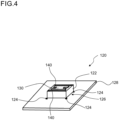
- FIG 4 illustrates, in a highly schematic fashion, a further exemplary detector module 120 according to the present invention.
- the detector module 120 may comprise at least one photosensitive detector 122.
- the photosensitive detector 122 may comprise at least one photosensitive region 130.
- the air gap 126 generating at least one spacer 124, particularly a plurality of spacers 124, may be an adhesive, particularly a thermally insulating adhesive.
- the spacer 124 may be a thermally isolating glue ball.
- the electric conductor 140, specifically the bond wires, for conducting the generated detector signal are separate of the spacer 124.
- the supporting member 128 is a substrate.
- the detector module 120 may be produced by at least one of: anisotropic etching; stacking of materials.
- a computer program comprising instructions which, when the program is executed by the spectrometer device 110 cause the evaluation unit 142 of the spectrometer device 110 to determine at least one item of spectral information about the at least one measurement object 112.
- a computer-readable storage medium comprising instructions which, when the program is executed by the spectrometer device 110 cause the evaluation unit 142 of the spectrometer device 110 to determine at least one item of spectral information about the at least one measurement object 112.
- a non-transient computer-readable medium including instructions that, when executed by one or more processors of an evaluation unit 142 of the spectrometer device 110 one or more processors to determine at least one item of spectral information about the at least one measurement object 112 by considering the detector signal.
Landscapes
- Physics & Mathematics (AREA)
- Spectroscopy & Molecular Physics (AREA)
- General Physics & Mathematics (AREA)
- Biochemistry (AREA)
- Chemical & Material Sciences (AREA)
- Analytical Chemistry (AREA)
- Life Sciences & Earth Sciences (AREA)
- General Health & Medical Sciences (AREA)
- Health & Medical Sciences (AREA)
- Immunology (AREA)
- Pathology (AREA)
- Electromagnetism (AREA)
- Investigating Or Analysing Materials By Optical Means (AREA)
Abstract
The invention relates to a detector module (120) for detecting light (118) and, thereby generating at least one detector signal, wherein the detector module (120) comprises:- at least one photosensitive detector (122) designated for generating at least one detector signal when illuminated by light (118);- at least one spacer (124), wherein the spacer (124) supports the photosensitive detector (122) in manner that at least one thermally insulating air gap (126) is generated between the photosensitive detector (122) and at least one supporting member (128) for thermally decoupling the photosensitive detector (122) from an environment.The invention further relates to a method for producing a detector module (120), a spectrometer device (110), a computer program, a computer-readable storage medium and a non-transient computer-readable medium.
Description
- The invention relates to a detector module for detecting light. The invention further relates to a method for producing a detector module, a spectrometer device, a computer program, a computer-readable storage medium and a non-transient computer-readable medium. Such methods, devices, computer programs and computer-readable media can, in general, be used for investigating and/or monitoring purposes, in particular in the infrared (IR) spectral region, especially in the near-infrared (NIR) and the mid-infrared spectral region. However, further kinds of applications are conceivable.
- In practice, a spectrometer device may be subject to drifting effects which can be caused by variations of a temperature of a detector module comprised by the spectrometer device, resulting in a strong thermal drift in the measurement signal, which makes the analysis of the measurement signal difficult.
- Typically, the detector modules are thermally well connected to a surrounding module. The detector module, therefore, may easily adapt the temperature of the surrounding module, which may increase the drifting effects when the temperature of the surrounding module variates.
- Therefore, the problem addressed by the present invention is that of providing a spectrometer device and a method for determining at least one item of spectral information about at least one measurement object as well as a related computer program and a non-transient computer-readable medium, which at least substantially avoid the disadvantages of known devices and methods of this type.
- In particular, it would be desirous to have a detector module that shows minimized drifting effects. It would further be desirous to have a method for producing a detector module, a spectrometer device, a computer program, a computer-readable storage medium and a non-transient computer-readable medium that further address these problems.
- This problem is solved by the invention with the features of the independent patent claims. Advantageous developments of the invention, which can be implemented individually or in combination, are presented in the dependent claims, in the following specification and in the detailed embodiments.
- In a first aspect of the present invention, a detector module for detecting light, particularly by using a spectrometer device, and, thereby, generating a detector signal is disclosed. The detector module comprises:
- at least one photosensitive detector designated for generating at least one detector signal when illuminated by light;
- at least one spacer, particularly a plurality of spacers, wherein the spacer supports the photosensitive detector in manner that at least one thermally insulating air gap is generated between the photosensitive detector and at least one supporting member for thermally decoupling the photosensitive detector from an environment.
- As already disclosed in the above, the detector module comprises at least one photosensitive detector is designated for generating at least one detector signal when illuminated by light.
- The term "detector module" as used herein is a broad term and is to be given its ordinary and customary meaning to a person of ordinary skill in the art and is not to be limited to a special or customized meaning. The term specifically may refer, without limitation, refers to an arbitrary unit designated for generating at least one detector signal depending on the intensity of the light received by the sensor region. The detector signal may be associated with at least one wavelength range. The at least one detector signal may, in particular, be provided to an evaluation unit for evaluation. Particularly thereby, an item of spectroscopic information on a measurement object may be generated.
- The "detector signal" may be an analogue signal and/or a digital signal. The detector signal may be selected from an electrical current or an electrical voltage; however, using an optical signal as generated by the at least one photosensitive detector may also be feasible. In a particular embodiment, the at least one detector module may be or comprise an active sensor which may be adapted to amplify the electronic signals prior to providing it, for example, to the evaluation unit. For this purpose, the detector module may comprise one or more signal processing devices, in particular one or more filters and/or analogue-digital-converters for processing and/or preprocessing the electronic signals.
- The term "photosensitive detector" as used herein is a broad term and is to be given its ordinary and customary meaning to a person of ordinary skill in the art and is not to be limited to a special or customized meaning. The term specifically may refer, without limitation, refers to an optical detector which may be or may comprise at least one photosensitive region, which particularly is, depending on the illumination of the at least one photosensitive region, designated for generating the at least one detector signal. Typical types of photosensitive detector are photodiodes and/or photoresistors.
- The at least one photosensitive region a may, preferably, be a single, uniform photosensitive area which is configured to receive the emitted light that impinges on the photosensitive area. However, more than one photosensitive area, such as an array of pixel-sized photosensitive areas, may also be feasible.
- The photosensitive region may comprise at least one photoconductive material. The term "photoconductive material" as used herein is a broad term and is to be given its ordinary and customary meaning to a person of ordinary skill in the art and is not to be limited to a special or customized meaning. The term specifically may refer, without limitation, refers to a type of material that exhibits an increase in electrical conductivity when it is exposed to light. A photosensitive region comprising a photoconductive material device may, typically, be connected to a plurality of electrical contacts that are connected to an external circuit, particularly comprising an evaluation unit. When light is incident on the photoconductive material, it may generate free charge carriers, such as electrons and/or holes, which may increase the electrical conductivity of the material. This change in conductivity may be observed by the external circuit as an electrical signal, which may, as an example, be fed to the evaluation unit.
- The photoconductive material may be or may comprise at least one inorganic photoconductive material. The photoconductive material may be or may comprise at least one of:
- lead sulfide (PbS);
- lead selenide (PbSe);
- germanium (Ge);
- indium gallium arsenide (InGaAs);
- indium antimonide (InSb);
- mercury cadmium telluride (HgCdTe or MCT).
- Particularly lead sulfide (PbS) and/or lead selenide (PbSe) show a strong temperature drift characteristic. Photosensitive detectors comprising these materials thereby advantageously benefit from the invention disclosed herein.
- The term "light" as used herein is a broad term and is to be given its ordinary and customary meaning to a person of ordinary skill in the art and is not to be limited to a special or customized meaning. The term specifically may refer, without limitation, to electromagnetic radiation. Light may be formed by at least one electromagnetic field wave and or at least one particle. Visible light may, usually, be defined as having a wavelength in a range of 380 to 760 nm, between the infrared and the ultraviolet. Infrared light may, typically, be defined as having a wavelength in a range above 760 nm to 1 mm.
- As already disclosed in the above, the detector module comprises at least one spacer, wherein the spacer supports the photosensitive detector in manner that at least one thermally insulating air gap is generated between the photosensitive detector and at least one supporting member for thermally decoupling the photosensitive detector from an environment.
- The term "spacer" as used herein is a broad term and is to be given its ordinary and customary meaning to a person of ordinary skill in the art and is not to be limited to a special or customized meaning. The term specifically may refer, without limitation, to at least one device and/or at least one material being used to create and/or preserve a space between a plurality of objects and/or surfaces. By using the spacer, the plurality of objects is separated in a manner that the objects to not contact each other. In particular accordance with the present invention, the space may be used to separate the photosensitive detector from the supporting member. Thus, the photosensitive detector and the supporting member may be separated from each other, particularly by the spacer. Thereby, a space, particularly an air gap, is generated. As an example, the photosensitive detector may be fully surrounded by air and only the spacer, particularly used as an electrical contact for providing the detector signal, may contact the photosensitive detector. In addition, a separate electrical contact may further contact the photosensitive detector.
- The term "supporting member" as used herein is a broad term and is to be given its ordinary and customary meaning to a person of ordinary skill in the art and is not to be limited to a special or customized meaning. The term specifically may refer, without limitation, to at least one structural element that is designed for bearing loads and/or provide support to at least one further structural element. In particular accordance with the present invention, the supporting element carries the spacer in a manner that the photosensitive detector is mounted at a distance from the supporting member. By mounting the photosensitive detector in a distance from the supporting member an air gap is generated. The supporting member may comprise a surface for placing the spacer.
- The photosensitive detector and/or the supporting member may be plate-like. The term "plate-like" as used herein is a broad term and is to be given its ordinary and customary meaning to a person of ordinary skill in the art and is not to be limited to a special or customized meaning. The term specifically may refer, without limitation, to an object that may be, typically, thin and/or flat with a shape that is wider than it is thick. Particularly then, the photosensitive detector and the supporting member may be parallel, particularly with a maximum deviation thereof of 5°, 4°, 3°, 2°, 1° or 0.5°. A distance between the photosensitive detector and the supporting member generated by the thermally insulating air gap may be between 1 µm and 1 mm, preferably ... , even more preferably....
- The supporting member may be a substrate, particularly comprised by the detector module. The term "substrate" as used herein is a broad term and is to be given its ordinary and customary meaning to a person of ordinary skill in the art and is not to be limited to a special or customized meaning. The term specifically may refer, without limitation, to a material, typically a board and/or a wafer, that may be flat and/or board, on which at least one electronic component is attached. The substrate may provide a physical support structure for the at least one component. Alternatively or in addition, the substrate may also serve as a medium for the transfer of electrical signals.
- The spacer may be or may comprise an electric conductor for conducting the generated detector signal. The term "electrical conductor" as used herein is a broad term and is to be given its ordinary and customary meaning to a person of ordinary skill in the art and is not to be limited to a special or customized meaning. The term specifically may refer, without limitation, to a material that allows electrical charges to flow through it. The electrical conductor may have a high density of free electrons, which then may move easily through the material in response to an electric field. The electric conductor may be at least one of: a bond wire, particularly comprising a metal; a bond pad, particularly comprising a metal. The "bond wire" may be a thin wire used to make an electrical connection between a plurality of points in a circuit. A bond wire may be, typically, comprise a metal, such as gold, aluminum and/or copper. A diameter of a bond wire may be less than 1 mm in diameter. The "bond pad" may be a small area that is designed to be used for wire bonding. Bond pads may, typically, be made of a metal, such as aluminum, gold and/or copper.
- The thermal conductivity of the spacer thermally connecting the photosensitive detector and the supporting member may be below 0.1 W/(mK) (Watt per meter/Kelvin). The term "thermal conductivity" as used herein is a broad term and is to be given its ordinary and customary meaning to a person of ordinary skill in the art and is not to be limited to a special or customized meaning. The term specifically may refer, without limitation, to a measure of a material's ability to conduct heat. In particular accordance with the present invention, the thermal conductivity may refer to ability of the spacer to conduct heat, wherein the spacer acts as a medium for the transfer of heat between the photosensitive detector and the supporting member. The spacer may be or may comprise at least one thermally insulating material. A material may be considered as thermally insulating, when the thermal conductivity of the material may be below 0.1 W/(mK )(Watt per meter/Kelvin).
- The thermally insulating material may be an adhesive. The term "adhesive" as used herein is a broad term and is to be given its ordinary and customary meaning to a person of ordinary skill in the art and is not to be limited to a special or customized meaning. The term specifically may refer, without limitation, to a substance that is used to bond at least two surfaces of respective objects together by creating a permanent and/or temporary bond. The adhesive may be and/or may comprise at least one of: epoxy, acrylic, silicone, polyurethane, cyanoacrylate.
- For the detector module, reference may be made to any further aspect, Embodiment and/or definition as disclosed elsewhere herein.
- In a further aspect of the present invention, a method for producing a detector module is disclosed. According to this method, a detector module as described elsewhere herein is produced by anisotropic etching; and/or stacking of materials. For the method for producing a detector module, reference may be made to any further aspect, Embodiment and/or definition as disclosed elsewhere herein.
- The term "anisotropic etching" as used herein is a broad term and is to be given its ordinary and customary meaning to a person of ordinary skill in the art and is not to be limited to a special or customized meaning. The term specifically may refer, without limitation, to a type of an etching process in which material is selectively removed from a substrate, particularly in a non-uniform manner. Anisotropic etching may result in the formation of complex three-dimensional structures.
- The term "stacking of material" as used herein is a broad term and is to be given its ordinary and customary meaning to a person of ordinary skill in the art and is not to be limited to a special or customized meaning. The term specifically may refer, without limitation, to a process of layering and/or stacking a plurality layers of the materials on top of each other, particularly for creating a composite structure.
- In a further aspect of the present invention, a spectrometer device for determining at least one item of spectral information about at least one measurement object is disclosed. The spectrometer device comprising:
- at least one detector module as described elsewhere herein, wherein the at least one detector module is designated for receiving light from the at least one measurement object and, thereby, generating at least one detector signal;
- at least one evaluation unit, wherein the at least one evaluation unit is configured to determine at least one item of spectral information about the at least one measurement object by considering the detector signal.
- For the spectrometer device, reference may be made to any further aspect, Embodiment and/or definition as disclosed elsewhere herein.
- The term "measurement object", generally, refers to an arbitrary body, chosen from a living object and a non-living object, which comprises material for investigation by the spectrometer device. The term "spectrometer device" as used herein is a broad term and is to be given its ordinary and customary meaning to a person of ordinary skill in the art and is not to be limited to a special or customized meaning. The term specifically may refer, without limitation, to an apparatus which is configured to determine at least one item of spectral information spectral information. As generally used, the term "determining" or any grammatical variation thereof refers to a process of generating at least one representative result, in particular, by evaluating the at least one detector signal as acquired by the at least one photosensitive detector. The term "evaluating" or any grammatical variation thereof refers to an application of methods for deriving the at least one representative result from the at least one detector signal. As generally used, the term "spectral information" refers to at least one measured value which is obtained by recording at least one signal intensity related to at least one corresponding signal wavelength of the optical radiation and evaluating at least one detector signal which relates to the signal intensity.
- The term "evaluation unit" as used herein is a broad term and is to be given its ordinary and customary meaning to a person of ordinary skill in the art and is not to be limited to a special or customized meaning. The term specifically may refer, without limitation, to an arbitrary device designed to generate the at least one desired item of information, in particular related to the spectrum of the object. For this purpose, the evaluation unit may be or may comprise one or more integrated circuits, such as one or more application-specific integrated circuits (ASICs), and/or one or more data processing devices, such as one or more of computers, digital signal processors (DSP), field programmable gate arrays (FPGA) preferably one or more microcomputers and/or microcontrollers, especially comprised by at least one mobile communication device, in particular selected from a smartphone, a tablet or a laptop; however further embodiments may also be feasible. Additional components may be comprised, such as one or more preprocessing devices and/or data acquisition devices, such as one or more devices for receiving and/or preprocessing of the detector signals, such as one or more AD-converters and/or one or more filters. As used herein, the detector signal is provided by the spectrometer device, in particular, by the detector array of the spectrometer device. Further, the evaluation unit may comprise one or more data storage devices. Further, the evaluation unit may comprise one or more interfaces, such as one or more wireless interfaces and/or one or more wire-bound interfaces.
- The spectrometer device may, preferably, be configured to determine the at least one item of spectral information about at least one measurement object by spectrally analyzing the optical radiation which the at least one photosensitive detector may receive from the at least one measurement object. The spectrometer device may, preferably, be configured to determine the at least one item of spectral information about at least one measurement object by spectrally analyzing diffuse reflected optical radiation as generated by the at least one measurement object and directed towards the at least one photosensitive detector.
- In a further aspect of the present invention, a computer program comprising instructions which, when the program is executed by the spectrometer device as described elsewhere herein, cause the evaluation unit of the spectrometer device to determine at least one item of spectral information about the at least one measurement object. For the computer program, reference may be made to any further aspect, Embodiment and/or definition as disclosed elsewhere herein.
- Specifically, the computer program may be stored on a computer-readable data carrier and/or on a computer-readable storage medium. The computer program may be executed on at least one processor comprised by the spectrometer device.
- In a further aspect of the present invention, a computer-readable storage medium is disclosed, wherein the computer-readable storage medium comprises instructions, which, when the program is executed by the spectrometer device as described elsewhere herein cause the evaluation unit of the spectrometer device to determine at least one item of spectral information about the at least one measurement object. For the computer-readable storage medium, reference may be made to any further aspect, Embodiment and/or definition as disclosed elsewhere herein.
- As used herein, the terms "computer-readable data carrier" and "computer-readable storage medium" specifically may refer to non-transitory data storage means, such as a hardware storage medium having stored thereon computer-executable instructions. The stored computer-executable instruction may be associate with the computer program. The computer-readable data carrier or storage medium specifically may be or may comprise a storage medium such as a random-access memory (RAM) and/or a read-only memory (ROM).
- In a further aspect of the present invention, a non-transient computer-readable medium is disclosed, wherein the non-transient computer-readable medium includes instructions that, when executed by one or more processors of an evaluation unit of a spectrometer device as described elsewhere herein cause one or more processors to determine at least one item of spectral information about the at least one measurement object by considering a detector signal. For the non-transient computer-readable medium, reference may be made to any further aspect, Embodiment and/or definition as disclosed elsewhere herein.
- To avoid limit the disturbing effect of the temperature drift seen in the previous chapter, the PbS pixels can be thermally isolated. This is achieved by reducing the thermal connections from the active measurement area to the surrounding environment.
- As used herein, the terms "have", "comprise" or "include" or any arbitrary grammatical variations thereof are used in a non-exclusive way. Thus, these terms may both refer to a situation in which, besides the feature introduced by these terms, no further features are present in the entity described in this context and to a situation in which one or more further features are present. As an example, the expressions "A has B", "A comprises B" and "A includes B" may both refer to a situation in which, besides B, no other element is present in A (i.e. a situation in which A solely and exclusively consists of B) and to a situation in which, besides B, one or more further elements are present in entity A, such as element C, elements C and D or even further elements.
- Further, it shall be noted that the terms "at least one", "one or more" or similar expressions indicating that a feature or element may be present once or more than once typically are used only once when introducing the respective feature or element. In most cases, when referring to the respective feature or element, the expressions "at least one" or "one or more" are not repeated, nonwithstanding the fact that the respective feature or element may be present once or more than once.
- Further, as used herein, the terms "preferably", "more preferably", "particularly", "more particularly", "specifically", "more specifically" or similar terms are used in conjunction with optional features, without restricting alternative possibilities. Thus, features introduced by these terms are optional features and are not intended to restrict the scope of the claims in any way. The invention may, as the skilled person will recognize, be performed by using alternative features. Similarly, features introduced by "in an embodiment of the invention" or similar expressions are intended to be optional features, without any restriction regarding alternative embodiments of the invention, without any restrictions regarding the scope of the invention and without any restriction regarding the possibility of combining the features introduced in such way with other optional or non-optional features of the invention.
- The spectrometer device and the method according to the present invention, in one or more of the above-mentioned embodiments and/or in one or more of the embodiments described in further detail below, provide a large number of advantages over known devices and methods of similar kind. The present invention particularly provides a detector module that shows minimized drifting effects.
- The minimized drifting effects may be made possible by using Micro-Electro-Mechanical Systems (MEMS) technology for generating a micro-bridge style setup that may be used to thermally isolate the detector module, particularly by generating an air gap between the detector module and a supporting member. Since air has a significantly lower thermal conductance than glass or silicon substrate, a thermal transfer to the system, particularly the detector module, from an environment, particularly a light source comprised by the spectrometer device, may significantly be reduced in a manner that unwanted heat-up effects are suppressed.
- Summarizing, in the context of the present invention, the following embodiments are regarded as preferred:
- Embodiment 1. A detector module for detecting light, particularly by using a spectrometer device, and, thereby, generating at least one detector signal, the detector module comprises:
- at least one photosensitive detector designated for generating at least one detector signal when illuminated by light;
- at least one spacer, wherein the spacer supports the photosensitive detector in manner that at least one thermally insulating air gap is generated between the photosensitive detector and at least one supporting member for thermally decoupling the photosensitive detector from an environment.
- Embodiment 2. The detector module according to the preceding embodiment, wherein the photosensitive detector is or comprises at least one photosensitive region.
- Embodiment 3. The detector module according to the preceding embodiment, wherein the photosensitive region comprises at least one photoconductive material.
- Embodiment 4. The detector module according to the preceding embodiment, wherein the photoconductive material is or comprises at least one inorganic photoconductive material.
- Embodiment 5. The detector module according to any one of the two preceding embodiments, wherein the photoconductive material is or comprises at least one of:
- lead sulfide (PbS);
- lead selenide (PbSe);
- germanium (Ge);
- indium gallium arsenide (InGaAs);
- indium antimonide (InSb);
- mercury cadmium telluride (HgCdTe or MCT).
- Embodiment 6. The detector module according to any one of the preceding embodiments, wherein the photosensitive detector and supporting member are parallel with a maximum deviation thereof of 5°, 4°, 3°, 2°, 1° or 0.5°.
- Embodiment 7. The detector module according to any one of the preceding embodiments, wherein a distance between the photosensitive detector and the supporting member generated by the thermally insulating air gap is between 1 µm and 1 mm.
- Embodiment 8. The detector module according to any one of the preceding embodiments, wherein the photosensitive detector and the supporting member are separated from each other, particularly by the spacer.
- Embodiment 9. The detector module according to any one of the preceding embodiments, wherein the supporting member is a substrate, particularly comprised by the detector module.
- Embodiment 10. The detector module according to any one of the preceding embodiments, wherein the supporting member comprises a surface for placing the spacer.
- Embodiment 11. The detector module according to the preceding embodiment, wherein the spacer is or comprises an electric conductor for conducting the generated detector signal.
- Embodiment 12. The detector module according to the preceding embodiment, wherein the electric conductor is at least one of:
- bond wire, particularly comprising a metal;
- bond pad, particularly comprising a metal.
- Embodiment 13. The detector module according to the preceding embodiment, wherein the spacer is or comprises at least one thermally insulating material.
- Embodiment 14. The detector module according to the preceding embodiment, wherein the thermally insulating material is an adhesive.
- Embodiment 15. A method for producing a detector module, wherein a detector module according to any one of the preceding embodiments referring to a detector module is produced by at least one of:
- anisotropic etching;
- stacking of materials.
- Embodiment 16. A spectrometer device for determining at least one item of spectral information about at least one measurement object, the spectrometer device comprising:
- at least one detector module according to any one of the preceding embodiments referring to a detector module, wherein the at least one detector module is designated for receiving light from the at least one measurement object and, thereby, generating at least one detector signal;
- at least one evaluation unit, wherein the at least one evaluation unit is configured to determine at least one item of spectral information about the at least one measurement object by considering the detector signal.
- Embodiment 17. A computer program comprising instructions which, when the program is executed by the spectrometer device according to any one of the preceding embodiments referring to a spectrometer device cause the evaluation unit of the spectrometer device to determine at least one item of spectral information about the at least one measurement object.
- Embodiment 18. A computer-readable storage medium comprising instructions which, when the program is executed by the spectrometer device according to any one of the preceding embodiments referring to a spectrometer device cause the evaluation unit of the spectrometer device to determine at least one item of spectral information about the at least one measurement object.
- Embodiment 19. A non-transient computer-readable medium including instructions that, when executed by one or more processors of an evaluation unit of a spectrometer device according to any one of the preceding embodiments referring to a spectrometer device cause one or more processors to determine at least one item of spectral information about the at least one measurement object by considering a detector signal.
- Further optional details and features of the invention are evident from the description of preferred exemplary embodiments which follows in conjunction with the dependent Embodiments. In this context, the particular features may be implemented alone or in any reasonable combination. The invention is not restricted to the exemplary embodiments. The exemplary embodiments are shown schematically in the figures. Identical reference numerals in the individual figures refer to identical elements or elements with identical function, or elements which correspond to one another with regard to their functions. In the Figures:
- Figure 1
- shows a typical drifting effect of a spectrometer device from the prior art;
- Figure 2
- shows an exemplary spectrometer device;
- Figure 3a-3b
- show a further exemplary detector module; and
- Figure 4
- shows a further exemplary detector module.
-
Figure 1 illustrates a typical temperature drifting effect over time which is caused by a self-heating of a detector module comprised by a spectrometer device. On thehorizontal axis 100 the consecutive time frames of the spectrometer device are depicted. On thevertical axis 102 thesignal intensity different signal intensities signal intensity 104 is associated with a strong temperature drift, thesignal intensity 106 is associated with a medium temperature drift of approximately 1 K/s and thesignal intensity 108 is associated with a small temperature drift. As may be derived fromFigure 1 , different temperature drifts make the analysis of the measurement signal difficult. The present invention mitigates this problem by significantly reducing the temperature drifts. With thermal isolation, the signal drift is expected to be significantly reduced and the following light intensity analysis of higher quality. -
Figure 2 illustrates, in a highly schematic fashion, anexemplary spectrometer device 110 according to the present invention. Thespectrometer device 110 is an apparatus which is configured to determine at least one item of spectral information about at least onemeasurement object 112. Themeasurement object 112 may be or comprise an arbitrary body, chosen from a living object and a non-living object, which comprises material for investigation or monitoring by thespectrometer device 110. - According to the present invention, the
spectrometer device 110 may be adapted for recording a spectrum, particularly in the infrared (IR) spectral region, especially in the near-infrared (NIR), specifically for a wavelength of 760 nm to 3 µm, preferably of 1 µm to 5 µm, more preferred of 1 µm to 3 µm, or in the mid-infrared spectral region which covers wavelengths from 5 µm to 15 µm. Accordingly, thespectrometer device 110 can be used for monitoring or investigation purposes, such as spectroscopy, gas sensing, or concentration measurements. However, further applications of thespectrometer device 110 may also be feasible. - As depicted in
Figure 2 , thespectrometer device 110 may comprise ahousing 114 which encompasses the components of thespectrometer device 110. In this fashion, the components of thespectrometer device 110 can be protected and access of external light may be impeded. Further, thehousing 114 can, preferably, be filled with an optically transparent medium, wherein the opticallytransparent medium 134 may, especially, be selected from ambient air, an inert gas or vacuum, especially in order to facilitate a propagation of the light beam within thehousing 114. However, different kind of materials may also be feasible. However, further kinds of arrangements of the components of thespectrometer device 110 may also be conceivable. - The
exemplary spectrometer device 110 as schematically depicted inFigure 1 may comprise aradiation emitting element 116 which is configured to emit the light 118. Herein, theradiation emitting element 116 may comprise by a semiconductor-based radiation source, preferably, selected from at least one of a light emitting diode (LED) or a laser, in particular a laser diode. However, a further type ofradiation emitting element 116 may also be feasible. Theradiation emitting element 116 may be continuously emitting, or generating modulated optical pulses, as described above in more detail. Theradiation emitting element 116 may be configured for emitting the light 118 isotropically in all spatial directions. However, theradiation emitting element 116 may, preferably, be designed for emitting the light 118 anisotropically in at least one spatial direction, specifically towards the at least onemeasurement object 112, such as by generating at least one light beam. - The
exemplary spectrometer device 110 as illustrated inFigure 2 , further, may comprise anoptical window 136. The at least one window 136may be at least partially, preferably fully, transparent for the light 118. Herein, at least one transparent material as comprised by theoptical window 136 may, preferably, be selected from glass or silicon and may, therefore, preferably be at least partially, preferably fully, transparent in at least a partition of a wavelength range covered by the light 118. Theoptical window 136 may, especially be located in a portion of thehousing 114 of thespectrometer device 110, specifically in a portion of a beam path of the light 118 between theradiation emitting element 116 and the at least onemeasurement object 112 and, further, in a further portion of the beam path of theoptical radiation 118 between the at least onemeasurement object 112 and at least onedetector module 120. - As further schematically illustrated in
Figure 2 , thespectrometer device 110 may, further, comprise afilter element 138, such as a polarization filter element or a bandpass filter element, however, a further kind offilter element 138 may also be feasible. Thefilter element 138 may, especially, be designed for filtering the light 118 or, more specifically, selected wavelengths of the light 118. For this purpose, thefilter element 138 may, specifically, be positioned in the beam path of the light 118 in front of thedetector module 120. In further embodiments (not depicted here), thefilter element 138 may also be dispensable. - Further, the
exemplary spectrometer device 110 as schematically illustrated inFigure 1 comprises adetector module 120 for detecting light and, thereby, generating at least one detector signal. The detector module comprises: - at least one
photosensitive detector 122 designated for generating at least one detector signal when illuminated by light; - at least one
spacer 124, wherein the spacer supports thephotosensitive detector 122 in manner that at least one thermally insulatingair gap 126 is generated between thephotosensitive detector 122 and at least one supportingmember 128 for thermally decoupling the photosensitive detector from an environment. - The
photosensitive detector 122 may comprise at least onephotosensitive region 130, which may comprise at least one photoconductive material. Alternatively, thephotosensitive detector 122 may be the at least onephotosensitive region 130, particularly in a manner that the entirephotosensitive detector 122 is the at least onephotosensitive region 130. - The photoconductive material may be or may comprise at least one inorganic photoconductive material. The photoconductive material may be or may comprise at least one of:
- lead sulfide (PbS);
- lead selenide (PbSe);
- germanium (Ge);
- indium gallium arsenide (InGaAs);
- indium antimonide (InSb);
- mercury cadmium telluride (HgCdTe or MCT).
- As may be derived from
Fig. 1 , thephotosensitive detector 122 and supportingmember 128 may be parallel with a maximum deviation thereof of 5°, 4°, 3°, 2°, 1° or 0.5°. Thephotosensitive detector 122 and supportingmember 128 may be parallel in a manner that acentral axis 132 of thephotosensitive detector 122 and acentral axis 134 of the supportingmember 128 may be parallel. - The
photosensitive detector 120 and the supportingmember 128 are separated from each other, particularly by thespacer 126 that is generating theair gap 126. The supportingmember 128 may be a substrate, particularly comprised by thedetector module 120. The supportingmember 128 comprises a surface for placing thespacer 126. The spacer may be or may comprise at least one thermally insulating material. A typical distance between the photosensitive detector and the supporting member generated by the thermally insulating air gap may be between 1 µm and 1 mm. - The
exemplary spectrometer device 110 as schematically illustrated inFigure 1 further comprises at least one evaluation unit 142, wherein the at least one evaluation unit 142 is configured to determine at least one item of spectral information about the at least onemeasurement object 112 by considering the detector signal. -
Figure 3a illustrates, in a highly schematic fashion, a top view on anexemplary detector module 120 according to the present invention.Figure 3b illustrates a cross section of theexemplary detector module 120 ofFigure 3a at the interface A-A. Thedetector module 120 comprises at least onephotosensitive detector 122. Thephotosensitive detector 122 may be at least onephotosensitive region 130 comprising photoconductive material. The photoconductive material may be lead sulfide (PbS). - The
detector module 120 comprises at least one, particularly a plurality ofspacers 124, that support thephotosensitive detector 122 in manner that at least one thermally insulatingair gap 126 is generated between thephotosensitive detector 122 and at least one supportingmember 128 for thermally decoupling the photosensitive detector from an environment. The spacer may be an electric conductor for conducting the generated detector signal. Alternatively, the spacer may comprise an electric conductor (not depicted). The electric conductor may be a bond wire, particularly comprising a metal. Alternatively, thespacer 124 may be a bond pad, particularly comprising a metal (not depicted). The supportingmember 128 is a substrate. The substrate is a silicon substrate or glass substrate. -
Figure 4 illustrates, in a highly schematic fashion, a furtherexemplary detector module 120 according to the present invention. Thedetector module 120 may comprise at least onephotosensitive detector 122. Thephotosensitive detector 122 may comprise at least onephotosensitive region 130. Theair gap 126 generating at least onespacer 124, particularly a plurality ofspacers 124, may be an adhesive, particularly a thermally insulating adhesive. Thespacer 124 may be a thermally isolating glue ball. Theelectric conductor 140, specifically the bond wires, for conducting the generated detector signal are separate of thespacer 124. The supportingmember 128 is a substrate. - The
detector module 120 may be produced by at least one of: anisotropic etching; stacking of materials. - Further disclosed herein is, a computer program comprising instructions which, when the program is executed by the
spectrometer device 110 cause the evaluation unit 142 of thespectrometer device 110 to determine at least one item of spectral information about the at least onemeasurement object 112. - Further disclosed herein is, a computer-readable storage medium comprising instructions which, when the program is executed by the
spectrometer device 110 cause the evaluation unit 142 of thespectrometer device 110 to determine at least one item of spectral information about the at least onemeasurement object 112. - Further disclosed herein is, a non-transient computer-readable medium including instructions that, when executed by one or more processors of an evaluation unit 142 of the
spectrometer device 110 one or more processors to determine at least one item of spectral information about the at least onemeasurement object 112 by considering the detector signal. -
- 100
- horizontal axis
- 102
- vertical axis
- 104
- signal intensity
- 106
- signal intensity
- 108
- signal intensity
- 110
- spectrometer device
- 112
- measurement object
- 114
- housing
- 116
- radiation emitting element
- 118
- light
- 120
- detector module
- 122
- photosensitive detector
- 124
- spacer
- 126
- air gap
- 128
- supporting member
- 130
- photosensitive region
- 132
- central axis of the photosensitive detector
- 134
- central axis of the supporting member
- 136
- optical window
- 138
- filter element
- 140
- separate electric conductor
- 142
- evaluation unit
Claims (15)
- A detector module (120) for detecting light (118) and, thereby generating at least one detector signal, the detector module (120) comprises:- at least one photosensitive detector (122) designated for generating at least one detector signal when illuminated by light (118);- at least one spacer (124), wherein the spacer (124) supports the photosensitive detector (122) in manner that at least one thermally insulating air gap (126) is generated between the photosensitive detector (122) and at least one supporting member (128) for thermally decoupling the photosensitive detector (122) from an environment.
- The detector module (120) according to the preceding claim, wherein the photosensitive detector (122) is or comprises at least one photosensitive region (130), wherein the photosensitive region (130) comprises at least one photoconductive material.
- The detector module (120) according to any one of the two preceding claims, wherein the photoconductive material is or comprises at least one of:- lead sulfide;- lead selenide;- germanium;- indium gallium arsenide;- indium antimonide;- mercury cadmium telluride.
- The detector module (120) according to any one of the preceding claims, wherein the photosensitive detector (122) and the supporting member (128) are separated from each other by the spacer (124).
- The detector module (120) according to any one of the preceding claims, wherein the supporting member (128) is a substrate.
- The detector module (120) according to any one of the preceding claims, wherein the supporting member (128) comprises a surface for placing the spacer (124).
- The detector module (120) according to the preceding claim, wherein the spacer (124) is or comprises an electric conductor for conducting the generated detector signal.
- The detector module (120) according to the preceding claim, wherein the electric conductor is at least one of:- bond wire;- bond pad.
- The detector module (120) according to the preceding claim, wherein the spacer (124) is or comprises at least one thermally insulating material.
- The detector module (120) according to the preceding claim, wherein the thermally insulating material is an adhesive.
- A method for producing a detector module (120), wherein a detector module (120) according to any one of the preceding claims referring to a detector module (120) is produced by at least one of:- anisotropic etching;- stacking of materials.
- A spectrometer device (110) for determining at least one item of spectral information about at least one measurement object (112), the spectrometer device (110) comprising:- at least one detector module (120) according to any one of the preceding claims referring to a detector module (120), wherein the at least one detector module (120) is designated for receiving light (118) from the at least one measurement object (112) and, thereby, generating at least one detector signal;- at least one evaluation unit (142), wherein the at least one evaluation unit (142) is configured to determine at least one item of spectral information about the at least one measurement object (112) by considering the detector signal.
- A computer program comprising instructions which, when the program is executed by the spectrometer device (110) according to any one of the preceding claims referring to a spectrometer device (110) cause the evaluation unit (142) of the spectrometer device (110) to determine at least one item of spectral information about the at least one measurement object (112).
- A computer-readable storage medium comprising instructions which, when the program is executed by the spectrometer device (110) according to any one of the preceding claims referring to a spectrometer device (110) cause the evaluation unit (142) of the spectrometer device (110) to determine at least one item of spectral information about the at least one measurement object (112).
- A non-transient computer-readable medium including instructions that, when executed by one or more processors of an evaluation unit (142) of a spectrometer device (110) according to any one of the preceding claims referring to a spectrometer device (110) cause one or more processors to determine at least one item of spectral information about the at least one measurement object (112) by considering a detector signal.
Priority Applications (1)
| Application Number | Priority Date | Filing Date | Title |
|---|---|---|---|
| EP23168772.4A EP4450933A1 (en) | 2023-04-19 | 2023-04-19 | Thermally decoupled photosensitive detector |
Applications Claiming Priority (1)
| Application Number | Priority Date | Filing Date | Title |
|---|---|---|---|
| EP23168772.4A EP4450933A1 (en) | 2023-04-19 | 2023-04-19 | Thermally decoupled photosensitive detector |
Publications (1)
| Publication Number | Publication Date |
|---|---|
| EP4450933A1 true EP4450933A1 (en) | 2024-10-23 |
Family
ID=86095733
Family Applications (1)
| Application Number | Title | Priority Date | Filing Date |
|---|---|---|---|
| EP23168772.4A Withdrawn EP4450933A1 (en) | 2023-04-19 | 2023-04-19 | Thermally decoupled photosensitive detector |
Country Status (1)
| Country | Link |
|---|---|
| EP (1) | EP4450933A1 (en) |
Citations (3)
| Publication number | Priority date | Publication date | Assignee | Title |
|---|---|---|---|---|
| US20090140148A1 (en) * | 2007-11-29 | 2009-06-04 | Electronics And Telecommunications Research Institute | Bolometer and method of manufacturing the same |
| US20100171097A1 (en) * | 2009-01-05 | 2010-07-08 | Sumitomo Electric Industries, Ltd. | Detection device and method for manufacturing the same |
| EP2337082A2 (en) * | 2009-12-17 | 2011-06-22 | Raytheon | Multi-band, reduced-volume radiation detectors and methods of formation |
-
2023
- 2023-04-19 EP EP23168772.4A patent/EP4450933A1/en not_active Withdrawn
Patent Citations (3)
| Publication number | Priority date | Publication date | Assignee | Title |
|---|---|---|---|---|
| US20090140148A1 (en) * | 2007-11-29 | 2009-06-04 | Electronics And Telecommunications Research Institute | Bolometer and method of manufacturing the same |
| US20100171097A1 (en) * | 2009-01-05 | 2010-07-08 | Sumitomo Electric Industries, Ltd. | Detection device and method for manufacturing the same |
| EP2337082A2 (en) * | 2009-12-17 | 2011-06-22 | Raytheon | Multi-band, reduced-volume radiation detectors and methods of formation |
Non-Patent Citations (2)
| Title |
|---|
| MASAYUKI ABE: "Modulation-Doped Heterostructure-Thermopiles for Uncooled Infrared Image-Sensor Application", IEICE TRANSACTIONS ON ELECTRONICS, INSTITUTE OF ELECTRONICS, TOKYO, JP, vol. E93C, no. 8, 1 August 2010 (2010-08-01), pages 1302 - 1308, XP001558284, ISSN: 0916-8524, DOI: 10.1587/TRANSELE.E93.C.1302 * |
| ROY SANGITA CHAKI ET AL: "Polymer-Based MEMS Photodetector With Spectral Response in UV-Vis-NIR and Mid-IR Region", JOURNAL OF LIGHTWAVE TECHNOLOGY, IEEE, USA, vol. 33, no. 15, 1 August 2015 (2015-08-01), pages 3345 - 3350, XP011585903, ISSN: 0733-8724, [retrieved on 20150626], DOI: 10.1109/JLT.2015.2430618 * |
Similar Documents
| Publication | Publication Date | Title |
|---|---|---|
| CN1104634C (en) | Thermopile sensor and radiation thermometer with a thermopile sensor | |
| EP2063238B1 (en) | Spectroscope | |
| EP3428589B1 (en) | Light detection device | |
| US10444076B2 (en) | Infrared device | |
| CN109341854B (en) | Optical splitter and method for manufacturing optical splitter | |
| US11725990B2 (en) | Thermographic sensor with thermo-couples on a suspended grid and processing circuits in frames thereof | |
| EP3546902B1 (en) | Multispectral sensor and method for multispectral light sensing | |
| US20180238735A1 (en) | Spatially variable light source and spatially variable detector systems and methods | |
| CN106796146B (en) | Determining the spectral emission characteristics of incident radiation | |
| JP5636557B2 (en) | Infrared sensor manufacturing method, infrared sensor, and quantum infrared gas concentration meter | |
| US20210164836A1 (en) | Spectrometer Device and Method for Producing a Spectrometer Device | |
| CN102914372A (en) | Infrared detecting element and electronic device | |
| KR20210002555A (en) | Dark reference bolometer per pixel | |
| CN115135989B (en) | Methods and systems for broadband optical reflectance spectroscopy | |
| US20140097343A1 (en) | Spectroscopic Detector And Corresponding Method | |
| EP3570325B1 (en) | Infrared sensor substrate and infrared sensor device | |
| JP6476634B2 (en) | Optical receiver module | |
| JP2016163125A (en) | Solid-state imaging device | |
| JP2008524569A (en) | Interferometric detector and camera | |
| US9998688B2 (en) | Thermal imaging device and a method for using same | |
| Sesek et al. | A microbolometer system for radiation detection in the THz frequency range with a resonating cavity fabricated in the CMOS technology | |
| FR3041151A1 (en) | MICROELECTRONIC DEVICE AND METHOD FOR MANUFACTURING THE SAME | |
| US20250067598A1 (en) | Method of manufacturing a spectrometer device | |
| Perenzoni et al. | A monolithic visible, infrared and terahertz 2D detector | |
| KR20180061994A (en) | Multi gas sensing package |
Legal Events
| Date | Code | Title | Description |
|---|---|---|---|
| PUAI | Public reference made under article 153(3) epc to a published international application that has entered the european phase |
Free format text: ORIGINAL CODE: 0009012 |
|
| STAA | Information on the status of an ep patent application or granted ep patent |
Free format text: STATUS: THE APPLICATION HAS BEEN PUBLISHED |
|
| AK | Designated contracting states |
Kind code of ref document: A1 Designated state(s): AL AT BE BG CH CY CZ DE DK EE ES FI FR GB GR HR HU IE IS IT LI LT LU LV MC ME MK MT NL NO PL PT RO RS SE SI SK SM TR |
|
| STAA | Information on the status of an ep patent application or granted ep patent |
Free format text: STATUS: THE APPLICATION HAS BEEN WITHDRAWN |
|
| 18W | Application withdrawn |
Effective date: 20241031 |