EP4449917A2 - Heating body assembly and preparation method therefor, atomizer and electronic atomization device - Google Patents
Heating body assembly and preparation method therefor, atomizer and electronic atomization device Download PDFInfo
- Publication number
- EP4449917A2 EP4449917A2 EP21927686.2A EP21927686A EP4449917A2 EP 4449917 A2 EP4449917 A2 EP 4449917A2 EP 21927686 A EP21927686 A EP 21927686A EP 4449917 A2 EP4449917 A2 EP 4449917A2
- Authority
- EP
- European Patent Office
- Prior art keywords
- electrode
- micropore
- conductive connection
- film
- sub
- Prior art date
- Legal status (The legal status is an assumption and is not a legal conclusion. Google has not performed a legal analysis and makes no representation as to the accuracy of the status listed.)
- Pending
Links
Images



Classifications
-
- A—HUMAN NECESSITIES
- A24—TOBACCO; CIGARS; CIGARETTES; SIMULATED SMOKING DEVICES; SMOKERS' REQUISITES
- A24F—SMOKERS' REQUISITES; MATCH BOXES; SIMULATED SMOKING DEVICES
- A24F40/00—Electrically operated smoking devices; Component parts thereof; Manufacture thereof; Maintenance or testing thereof; Charging means specially adapted therefor
- A24F40/40—Constructional details, e.g. connection of cartridges and battery parts
- A24F40/46—Shape or structure of electric heating means
-
- H—ELECTRICITY
- H05—ELECTRIC TECHNIQUES NOT OTHERWISE PROVIDED FOR
- H05B—ELECTRIC HEATING; ELECTRIC LIGHT SOURCES NOT OTHERWISE PROVIDED FOR; CIRCUIT ARRANGEMENTS FOR ELECTRIC LIGHT SOURCES, IN GENERAL
- H05B3/00—Ohmic-resistance heating
- H05B3/02—Details
- H05B3/04—Waterproof or air-tight seals for heaters
-
- H—ELECTRICITY
- H05—ELECTRIC TECHNIQUES NOT OTHERWISE PROVIDED FOR
- H05B—ELECTRIC HEATING; ELECTRIC LIGHT SOURCES NOT OTHERWISE PROVIDED FOR; CIRCUIT ARRANGEMENTS FOR ELECTRIC LIGHT SOURCES, IN GENERAL
- H05B3/00—Ohmic-resistance heating
- H05B3/20—Heating elements having extended surface area substantially in a two-dimensional [2D] plane, e.g. plate-heater
- H05B3/22—Heating elements having extended surface area substantially in a two-dimensional [2D] plane, e.g. plate-heater non-flexible
- H05B3/26—Heating elements having extended surface area substantially in a two-dimensional [2D] plane, e.g. plate-heater non-flexible heating conductor mounted on insulating base
- H05B3/265—Heating elements having extended surface area substantially in a two-dimensional [2D] plane, e.g. plate-heater non-flexible heating conductor mounted on insulating base the insulating base being an inorganic material, e.g. ceramic
-
- A—HUMAN NECESSITIES
- A24—TOBACCO; CIGARS; CIGARETTES; SIMULATED SMOKING DEVICES; SMOKERS' REQUISITES
- A24F—SMOKERS' REQUISITES; MATCH BOXES; SIMULATED SMOKING DEVICES
- A24F40/00—Electrically operated smoking devices; Component parts thereof; Manufacture thereof; Maintenance or testing thereof; Charging means specially adapted therefor
- A24F40/10—Devices using liquid inhalable precursors
-
- H—ELECTRICITY
- H05—ELECTRIC TECHNIQUES NOT OTHERWISE PROVIDED FOR
- H05B—ELECTRIC HEATING; ELECTRIC LIGHT SOURCES NOT OTHERWISE PROVIDED FOR; CIRCUIT ARRANGEMENTS FOR ELECTRIC LIGHT SOURCES, IN GENERAL
- H05B2203/00—Aspects relating to Ohmic resistive heating covered by group H05B3/00
- H05B2203/013—Heaters using resistive films or coatings
-
- H—ELECTRICITY
- H05—ELECTRIC TECHNIQUES NOT OTHERWISE PROVIDED FOR
- H05B—ELECTRIC HEATING; ELECTRIC LIGHT SOURCES NOT OTHERWISE PROVIDED FOR; CIRCUIT ARRANGEMENTS FOR ELECTRIC LIGHT SOURCES, IN GENERAL
- H05B2203/00—Aspects relating to Ohmic resistive heating covered by group H05B3/00
- H05B2203/021—Heaters specially adapted for heating liquids
Definitions
- the present disclosure relates to the field of electronic atomizing products, and more specifically, to a heating element assembly and its preparation method, atomizer and electronic atomization device.
- An electronic atomization device comprises an atomizer and a battery.
- a heating element is a core component of the atomizer, which affects the atomization quantity and taste of aerosol.
- the heating element usually comprises a substrate and a heating member, wherein the substrate is a porous ceramic or a dense material with microporous arrays, and the heating element is arranged on the atomization surface of the substrate.
- the heating element is arranged with electrodes connected to the power supply circuit on both sides of the atomization surface heating member.
- the technical problem to be solved in the present disclosure is to overcome the poor reliability of heating assembly, atomizer and electronic atomization device in the prior art.
- the present disclosure provides a heating element assembly comprising a substrate, wherein the substrate comprises a first surface and a second surface which are opposite to each other, the substrate comprises an atomization area and an electrode area, the substrate has a micropore group which penetrates through the substrate from the first surface to the second surface, and the micropore group comprises a first micropore located in the atomization area and a second micropore located in the electrode area; a heating member arranged on one side of the first surface, wherein the heating member at least crosses part of the atomization area; electrode members correspondingly provided on the first surface and the second surface of the electrode area; and a conductive connection portion, wherein the conductive connection portion is located in the second micropore, and the conductive connection portion is electrically connected to the electrode member on the first surface and the electrode member on the second surface respectively.
- the conductive connection portion comprises a conductive connection film, and the conductive connection film is located on the an wall surface of the second micropore.
- both ends of the conductive connection film extend to be connected to the electrode member on the first surface and the electrode member on the second surface respectively, and the thickness of the conductive connection film is less than 1/2 of the pore diameter of the second micropore.
- the pore diameter of the second micropore is between 10 ⁇ m and 100 ⁇ m, and the thickness of the conductive connection film is between 200 nm and 10 ⁇ m.
- the heating member is completely arranged on the surface of the atomization area.
- the conductive connection portion fully fills the second micropore.
- the heating member comprises a heating film; the electrode member is an electrode film.
- the thickness of the electrode film is greater than that of the conductive connection film.
- the electrode film, the conductive connection film and the heating film are made of the same material.
- the ratio of the thickness of the substrate to the pore diameter of the second micropore is between 15:1 and 5: 1; the ratio of the thickness of the substrate to the pore diameter of the first micropore is between 15:1 and 5:1.
- the thickness of the substrate is between 0.2 mm and 1 mm.
- the substrate comprises a ceramic substrate, a glass substrate or a silicon substrate.
- the material of the heating member includes aluminum, copper, silver, gold or several alloy thereof;
- the material of the electrode member includes aluminum, copper, silver, gold or several alloy thereof;
- the material of the conductive connection portion includes aluminum, copper, silver, gold or several alloy thereof.
- the thickness of the heating film is between 200nm and 5 ⁇ m; the resistance of the heating film is between 0.5 ⁇ and 2 ⁇ .
- it further comprises a lead-out connection member, and one end of the lead-out connection member is connected to the electrode member on the second surface.
- the electrode area is respectively located on both sides of the atomization area.
- the present disclosure further provides a preparation method of a heating element assembly, which comprises a substrate, wherein the substrate comprises a first surface and a second surface which are opposite to each other, the substrate comprises an atomization area and an electrode area, the substrate has a micropore group which penetrates through the substrate from the first surface to the second surface, and the micropore group comprises a first micropore located in the atomization area and a second micropore located in the electrode area; a heating member formed on one side of the first surface, wherein the heating member at least crosses part of the atomization area; a conductive connection portion formed in the second micropore; and electrode members correspondingly provided on the first surface and the second surface of the electrode area, and the conductive connection portion is electrically connected to the electrode member on the first surface and the electrode member on the second surface respectively.
- the steps for forming a heating member on one side of the first surface include: forming a heating film on the first surface; the steps for forming the electrode member include: forming a first sub-electrode film on the first surface corresponding to the electrode area, and forming a second sub-electrode film on the second surface corresponding to the electrode area.
- the second micropore comprises a first sub-micropore area and a second sub-micropore area arranged in the thickness direction of the substrate, and the distance from the first sub-micropore area to the first surface is smaller than that from the second sub-micropore area to the first surface; the steps for forming a conductive connection portion in the second micropore include: forming a first sub-conductive connection portion covering an inner wall surface of the first sub-micropore area, and forming a second sub-conductive connection portion covering an inner wall surface of the second sub-micropore area; forming the first sub-electrode film and the first sub-conductive connection portion in the process of forming the heating film; forming the second sub-conductive connection portion in the process of forming the second sub-electrode film.
- the processes of forming the heating film, the first sub-electrode film and the first sub-conductive connection portion include physical vapor deposition, chemical vapor deposition, spraying or printing; the processes of forming the second sub-electrode film and the second sub-conductive connection portion include physical vapor deposition, chemical vapor deposition, spraying or printing.
- the present disclosure further provides an atomizer, which comprises a heating element assembly of the present disclosure; a liquid storage cavity, wherein the liquid storage cavity is in communication with the second surface of the substrate in a liquid guiding manner.
- the present disclosure further provides an electronic atomization device, which comprises the atomizer of the present disclosure.
- corresponding electrode members are provided on the first surface and the second surface of the electrode area, the conductive connection portion is electrically connected to the electrode member on the first surface and the electrode member on the second surface, and the electrode member on the second surface is used to connect to the power source through a lead-out connection member. Therefore, the circulation and transmission of flue gas on one side of the heating member will not be hindered.
- the electrode member on the second surface can be connected to the power source. The electrode member on the first surface does not need to bypass the substrate and electrically connect to the power source, and the risk of liquid leakage can be reduced. To sum up, the reliability of heating assembly is improved.
- one end of the lead-out connection member is connected to the electrode member on the second surface. Even if the temperature of the first surface is high in the process of suction, the distance from the first surface corresponding to the atomization area to the lead-out connection member is relatively large, the heat on the first surface corresponding to the atomization area is not easily transmitted to the lead-out connection member, and the temperature rise of the lead-out connection member can be avoided. Therefore, the connection of the lead-out connection member is relatively stable, and the lead-out connection member will not become invalid.
- a heating member is formed on one side of the first surface, and the heating member at least crosses part of the atomization area; a conductive connection portion is formed in the second micropore; and electrode members correspondingly provided on the first surface and the second surface of the electrode area, and the conductive connection portion is electrically connected to the electrode member on the first surface and the electrode member on the second surface respectively.
- the conductive connection portion is electrically connected to the electrode member on the first surface and the electrode member on the second surface, and the electrode member on the second surface is used to connect to the power source through a lead-out connection member. Therefore, the circulation and transmission of flue gas on one side of the heating member will not be hindered.
- the electrode member on the second surface can be connected to the power source.
- the electrode member on the first surface does not need to bypass the substrate and electrically connect to the power source, and the risk of liquid leakage can be reduced. To sum up, the reliability of heating assembly is improved.
- the atomizer provided by the technical solution of the present disclosure comprises the heating element assembly of the present disclosure, and the reliability of electronic atomizer is improved.
- the electronic atomization device provided by the technical solution of the present disclosure comprises a heating element assembly of the present disclosure, and the reliability of electronic atomization device is improved.
- the existing heating assemblies and electronic atomization devices have poor reliability.
- a heating assembly comprises a substrate; a heating member on the atomization surface of the substrate; electrodes located on both sides of the heating member and on the same side as the atomization surface; a lead or thimble connected to the electrode.
- the lead wire or thimble will pass through the atomization cavity. On the one hand, crossing the atomization cavity will reduce the space of the atomization cavity, and it is not conducive to full atomization. On the other hand, it will hinder the circulation and transmission of flue gas. Besides, the temperature of the atomization surface is high in the process of suction, and the heat is easily transferred to the lead or thimble. This will increase the temperature of the lead or thimble and even lead to instability or even failure of the electrode connection in serious cases.
- the atomization surface has an upward structure.
- the external heating circuit needs to pass through the components that fix the substrate to connect with the electrode and the power source. This structure increases the processing difficulty and easily leads to the risk of liquid leakage.
- the heating assembly has poor reliability.
- the embodiment of the present disclosure provides a heating element assembly to improve the reliability of the heating element assembly.
- install should be broadly understood.
- it can be fixed connection, detachable connection or integrated connection; it can be mechanical connection or electrical connection; it can be directly connected, indirectly connected through an intermediate medium, or internally connected between two elements, wirelessly connected or wired.
- install can be fixed connection, detachable connection or integrated connection; it can be mechanical connection or electrical connection; it can be directly connected, indirectly connected through an intermediate medium, or internally connected between two elements, wirelessly connected or wired.
- This embodiment provides a heating element assembly 10. As shown in FIG. 1 , FIG. 2 and FIG. 3 , it comprises:
- a substrate 100 wherein the substrate comprises a first surface Q1 and a second surface Q2 which are opposite to each other, the substrate 100 comprises an atomization area B and electrode areas A, the substrate 100 has a micropore group which penetrates through the substrate 100 from the first surface Q1 to the second surface Q2, and the micropore group comprises first micropores 110a located in the atomization area B and second micropores 110b located in each of the electrode areas A;
- a heating member 130 arranged on one side of the first surface Q1, wherein the heating member 130 at least crosses part of the atomization area B;
- a conductive connection portion 150 wherein the conductive connection portion 150 is located in the second micropore 110b, and the conductive connection portion is electrically connected to the electrode member 120a on the first surface Q1 and the electrode member 120b on the second surface respectively.
- the substrate 100 comprises a ceramic substrate, a glass substrate or a silicon substrate.
- the ceramic substrate comprises a porous ceramic substrate, and the porous ceramic substrate has large specific surface area, strong adsorption capacity and good liquid guide. It can be understood that the shape of the substrate 100 is not restricted as long as tobacco tar can enter the first micropore 110a, and the first micropore 110a can transfer the tobacco tar to the heating member.
- the electrode areas A are respectively located on both sides of the atomizing area B.
- the first micropore 110a is used to guide liquid and transfer the tobacco tar to the heating member 130.
- the micropore group is an array of micropores, and the first micropores 110a and the second micropores 110b are arranged in an array. There are several first micropores 110a and several second micropores 110b, and the pore diameter of the second micropore 110b is the same as that of the first micropore 110a.
- the pore diameter of the second micropore 110b is the same as that of the first micropore 110a, which makes the structure of the substrate 100 simple and easy to manufacture.
- the pore diameter of the second micropore is different from that of the first micropore.
- the ratio of the thickness of the substrate 100 to the pore diameter of the second micropore 110b is between 15:1 and 5: 1; the ratio of the thickness of the substrate 100 to the pore diameter of the first micropore 110a is between 15:1 and 5:1, such as 15:1, 12:1, 10:1, 8:1, or 5:1.
- the pore diameter of the first micropore 110a is between 10 ⁇ m and 100 ⁇ m
- the pore diameter of the second micropore 110b is between 10 ⁇ m and 100 ⁇ m, such as 30 ⁇ m
- the thickness of the substrate 100 is between 0.2 mm and 0.5 mm, such as 0.2 mm, 0.3 mm, 0.4 mm or 0.5 mm.
- the heating member 130 is used to atomize tobacco tar.
- the heating member 130 can be a heating film, a heating circuit, a heating piece or a heating mesh. It can heat tobacco tar evenly with uniform heating temperature, and the atomized particles will not become larger due to low local temperature. This effectively makes the atomized particles uniform, improving the taste of electronic atomization device.
- the heating member 130 is located on the first surface corresponding to the atomization area B; in other embodiments, the heating member is embedded in the first surface of the substrate.
- the heating member 130 is completely arranged on the surface of the atomization area B.
- the heating member is a heating film, and the heating film is completely arranged on the surface of the atomization area.
- the first surface Q1 of the atomization zone B is an atomization surface
- the second surface Q2 is a liquid absorption surface
- the electrode members comprise an electrode member located on the first surface Q1 of the electrode area A and an electrode member located on the second surface Q2 of the electrode area A.
- the electrode member is an electrode film.
- the electrode member can also be an electrode block.
- the electrode member located on the first surface Q1 of the electrode area A is a first sub-electrode member 120a.
- the electrode member located on the second surface Q2 of the electrode area A is a second sub-electrode member 120b.
- the second micropore 110b comprises a first sub-micropore area (not labeled) and a second sub-micropore area (not labeled) arranged in the thickness direction of the substrate 100, and the distance from the first sub-micropore area to the first surface Q1 is smaller than that from the second sub-micropore area to the first surface Q1.
- the conductive connection portion 150 comprises a first sub-conductive connection portion 151 covering an inner wall surface of the first sub-micropore area and a second sub-conductive connection portion 152 covering an inner wall surface of the second sub-micropore area.
- the first sub-conductive connection portion 151 contacts with the second sub-conductive connection portion 152.
- the materials of the second sub-conductive connection portion 152 and the first sub-conductive connection portion 151 can be the same or different.
- the conductive connection portion is an integral structure.
- the conductive connection portion 150 is a conductive connection film, and the conductive connection film is located on an inner wall surface of the second micropore 110b. Both ends of the conductive connection film extend to connect to the electrode member 120a on the first surface Q1 and the electrode member 120b on the second surface Q2 respectively, and the thickness of the conductive connection film is less than 1/2 of the pore diameter of the second micropore 110b. In this case, part of the second micropore 110b is not fully filled.
- the conductive connection film can be formed integrally with the electrode film located on the first surface Q1. Secondly, less material of the conductive connection film is used, which can reduce the cost.
- the pore diameter of the second micropore 110b is between 10 ⁇ m and 100 ⁇ m, and the thickness of the conductive connection film is between 200 nm and 10 ⁇ m. If the pore diameter of the second micropore 110b is too small, the filling capacity of the conductive connection film in the second micropore 110b will be reduced, and the conductive connection film cannot penetrate into the second micropore 110b. If the pore diameter of the second micropore 110b is too big, when the conductive connection portion is a conductive connection film, the remaining second micropores 110b have better liquid locking capacity. That is, even if tobacco tar enters the second micropore 110b, the second micropore 110b will lock the tobacco tar to prevent the tobacco tar from being transferred to the first surface Q1 through the second micropore 110b, and effectively avoid liquid leakage.
- the thickness of the electrode film is greater than that of the conductive connection film.
- the thickness of the electrode film on the first surface Q1 is greater than that of the conductive connection film
- the thickness of the electrode film Q1 on the second surface is greater than that of the conductive connection film.
- the thickness of the electrode film is relatively large, which improves the contact performance between the electrode film on the first surface and the heating member 130, as well as the contact performance between the electrode film on the second surface and the lead-out connection member.
- the thickness of the conductive connection film refers to the thickness of the conductive connection film on the side wall surface of a single side of the second micropore.
- the thickness of the electrode film can also be the same as that of the conductive connection film, or the thickness of the electrode film can also be smaller than that of the conductive connection film.
- the materials of electrode film, conductive connection film and heating film are the same.
- the thickness of the electrode film on the first surface is the same as that of the heating film.
- the thickness of the electrode film on the first surface is the same as that on the second surface.
- the thickness of the electrode film on the first surface Q1 is different from that of the electrode film on the second surface Q2.
- the thickness of the substrate 100 is between 0.2 mm and 1 mm, such as 0.2 mm, 0.3 mm, 0.4 mm, 0.5 mm, 0.8 mm or 1 mm, which has the following advantages:
- the substrate 100 is thin, which can help improve the liquid guide of the first micropore 110a.
- the conductive connection portion 150 is a conductive connection film, the area of the conductive connection film near the first surface Q1 and the area near the second surface can be easily connected together, which reduces the difficulty of preparing the conductive connection film.
- the material of the heating member 130 includes aluminum, copper, silver, gold or several alloy thereof; the material of the electrode member includes aluminum, copper, silver, gold or several alloy thereof; the material of the conductive connection portion 150 includes aluminum, copper, silver, gold or several alloy thereof. When these materials are selected, the electrical conductivity of heating member, electrode element and conductive connection portion 150 is relatively high, which is beneficial to reducing the resistance.
- the thickness of the heating film is between 200nm and 5 ⁇ m; the resistance of the heating film is between 0.5 ⁇ and 2 ⁇ .
- the voltage range of the lithium battery of electronic atomization device does not exceed 3.7V, and the power does not exceed 10W and is generally 6.5W-8.5W. Accordingly, the resistance range of the heating film needs to be set as 0.5 ⁇ and 2 ⁇ .
- Aluminum, copper, silver, gold or several alloy thereof is used as the material of heating film, and the thickness of the corresponding heating film is between 200nm and 5 ⁇ m.
- This embodiment further comprises an additional heating film 131 located on part of an inner wall surface of the first micropore 110a, and the additional heating film 131 is connected to the heating member 130.
- the heating element assembly further comprises a lead-out connection member 160, and one end of the lead-out connection member 160 is connected to the electrode member of the second surface Q2.
- the power source in the electronic atomization device applies an electric signal to the heating member 130 through the lead-out connection member 160, the electrode member on the second surface Q2, the conductive connector 150 and the electrode member on the first surface Q1.
- the lead-out connection member 160 does not need to pass through the atomization cavity, so as to prevent the lead-out connection member from hindering the circulation and transmission of flue gas. Even if the heating member 130 makes the temperature of the first surface Q1 corresponding to the atomization area A relatively high, the distance from the first surface Q1 corresponding to the atomization area A to the lead-out connection member 160 is relatively large, the heat on the first surface Q1 corresponding to the atomization area A is not easily transmitted to the lead-out connection member 160, and the temperature rise of the lead-out connection member 160 can be avoided. Therefore, the connection of the lead-out connection member 160 is relatively stable, and the lead-out connection member 160 will not become invalid.
- the lead-out connection member 160 can be a lead or thimble.
- the electrode member on the second surface Q2 can be connected towards the power source without the need for the electrode member on the first surface Q1 to bypass the substrate 100 and electrically connect to the power source, and the risk of liquid leakage can be reduced.
- the heating member and the electrode element are electrically connected through the shortest path, thereby reducing the circuit loss.
- Embodiment 1 The differences between this embodiment and Embodiment 1 are as follows: Referring to FIG. 4 , an inner surface of the first micropore 110a is not provided with an additional heating film, and the entire inner wall surface of the first micropore 110a exposes the material of the substrate 100.
- the conductive connection portion 150a fully fills the second micropore.
- the second micropore comprises a first sub-micropore area (not labeled) and a second sub-micropore area (not labeled) arranged in the thickness direction of the substrate 100, and the distance from the first sub-micropore area to the first surface Q1 is smaller than that from the second sub-micropore area to the first surface Q1.
- the conductive connection portion 150a comprises a first sub-conductive connection portion 151a covering an inner wall surface of the first sub-micropore area and a second sub-conductive connection portion 152a covering an inner wall surface of the second sub-micropore area.
- the first sub-conductive connection portion 151a contacts with the second sub-conductive connection portion 152a.
- the materials of the second sub-conductive connection portion 152a and the first sub-conductive connection portion 151a can be the same or different.
- This embodiment provides a preparation method of a heating element assembly. As shown in FIG. 8 , it comprises:
- the steps for forming a heating film on one side of the first surface include: forming a heating film on the first surface;
- the steps for forming the electrode member comprises: forming a first sub-electrode film on the first surface corresponding to the electrode area, and forming a second sub-electrode film on the second surface corresponding to the electrode area.
- the second micropore comprises a first sub-micropore area and a second sub-micropore area arranged in the thickness direction of the substrate, and the distance from the first sub-micropore area to the first surface is smaller than that from the second sub-micropore area to the first surface.
- the steps for forming a conductive connection portion in the second micropore include: forming a first sub-conductive connection portion covering an inner wall surface of the first sub-micropore area, and forming a second sub-conductive connection portion covering an inner wall surface of the second sub-micropore area; forming the first sub-electrode film and the first sub-conductive connection portion in the process of forming the heating film; forming the second sub-conductive connection portion in the process of forming the second sub-electrode film.
- a substrate comprising a first surface Q1 and a second surface Q2 which are opposite to each other, and the substrate comprises an atomization area B and electrode areas A located on the side of the atomization area; a micropore group is formed in the substrate and penetrates through the substrate from the first surface Q1 to the second surface Q2, and the micropore group comprises first micropores 110a located in the atomization area B and second micropores 110b located in each of the electrode areas A.
- the process of forming the first micropore 110a and the second micropore 110b comprises a laser drilling process.
- a first sub-electrode film 120a' and a first sub-conductive connection portion 151 are formed.
- This embodiment further comprises: an additional heating film 131 is formed on part of an inner wall surface of the first micropore 110a in the process of forming the heating film 130a, and the additional heating film 131 is connected to the heating film 130a.
- a second sub-conductive connection portion 152 is formed in the process of forming the second sub-electrode film 120b'.
- the first sub-conductive connection portion 151 and the second sub-conductive connection portion 152 constitute a conductive connection portion 150.
- the processes of forming the heating film 130a, the first sub-electrode film 120a' and the first sub-conductive connection portion 151 include physical vapor deposition, chemical vapor deposition, spraying or printing.
- the processes of forming the second sub-electrode film 120b' and the second sub-conductive connection portion 152 include physical vapor deposition, chemical vapor deposition, spraying or printing.
- the second sub-electrode film and the second sub-conductive connection portion are formed.
- the first sub-electrode film, the first sub-conductive connection portion and the heating film are formed.
- Embodiment 4 The differences between this embodiment and Embodiment 4 are as follows: While the heating film, the first sub-electrode film and the first sub-conductive connection portion are formed, the second sub-electrode film and the second sub-conductive connection portion are formed.
- sputtering sources are arranged on both sides of the substrate.
- Sputtering source includes a first sputtering source and a second sputtering source, and the substrate is placed vertically.
- the first sputtering source is arranged opposite to the first surface
- the second sputtering source is arranged opposite to the second surface.
- the first sputtering source and the second sputtering source are sputtered simultaneously, thereby improving the process efficiency.
- the first sputter source is sputtered to form a heating film, a first sub-conductive connection portion and a first sub-electrode film.
- the second sputtering source is sputtered to form a second sub-electrode film and a second sub-conductive connection portion.
- the sacrificial material is filled in the first micropore. After the heating member, the conductive connection portion and the electrode members are formed, the sacrificial material is removed. Thus, no additional heating film is formed in the first micropore.
- This embodiment provides an electronic atomization device. Referring to FIG. 12 and FIG. 13 , it comprises an atomizer 1 ( FIG. 12 ) and a battery device 2.
- the battery device 2 is electrically connected to the atomizer 1 and supplies power to the atomizer 1.
- the atomizer 1 is located above the battery device 2.
- the atomizer 1 comprises the heating element assembly provided in the above embodiment.
- the substrate 200 ( FIG. 13 ) refers to the substrate 100 of the above embodiment.
- the atomizer 1 is provided with a lead-out connection member 160 ( FIG. 13 ), and the lead-out connection member 160 is a thimble electrode.
- the lead-out connection member 160 is electrically connected to the battery device 2.
- the atomizer is provided with an air outlet channel 202 and a liquid storage cavity 201 for storing tobacco tar.
- the liquid storage cavity 201 is located on the side of the substrate 100 far away from the battery device 2.
- the liquid storage cavity 201 is in communication with the second surface of the substrate 200 in a liquid guiding manner, and the liquid in the liquid storage cavity 201 flows to the liquid inlet cavity through the liquid inlet 203.
- the first surface faces the air outlet channel 202, and the second surface faces the battery device 2.
- the liquid storage cavity 201 is spaced from the air outlet channel 202.
- the side of the substrate 200 facing away from the battery device 2 has an atomization cavity 204, and the atomization cavity 204 is in communication with the air outlet channel 202.
- the lead-out connection member 160 and the air inlet channel 161 are located below the substrate 100.
- This embodiment further provides an atomizer.
- it comprises the above heating element assembly; a liquid storage cavity, wherein the liquid storage cavity 201 is in communication with the second surface of the substrate 200 in a liquid guiding manner.
- the atomizer 1 is provided with a lead-out connection member 160 ( FIG. 13 ), and the lead-out connection member is a thimble electrode.
- the atomizer is provided with an air outlet channel 202 and a liquid storage cavity 201 for storing tobacco tar.
- the liquid storage cavity 201 is in communication with the second surface of the substrate 200 in a liquid guiding manner, and the liquid in the liquid storage cavity 201 flows to the liquid inlet cavity through the liquid inlet 203.
- the first surface faces the air outlet channel 202.
- the liquid storage cavity 201 is spaced from the air outlet channel 202.
- the atomization cavity 204 faces the first surface.
- the atomization cavity 204 is in communication with the air outlet channel 202.
- the lead-out connection member 160 and the air inlet channel 161 are located below the substrate 100.
Landscapes
- Chemical & Material Sciences (AREA)
- Engineering & Computer Science (AREA)
- Ceramic Engineering (AREA)
- Resistance Heating (AREA)
- Fuel-Injection Apparatus (AREA)
Abstract
Description
- The present disclosure relates to the field of electronic atomizing products, and more specifically, to a heating element assembly and its preparation method, atomizer and electronic atomization device.
- An electronic atomization device comprises an atomizer and a battery. A heating element is a core component of the atomizer, which affects the atomization quantity and taste of aerosol. The heating element usually comprises a substrate and a heating member, wherein the substrate is a porous ceramic or a dense material with microporous arrays, and the heating element is arranged on the atomization surface of the substrate. The heating element is arranged with electrodes connected to the power supply circuit on both sides of the atomization surface heating member.
- However, the existing heating assemblies, atomizers and and electronic atomization devices have poor reliability.
- Therefore, the technical problem to be solved in the present disclosure is to overcome the poor reliability of heating assembly, atomizer and electronic atomization device in the prior art.
- The present disclosure provides a heating element assembly comprising a substrate, wherein the substrate comprises a first surface and a second surface which are opposite to each other, the substrate comprises an atomization area and an electrode area, the substrate has a micropore group which penetrates through the substrate from the first surface to the second surface, and the micropore group comprises a first micropore located in the atomization area and a second micropore located in the electrode area; a heating member arranged on one side of the first surface, wherein the heating member at least crosses part of the atomization area; electrode members correspondingly provided on the first surface and the second surface of the electrode area; and a conductive connection portion, wherein the conductive connection portion is located in the second micropore, and the conductive connection portion is electrically connected to the electrode member on the first surface and the electrode member on the second surface respectively.
- Optionally, the conductive connection portion comprises a conductive connection film, and the conductive connection film is located on the an wall surface of the second micropore.
- Optionally, both ends of the conductive connection film extend to be connected to the electrode member on the first surface and the electrode member on the second surface respectively, and the thickness of the conductive connection film is less than 1/2 of the pore diameter of the second micropore.
- Optionally, the pore diameter of the second micropore is between 10 µm and 100 µm, and the thickness of the conductive connection film is between 200 nm and 10 µm.
- Optionally, the heating member is completely arranged on the surface of the atomization area.
- Optionally, the conductive connection portion fully fills the second micropore.
- Optionally, the heating member comprises a heating film; the electrode member is an electrode film.
- Optionally, the thickness of the electrode film is greater than that of the conductive connection film.
- Optionally, the electrode film, the conductive connection film and the heating film are made of the same material.
- Optionally, the ratio of the thickness of the substrate to the pore diameter of the second micropore is between 15:1 and 5: 1; the ratio of the thickness of the substrate to the pore diameter of the first micropore is between 15:1 and 5:1.
- Optionally, the thickness of the substrate is between 0.2 mm and 1 mm.
- Optionally, the substrate comprises a ceramic substrate, a glass substrate or a silicon substrate.
- Optionally, the material of the heating member includes aluminum, copper, silver, gold or several alloy thereof; the material of the electrode member includes aluminum, copper, silver, gold or several alloy thereof; the material of the conductive connection portion includes aluminum, copper, silver, gold or several alloy thereof.
- Optionally, the thickness of the heating film is between 200nm and 5µm; the resistance of the heating film is between 0.5Ω and 2Ω.
- Optionally, it further comprises a lead-out connection member, and one end of the lead-out connection member is connected to the electrode member on the second surface.
- Optionally, the electrode area is respectively located on both sides of the atomization area.
- The present disclosure further provides a preparation method of a heating element assembly, which comprises a substrate, wherein the substrate comprises a first surface and a second surface which are opposite to each other, the substrate comprises an atomization area and an electrode area, the substrate has a micropore group which penetrates through the substrate from the first surface to the second surface, and the micropore group comprises a first micropore located in the atomization area and a second micropore located in the electrode area; a heating member formed on one side of the first surface, wherein the heating member at least crosses part of the atomization area; a conductive connection portion formed in the second micropore; and electrode members correspondingly provided on the first surface and the second surface of the electrode area, and the conductive connection portion is electrically connected to the electrode member on the first surface and the electrode member on the second surface respectively.
- Optionally, the steps for forming a heating member on one side of the first surface include: forming a heating film on the first surface; the steps for forming the electrode member include: forming a first sub-electrode film on the first surface corresponding to the electrode area, and forming a second sub-electrode film on the second surface corresponding to the electrode area.
- Optionally, the second micropore comprises a first sub-micropore area and a second sub-micropore area arranged in the thickness direction of the substrate, and the distance from the first sub-micropore area to the first surface is smaller than that from the second sub-micropore area to the first surface; the steps for forming a conductive connection portion in the second micropore include: forming a first sub-conductive connection portion covering an inner wall surface of the first sub-micropore area, and forming a second sub-conductive connection portion covering an inner wall surface of the second sub-micropore area; forming the first sub-electrode film and the first sub-conductive connection portion in the process of forming the heating film; forming the second sub-conductive connection portion in the process of forming the second sub-electrode film.
- Optionally, the processes of forming the heating film, the first sub-electrode film and the first sub-conductive connection portion include physical vapor deposition, chemical vapor deposition, spraying or printing; the processes of forming the second sub-electrode film and the second sub-conductive connection portion include physical vapor deposition, chemical vapor deposition, spraying or printing.
- The present disclosure further provides an atomizer, which comprises a heating element assembly of the present disclosure; a liquid storage cavity, wherein the liquid storage cavity is in communication with the second surface of the substrate in a liquid guiding manner.
- The present disclosure further provides an electronic atomization device, which comprises the atomizer of the present disclosure.
- The present disclosure has the following beneficial effects:
- In the heating element assembly provided by the technical solution of the present disclosure, corresponding electrode members are provided on the first surface and the second surface of the electrode area, the conductive connection portion is electrically connected to the electrode member on the first surface and the electrode member on the second surface, and the electrode member on the second surface is used to connect to the power source through a lead-out connection member. Therefore, the circulation and transmission of flue gas on one side of the heating member will not be hindered. Secondly, the electrode member on the second surface can be connected to the power source. The electrode member on the first surface does not need to bypass the substrate and electrically connect to the power source, and the risk of liquid leakage can be reduced. To sum up, the reliability of heating assembly is improved.
- Further, one end of the lead-out connection member is connected to the electrode member on the second surface. Even if the temperature of the first surface is high in the process of suction, the distance from the first surface corresponding to the atomization area to the lead-out connection member is relatively large, the heat on the first surface corresponding to the atomization area is not easily transmitted to the lead-out connection member, and the temperature rise of the lead-out connection member can be avoided. Therefore, the connection of the lead-out connection member is relatively stable, and the lead-out connection member will not become invalid.
- In the preparation method of the heating element assembly provided by the technical solution of the present disclosure, a heating member is formed on one side of the first surface, and the heating member at least crosses part of the atomization area; a conductive connection portion is formed in the second micropore; and electrode members correspondingly provided on the first surface and the second surface of the electrode area, and the conductive connection portion is electrically connected to the electrode member on the first surface and the electrode member on the second surface respectively. The conductive connection portion is electrically connected to the electrode member on the first surface and the electrode member on the second surface, and the electrode member on the second surface is used to connect to the power source through a lead-out connection member. Therefore, the circulation and transmission of flue gas on one side of the heating member will not be hindered. Secondly, the electrode member on the second surface can be connected to the power source. The electrode member on the first surface does not need to bypass the substrate and electrically connect to the power source, and the risk of liquid leakage can be reduced. To sum up, the reliability of heating assembly is improved.
- The atomizer provided by the technical solution of the present disclosure comprises the heating element assembly of the present disclosure, and the reliability of electronic atomizer is improved.
- The electronic atomization device provided by the technical solution of the present disclosure comprises a heating element assembly of the present disclosure, and the reliability of electronic atomization device is improved.
- In order to more clearly explain the specific embodiments of the present disclosure or the technical solutions in the prior art, the accompanying drawings required in the specific embodiments or the prior art will be briefly introduced below. Obviously, the accompanying drawings in the following description are some embodiments of the present disclosure. For ordinary technical personnel in this field, other accompanying drawings can be obtained according to these accompanying drawings without requiring the creative work.
-
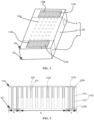
FIG. 1 andFIG. 2 are schematic diagrams of the three-dimensional structure of a heating assembly provided by an embodiment of the present disclosure; -
FIG. 3 is a schematic sectional diagram of the heating assembly provided by an embodiment of the present disclosure; -
FIG. 4 is a schematic sectional diagram of the heating assembly provided by another embodiment of the present disclosure; -
FIG. 5 is a schematic sectional diagram of a heating assembly provided by another embodiment of the present disclosure; -
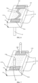
FIG. 6 and FIG. 7 are schematic diagrams of the three-dimensional structure of the heating assembly provided by another embodiment of the present disclosure; -
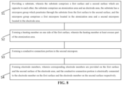
FIG. 8 is a flowchart of the preparation process of the heating assembly provided by another embodiment of the present disclosure; -
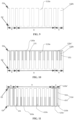
FIG. 9-FIG. 11 are schematic diagrams of the preparation process of the heating assembly provided by another embodiment of the present disclosure; -
FIG. 12 is an external schematic diagram of the electronic atomization device provided by another embodiment of the present disclosure; and -
FIG. 13 is a schematic diagram of the inside of the atomizer of the present disclosure. - As mentioned in the background, the existing heating assemblies and electronic atomization devices have poor reliability.
- A heating assembly comprises a substrate; a heating member on the atomization surface of the substrate; electrodes located on both sides of the heating member and on the same side as the atomization surface; a lead or thimble connected to the electrode.
- The above-mentioned heating assembly has poor reliability. After the investigation by the applicant, it is found that the reasons for this are as follows:
- The lead wire or thimble will pass through the atomization cavity. On the one hand, crossing the atomization cavity will reduce the space of the atomization cavity, and it is not conducive to full atomization. On the other hand, it will hinder the circulation and transmission of flue gas. Besides, the temperature of the atomization surface is high in the process of suction, and the heat is easily transferred to the lead or thimble. This will increase the temperature of the lead or thimble and even lead to instability or even failure of the electrode connection in serious cases.
- Secondly, the atomization surface has an upward structure. As power source in the electronic atomization device is below it, the external heating circuit needs to pass through the components that fix the substrate to connect with the electrode and the power source. This structure increases the processing difficulty and easily leads to the risk of liquid leakage.
- To sum up, the heating assembly has poor reliability.
- The embodiment of the present disclosure provides a heating element assembly to improve the reliability of the heating element assembly.
- The technical solutions of the present disclosure will be described clearly and completely by combining with the accompanying drawings. Obviously, the described embodiments are some embodiments of the present disclosure but not all the embodiments. Based on the embodiments of the present disclosure, all other embodiments obtained by the ordinary technical personnel in this field without requiring creative work fall within the protection scope of the present disclosure.
- In the description of the present disclosure, it should be noted that the orientation or position relationship indicated by the terms "center", "upper", "lower", "left", "right", "vertical", "horizontal", "inner" and "outer" is based on the orientation or position relationship shown in the accompanying drawings. It is only for the convenience of describing the present disclosure and simplifying the description but does not indicate or imply that the device or element must have a specific orientation, be manufactured and operated in a specific orientation. Therefore, it cannot be understood as a limitation for the present disclosure. In addition, the terms "first", "second" and "third" are only used for descriptive purposes and cannot be understood as indicating or implying relative importance.
- In the description of the present disclosure, it should be noted that unless otherwise specified and limited, the terms "install", "connect" and "connection" should be broadly understood. For example, it can be fixed connection, detachable connection or integrated connection; it can be mechanical connection or electrical connection; it can be directly connected, indirectly connected through an intermediate medium, or internally connected between two elements, wirelessly connected or wired. For ordinary technical personnel in this field, the specific meanings of the above terms in the present disclosure can be understood under specific circumstances.
- In addition, the technical features involved in different embodiments of the present disclosure described below can be combined with each other as long as they do not conflict with each other.
- This embodiment provides a
heating element assembly 10. As shown inFIG. 1 ,FIG. 2 and FIG. 3 , it comprises: - A
substrate 100, wherein the substrate comprises a first surface Q1 and a second surface Q2 which are opposite to each other, thesubstrate 100 comprises an atomization area B and electrode areas A, thesubstrate 100 has a micropore group which penetrates through thesubstrate 100 from the first surface Q1 to the second surface Q2, and the micropore group comprisesfirst micropores 110a located in the atomization area B andsecond micropores 110b located in each of the electrode areas A; - A
heating member 130 arranged on one side of the first surface Q1, wherein theheating member 130 at least crosses part of the atomization area B; - Electrode members (120a, 120b), and wherein corresponding electrode members are provided on the first surface Q1 and the second surface Q2 of the electrode area A;
- A
conductive connection portion 150, wherein theconductive connection portion 150 is located in thesecond micropore 110b, and the conductive connection portion is electrically connected to theelectrode member 120a on the first surface Q1 and theelectrode member 120b on the second surface respectively. - The
substrate 100 comprises a ceramic substrate, a glass substrate or a silicon substrate. The ceramic substrate comprises a porous ceramic substrate, and the porous ceramic substrate has large specific surface area, strong adsorption capacity and good liquid guide. It can be understood that the shape of thesubstrate 100 is not restricted as long as tobacco tar can enter thefirst micropore 110a, and thefirst micropore 110a can transfer the tobacco tar to the heating member. - In this embodiment, the electrode areas A are respectively located on both sides of the atomizing area B.
- The
first micropore 110a is used to guide liquid and transfer the tobacco tar to theheating member 130. - In this embodiment, the micropore group is an array of micropores, and the
first micropores 110a and thesecond micropores 110b are arranged in an array. There are severalfirst micropores 110a and severalsecond micropores 110b, and the pore diameter of thesecond micropore 110b is the same as that of thefirst micropore 110a. - The pore diameter of the
second micropore 110b is the same as that of thefirst micropore 110a, which makes the structure of thesubstrate 100 simple and easy to manufacture. - In other embodiments, the pore diameter of the second micropore is different from that of the first micropore.
- In an embodiment, the ratio of the thickness of the
substrate 100 to the pore diameter of thesecond micropore 110b is between 15:1 and 5: 1; the ratio of the thickness of thesubstrate 100 to the pore diameter of thefirst micropore 110a is between 15:1 and 5:1, such as 15:1, 12:1, 10:1, 8:1, or 5:1. - In a specific embodiment, the pore diameter of the
first micropore 110a is between 10 µm and 100 µm, and the pore diameter of thesecond micropore 110b is between 10 µm and 100 µm, such as 30 µm; the thickness of thesubstrate 100 is between 0.2 mm and 0.5 mm, such as 0.2 mm, 0.3 mm, 0.4 mm or 0.5 mm. - The
heating member 130 is used to atomize tobacco tar. Theheating member 130 can be a heating film, a heating circuit, a heating piece or a heating mesh. It can heat tobacco tar evenly with uniform heating temperature, and the atomized particles will not become larger due to low local temperature. This effectively makes the atomized particles uniform, improving the taste of electronic atomization device. In an embodiment, theheating member 130 is located on the first surface corresponding to the atomization area B; in other embodiments, the heating member is embedded in the first surface of the substrate. - In this embodiment, the
heating member 130 is completely arranged on the surface of the atomization area B. - In this embodiment, the heating member is a heating film, and the heating film is completely arranged on the surface of the atomization area.
- In this embodiment, the first surface Q1 of the atomization zone B is an atomization surface, and the second surface Q2 is a liquid absorption surface.
- The electrode members comprise an electrode member located on the first surface Q1 of the electrode area A and an electrode member located on the second surface Q2 of the electrode area A. In this embodiment, the electrode member is an electrode film. In other embodiments, the electrode member can also be an electrode block. The electrode member located on the first surface Q1 of the electrode area A is a first
sub-electrode member 120a. The electrode member located on the second surface Q2 of the electrode area A is a secondsub-electrode member 120b. - In this embodiment, the
second micropore 110b comprises a first sub-micropore area (not labeled) and a second sub-micropore area (not labeled) arranged in the thickness direction of thesubstrate 100, and the distance from the first sub-micropore area to the first surface Q1 is smaller than that from the second sub-micropore area to the first surface Q1. Theconductive connection portion 150 comprises a firstsub-conductive connection portion 151 covering an inner wall surface of the first sub-micropore area and a secondsub-conductive connection portion 152 covering an inner wall surface of the second sub-micropore area. The firstsub-conductive connection portion 151 contacts with the secondsub-conductive connection portion 152. The materials of the secondsub-conductive connection portion 152 and the firstsub-conductive connection portion 151 can be the same or different. - In other embodiments, the conductive connection portion is an integral structure.
- In this embodiment, the
conductive connection portion 150 is a conductive connection film, and the conductive connection film is located on an inner wall surface of thesecond micropore 110b. Both ends of the conductive connection film extend to connect to theelectrode member 120a on the first surface Q1 and theelectrode member 120b on the second surface Q2 respectively, and the thickness of the conductive connection film is less than 1/2 of the pore diameter of thesecond micropore 110b. In this case, part of thesecond micropore 110b is not fully filled. The conductive connection film can be formed integrally with the electrode film located on the first surface Q1. Secondly, less material of the conductive connection film is used, which can reduce the cost. - In a specific embodiment, the pore diameter of the
second micropore 110b is between 10 µm and 100 µm, and the thickness of the conductive connection film is between 200 nm and 10 µm. If the pore diameter of thesecond micropore 110b is too small, the filling capacity of the conductive connection film in thesecond micropore 110b will be reduced, and the conductive connection film cannot penetrate into thesecond micropore 110b. If the pore diameter of thesecond micropore 110b is too big, when the conductive connection portion is a conductive connection film, the remainingsecond micropores 110b have better liquid locking capacity. That is, even if tobacco tar enters thesecond micropore 110b, thesecond micropore 110b will lock the tobacco tar to prevent the tobacco tar from being transferred to the first surface Q1 through thesecond micropore 110b, and effectively avoid liquid leakage. - In a specific embodiment, the thickness of the electrode film is greater than that of the conductive connection film. Specifically, the thickness of the electrode film on the first surface Q1 is greater than that of the conductive connection film, and the thickness of the electrode film Q1 on the second surface is greater than that of the conductive connection film. The thickness of the electrode film is relatively large, which improves the contact performance between the electrode film on the first surface and the
heating member 130, as well as the contact performance between the electrode film on the second surface and the lead-out connection member. The thickness of the conductive connection film refers to the thickness of the conductive connection film on the side wall surface of a single side of the second micropore. - In other embodiments, the thickness of the electrode film can also be the same as that of the conductive connection film, or the thickness of the electrode film can also be smaller than that of the conductive connection film.
- In this embodiment, the materials of electrode film, conductive connection film and heating film are the same. The thickness of the electrode film on the first surface is the same as that of the heating film. The thickness of the electrode film on the first surface is the same as that on the second surface.
- In other embodiments, the thickness of the electrode film on the first surface Q1 is different from that of the electrode film on the second surface Q2.
- In a specific embodiment, the thickness of the
substrate 100 is between 0.2 mm and 1 mm, such as 0.2 mm, 0.3 mm, 0.4 mm, 0.5 mm, 0.8 mm or 1 mm, which has the following advantages: Thesubstrate 100 is thin, which can help improve the liquid guide of thefirst micropore 110a. When theconductive connection portion 150 is a conductive connection film, the area of the conductive connection film near the first surface Q1 and the area near the second surface can be easily connected together, which reduces the difficulty of preparing the conductive connection film. - The material of the
heating member 130 includes aluminum, copper, silver, gold or several alloy thereof; the material of the electrode member includes aluminum, copper, silver, gold or several alloy thereof; the material of theconductive connection portion 150 includes aluminum, copper, silver, gold or several alloy thereof. When these materials are selected, the electrical conductivity of heating member, electrode element andconductive connection portion 150 is relatively high, which is beneficial to reducing the resistance. - In an embodiment, the thickness of the heating film is between 200nm and 5µm; the resistance of the heating film is between 0.5Ω and 2Ω. At present, the voltage range of the lithium battery of electronic atomization device does not exceed 3.7V, and the power does not exceed 10W and is generally 6.5W-8.5W. Accordingly, the resistance range of the heating film needs to be set as 0.5Ω and 2Ω. Aluminum, copper, silver, gold or several alloy thereof is used as the material of heating film, and the thickness of the corresponding heating film is between 200nm and 5µm.
- This embodiment further comprises an
additional heating film 131 located on part of an inner wall surface of thefirst micropore 110a, and theadditional heating film 131 is connected to theheating member 130. - Referring to
FIG. 6 and FIG. 7 , the heating element assembly further comprises a lead-out connection member 160, and one end of the lead-out connection member 160 is connected to the electrode member of the second surface Q2. The power source in the electronic atomization device applies an electric signal to theheating member 130 through the lead-out connection member 160, the electrode member on the second surface Q2, theconductive connector 150 and the electrode member on the first surface Q1. - In this embodiment, the lead-
out connection member 160 does not need to pass through the atomization cavity, so as to prevent the lead-out connection member from hindering the circulation and transmission of flue gas. Even if theheating member 130 makes the temperature of the first surface Q1 corresponding to the atomization area A relatively high, the distance from the first surface Q1 corresponding to the atomization area A to the lead-out connection member 160 is relatively large, the heat on the first surface Q1 corresponding to the atomization area A is not easily transmitted to the lead-out connection member 160, and the temperature rise of the lead-out connection member 160 can be avoided. Therefore, the connection of the lead-out connection member 160 is relatively stable, and the lead-out connection member 160 will not become invalid. - The lead-
out connection member 160 can be a lead or thimble. - The electrode member on the second surface Q2 can be connected towards the power source without the need for the electrode member on the first surface Q1 to bypass the
substrate 100 and electrically connect to the power source, and the risk of liquid leakage can be reduced. - Once again, the heating member and the electrode element are electrically connected through the shortest path, thereby reducing the circuit loss.
- The differences between this embodiment and
Embodiment 1 are as follows: Referring toFIG. 4 , an inner surface of thefirst micropore 110a is not provided with an additional heating film, and the entire inner wall surface of thefirst micropore 110a exposes the material of thesubstrate 100. - The similarities between this embodiment and
Embodiment 1 will not be explained in detail. - The differences between this embodiment and
Embodiment 1 are as follows: Referring toFIG. 5 , theconductive connection portion 150a fully fills the second micropore. In this embodiment, the second micropore comprises a first sub-micropore area (not labeled) and a second sub-micropore area (not labeled) arranged in the thickness direction of thesubstrate 100, and the distance from the first sub-micropore area to the first surface Q1 is smaller than that from the second sub-micropore area to the first surface Q1. Theconductive connection portion 150a comprises a firstsub-conductive connection portion 151a covering an inner wall surface of the first sub-micropore area and a secondsub-conductive connection portion 152a covering an inner wall surface of the second sub-micropore area. The firstsub-conductive connection portion 151a contacts with the secondsub-conductive connection portion 152a. The materials of the secondsub-conductive connection portion 152a and the firstsub-conductive connection portion 151a can be the same or different. - The similarities between this embodiment and
Embodiment 2 will not be explained in detail. - This embodiment provides a preparation method of a heating element assembly. As shown in
FIG. 8 , it comprises: - S1: providing a substrate, wherein the substrate comprises a first surface and a second surface which are opposite to each other, and the substrate comprises an atomization area and electrode areas, the substrate has a micropore group which penetrates through the substrate from the first surface to the second surface, and the micropore group comprises first micropores located in the atomization area and second micropores located in each of the electrode areas;
- S2: forming a heating member on one side of the first surface;
- S3: forming a conductive connection portion in the second micropore;
- S4: forming electrode members, wherein corresponding electrode members are provided on the first surface and the second surface of the electrode area, and the conductive connection portion is electrically connected to the electrode member on the first surface and the electrode member on the second surface respectively.
- The steps for forming a heating film on one side of the first surface include: forming a heating film on the first surface;
The steps for forming the electrode member comprises: forming a first sub-electrode film on the first surface corresponding to the electrode area, and forming a second sub-electrode film on the second surface corresponding to the electrode area. The second micropore comprises a first sub-micropore area and a second sub-micropore area arranged in the thickness direction of the substrate, and the distance from the first sub-micropore area to the first surface is smaller than that from the second sub-micropore area to the first surface. The steps for forming a conductive connection portion in the second micropore include: forming a first sub-conductive connection portion covering an inner wall surface of the first sub-micropore area, and forming a second sub-conductive connection portion covering an inner wall surface of the second sub-micropore area; forming the first sub-electrode film and the first sub-conductive connection portion in the process of forming the heating film; forming the second sub-conductive connection portion in the process of forming the second sub-electrode film. - Referring to
FIG. 9 , a substrate is provided, comprising a first surface Q1 and a second surface Q2 which are opposite to each other, and the substrate comprises an atomization area B and electrode areas A located on the side of the atomization area; a micropore group is formed in the substrate and penetrates through the substrate from the first surface Q1 to the second surface Q2, and the micropore group comprisesfirst micropores 110a located in the atomization area B andsecond micropores 110b located in each of the electrode areas A. - The process of forming the
first micropore 110a and thesecond micropore 110b comprises a laser drilling process. - Referring to
FIG. 10 , in the process of forming theheating film 130a, a firstsub-electrode film 120a' and a firstsub-conductive connection portion 151 are formed. - This embodiment further comprises: an
additional heating film 131 is formed on part of an inner wall surface of thefirst micropore 110a in the process of forming theheating film 130a, and theadditional heating film 131 is connected to theheating film 130a. - Referring to
FIG. 11 , a secondsub-conductive connection portion 152 is formed in the process of forming the secondsub-electrode film 120b'. - The first
sub-conductive connection portion 151 and the secondsub-conductive connection portion 152 constitute aconductive connection portion 150. - The processes of forming the
heating film 130a, thefirst sub-electrode film 120a' and the firstsub-conductive connection portion 151 include physical vapor deposition, chemical vapor deposition, spraying or printing. The processes of forming the secondsub-electrode film 120b' and the secondsub-conductive connection portion 152 include physical vapor deposition, chemical vapor deposition, spraying or printing. - In this embodiment, after the first sub-electrode film, the first sub-conductive connection portion and the heating film are formed, the second sub-electrode film and the second sub-conductive connection portion are formed. In other embodiments, after the second sub-electrode film and the second sub-conductive connection portion are formed, the first sub-electrode film, the first sub-conductive connection portion and the heating film are formed.
- The differences between this embodiment and
Embodiment 4 are as follows: While the heating film, the first sub-electrode film and the first sub-conductive connection portion are formed, the second sub-electrode film and the second sub-conductive connection portion are formed. - Specifically, sputtering sources are arranged on both sides of the substrate. Sputtering source includes a first sputtering source and a second sputtering source, and the substrate is placed vertically. The first sputtering source is arranged opposite to the first surface, and the second sputtering source is arranged opposite to the second surface. The first sputtering source and the second sputtering source are sputtered simultaneously, thereby improving the process efficiency. The first sputter source is sputtered to form a heating film, a first sub-conductive connection portion and a first sub-electrode film. The second sputtering source is sputtered to form a second sub-electrode film and a second sub-conductive connection portion.
- For the heating element assemblies in
FIG. 4 and FIG. 5 , before the heating member, the conductive connection portion and the electrode members are formed, the sacrificial material is filled in the first micropore. After the heating member, the conductive connection portion and the electrode members are formed, the sacrificial material is removed. Thus, no additional heating film is formed in the first micropore. - This embodiment provides an electronic atomization device. Referring to
FIG. 12 and FIG. 13 , it comprises an atomizer 1 (FIG. 12 ) and abattery device 2. Thebattery device 2 is electrically connected to theatomizer 1 and supplies power to theatomizer 1. Theatomizer 1 is located above thebattery device 2. - The
atomizer 1 comprises the heating element assembly provided in the above embodiment. The substrate 200 (FIG. 13 ) refers to thesubstrate 100 of the above embodiment. Theatomizer 1 is provided with a lead-out connection member 160 (FIG. 13 ), and the lead-out connection member 160 is a thimble electrode. The lead-out connection member 160 is electrically connected to thebattery device 2. - The atomizer is provided with an
air outlet channel 202 and aliquid storage cavity 201 for storing tobacco tar. Theliquid storage cavity 201 is located on the side of thesubstrate 100 far away from thebattery device 2. Theliquid storage cavity 201 is in communication with the second surface of thesubstrate 200 in a liquid guiding manner, and the liquid in theliquid storage cavity 201 flows to the liquid inlet cavity through theliquid inlet 203. The first surface faces theair outlet channel 202, and the second surface faces thebattery device 2. Theliquid storage cavity 201 is spaced from theair outlet channel 202. The side of thesubstrate 200 facing away from thebattery device 2 has anatomization cavity 204, and theatomization cavity 204 is in communication with theair outlet channel 202. The lead-out connection member 160 and theair inlet channel 161 are located below thesubstrate 100. - This embodiment further provides an atomizer. Referring to
FIG. 13 , it comprises the above heating element assembly; a liquid storage cavity, wherein theliquid storage cavity 201 is in communication with the second surface of thesubstrate 200 in a liquid guiding manner. - The
atomizer 1 is provided with a lead-out connection member 160 (FIG. 13 ), and the lead-out connection member is a thimble electrode. The atomizer is provided with anair outlet channel 202 and aliquid storage cavity 201 for storing tobacco tar. Theliquid storage cavity 201 is in communication with the second surface of thesubstrate 200 in a liquid guiding manner, and the liquid in theliquid storage cavity 201 flows to the liquid inlet cavity through theliquid inlet 203. The first surface faces theair outlet channel 202. Theliquid storage cavity 201 is spaced from theair outlet channel 202. Theatomization cavity 204 faces the first surface. Theatomization cavity 204 is in communication with theair outlet channel 202. The lead-out connection member 160 and theair inlet channel 161 are located below thesubstrate 100. - Obviously, the above-mentioned embodiments only serve as the examples for clear explanation and do not limit the embodiments. For ordinary technical personnel in this field, other changes or variations in different forms can be made on the basis of the above description. It is unnecessary and impossible to list all the embodiments here. The obvious changes or variations caused thereby still fall within the protection scope of the present invention.
Claims (22)
- A heating element assembly, characterized by comprising:a substrate, wherein the substrate comprises a first surface and a second surface which are opposite to each other, the substrate comprises an atomization area and an electrode area, the substrate has a micropore group which penetrates through the substrate from the first surface to the second surface, and the micropore group comprises a first micropore located in the atomization area and a second micropore located in the electrode area;a heating member arranged on one side of the first surface, wherein the heating member at least crosses part of the atomization area;electrode members correspondingly provided on the first surface and the second surface of the electrode area; anda conductive connection portion, wherein the conductive connection portion is located in the second micropore, and the conductive connection portion is electrically connected to the electrode member on the first surface and the electrode member on the second surface respectively.
- The heating element assembly according to claim 1, characterized in that the conductive connection portion comprises a conductive connection film, and the conductive connection film is located on an inner wall surface of the second micropore.
- The heating element assembly according to claim 2, characterized in that both ends of the conductive connection film extend to be connected to the electrode member on the first surface and the electrode member on the second surface respectively, and the thickness of the conductive connection film is less than 1/2 of the pore diameter of the second micropore.
- The heating element assembly according to claim 3, characterized in that the pore diameter of the second micropore is between 10 µm and 100 µm, and the thickness of the conductive connection film is between 200 nm and 10 µm.
- The heating element assembly according to claim 1, characterized in that the heating member is completely arranged on the surface of the atomization area.
- The heating element assembly according to claim 1, characterized in that the conductive connection portion fully fills the second micropore.
- The heating element assembly according to any of claims 2-4, characterized in that the heating member comprises a heating film; the electrode member is an electrode film.
- The heating element assembly according to claim 7, characterized in that the thickness of the electrode film is greater than that of the conductive connection film.
- The heating element assembly according to claim 7, characterized in that the electrode film,the conductive connection film and the heating film are made of the same material.
- The heating element assembly according to claim 1, characterized in that the ratio of the thickness of the substrate to the pore diameter of the second micropore is between 15:1 and 5: 1; the ratio of the thickness of the substrate to the pore diameter of the first micropore is between 15:1 and 5:1.
- The heating element assembly according to claim 1 or claim 10, characterized in that the thickness of the substrate is between 0.2 mm and 1 mm.
- The heating element assembly according to claim 1, characterized in that the substrate comprises a ceramic substrate, a glass substrate or a silicon substrate.
- The heating element assembly according to claim 1, claim 2 or claim 6, characterized in that the material of the heating element includes aluminum, copper, silver, gold or several alloy thereof; the material of the electrode member includes aluminum, copper, silver, gold or several alloy thereof; the material of the conductive connection portion includes aluminum, copper, silver, gold or several alloy thereof.
- The heating element assembly according to claim 7, characterized in that the thickness of the heating film is between 200nm and 5µm; the resistance of the heating film is between 0.5Ω and 2Ω.
- The heating element assembly according to claim 1, characterized in that it further comprises a lead-out connection member, and one end of the lead-out connection member is connected to the electrode member on the second surface.
- The heating element assembly according to claim 1, characterized in that the electrode area is respectively located on both sides of the atomization area.
- A preparation method of a heating element assembly, characterized by comprising:providing a substrate, wherein the substrate comprises a first surface and a second surface which are opposite to each other, the substrate comprises an atomization area and an electrode area, the substrate has a micropore group which penetrates through the substrate from the first surface to the second surface, and the micropore group comprises a first micropore located in the atomization area and a second micropore located in the electrode area;forming a heating member on one side of the first surface, wherein the heating member at least crosses part of the atomization area;forming a conductive connection portion in the second micropore; andforming electrode members, wherein corresponding electrode members are provided on the first surface and the second surface of the electrode area, and the conductive connection portion is electrically connected to the electrode member on the first surface and the electrode member on the second surface respectively.
- The preparation method of a heating element assembly according to claim 12, characterized in that the steps for forming a heating member on one side of the first surface include: forming a heating film on the first surface;
the steps for forming the electrode member include: forming a first sub-electrode film on the first surface corresponding to the electrode area, and forming a second sub-electrode film on the second surface corresponding to the electrode area. - The preparation method of the heating element assembly according to claim 18. the second micropore comprises a first sub-micropore area and a second sub-micropore area arranged in the thickness direction of the substrate, and the distance from the first sub-micropore area to the first surface is smaller than that from the second sub-micropore area to the first surface;the steps for forming a conductive connection portion in the second micropore include: forming a first sub-conductive connection portion covering an inner wall surface of the first sub-micropore area, and forming a second sub-conductive connection portion covering an inner wall surface of the second sub-micropore area;forming the first sub-electrode film and the first sub-conductive connection portion in the process of forming the heating film; forming the second sub-conductive connection portion in the process of forming the second sub-electrode film.
- The preparation method of the heating element assembly according to claim 19, characterized in that the processes of forming the heating film, the first sub-electrode film and the first sub-conductive connection portion include physical vapor deposition, chemical vapor deposition, spraying or printing;
the processes of forming the second sub-electrode film and the second sub-conductive connection portion include physical vapor deposition, chemical vapor deposition, spraying or printing. - An atomizer, characterized by comprising the heating element assembly according to any of claims 1-16;
a liquid storage cavity, wherein the liquid storage cavity is in communication with the second surface of the substrate in a liquid guiding manner. - An electronic atomization device, characterized by comprising the atomizer according to claim 21.
Applications Claiming Priority (1)
| Application Number | Priority Date | Filing Date | Title |
|---|---|---|---|
| PCT/CN2021/138516 WO2022179262A2 (en) | 2021-12-15 | 2021-12-15 | Heating body assembly and preparation method therefor, atomizer and electronic atomization device |
Publications (2)
| Publication Number | Publication Date |
|---|---|
| EP4449917A2 true EP4449917A2 (en) | 2024-10-23 |
| EP4449917A4 EP4449917A4 (en) | 2025-01-22 |
Family
ID=83050158
Family Applications (1)
| Application Number | Title | Priority Date | Filing Date |
|---|---|---|---|
| EP21927686.2A Pending EP4449917A4 (en) | 2021-12-15 | 2021-12-15 | RADIATOR ARRANGEMENT AND MANUFACTURING METHOD THEREFOR, ATOMIZER AND ELECTRONIC ATOMIZATION DEVICE |
Country Status (3)
| Country | Link |
|---|---|
| EP (1) | EP4449917A4 (en) |
| CN (1) | CN217906333U (en) |
| WO (1) | WO2022179262A2 (en) |
Families Citing this family (3)
| Publication number | Priority date | Publication date | Assignee | Title |
|---|---|---|---|---|
| CN116420937A (en) * | 2023-03-23 | 2023-07-14 | 深圳市赛尔美电子科技有限公司 | Directional heating atomizing core and electronic atomization device |
| CN220494277U (en) * | 2023-05-12 | 2024-02-20 | 深圳市吉迩科技有限公司 | A heating component, atomizer and aerosol generating device |
| CN119033164A (en) * | 2023-05-29 | 2024-11-29 | 思摩尔国际控股有限公司 | Electronic atomizing equipment and control method and device thereof |
Family Cites Families (19)
| Publication number | Priority date | Publication date | Assignee | Title |
|---|---|---|---|---|
| WO2015058367A1 (en) * | 2013-10-23 | 2015-04-30 | 吉瑞高新科技股份有限公司 | Electronic cigarette charging device and manufacturing method for electronic cigarette charging device |
| WO2017121296A1 (en) * | 2016-01-11 | 2017-07-20 | 常州聚为智能科技有限公司 | Atomization head, atomizer and electronic cigarette comprising same |
| CN110313642B (en) * | 2018-03-30 | 2024-07-23 | 上海新型烟草制品研究院有限公司 | Atomizer core structure and electronic cigarette |
| JP3218384U (en) * | 2018-07-30 | 2018-10-11 | 東莞市国研電熱材料有限公司Key Material Co., Ltd. | Multi-temperature range heating type ceramic heating element for electronic cigarette |
| CN209376697U (en) * | 2018-11-29 | 2019-09-13 | 深圳顺络电子股份有限公司 | A kind of electronic cigarette and its chip heater |
| CN109770438B (en) * | 2019-03-25 | 2023-07-25 | 云南中烟工业有限责任公司 | Film-coated silicon-based electronic cigarette atomization chip and preparation method thereof |
| CN210329357U (en) * | 2019-06-29 | 2020-04-17 | 何锐 | Electronic cigarette atomizer |
| WO2021007776A1 (en) * | 2019-07-16 | 2021-01-21 | 深圳达钿科技有限公司 | Heating piece for atomizer, atomizer, and electronic cigarette |
| CN110447962B (en) * | 2019-07-25 | 2025-08-12 | 深圳麦克韦尔科技有限公司 | Atomizing element and electronic cigarette |
| CN110464052B (en) * | 2019-08-06 | 2025-01-10 | 深圳麦克韦尔科技有限公司 | Atomizer assembly, atomizer and electronic atomizer device |
| CN110584212B (en) * | 2019-09-16 | 2024-10-15 | 深圳麦克韦尔科技有限公司 | Atomizing core, atomizer and electronic atomizing device |
| CN211794318U (en) * | 2019-11-20 | 2020-10-30 | 广东国研新材料有限公司 | Microporous ceramic electronic cigarette oil type heating body and electronic cigarette thereof |
| CN110710731A (en) * | 2019-12-09 | 2020-01-21 | 金刚智能科技(东莞)有限公司 | Electronic cigarette atomization heating device, preparation method thereof and electronic cigarette |
| DE102019135177B4 (en) * | 2019-12-19 | 2021-07-29 | Hauni Maschinenbau Gmbh | Vaporizer unit, vaporizer assembly and vaporizer cartridge as part of an inhaler, inhaler with such a vaporizer cartridge and method for producing vaporizer units |
| CN212520793U (en) * | 2020-01-17 | 2021-02-12 | 深圳麦克韦尔科技有限公司 | Electronic atomization device and atomization assembly thereof |
| CN111466614A (en) * | 2020-04-02 | 2020-07-31 | 深圳麦克韦尔科技有限公司 | Atomizing core, atomizer and electronic atomization device |
| CN111920104A (en) * | 2020-07-28 | 2020-11-13 | 深圳麦克韦尔科技有限公司 | Atomizing core, atomizer and electronic atomization device |
| CN112089105B (en) * | 2020-08-13 | 2024-02-02 | 深圳麦克韦尔科技有限公司 | Atomizing core and atomizing device |
| CN113647696B (en) * | 2021-09-02 | 2024-07-05 | 美满芯盛(杭州)微电子有限公司 | MEMS silicon-based membrane hole atomization core and manufacturing method thereof |
-
2021
- 2021-12-15 EP EP21927686.2A patent/EP4449917A4/en active Pending
- 2021-12-15 CN CN202190000253.2U patent/CN217906333U/en active Active
- 2021-12-15 WO PCT/CN2021/138516 patent/WO2022179262A2/en not_active Ceased
Also Published As
| Publication number | Publication date |
|---|---|
| CN217906333U (en) | 2022-11-29 |
| WO2022179262A2 (en) | 2022-09-01 |
| WO2022179262A3 (en) | 2022-10-20 |
| EP4449917A4 (en) | 2025-01-22 |
Similar Documents
| Publication | Publication Date | Title |
|---|---|---|
| CN111109665A (en) | Electronic atomization device and atomizer and heating body thereof | |
| US20230337742A1 (en) | Atomizing core, atomizer, aerosol generating device and method for manufacturing atomizing core | |
| CN217906333U (en) | Heating element assembly, atomizer and electronic atomization device | |
| CN114794551A (en) | Atomization components and electronic atomization devices | |
| US20260068940A1 (en) | Heating assembly, atomizer, and electronic atomization device | |
| CN216931904U (en) | Atomizing core, atomizer and electronic atomization device | |
| CN116698924A (en) | GaN-based semiconductor gas sensor based on micro-electromechanical system | |
| CN120570422A (en) | Atomizer core and preparation method thereof, atomizer and electronic atomization device | |
| KR102818816B1 (en) | Heating assembly and electronic atomizer | |
| CN216135191U (en) | Atomizing core, atomization component and atomizer | |
| WO2022170756A1 (en) | Heating body, atomization assembly, and electronic atomization device | |
| US20240373936A1 (en) | Atomization device with good atomization effect | |
| CN219803356U (en) | Atomization device and its atomization components | |
| WO2023202219A1 (en) | Chip encapsulation structure, atomizer, and electronic atomization apparatus | |
| JP7653188B2 (en) | Atomizing core with airflow chamber | |
| CN217544609U (en) | Chip packaging structure, atomizer and electronic atomization device | |
| CN217364672U (en) | Parallel strip-shaped concave grain atomizing core | |
| CN217664227U (en) | Ultrasonic atomization assembly and ultrasonic atomization device | |
| CN116268581A (en) | Atomization module, atomization device and atomization method | |
| CN116210971A (en) | Atomization components and electronic atomization devices | |
| JPH0821255B2 (en) | Method for producing thin film solid electrolyte | |
| US20230371132A1 (en) | Heating body, vaporization assembly, and electronic vaporization device | |
| CN215270578U (en) | Electrode for atomizer, electrode for battery rod and electrode connecting assembly thereof | |
| EP4684664A1 (en) | Atomization module and atomization apparatus thereof | |
| RU2816172C1 (en) | Spraying device with good spraying effect |
Legal Events
| Date | Code | Title | Description |
|---|---|---|---|
| STAA | Information on the status of an ep patent application or granted ep patent |
Free format text: STATUS: THE INTERNATIONAL PUBLICATION HAS BEEN MADE |
|
| PUAI | Public reference made under article 153(3) epc to a published international application that has entered the european phase |
Free format text: ORIGINAL CODE: 0009012 |
|
| STAA | Information on the status of an ep patent application or granted ep patent |
Free format text: STATUS: REQUEST FOR EXAMINATION WAS MADE |
|
| 17P | Request for examination filed |
Effective date: 20240712 |
|
| AK | Designated contracting states |
Kind code of ref document: A2 Designated state(s): AL AT BE BG CH CY CZ DE DK EE ES FI FR GB GR HR HU IE IS IT LI LT LU LV MC MK MT NL NO PL PT RO RS SE SI SK SM TR |
|
| RAP3 | Party data changed (applicant data changed or rights of an application transferred) |
Owner name: SHENZHEN SMOORE TECHNOLOGY LIMITED |
|
| REG | Reference to a national code |
Ref country code: DE Ref legal event code: R079 Free format text: PREVIOUS MAIN CLASS: A24F0040460000 Ipc: H05B0003260000 |
|
| A4 | Supplementary search report drawn up and despatched |
Effective date: 20241219 |
|
| RIC1 | Information provided on ipc code assigned before grant |
Ipc: A24F 40/70 20200101ALI20241213BHEP Ipc: A24F 40/46 20200101ALI20241213BHEP Ipc: H05B 3/04 20060101ALI20241213BHEP Ipc: H05B 3/26 20060101AFI20241213BHEP |
|
| DAV | Request for validation of the european patent (deleted) | ||
| DAX | Request for extension of the european patent (deleted) | ||
| RAP3 | Party data changed (applicant data changed or rights of an application transferred) |
Owner name: SHENZHEN SMOORE TECHNOLOGY LIMITED |