EP4447124A2 - Integrated structure with trap rich regions and low resistivity regions - Google Patents
Integrated structure with trap rich regions and low resistivity regions Download PDFInfo
- Publication number
- EP4447124A2 EP4447124A2 EP24197793.3A EP24197793A EP4447124A2 EP 4447124 A2 EP4447124 A2 EP 4447124A2 EP 24197793 A EP24197793 A EP 24197793A EP 4447124 A2 EP4447124 A2 EP 4447124A2
- Authority
- EP
- European Patent Office
- Prior art keywords
- region
- semiconductor
- low resistivity
- handle substrate
- regions
- Prior art date
- Legal status (The legal status is an assumption and is not a legal conclusion. Google has not performed a legal analysis and makes no representation as to the accuracy of the status listed.)
- Pending
Links
Images

Classifications
-
- H—ELECTRICITY
- H10—SEMICONDUCTOR DEVICES; ELECTRIC SOLID-STATE DEVICES NOT OTHERWISE PROVIDED FOR
- H10D—INORGANIC ELECTRIC SEMICONDUCTOR DEVICES
- H10D86/00—Integrated devices formed in or on insulating or conducting substrates, e.g. formed in silicon-on-insulator [SOI] substrates or on stainless steel or glass substrates
- H10D86/201—Integrated devices formed in or on insulating or conducting substrates, e.g. formed in silicon-on-insulator [SOI] substrates or on stainless steel or glass substrates the substrates comprising an insulating layer on a semiconductor body, e.g. SOI
-
- H—ELECTRICITY
- H10—SEMICONDUCTOR DEVICES; ELECTRIC SOLID-STATE DEVICES NOT OTHERWISE PROVIDED FOR
- H10D—INORGANIC ELECTRIC SEMICONDUCTOR DEVICES
- H10D84/00—Integrated devices formed in or on semiconductor substrates that comprise only semiconducting layers, e.g. on Si wafers or on GaAs-on-Si wafers
- H10D84/01—Manufacture or treatment
- H10D84/0107—Integrating at least one component covered by H10D12/00 or H10D30/00 with at least one component covered by H10D8/00, H10D10/00 or H10D18/00, e.g. integrating IGFETs with BJTs
- H10D84/0109—Integrating at least one component covered by H10D12/00 or H10D30/00 with at least one component covered by H10D8/00, H10D10/00 or H10D18/00, e.g. integrating IGFETs with BJTs the at least one component covered by H10D12/00 or H10D30/00 being a MOS device
-
- H—ELECTRICITY
- H10—SEMICONDUCTOR DEVICES; ELECTRIC SOLID-STATE DEVICES NOT OTHERWISE PROVIDED FOR
- H10W—GENERIC PACKAGES, INTERCONNECTIONS, CONNECTORS OR OTHER CONSTRUCTIONAL DETAILS OF DEVICES COVERED BY CLASS H10
- H10W10/00—Isolation regions in semiconductor bodies between components of integrated devices
- H10W10/01—Manufacture or treatment
- H10W10/031—Manufacture or treatment of isolation regions comprising PN junctions
-
- H—ELECTRICITY
- H10—SEMICONDUCTOR DEVICES; ELECTRIC SOLID-STATE DEVICES NOT OTHERWISE PROVIDED FOR
- H10D—INORGANIC ELECTRIC SEMICONDUCTOR DEVICES
- H10D10/00—Bipolar junction transistors [BJT]
- H10D10/80—Heterojunction BJTs
- H10D10/821—Vertical heterojunction BJTs
- H10D10/891—Vertical heterojunction BJTs comprising lattice-mismatched active layers, e.g. SiGe strained-layer transistors
-
- H—ELECTRICITY
- H10—SEMICONDUCTOR DEVICES; ELECTRIC SOLID-STATE DEVICES NOT OTHERWISE PROVIDED FOR
- H10D—INORGANIC ELECTRIC SEMICONDUCTOR DEVICES
- H10D30/00—Field-effect transistors [FET]
- H10D30/60—Insulated-gate field-effect transistors [IGFET]
- H10D30/67—Thin-film transistors [TFT]
- H10D30/6704—Thin-film transistors [TFT] having supplementary regions or layers in the thin films or in the insulated bulk substrates for controlling properties of the device
-
- H—ELECTRICITY
- H10—SEMICONDUCTOR DEVICES; ELECTRIC SOLID-STATE DEVICES NOT OTHERWISE PROVIDED FOR
- H10D—INORGANIC ELECTRIC SEMICONDUCTOR DEVICES
- H10D62/00—Semiconductor bodies, or regions thereof, of devices having potential barriers
- H10D62/10—Shapes, relative sizes or dispositions of the regions of the semiconductor bodies; Shapes of the semiconductor bodies
- H10D62/13—Semiconductor regions connected to electrodes carrying current to be rectified, amplified or switched, e.g. source or drain regions
- H10D62/137—Collector regions of BJTs
-
- H—ELECTRICITY
- H10—SEMICONDUCTOR DEVICES; ELECTRIC SOLID-STATE DEVICES NOT OTHERWISE PROVIDED FOR
- H10D—INORGANIC ELECTRIC SEMICONDUCTOR DEVICES
- H10D62/00—Semiconductor bodies, or regions thereof, of devices having potential barriers
- H10D62/10—Shapes, relative sizes or dispositions of the regions of the semiconductor bodies; Shapes of the semiconductor bodies
- H10D62/17—Semiconductor regions connected to electrodes not carrying current to be rectified, amplified or switched, e.g. channel regions
- H10D62/351—Substrate regions of field-effect devices
- H10D62/357—Substrate regions of field-effect devices of FETs
- H10D62/364—Substrate regions of field-effect devices of FETs of IGFETs
- H10D62/371—Inactive supplementary semiconductor regions, e.g. for preventing punch-through, improving capacity effect or leakage current
-
- H—ELECTRICITY
- H10—SEMICONDUCTOR DEVICES; ELECTRIC SOLID-STATE DEVICES NOT OTHERWISE PROVIDED FOR
- H10D—INORGANIC ELECTRIC SEMICONDUCTOR DEVICES
- H10D84/00—Integrated devices formed in or on semiconductor substrates that comprise only semiconducting layers, e.g. on Si wafers or on GaAs-on-Si wafers
- H10D84/01—Manufacture or treatment
- H10D84/02—Manufacture or treatment characterised by using material-based technologies
- H10D84/03—Manufacture or treatment characterised by using material-based technologies using Group IV technology, e.g. silicon technology or silicon-carbide [SiC] technology
- H10D84/038—Manufacture or treatment characterised by using material-based technologies using Group IV technology, e.g. silicon technology or silicon-carbide [SiC] technology using silicon technology, e.g. SiGe
-
- H—ELECTRICITY
- H10—SEMICONDUCTOR DEVICES; ELECTRIC SOLID-STATE DEVICES NOT OTHERWISE PROVIDED FOR
- H10D—INORGANIC ELECTRIC SEMICONDUCTOR DEVICES
- H10D84/00—Integrated devices formed in or on semiconductor substrates that comprise only semiconducting layers, e.g. on Si wafers or on GaAs-on-Si wafers
- H10D84/40—Integrated devices formed in or on semiconductor substrates that comprise only semiconducting layers, e.g. on Si wafers or on GaAs-on-Si wafers characterised by the integration of at least one component covered by groups H10D12/00 or H10D30/00 with at least one component covered by groups H10D10/00 or H10D18/00, e.g. integration of IGFETs with BJTs
- H10D84/401—Combinations of FETs or IGBTs with BJTs
- H10D84/403—Combinations of FETs or IGBTs with BJTs and with one or more of diodes, resistors or capacitors
-
- H—ELECTRICITY
- H10—SEMICONDUCTOR DEVICES; ELECTRIC SOLID-STATE DEVICES NOT OTHERWISE PROVIDED FOR
- H10D—INORGANIC ELECTRIC SEMICONDUCTOR DEVICES
- H10D86/00—Integrated devices formed in or on insulating or conducting substrates, e.g. formed in silicon-on-insulator [SOI] substrates or on stainless steel or glass substrates
- H10D86/01—Manufacture or treatment
-
- H—ELECTRICITY
- H10—SEMICONDUCTOR DEVICES; ELECTRIC SOLID-STATE DEVICES NOT OTHERWISE PROVIDED FOR
- H10D—INORGANIC ELECTRIC SEMICONDUCTOR DEVICES
- H10D87/00—Integrated devices comprising both bulk components and either SOI or SOS components on the same substrate
-
- H—ELECTRICITY
- H10—SEMICONDUCTOR DEVICES; ELECTRIC SOLID-STATE DEVICES NOT OTHERWISE PROVIDED FOR
- H10P—GENERIC PROCESSES OR APPARATUS FOR THE MANUFACTURE OR TREATMENT OF DEVICES COVERED BY CLASS H10
- H10P90/00—Preparation of wafers not covered by a single main group of this subclass, e.g. wafer reinforcement
- H10P90/19—Preparing inhomogeneous wafers
- H10P90/1904—Preparing vertically inhomogeneous wafers
- H10P90/1906—Preparing SOI wafers
-
- H—ELECTRICITY
- H10—SEMICONDUCTOR DEVICES; ELECTRIC SOLID-STATE DEVICES NOT OTHERWISE PROVIDED FOR
- H10P—GENERIC PROCESSES OR APPARATUS FOR THE MANUFACTURE OR TREATMENT OF DEVICES COVERED BY CLASS H10
- H10P90/00—Preparation of wafers not covered by a single main group of this subclass, e.g. wafer reinforcement
- H10P90/19—Preparing inhomogeneous wafers
- H10P90/1904—Preparing vertically inhomogeneous wafers
- H10P90/1906—Preparing SOI wafers
- H10P90/1908—Preparing SOI wafers using silicon implanted buried insulating layers, e.g. oxide layers [SIMOX]
-
- H—ELECTRICITY
- H10—SEMICONDUCTOR DEVICES; ELECTRIC SOLID-STATE DEVICES NOT OTHERWISE PROVIDED FOR
- H10P—GENERIC PROCESSES OR APPARATUS FOR THE MANUFACTURE OR TREATMENT OF DEVICES COVERED BY CLASS H10
- H10P90/00—Preparation of wafers not covered by a single main group of this subclass, e.g. wafer reinforcement
- H10P90/19—Preparing inhomogeneous wafers
- H10P90/1904—Preparing vertically inhomogeneous wafers
- H10P90/1906—Preparing SOI wafers
- H10P90/1914—Preparing SOI wafers using bonding
- H10P90/1918—Preparing SOI wafers using bonding including charge trapping layers, e.g. polycrystalline materials
- H10P90/192—Preparing SOI wafers using bonding including charge trapping layers, e.g. polycrystalline materials irregularly shaped charge trapping layers
-
- H—ELECTRICITY
- H10—SEMICONDUCTOR DEVICES; ELECTRIC SOLID-STATE DEVICES NOT OTHERWISE PROVIDED FOR
- H10W—GENERIC PACKAGES, INTERCONNECTIONS, CONNECTORS OR OTHER CONSTRUCTIONAL DETAILS OF DEVICES COVERED BY CLASS H10
- H10W10/00—Isolation regions in semiconductor bodies between components of integrated devices
- H10W10/01—Manufacture or treatment
- H10W10/011—Manufacture or treatment of isolation regions comprising dielectric materials
- H10W10/014—Manufacture or treatment of isolation regions comprising dielectric materials using trench refilling with dielectric materials, e.g. shallow trench isolations
-
- H—ELECTRICITY
- H10—SEMICONDUCTOR DEVICES; ELECTRIC SOLID-STATE DEVICES NOT OTHERWISE PROVIDED FOR
- H10W—GENERIC PACKAGES, INTERCONNECTIONS, CONNECTORS OR OTHER CONSTRUCTIONAL DETAILS OF DEVICES COVERED BY CLASS H10
- H10W10/00—Isolation regions in semiconductor bodies between components of integrated devices
- H10W10/01—Manufacture or treatment
- H10W10/061—Manufacture or treatment using SOI processes together with lateral isolation, e.g. combinations of SOI and shallow trench isolations
-
- H—ELECTRICITY
- H10—SEMICONDUCTOR DEVICES; ELECTRIC SOLID-STATE DEVICES NOT OTHERWISE PROVIDED FOR
- H10W—GENERIC PACKAGES, INTERCONNECTIONS, CONNECTORS OR OTHER CONSTRUCTIONAL DETAILS OF DEVICES COVERED BY CLASS H10
- H10W10/00—Isolation regions in semiconductor bodies between components of integrated devices
- H10W10/10—Isolation regions comprising dielectric materials
- H10W10/17—Isolation regions comprising dielectric materials formed using trench refilling with dielectric materials, e.g. shallow trench isolations
-
- H—ELECTRICITY
- H10—SEMICONDUCTOR DEVICES; ELECTRIC SOLID-STATE DEVICES NOT OTHERWISE PROVIDED FOR
- H10W—GENERIC PACKAGES, INTERCONNECTIONS, CONNECTORS OR OTHER CONSTRUCTIONAL DETAILS OF DEVICES COVERED BY CLASS H10
- H10W10/00—Isolation regions in semiconductor bodies between components of integrated devices
- H10W10/10—Isolation regions comprising dielectric materials
- H10W10/181—Semiconductor-on-insulator [SOI] isolation regions, e.g. buried oxide regions of SOI wafers
-
- H—ELECTRICITY
- H10—SEMICONDUCTOR DEVICES; ELECTRIC SOLID-STATE DEVICES NOT OTHERWISE PROVIDED FOR
- H10W—GENERIC PACKAGES, INTERCONNECTIONS, CONNECTORS OR OTHER CONSTRUCTIONAL DETAILS OF DEVICES COVERED BY CLASS H10
- H10W10/00—Isolation regions in semiconductor bodies between components of integrated devices
- H10W10/30—Isolation regions comprising PN junctions
-
- H—ELECTRICITY
- H10—SEMICONDUCTOR DEVICES; ELECTRIC SOLID-STATE DEVICES NOT OTHERWISE PROVIDED FOR
- H10W—GENERIC PACKAGES, INTERCONNECTIONS, CONNECTORS OR OTHER CONSTRUCTIONAL DETAILS OF DEVICES COVERED BY CLASS H10
- H10W15/00—Highly-doped buried regions of integrated devices
-
- H—ELECTRICITY
- H10—SEMICONDUCTOR DEVICES; ELECTRIC SOLID-STATE DEVICES NOT OTHERWISE PROVIDED FOR
- H10W—GENERIC PACKAGES, INTERCONNECTIONS, CONNECTORS OR OTHER CONSTRUCTIONAL DETAILS OF DEVICES COVERED BY CLASS H10
- H10W15/00—Highly-doped buried regions of integrated devices
- H10W15/01—Manufacture or treatment
-
- H—ELECTRICITY
- H10—SEMICONDUCTOR DEVICES; ELECTRIC SOLID-STATE DEVICES NOT OTHERWISE PROVIDED FOR
- H10W—GENERIC PACKAGES, INTERCONNECTIONS, CONNECTORS OR OTHER CONSTRUCTIONAL DETAILS OF DEVICES COVERED BY CLASS H10
- H10W44/00—Electrical arrangements for controlling or matching impedance
- H10W44/20—Electrical arrangements for controlling or matching impedance at high-frequency [HF] or radio frequency [RF]
-
- H—ELECTRICITY
- H10—SEMICONDUCTOR DEVICES; ELECTRIC SOLID-STATE DEVICES NOT OTHERWISE PROVIDED FOR
- H10D—INORGANIC ELECTRIC SEMICONDUCTOR DEVICES
- H10D84/00—Integrated devices formed in or on semiconductor substrates that comprise only semiconducting layers, e.g. on Si wafers or on GaAs-on-Si wafers
- H10D84/40—Integrated devices formed in or on semiconductor substrates that comprise only semiconducting layers, e.g. on Si wafers or on GaAs-on-Si wafers characterised by the integration of at least one component covered by groups H10D12/00 or H10D30/00 with at least one component covered by groups H10D10/00 or H10D18/00, e.g. integration of IGFETs with BJTs
- H10D84/401—Combinations of FETs or IGBTs with BJTs
-
- H—ELECTRICITY
- H10—SEMICONDUCTOR DEVICES; ELECTRIC SOLID-STATE DEVICES NOT OTHERWISE PROVIDED FOR
- H10D—INORGANIC ELECTRIC SEMICONDUCTOR DEVICES
- H10D89/00—Aspects of integrated devices not covered by groups H10D84/00 - H10D88/00
- H10D89/60—Integrated devices comprising arrangements for electrical or thermal protection, e.g. protection circuits against electrostatic discharge [ESD]
- H10D89/601—Integrated devices comprising arrangements for electrical or thermal protection, e.g. protection circuits against electrostatic discharge [ESD] for devices having insulated gate electrodes, e.g. for IGFETs or IGBTs
- H10D89/931—Integrated devices comprising arrangements for electrical or thermal protection, e.g. protection circuits against electrostatic discharge [ESD] for devices having insulated gate electrodes, e.g. for IGFETs or IGBTs characterised by the dispositions of the protective arrangements
-
- H—ELECTRICITY
- H10—SEMICONDUCTOR DEVICES; ELECTRIC SOLID-STATE DEVICES NOT OTHERWISE PROVIDED FOR
- H10W—GENERIC PACKAGES, INTERCONNECTIONS, CONNECTORS OR OTHER CONSTRUCTIONAL DETAILS OF DEVICES COVERED BY CLASS H10
- H10W44/00—Electrical arrangements for controlling or matching impedance
- H10W44/20—Electrical arrangements for controlling or matching impedance at high-frequency [HF] or radio frequency [RF]
- H10W44/241—Electrical arrangements for controlling or matching impedance at high-frequency [HF] or radio frequency [RF] for passive devices or passive elements
Definitions
- the present disclosure relates to semiconductor structures and, more particularly, to an integrated structure with trap rich regions (high resistivity regions) and low resistivity regions and methods of manufacture.
- BiCMOS integration on high resistivity semiconductor substrates requires different parameters for different devices. These different parameters may not be compatible amongst all of the integrated devices, e.g., circuitry, residing on the same substrate. In the manufacturing process, these different parameters may also result in low yields for other devices.
- a structure comprises: a handle substrate comprising high resistivity semiconductor material; a buried insulator layer above the handle substrate; a semiconductor layer on the buried insulator layer; an active device over the semiconductor layer; a non-single-crystal semiconductor region in the handle substrate underneath the active device and contacting an underside of the buried insulator layer; and a low resistivity region floating in the handle substrate and which is below the active device.
- a method comprises: forming an active device over a high resistivity semiconductor substrate; and forming a low resistivity region floating in the high resistivity semiconductor substrate and which is below the active device.
- the present disclosure relates to semiconductor structures and, more particularly, to a structure with a trap rich region (high resistivity region) and a low resistivity region and methods of manufacture. More specifically, the present disclosure is directed to a BiCMOS integrated structure on a high resistivity wafer with trap rich implant regions and low resistivity implant regions.
- the integration scheme maintains high NPN yield with reduced device to device leakage for BiCMOS integration, in addition to maintaining back end of the line (BEOL) passive device and RF FET performance (e.g., switches).
- BEOL back end of the line
- RF FET performance e.g., switches.
- the present disclosure also provides the benefit of radiation hardening of FET devices.
- the structure may include an integrated circuit for radiation hardened electronics.
- the structure includes a high resistivity semiconductor material comprising semiconductor-on-insulator (SOI) technology.
- SOI semiconductor-on-insulator
- the structure includes a region with a high resistivity implant touching a buried insulator material, forming a trap rich layer below RF FETs or BEOL passive devices.
- a hybrid region may be surrounded by a deep trench isolation structure and includes a low resistivity region below a bipolar device, FET, or diode, etc.
- Another region includes both a trap rich region and low resistivity region below a logic FET or other active device.
- Another region with a FET or passive device is completely devoid of both the trap rich region and low resistivity region.
- the structure of the present disclosure can be manufactured in a number of ways using a number of different tools.
- the methodologies and tools are used to form structures with dimensions in the micrometer and nanometer scale.
- the methodologies, i.e., technologies, employed to manufacture the structure of the present disclosure have been adopted from integrated circuit (IC) technology.
- the structures are built on wafers and are realized in films of material patterned by photolithographic processes on the top of a wafer.
- the fabrication of the structure uses three basic building blocks: (i) deposition of thin films of material on a substrate, (ii) applying a patterned mask on top of the films by photolithographic imaging, and (iii) etching the films selectively to the mask.
- precleaning processes may be used to clean etched surfaces of any contaminants, as is known in the art.
- rapid thermal anneal processes may be used to drive-in dopants or material layers as is known in the art.
- FIG. 1 shows a structure with both a high resistivity region and a low resistivity region under an active device, amongst other features, and respective fabrication processes in accordance with the present disclosure.
- the structure 10 includes a device region 100 comprising an active device 14 between shallow trench isolation structures 16.
- the active device 14 may be a logic device (e.g., FET) for radiation hardened applications.
- the active device 14 may be provided on a semiconductor substrate 12 as described in more detail herein.
- the active device 14 includes a gate electrode 14a surrounded by sidewall spacers 14b.
- the gate electrode 14a may be any known workfunction metal, e.g., Ti, TiN, TiAl, etc., or a polysilicon material.
- the sidewall spacers 14b may be an oxide and/or nitride material fabricated using conventional deposition methods, e.g., chemical vapor deposition (CVD), followed by a conventional anisotropic etching process as is known in the art.
- the active device 14 also includes source and drain regions 14c which are provided in the semiconductor substrate 12 (and more specifically, on a semiconductor-on-insulator substrate).
- the gate electrode 14a may be provided on a gate dielectric material, e.g., a high-k gate dielectric material, e.g., HfO 2 Al 2 O 3 , Ta 2 O 3 , TiO 2 , La 2 O 3 , SrTiO 3 , LaAlO 3 , ZrO 2 , Y 2 O 3 , Gd 2 O 3 , and combinations including multilayers thereof.
- a gate dielectric material e.g., a high-k gate dielectric material, e.g., HfO 2 Al 2 O 3 , Ta 2 O 3 , TiO 2 , La 2 O 3 , SrTiO 3 , LaAlO 3 , ZrO 2 , Y 2 O 3 , Gd 2 O 3 , and combinations including multilayers thereof.
- the device 14 can be fabricated using conventional CMOS processes. For example, in standard CMOS processing, a gate dielectric material and gate electrode material are formed, e.g., deposited, onto the semiconductor substrate 12, followed by a conventional patterning process. An insulator material such as nitride and/or oxide can be deposited on the patterned materials, followed by an anisotropic etching process to form the sidewall spacers 14b.
- the source and drain regions 14c may be formed by a conventional ion implantation process or an epitaxial growth process with an in-situ doping as is known in the art.
- source and drain regions 14c could also be formed by using both epitaxial growth and implantation processes such that the top of the source and drain regions 14c is above the top of the semiconductor substrate 12, i.e., top semiconductor layer 12c.
- a silicide contact may be formed on the source and drain regions 14c and gate electrode (e.g., polysilicon material).
- the silicide process begins with deposition of a thin transition metal layer, e.g., nickel, cobalt or titanium, over fully formed and patterned semiconductor devices (e.g., doped or ion implanted source and drain regions 14c and respective device (if polysilicon material).
- the structure is heated allowing the transition metal to react with exposed silicon (or other semiconductor material as described herein) in the active regions of the semiconductor device (e.g., source, drain, gate contact region) forming a low-resistance transition metal silicide.
- exposed silicon or other semiconductor material as described herein
- any remaining transition metal is removed by chemical etching, leaving silicide contacts in the active regions of the device. It should be understood by those of skill in the art that silicide contacts will not be required on the devices when a gate structure is composed of a metal material.
- the semiconductor substrate 12 may comprise semiconductor-on-insulator (SOI) technology.
- the semiconductor substrate 12 includes, from bottom to top, a handle substrate 12a, a buried insulator layer 12b, and a top semiconductor layer 12c.
- the handle substrate 12a may be a high resistivity substrate to provide increased radio frequency (RF) performance.
- the handle substrate 12a may be a P- semiconductor substrate with a resistivity in the range of about between 1Kohm-cm to greater than 10Kohm-cm, as an illustrative example.
- the handle substrate 12a provides mechanical support to the buried insulator layer 12b and the top semiconductor layer 12c.
- the buried insulator layer 12b may include a dielectric material such as silicon dioxide, silicon nitride, silicon oxynitride, boron nitride or a combination thereof.
- the buried insulator layer 12b may be a buried oxide (BOX).
- the buried insulator layer 12b may be formed by a deposition process, such as chemical vapor deposition (CVD), plasma enhanced chemical vapor deposition CVD (PECVD) or physical vapor deposition (PVD).
- the buried insulator layer 12b may be formed using a thermal growth process, e.g., thermal oxidation, or an implanting process where oxygen atoms are implanted and annealed into the handle substrate 12a.
- the handle substrate 12a and top semiconductor layer 12c may include any appropriate semiconductor material, e.g., Si, Ge, SiGe, SiC, SiGeC, a III-V compound semiconductor, an II-VI compound semiconductor or any combinations thereof.
- the handle substrate 12a and the top semiconductor layer 12c comprise a single crystalline semiconductor material, such as, for example, single crystalline silicon with any suitable crystallographic orientation (e.g., a (100), (110), (111), or (001) crystallographic orientation).
- an optional non-single-crystal semiconductor region 18 may be formed in the handle substrate 12a.
- the non-single-crystal semiconductor region 18 may be trap rich region and, more specifically, an amorphous region or polysilicon region.
- the non-single-crystal semiconductor region 18 may be formed directly underneath and in contact with an underside of the buried insulator layer 12b, underneath the device 14.
- the non-single-crystal semiconductor region 18 may reduce the effects of a total ionizing dose (TID).
- TID total ionizing dose
- the non-single-crystal semiconductor region 18 can create traps so that the charge carriers formed as a result of ionizing radiation can recombine so that a Vt (or performance) of the device 14 does not change.
- the effects of total ionizing dose in electronics can include a parametric degradation that leads to device degradation and functional failure. This includes threshold voltage shifts which can alter the way electronics function, such as how they are activated or deactivated. Reduced gain, increased leakage, timing changes and decreased functionality can also occur.
- the non-single-crystal semiconductor region 18 may be formed by an implantation process, using a patterned implantation mask.
- the non-single-crystal semiconductor region 18 may be formed by a blanket argon implant process; although the use of any non-dopant or noble gas is contemplated herein for the implantation process.
- the handle substrate 12a can be subjected to an argon implant at 300 KeV and a dose of 1 ⁇ 10 15 cm -2 .
- implant parameters are contemplated herein depending on the desired thickness and depth of the implant region including, e.g., the ion dose may be less than or greater than 1 ⁇ 10 15 cm -2 or within a range of 1 ⁇ 10 13 cm -2 to 5 ⁇ 10 16 cm -2 .
- the energy of the implant can be adjusted depending on the desired depth from surface of the trap rich region.
- the thickness of the non-single-crystal semiconductor region 18 can be adjusted depending on the parameters of the implantation process. In this way, the non-single-crystal semiconductor region 18 may be a high resistivity region, e.g., higher than the resistivity of the handle substrate 12a, which will reduce the TID.
- FIG. 1 further shows a low resistivity region 20 in the handle substrate 12a.
- the low resistivity region 20 may be used to reduce single event upsets.
- the single-event upset SEU
- SEU single-event upset
- the state change is a result of the free charge (electron hole pair (EHP)) created by ionization in or close to an important node of a logic element.
- EHP electron hole pair
- the error in device output or operation caused as a result of the strike is called an SEU or a soft error.
- the low resistivity region 20 may be an implanted region comprising boron, which has a lower resistivity than the handle substrate 12a.
- the lower resistivity region 20 may be less than 100 Ohm-cm to 0.001 Ohm-cm depending on the implant conditions.
- the low resistivity region 20 is a floating region (e.g., no electrical connections) that is separated from and makes no contact with the non-single-crystal semiconductor region 18 or the device 14.
- the low resistivity region 20 may be separated from the non-single-crystal semiconductor region 18 by a high resistivity region of the handle substrate 12a by a distance "X", where "X" is about 0.5 microns; although other distances are also contemplated herein depending on the desired device performance, as well as the thickness of the handle substrate 12a.
- the low resistivity region 20 may be formed by an implantation process using a patterned implantation mask.
- the low resistivity region 20 may be formed by a blanket boron implant process.
- the handle substrate 12a can be subjected to a boron implant at 400keV and a dose of 5E11 cm -2 .
- other implant parameters are contemplated herein depending on the desired thickness and depth of the implant region including, e.g., the ion dose may be less than or greater than 5E11 cm -2 or within a range of 5E10 to 1E17 cm -2 .
- the energy of the implant can be adjust depending on the desired depth of the low resistivity region 20.
- the thickness of the low resistivity region 20 can be adjusted depending on the parameters of the implantation process.
- respective patterned implantation masks may be used to define selected areas exposed for the implantations.
- the implantation masks may include a layer of a light-sensitive material, such as an organic photoresist, applied by a spin coating process, pre-baked, exposed to light projected through a photomask, baked after exposure, and developed with a chemical developer.
- a light-sensitive material such as an organic photoresist
- Each of the implantation masks has a thickness and stopping power sufficient to block masked areas against receiving a dose of the implanted ions.
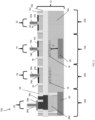
- FIG. 2 shows an integrated design layout in accordance with aspects of the present disclosure.
- the integrated design layout 10a includes four device regions: device region 100, device region 200, device region 300, and device region 400.
- each of the device regions 100, 200, 300, 400 are provided on the semiconductor substrate 12 comprising the handle substrate 12a, the buried insulator layer 12b and the top semiconductor layer 12c as described with respect to FIG. 1 .
- device region 100 is the device region 100 described with respect to FIG. 1 .
- the device region 200 may include a standard logic device 22.
- the device region 200 may include a passive device.
- the logic device 22 includes a gate electrode 22a surrounded by sidewall spacers 22b.
- the gate electrode 20a may be any known workfunction metal, e.g., Ti, TiN, TiAl, etc., or a polysilicon material.
- the sidewall spacers 22c may be an oxide and/or nitride material fabricated using conventional deposition methods, e.g., CVD, followed by a conventional anisotropic etching process as is known in the art.
- the active device 22 also includes source and drain regions 22c which are provided in the semiconductor layer 12c.
- the gate electrode 22a may be provided on a gate dielectric material, e.g., a high-k gate dielectric material, e.g., HfO 2 Al 2 O 3 , Ta 2 O 3 , TiO 2 , La 2 O 3 , SrTiO 3 , LaAlO 3 , ZrO 2 , Y 2 O 3 , Gd 2 O 3 , and combinations including multilayers thereof.
- the device region 200 is devoid of any high resistivity region and low resistivity region.
- the device region 300 includes a standard RF device or BEOL passive device 24.
- the standard RF device 24 includes a gate electrode 24a surrounded by sidewall spacers 24b, in addition to source and drain regions 24c.
- the device region 300 also includes the non-single-crystal semiconductor region 18 formed directly underneath and in contact with an underside of the buried insulator layer 12b, underneath the device 24.
- the non-single-crystal semiconductor region 18 in device regions 100 and 300 may be formed in the same implantation process with the same patterned mask.
- the low resistivity region 20 may be an implanted region comprising argon.
- the device region 300 is devoid of any low resistivity region.
- the device region 400 includes a heterojunction bipolar transistor 26, e.g., NPN.
- the device region 400 may include other devices such as a diode or passive device.
- the heterojunction bipolar transistor 26 includes an emitter 26a, an extrinsic/intrinsic base region 26b, a collector region 26c and a sub-collector region 26d.
- the collector region 26c is formed over the sub-collector region 26d.
- the collector region 26c may be Si material, as an example.
- the sub-collector region 26d may be formed in the handle substrate 12a by an ion implant process, using a patterned mask as is known in the art.
- the implant can be a n-type dopant, e.g., Arsenic (As), Phosphorus (P) and Sb, among other suitable examples.
- the extrinsic/intrinsic base region 26b may be a semiconductor material, e.g., SiGe, epitaxially grown on the top semiconductor layer 12c.
- the emitter 26a may be an N-type semiconductor material epitaxially grown on the intrinsic base region 26b.
- the collector region 26c and sub-collector region 26d are isolated within deep trench isolation structures 28.
- the deep trench isolation structures 28 can be formed by conventional lithography, etching and deposition methods known to those of skill in the art. For example, a resist formed over the top semiconductor layer 12c is exposed to energy (light) and developed utilizing a conventional resist developer to form a pattern (opening). An etching process with a selective chemistry, e.g., reactive ion etching (RIE), will be used to transfer the pattern from the patterned photoresist layer to the top semiconductor layer 12c and handle substrate 12a to form one or more trenches.
- RIE reactive ion etching
- insulator material can be deposited by any conventional deposition processes, e.g., CVD processes. Any residual material on the surface of the top semiconductor layer 12c can be removed by conventional chemical mechanical polishing (CMP) processes.
- CMP chemical mechanical polishing
- the low resistivity region 20 is formed in the handle substrate 12a under the sub-collector region 26d. In further embodiments, the low resistivity region 20 does not contact the sub-collector region 26d. The low resistivity region 20 may contact the deep trench isolation regions 28 in order to isolate the device 26.
- the low resistivity region 20 in device regions 100 and 400 may be formed in the same implantation process with the same mask. As previously disclosed, the low resistivity region 20 may be an implanted region comprising boron, which has a lower resistivity than the handle substrate 12a.
- SoC system on chip
- the SoC is an integrated circuit (also known as a "chip") that integrates all components of an electronic system on a single chip or substrate. As the components are integrated on a single substrate, SoCs consume much less power and take up much less area than multi-chip designs with equivalent functionality. Because of this, SoCs are becoming the dominant force in the mobile computing (such as in Smartphones) and edge computing markets. SoC is also used in embedded systems and the Internet of Things.
- the method(s) as described above is used in the fabrication of integrated circuit chips.
- the resulting integrated circuit chips can be distributed by the fabricator in raw wafer form (that is, as a single wafer that has multiple unpackaged chips), as a bare die, or in a packaged form.
- the chip is mounted in a single chip package (such as a plastic carrier, with leads that are affixed to a motherboard or other higher level carrier) or in a multichip package (such as a ceramic carrier that has either or both surface interconnections or buried interconnections).
- the chip is then integrated with other chips, discrete circuit elements, and/or other signal processing devices as part of either (a) an intermediate product, such as a motherboard, or (b) an end product.
- the end product can be any product that includes integrated circuit chips, ranging from toys and other low-end applications to advanced computer products having a display, a keyboard or other input device, and a central processor.
Landscapes
- Element Separation (AREA)
- Metal-Oxide And Bipolar Metal-Oxide Semiconductor Integrated Circuits (AREA)
- Semiconductor Memories (AREA)
- Non-Volatile Memory (AREA)
Abstract
Description
- This invention was made with government support under Contract #
HR0011-20-3-0002 - The present disclosure relates to semiconductor structures and, more particularly, to an integrated structure with trap rich regions (high resistivity regions) and low resistivity regions and methods of manufacture.
- BiCMOS integration on high resistivity semiconductor substrates requires different parameters for different devices. These different parameters may not be compatible amongst all of the integrated devices, e.g., circuitry, residing on the same substrate. In the manufacturing process, these different parameters may also result in low yields for other devices.
- In an aspect of the disclosure, a structure comprises: a handle substrate comprising high resistivity semiconductor material; a buried insulator layer above the handle substrate; a semiconductor layer on the buried insulator layer; an active device over the semiconductor layer; a non-single-crystal semiconductor region in the handle substrate underneath the active device and contacting an underside of the buried insulator layer; and a low resistivity region floating in the handle substrate and which is below the active device.
- Additional features of the structure are set forth in dependent claims 2 to 7.
- In an aspect of the disclosure, a method comprises: forming an active device over a high resistivity semiconductor substrate; and forming a low resistivity region floating in the high resistivity semiconductor substrate and which is below the active device.
- The present disclosure is described in the detailed description which follows, in reference to the noted plurality of drawings by way of non-limiting examples of exemplary embodiments of the present disclosure.
-
FIG. 1 shows a structure with both a high resistivity region and a low resistivity region under an active device, amongst other features, and respective fabrication processes in accordance with the present disclosure. -
FIG. 2 shows an integrated design layout and respective fabrication processes in accordance with the present disclosure. - The present disclosure relates to semiconductor structures and, more particularly, to a structure with a trap rich region (high resistivity region) and a low resistivity region and methods of manufacture. More specifically, the present disclosure is directed to a BiCMOS integrated structure on a high resistivity wafer with trap rich implant regions and low resistivity implant regions. Advantageously, the integration scheme maintains high NPN yield with reduced device to device leakage for BiCMOS integration, in addition to maintaining back end of the line (BEOL) passive device and RF FET performance (e.g., switches). The present disclosure also provides the benefit of radiation hardening of FET devices.
- In embodiments, the structure may include an integrated circuit for radiation hardened electronics. The structure includes a high resistivity semiconductor material comprising semiconductor-on-insulator (SOI) technology. The structure includes a region with a high resistivity implant touching a buried insulator material, forming a trap rich layer below RF FETs or BEOL passive devices. A hybrid region may be surrounded by a deep trench isolation structure and includes a low resistivity region below a bipolar device, FET, or diode, etc. Another region includes both a trap rich region and low resistivity region below a logic FET or other active device. Another region with a FET or passive device is completely devoid of both the trap rich region and low resistivity region.
- The structure of the present disclosure can be manufactured in a number of ways using a number of different tools. In general, though, the methodologies and tools are used to form structures with dimensions in the micrometer and nanometer scale. The methodologies, i.e., technologies, employed to manufacture the structure of the present disclosure have been adopted from integrated circuit (IC) technology. For example, the structures are built on wafers and are realized in films of material patterned by photolithographic processes on the top of a wafer. In particular, the fabrication of the structure uses three basic building blocks: (i) deposition of thin films of material on a substrate, (ii) applying a patterned mask on top of the films by photolithographic imaging, and (iii) etching the films selectively to the mask. In addition, precleaning processes may be used to clean etched surfaces of any contaminants, as is known in the art. Moreover, when necessary, rapid thermal anneal processes may be used to drive-in dopants or material layers as is known in the art.
-
FIG. 1 shows a structure with both a high resistivity region and a low resistivity region under an active device, amongst other features, and respective fabrication processes in accordance with the present disclosure. In particular, thestructure 10 includes adevice region 100 comprising anactive device 14 between shallowtrench isolation structures 16. In more specific embodiments, theactive device 14 may be a logic device (e.g., FET) for radiation hardened applications. Theactive device 14 may be provided on asemiconductor substrate 12 as described in more detail herein. - In embodiments, the
active device 14 includes agate electrode 14a surrounded bysidewall spacers 14b. Thegate electrode 14a may be any known workfunction metal, e.g., Ti, TiN, TiAl, etc., or a polysilicon material. Thesidewall spacers 14b may be an oxide and/or nitride material fabricated using conventional deposition methods, e.g., chemical vapor deposition (CVD), followed by a conventional anisotropic etching process as is known in the art. Theactive device 14 also includes source anddrain regions 14c which are provided in the semiconductor substrate 12 (and more specifically, on a semiconductor-on-insulator substrate). Thegate electrode 14a may be provided on a gate dielectric material, e.g., a high-k gate dielectric material, e.g., HfO2 Al2O3, Ta2O3, TiO2, La2O3, SrTiO3, LaAlO3, ZrO2, Y2O3, Gd2O3, and combinations including multilayers thereof. - The
device 14 can be fabricated using conventional CMOS processes. For example, in standard CMOS processing, a gate dielectric material and gate electrode material are formed, e.g., deposited, onto thesemiconductor substrate 12, followed by a conventional patterning process. An insulator material such as nitride and/or oxide can be deposited on the patterned materials, followed by an anisotropic etching process to form thesidewall spacers 14b. The source anddrain regions 14c may be formed by a conventional ion implantation process or an epitaxial growth process with an in-situ doping as is known in the art. It is well understood by those of skill in the art that the source anddrain regions 14c could also be formed by using both epitaxial growth and implantation processes such that the top of the source anddrain regions 14c is above the top of thesemiconductor substrate 12, i.e.,top semiconductor layer 12c. - Although not critical to the understanding of the present disclosure, a silicide contact may be formed on the source and
drain regions 14c and gate electrode (e.g., polysilicon material). As should be understood by those of skill in the art, the silicide process begins with deposition of a thin transition metal layer, e.g., nickel, cobalt or titanium, over fully formed and patterned semiconductor devices (e.g., doped or ion implanted source anddrain regions 14c and respective device (if polysilicon material). After deposition of the material, the structure is heated allowing the transition metal to react with exposed silicon (or other semiconductor material as described herein) in the active regions of the semiconductor device (e.g., source, drain, gate contact region) forming a low-resistance transition metal silicide. Following the reaction, any remaining transition metal is removed by chemical etching, leaving silicide contacts in the active regions of the device. It should be understood by those of skill in the art that silicide contacts will not be required on the devices when a gate structure is composed of a metal material. - Still referring to
FIG. 1 , thesemiconductor substrate 12 may comprise semiconductor-on-insulator (SOI) technology. Thesemiconductor substrate 12 includes, from bottom to top, ahandle substrate 12a, a buriedinsulator layer 12b, and atop semiconductor layer 12c. Thehandle substrate 12a may be a high resistivity substrate to provide increased radio frequency (RF) performance. In embodiments, thehandle substrate 12a may be a P- semiconductor substrate with a resistivity in the range of about between 1Kohm-cm to greater than 10Kohm-cm, as an illustrative example. Thehandle substrate 12a provides mechanical support to the buriedinsulator layer 12b and thetop semiconductor layer 12c. - The buried
insulator layer 12b may include a dielectric material such as silicon dioxide, silicon nitride, silicon oxynitride, boron nitride or a combination thereof. In one preferred embodiment, the buriedinsulator layer 12b may be a buried oxide (BOX). The buriedinsulator layer 12b may be formed by a deposition process, such as chemical vapor deposition (CVD), plasma enhanced chemical vapor deposition CVD (PECVD) or physical vapor deposition (PVD). In another embodiment, the buriedinsulator layer 12b may be formed using a thermal growth process, e.g., thermal oxidation, or an implanting process where oxygen atoms are implanted and annealed into thehandle substrate 12a. - The
handle substrate 12a andtop semiconductor layer 12c may include any appropriate semiconductor material, e.g., Si, Ge, SiGe, SiC, SiGeC, a III-V compound semiconductor, an II-VI compound semiconductor or any combinations thereof. Typically, thehandle substrate 12a and thetop semiconductor layer 12c comprise a single crystalline semiconductor material, such as, for example, single crystalline silicon with any suitable crystallographic orientation (e.g., a (100), (110), (111), or (001) crystallographic orientation). - Still referring to
FIG. 1 , an optional non-single-crystal semiconductor region 18 may be formed in thehandle substrate 12a. In more specific embodiments, the non-single-crystal semiconductor region 18 may be trap rich region and, more specifically, an amorphous region or polysilicon region. In embodiments, the non-single-crystal semiconductor region 18 may be formed directly underneath and in contact with an underside of the buriedinsulator layer 12b, underneath thedevice 14. - In embodiments, the non-single-
crystal semiconductor region 18 may reduce the effects of a total ionizing dose (TID). For example, the non-single-crystal semiconductor region 18 can create traps so that the charge carriers formed as a result of ionizing radiation can recombine so that a Vt (or performance) of thedevice 14 does not change. It should be understood by those of ordinary skill in the art that the effects of total ionizing dose in electronics can include a parametric degradation that leads to device degradation and functional failure. This includes threshold voltage shifts which can alter the way electronics function, such as how they are activated or deactivated. Reduced gain, increased leakage, timing changes and decreased functionality can also occur. - The non-single-
crystal semiconductor region 18 may be formed by an implantation process, using a patterned implantation mask. For example, the non-single-crystal semiconductor region 18 may be formed by a blanket argon implant process; although the use of any non-dopant or noble gas is contemplated herein for the implantation process. - As an illustrative, non-limiting example, the
handle substrate 12a can be subjected to an argon implant at 300 KeV and a dose of 1×1015 cm-2. By way of further illustrative examples, other implant parameters are contemplated herein depending on the desired thickness and depth of the implant region including, e.g., the ion dose may be less than or greater than 1×1015 cm-2 or within a range of 1×1013 cm-2 to 5×1016 cm-2. Similarly the energy of the implant can be adjusted depending on the desired depth from surface of the trap rich region. The thickness of the non-single-crystal semiconductor region 18 can be adjusted depending on the parameters of the implantation process. In this way, the non-single-crystal semiconductor region 18 may be a high resistivity region, e.g., higher than the resistivity of thehandle substrate 12a, which will reduce the TID. -
FIG. 1 further shows alow resistivity region 20 in thehandle substrate 12a. In embodiments, thelow resistivity region 20 may be used to reduce single event upsets. As should be understood by those of skill in the art, the single-event upset (SEU) is a change of state caused by one single ionizing particle (ions, electrons, photons, etc.) striking a sensitive node in a micro-electronic device, e.g.,device 14. The state change is a result of the free charge (electron hole pair (EHP)) created by ionization in or close to an important node of a logic element. The error in device output or operation caused as a result of the strike is called an SEU or a soft error. - The
low resistivity region 20 may be an implanted region comprising boron, which has a lower resistivity than thehandle substrate 12a. For example, thelower resistivity region 20 may be less than 100 Ohm-cm to 0.001 Ohm-cm depending on the implant conditions. In embodiments, thelow resistivity region 20 is a floating region (e.g., no electrical connections) that is separated from and makes no contact with the non-single-crystal semiconductor region 18 or thedevice 14. In embodiments, thelow resistivity region 20 may be separated from the non-single-crystal semiconductor region 18 by a high resistivity region of thehandle substrate 12a by a distance "X", where "X" is about 0.5 microns; although other distances are also contemplated herein depending on the desired device performance, as well as the thickness of thehandle substrate 12a. - The
low resistivity region 20 may be formed by an implantation process using a patterned implantation mask. For example, thelow resistivity region 20 may be formed by a blanket boron implant process. As an illustrative, non-limiting example, thehandle substrate 12a can be subjected to a boron implant at 400keV and a dose of 5E11 cm-2. By way of further illustrative examples, other implant parameters are contemplated herein depending on the desired thickness and depth of the implant region including, e.g., the ion dose may be less than or greater than 5E11 cm-2 or within a range of 5E10 to 1E17 cm-2. The energy of the implant can be adjust depending on the desired depth of thelow resistivity region 20. The thickness of thelow resistivity region 20 can be adjusted depending on the parameters of the implantation process. - For both the
low resistivity region 20 and the non-single-crystal semiconductor region 18, respective patterned implantation masks may be used to define selected areas exposed for the implantations. The implantation masks may include a layer of a light-sensitive material, such as an organic photoresist, applied by a spin coating process, pre-baked, exposed to light projected through a photomask, baked after exposure, and developed with a chemical developer. Each of the implantation masks has a thickness and stopping power sufficient to block masked areas against receiving a dose of the implanted ions. -
FIG. 2 shows an integrated design layout in accordance with aspects of the present disclosure. In particular, theintegrated design layout 10a includes four device regions:device region 100,device region 200,device region 300, anddevice region 400. As shown inFIG. 2 , each of thedevice regions semiconductor substrate 12 comprising thehandle substrate 12a, the buriedinsulator layer 12b and thetop semiconductor layer 12c as described with respect toFIG. 1 . It should also be recognized thatdevice region 100 is thedevice region 100 described with respect toFIG. 1 . - The
device region 200 may include astandard logic device 22. Alternatively, thedevice region 200 may include a passive device. In the implementation of thestandard logic device 22, thelogic device 22 includes agate electrode 22a surrounded by sidewall spacers 22b. The gate electrode 20a may be any known workfunction metal, e.g., Ti, TiN, TiAl, etc., or a polysilicon material. Thesidewall spacers 22c may be an oxide and/or nitride material fabricated using conventional deposition methods, e.g., CVD, followed by a conventional anisotropic etching process as is known in the art. Theactive device 22 also includes source anddrain regions 22c which are provided in thesemiconductor layer 12c. This also may be a raised source anddrain regions 22c formed by epitaxial growth and implantation processes as already described herein. Thegate electrode 22a may be provided on a gate dielectric material, e.g., a high-k gate dielectric material, e.g., HfO2 Al2O3, Ta2O3, TiO2, La2O3, SrTiO3, LaAlO3, ZrO2, Y2O3, Gd2O3, and combinations including multilayers thereof. Thedevice region 200 is devoid of any high resistivity region and low resistivity region. - The
device region 300 includes a standard RF device or BEOLpassive device 24. In this implementation, thestandard RF device 24 includes agate electrode 24a surrounded bysidewall spacers 24b, in addition to source anddrain regions 24c. Thedevice region 300 also includes the non-single-crystal semiconductor region 18 formed directly underneath and in contact with an underside of the buriedinsulator layer 12b, underneath thedevice 24. The non-single-crystal semiconductor region 18 indevice regions low resistivity region 20 may be an implanted region comprising argon. Thedevice region 300, though, is devoid of any low resistivity region. - The
device region 400 includes a heterojunctionbipolar transistor 26, e.g., NPN. In embodiments, thedevice region 400 may include other devices such as a diode or passive device. As is known in the art, the heterojunctionbipolar transistor 26 includes anemitter 26a, an extrinsic/intrinsic base region 26b, acollector region 26c and asub-collector region 26d. In embodiments, thecollector region 26c is formed over thesub-collector region 26d. Thecollector region 26c may be Si material, as an example. Thesub-collector region 26d may be formed in thehandle substrate 12a by an ion implant process, using a patterned mask as is known in the art. The implant can be a n-type dopant, e.g., Arsenic (As), Phosphorus (P) and Sb, among other suitable examples. The extrinsic/intrinsic base region 26b may be a semiconductor material, e.g., SiGe, epitaxially grown on thetop semiconductor layer 12c. Theemitter 26a may be an N-type semiconductor material epitaxially grown on theintrinsic base region 26b. - The
collector region 26c andsub-collector region 26d are isolated within deeptrench isolation structures 28. In embodiments, the deeptrench isolation structures 28 can be formed by conventional lithography, etching and deposition methods known to those of skill in the art. For example, a resist formed over thetop semiconductor layer 12c is exposed to energy (light) and developed utilizing a conventional resist developer to form a pattern (opening). An etching process with a selective chemistry, e.g., reactive ion etching (RIE), will be used to transfer the pattern from the patterned photoresist layer to thetop semiconductor layer 12c and handlesubstrate 12a to form one or more trenches. Following the resist removal by a conventional oxygen ashing process or other known stripants, insulator material can be deposited by any conventional deposition processes, e.g., CVD processes. Any residual material on the surface of thetop semiconductor layer 12c can be removed by conventional chemical mechanical polishing (CMP) processes. - Still referring to
device region 400, thelow resistivity region 20 is formed in thehandle substrate 12a under thesub-collector region 26d. In further embodiments, thelow resistivity region 20 does not contact thesub-collector region 26d. Thelow resistivity region 20 may contact the deeptrench isolation regions 28 in order to isolate thedevice 26. Thelow resistivity region 20 indevice regions low resistivity region 20 may be an implanted region comprising boron, which has a lower resistivity than thehandle substrate 12a. - The structures can be utilized in system on chip (SoC) technology. The SoC is an integrated circuit (also known as a "chip") that integrates all components of an electronic system on a single chip or substrate. As the components are integrated on a single substrate, SoCs consume much less power and take up much less area than multi-chip designs with equivalent functionality. Because of this, SoCs are becoming the dominant force in the mobile computing (such as in Smartphones) and edge computing markets. SoC is also used in embedded systems and the Internet of Things.
- The method(s) as described above is used in the fabrication of integrated circuit chips. The resulting integrated circuit chips can be distributed by the fabricator in raw wafer form (that is, as a single wafer that has multiple unpackaged chips), as a bare die, or in a packaged form. In the latter case the chip is mounted in a single chip package (such as a plastic carrier, with leads that are affixed to a motherboard or other higher level carrier) or in a multichip package (such as a ceramic carrier that has either or both surface interconnections or buried interconnections). In any case the chip is then integrated with other chips, discrete circuit elements, and/or other signal processing devices as part of either (a) an intermediate product, such as a motherboard, or (b) an end product. The end product can be any product that includes integrated circuit chips, ranging from toys and other low-end applications to advanced computer products having a display, a keyboard or other input device, and a central processor.
- The descriptions of the various embodiments of the present disclosure have been presented for purposes of illustration, but are not intended to be exhaustive or limited to the embodiments disclosed. Many modifications and variations will be apparent to those of ordinary skill in the art without departing from the scope and spirit of the described embodiments. The terminology used herein was chosen to best explain the principles of the embodiments, the practical application or technical improvement over technologies found in the marketplace, or to enable others of ordinary skill in the art to understand the embodiments disclosed herein.
Claims (8)
- A structure comprising:a handle substrate (12a) comprising high resistivity semiconductor material;a buried insulator layer (12b) above the handle substrate (12a);a semiconductor layer (12c) on the buried insulator layer (12b);an active device over the semiconductor layer (12c);a non-single-crystal semiconductor region (18) in the handle substrate (12a) underneath the active device and contacting an underside of the buried insulator layer (12b); anda low resistivity region (20) floating in the handle substrate (12a) and which is below the active device.
- The structure of claim 1, wherein the low resistivity region (20) comprises boron.
- The structure of claim 1 or claim 2, wherein the non-single-crystal semiconductor region (20) comprises one of amorphous and polycrystalline semiconductor material or trap rich semiconductor material in contact with an underside of the buried insulator layer (12b) and separated from the low resistivity region (20).
- The structure of one of claims 1 of 3, further comprising a second device over the semiconductor layer (12c), wherein the high resistivity semiconductor material under the second device is devoid of the low resistivity region (20) and the non-single-crystal semiconductor region (18).
- The structure of claim 4, further comprising a third device over the semiconductor layer (12c), wherein the high resistivity semiconductor material under the third device is devoid of the low resistivity region (20) and includes the non-single-crystal semiconductor region (18).
- The structure of claim 5, further comprising a fourth device over the handle substrate, wherein the high resistivity semiconductor material under the fourth device is devoid of the non-single-crystal semiconductor region (18) and includes the low resistivity region (20).
- The structure of one of claims 1 to 6, wherein the active device comprises a radiation hardened logic device.
- A method comprising:forming an active device over a semiconductor substrate (12) comprising a handle substrate (12a) comprising high resistivity semiconductor material, a buried insulator layer (12b) above the handle substrate (12a), and a semiconductor layer (12c) on the buried insulator layer (12b);forming a non-single-crystal semiconductor region (18) in the handle substrate (12a) underneath the active device and contacting an underside of the buried insulator layer (12b); andforming a low resistivity region (20) floating in the handle substrate (12a) and which is below the active device.
Applications Claiming Priority (2)
| Application Number | Priority Date | Filing Date | Title |
|---|---|---|---|
| US17/985,861 US12588282B2 (en) | 2022-11-13 | 2022-11-13 | Integrated structure with trap rich regions and low resistivity regions |
| EP23197843.8A EP4369385A1 (en) | 2022-11-13 | 2023-09-18 | Integrated structure with trap rich regions and low resistivity regions |
Related Parent Applications (1)
| Application Number | Title | Priority Date | Filing Date |
|---|---|---|---|
| EP23197843.8A Division EP4369385A1 (en) | 2022-11-13 | 2023-09-18 | Integrated structure with trap rich regions and low resistivity regions |
Publications (2)
| Publication Number | Publication Date |
|---|---|
| EP4447124A2 true EP4447124A2 (en) | 2024-10-16 |
| EP4447124A3 EP4447124A3 (en) | 2025-09-24 |
Family
ID=88098208
Family Applications (2)
| Application Number | Title | Priority Date | Filing Date |
|---|---|---|---|
| EP23197843.8A Pending EP4369385A1 (en) | 2022-11-13 | 2023-09-18 | Integrated structure with trap rich regions and low resistivity regions |
| EP24197793.3A Pending EP4447124A3 (en) | 2022-11-13 | 2023-09-18 | Integrated structure with trap rich regions and low resistivity regions |
Family Applications Before (1)
| Application Number | Title | Priority Date | Filing Date |
|---|---|---|---|
| EP23197843.8A Pending EP4369385A1 (en) | 2022-11-13 | 2023-09-18 | Integrated structure with trap rich regions and low resistivity regions |
Country Status (3)
| Country | Link |
|---|---|
| US (1) | US12588282B2 (en) |
| EP (2) | EP4369385A1 (en) |
| CN (1) | CN118039640A (en) |
Families Citing this family (1)
| Publication number | Priority date | Publication date | Assignee | Title |
|---|---|---|---|---|
| FR3170816A1 (en) * | 2024-12-20 | 2026-06-26 | Commissariat A L' Energie Atomique Et Aux Energies Alternatives | 3D circuit on RF bulk substrate |
Family Cites Families (17)
| Publication number | Priority date | Publication date | Assignee | Title |
|---|---|---|---|---|
| US6884702B2 (en) | 2002-06-04 | 2005-04-26 | Advanced Micro Devices, Inc. | Method of making an SOI semiconductor device having enhanced, self-aligned dielectric regions in the bulk silicon substrate |
| US6743662B2 (en) | 2002-07-01 | 2004-06-01 | Honeywell International, Inc. | Silicon-on-insulator wafer for RF integrated circuit |
| US8299537B2 (en) | 2009-02-11 | 2012-10-30 | International Business Machines Corporation | Semiconductor-on-insulator substrate and structure including multiple order radio frequency harmonic supressing region |
| US9754814B2 (en) | 2013-03-08 | 2017-09-05 | Newport Fab, Llc | Integrated passive device having improved linearity and isolation |
| DE102015211087B4 (en) * | 2015-06-17 | 2019-12-05 | Soitec | A method of making a high resistance semiconductor on insulator substrate |
| US9912323B1 (en) * | 2015-09-22 | 2018-03-06 | Micro Research & Development Corporation | Radiation hardened structured ASIC platform with compensation of delay for temperature and voltage variations for multiple redundant temporal voting latch technology |
| US20180069079A1 (en) * | 2016-09-02 | 2018-03-08 | Qualcomm Incorporated | Semiconductor devices including trap rich layer regions |
| US10276371B2 (en) | 2017-05-19 | 2019-04-30 | Psemi Corporation | Managed substrate effects for stabilized SOI FETs |
| US10192779B1 (en) | 2018-03-26 | 2019-01-29 | Globalfoundries Inc. | Bulk substrates with a self-aligned buried polycrystalline layer |
| US10923503B2 (en) | 2018-07-02 | 2021-02-16 | Taiwan Semiconductor Manufacturing Co., Ltd. | Semiconductor-on-insulator (SOI) substrate comprising a trap-rich layer with small grain sizes |
| US10593754B2 (en) | 2018-07-25 | 2020-03-17 | Globalfoundries Inc. | SOI device structures with doped regions providing charge sinking |
| US10825715B2 (en) | 2018-11-08 | 2020-11-03 | Silicon Space Technologies Corporation | Structures for improving radiation hardness and eliminating latch-up in integrated circuits |
| US11271079B2 (en) | 2020-01-15 | 2022-03-08 | Globalfoundries U.S. Inc. | Wafer with crystalline silicon and trap rich polysilicon layer |
| US11271077B2 (en) | 2020-03-03 | 2022-03-08 | Globalfoundries U.S. Inc. | Trap-rich layer in a high-resistivity semiconductor layer |
| US11658223B2 (en) | 2020-10-19 | 2023-05-23 | United Microelectronics Corp. | Semiconductor structure |
| US11721719B2 (en) | 2020-10-20 | 2023-08-08 | Globalfoundries U.S. Inc. | Heterojunction bipolar transistor with buried trap rich isolation region |
| US11791334B2 (en) * | 2020-10-20 | 2023-10-17 | Globalfoundries U.S. Inc. | Heterojunction bipolar transistor with buried trap rich isolation region |
-
2022
- 2022-11-13 US US17/985,861 patent/US12588282B2/en active Active
-
2023
- 2023-09-18 EP EP23197843.8A patent/EP4369385A1/en active Pending
- 2023-09-18 EP EP24197793.3A patent/EP4447124A3/en active Pending
- 2023-10-30 CN CN202311418476.2A patent/CN118039640A/en active Pending
Also Published As
| Publication number | Publication date |
|---|---|
| EP4447124A3 (en) | 2025-09-24 |
| US20240162232A1 (en) | 2024-05-16 |
| CN118039640A (en) | 2024-05-14 |
| EP4369385A1 (en) | 2024-05-15 |
| US12588282B2 (en) | 2026-03-24 |
Similar Documents
| Publication | Publication Date | Title |
|---|---|---|
| US11296190B2 (en) | Field effect transistors with back gate contact and buried high resistivity layer | |
| US12324227B2 (en) | Heterojunction bipolar transistor with buried trap rich isolation region | |
| US12170313B2 (en) | Heterojunction bipolar transistor with buried trap rich isolation region | |
| EP4340026B1 (en) | Trigger for silicon controlled rectifier | |
| US12046633B2 (en) | Airgap structures in auto-doped region under one or more transistors | |
| EP4369385A1 (en) | Integrated structure with trap rich regions and low resistivity regions | |
| US11967635B2 (en) | Lateral bipolar transistor | |
| US20230062747A1 (en) | Lateral bipolar transistor | |
| EP4525048A1 (en) | Bipolar transistors | |
| US12495623B2 (en) | Lateral phototransistor | |
| US12237407B2 (en) | Heterojunction bipolar transistor with amorphous semiconductor regions | |
| US20250380425A1 (en) | Bipolar transistor with ferroelectric material | |
| EP4404245A2 (en) | Heater elements | |
| EP4590087A1 (en) | Silicon control rectifiers | |
| EP4404272A1 (en) | Heater terminal contacts | |
| US20250126817A1 (en) | Silicon controlled rectifiers | |
| US20250210607A1 (en) | Heterojunction bipolar transistor wafers with backside sub-collector contact |
Legal Events
| Date | Code | Title | Description |
|---|---|---|---|
| PUAI | Public reference made under article 153(3) epc to a published international application that has entered the european phase |
Free format text: ORIGINAL CODE: 0009012 |
|
| STAA | Information on the status of an ep patent application or granted ep patent |
Free format text: STATUS: THE APPLICATION HAS BEEN PUBLISHED |
|
| AC | Divisional application: reference to earlier application |
Ref document number: 4369385 Country of ref document: EP Kind code of ref document: P |
|
| AK | Designated contracting states |
Kind code of ref document: A2 Designated state(s): AL AT BE BG CH CY CZ DE DK EE ES FI FR GB GR HR HU IE IS IT LI LT LU LV MC ME MK MT NL NO PL PT RO RS SE SI SK SM TR |
|
| REG | Reference to a national code |
Ref country code: DE Ref legal event code: R079 Free format text: PREVIOUS MAIN CLASS: H01L0029786000 Ipc: H01L0021761000 |
|
| PUAL | Search report despatched |
Free format text: ORIGINAL CODE: 0009013 |
|
| AK | Designated contracting states |
Kind code of ref document: A3 Designated state(s): AL AT BE BG CH CY CZ DE DK EE ES FI FR GB GR HR HU IE IS IT LI LT LU LV MC ME MK MT NL NO PL PT RO RS SE SI SK SM TR |
|
| RIC1 | Information provided on ipc code assigned before grant |
Ipc: H01L 21/761 20060101AFI20250818BHEP Ipc: H01L 21/74 20060101ALI20250818BHEP Ipc: H01L 21/762 20060101ALI20250818BHEP Ipc: H10D 89/10 20250101ALI20250818BHEP Ipc: H10D 30/67 20250101ALI20250818BHEP Ipc: H10D 62/13 20250101ALI20250818BHEP Ipc: H10D 62/00 20250101ALI20250818BHEP Ipc: H10D 87/00 20250101ALI20250818BHEP Ipc: H10D 10/80 20250101ALI20250818BHEP Ipc: H10D 62/17 20250101ALI20250818BHEP Ipc: H10D 89/00 20250101ALN20250818BHEP Ipc: H10D 84/40 20250101ALN20250818BHEP |
|
| STAA | Information on the status of an ep patent application or granted ep patent |
Free format text: STATUS: REQUEST FOR EXAMINATION WAS MADE |
|
| 17P | Request for examination filed |
Effective date: 20251118 |