EP4447094A1 - A method of manufacturing semiconductor devices and corresponding semiconductor device - Google Patents
A method of manufacturing semiconductor devices and corresponding semiconductor device Download PDFInfo
- Publication number
- EP4447094A1 EP4447094A1 EP24163133.2A EP24163133A EP4447094A1 EP 4447094 A1 EP4447094 A1 EP 4447094A1 EP 24163133 A EP24163133 A EP 24163133A EP 4447094 A1 EP4447094 A1 EP 4447094A1
- Authority
- EP
- European Patent Office
- Prior art keywords
- metallic layer
- connecting bars
- electrically conductive
- solderable metallic
- conductive substrate
- Prior art date
- Legal status (The legal status is an assumption and is not a legal conclusion. Google has not performed a legal analysis and makes no representation as to the accuracy of the status listed.)
- Granted
Links
Images

Classifications
-
- H—ELECTRICITY
- H10—SEMICONDUCTOR DEVICES; ELECTRIC SOLID-STATE DEVICES NOT OTHERWISE PROVIDED FOR
- H10W—GENERIC PACKAGES, INTERCONNECTIONS, CONNECTORS OR OTHER CONSTRUCTIONAL DETAILS OF DEVICES COVERED BY CLASS H10
- H10W74/00—Encapsulations, e.g. protective coatings
- H10W74/01—Manufacture or treatment
- H10W74/014—Manufacture or treatment using batch processing
-
- H—ELECTRICITY
- H10—SEMICONDUCTOR DEVICES; ELECTRIC SOLID-STATE DEVICES NOT OTHERWISE PROVIDED FOR
- H10W—GENERIC PACKAGES, INTERCONNECTIONS, CONNECTORS OR OTHER CONSTRUCTIONAL DETAILS OF DEVICES COVERED BY CLASS H10
- H10W70/00—Package substrates; Interposers; Redistribution layers [RDL]
- H10W70/40—Leadframes
- H10W70/421—Shapes or dispositions
- H10W70/424—Cross-sectional shapes
-
- H—ELECTRICITY
- H10—SEMICONDUCTOR DEVICES; ELECTRIC SOLID-STATE DEVICES NOT OTHERWISE PROVIDED FOR
- H10W—GENERIC PACKAGES, INTERCONNECTIONS, CONNECTORS OR OTHER CONSTRUCTIONAL DETAILS OF DEVICES COVERED BY CLASS H10
- H10W70/00—Package substrates; Interposers; Redistribution layers [RDL]
- H10W70/01—Manufacture or treatment
- H10W70/04—Manufacture or treatment of leadframes
- H10W70/048—Mechanical treatments, e.g. punching, cutting, deforming or cold welding
-
- H—ELECTRICITY
- H10—SEMICONDUCTOR DEVICES; ELECTRIC SOLID-STATE DEVICES NOT OTHERWISE PROVIDED FOR
- H10W—GENERIC PACKAGES, INTERCONNECTIONS, CONNECTORS OR OTHER CONSTRUCTIONAL DETAILS OF DEVICES COVERED BY CLASS H10
- H10W70/00—Package substrates; Interposers; Redistribution layers [RDL]
- H10W70/40—Leadframes
- H10W70/456—Materials
- H10W70/457—Materials of metallic layers on leadframes
-
- H—ELECTRICITY
- H10—SEMICONDUCTOR DEVICES; ELECTRIC SOLID-STATE DEVICES NOT OTHERWISE PROVIDED FOR
- H10W—GENERIC PACKAGES, INTERCONNECTIONS, CONNECTORS OR OTHER CONSTRUCTIONAL DETAILS OF DEVICES COVERED BY CLASS H10
- H10W70/00—Package substrates; Interposers; Redistribution layers [RDL]
- H10W70/40—Leadframes
- H10W70/421—Shapes or dispositions
-
- H—ELECTRICITY
- H10—SEMICONDUCTOR DEVICES; ELECTRIC SOLID-STATE DEVICES NOT OTHERWISE PROVIDED FOR
- H10W—GENERIC PACKAGES, INTERCONNECTIONS, CONNECTORS OR OTHER CONSTRUCTIONAL DETAILS OF DEVICES COVERED BY CLASS H10
- H10W72/00—Interconnections or connectors in packages
- H10W72/01—Manufacture or treatment
- H10W72/013—Manufacture or treatment of die-attach connectors
- H10W72/01331—Manufacture or treatment of die-attach connectors using blanket deposition
- H10W72/01333—Manufacture or treatment of die-attach connectors using blanket deposition in liquid form, e.g. spin coating, spray coating or immersion coating
- H10W72/01335—Manufacture or treatment of die-attach connectors using blanket deposition in liquid form, e.g. spin coating, spray coating or immersion coating by plating, e.g. electroless plating or electroplating
-
- H—ELECTRICITY
- H10—SEMICONDUCTOR DEVICES; ELECTRIC SOLID-STATE DEVICES NOT OTHERWISE PROVIDED FOR
- H10W—GENERIC PACKAGES, INTERCONNECTIONS, CONNECTORS OR OTHER CONSTRUCTIONAL DETAILS OF DEVICES COVERED BY CLASS H10
- H10W72/00—Interconnections or connectors in packages
- H10W72/01—Manufacture or treatment
- H10W72/0198—Manufacture or treatment batch processes
-
- H—ELECTRICITY
- H10—SEMICONDUCTOR DEVICES; ELECTRIC SOLID-STATE DEVICES NOT OTHERWISE PROVIDED FOR
- H10W—GENERIC PACKAGES, INTERCONNECTIONS, CONNECTORS OR OTHER CONSTRUCTIONAL DETAILS OF DEVICES COVERED BY CLASS H10
- H10W72/00—Interconnections or connectors in packages
- H10W72/071—Connecting or disconnecting
-
- H—ELECTRICITY
- H10—SEMICONDUCTOR DEVICES; ELECTRIC SOLID-STATE DEVICES NOT OTHERWISE PROVIDED FOR
- H10W—GENERIC PACKAGES, INTERCONNECTIONS, CONNECTORS OR OTHER CONSTRUCTIONAL DETAILS OF DEVICES COVERED BY CLASS H10
- H10W72/00—Interconnections or connectors in packages
- H10W72/30—Die-attach connectors
- H10W72/351—Materials of die-attach connectors
- H10W72/352—Materials of die-attach connectors comprising metals or metalloids, e.g. solders
Definitions
- the description relates to manufacturing semiconductor devices.
- Solutions as described herein can be applied to power integrated circuit (IC) semiconductor devices such as power QFN packages, for automotive or industrial products, for instance.
- IC integrated circuit
- a plurality of substrates (leadframes) for individual devices are held together in a leadframe strip using metallic connecting structures including (sacrificial) connecting bars running along the periphery of each device.
- a plating step can be performed in order to plate the leadframe bottom surface with a metallic (solderable) layer, of tin, for instance.
- Processing of certain devices may be facilitated by providing relatively large connecting bars (e.g., wider than 200 microns) that are exposed during the plating step. This results in the connecting bars being plated during the plating step with a fairly large amount of metal accumulated on the connecting bars.
- relatively large connecting bars e.g., wider than 200 microns
- a blade is used to remove the connecting bars and the solderable metallic layer plated thereon. Due to the amount of metal accumulated on the connecting bars, the action of the blade during the singulation step may produce flakes or filaments that undesirably "bridge" neighboring leads causing a short circuit therebetween.
- One or more embodiments relate to a corresponding (integrated circuit) semiconductor device.
- a processing step is provided in order to counter filaments/flakes formation which could cause failure of the device.
- metallic material accumulated on the back/bottom surface of the connecting bars during the plating step is removed before the singulation step in order to counter flakes/filaments formation.
- metallic material may be removed from the back/bottom surface of the connecting bars via laser ablation.
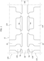
- Figure 1 illustrates the back/bottom surface of a portion of a leadframe strip 12 including portions of two neighboring (individual) leadframes or substrates for respective (integrated circuit) semiconductor devices, not visible in their entirety.
- leadframes or substrates are indicated with the reference 120 in the figures, e.g., in Figure 2 , which refers to a condition after singulation.
- leadframe (or “lead frame”) is currently used (see, for instance the USPC Consolidated Glossary of the United States Patent and Trademark Office) to indicate a metal frame that provides support for an integrated circuit chip or die as well as electrical leads to interconnect the integrated circuit in the die or chip (the terms chip/s and die/dice are regarded as synonymous) to other electrical components or contacts.
- a leadframe comprises an array of electrically-conductive formations (or leads, e.g., 12B) that from an outline location extend inwardly in the direction of a semiconductor chip or die thus forming an array of electrically-conductive formations from a die pad (e.g., 12A in Figure 1 ) configured to have at least one (integrated circuit) semiconductor chip or die attached on the top/front surface thereof. This may be via conventional means such as a die attach adhesive (a die attach film or DAF, for instance).
- a die attach adhesive a die attach film or DAF, for instance
- a leadframe can be of the pre-molded type, that is a type of leadframe comprising a sculptured metal (e.g., copper) structure formed by etching a metal sheet and comprising empty spaces that are filled by an insulating compound (a resin, for instance) "pre-molded" on the sculptured metal structure.
- a sculptured metal e.g., copper
- a resin a resin, for instance
- leadframes are arranged in a leadframe strip 12 and held together via sacrificial connecting bars CB running at the periphery of the individual leadframes 120.
- Leadframes 120 are connected to the connecting bars via so-called tie bars TB, bridge-like formations that connect the pads (e.g., 12A) or the leads (e.g., 12B) of a leadframe to the connecting bars.
- tie bars TB bridge-like formations that connect the pads (e.g., 12A) or the leads (e.g., 12B) of a leadframe to the connecting bars.
- Figure 1 illustrates the back/bottom surface of portions of a leadframe strip 12 after a plating step has been performed to plate a solderable metallic (e.g., tin) layer.
- the leadframe strip 12 of Figure 1 is intended to give rise to two (individual) adjacent/neighboring leadframes 120 as illustrated in Figure 2 in response to singulation.
- Singulation is performed after dice/chips are arranged on the top/front surface of the corresponding die mounting locations (e.g., the die pads 12A) and a plastic encapsulation is molded onto the assembly.
- the dice/chips are assumed to be arranged on the front or top surface of the leadframe strip 12/individual leadframes 120. Thus, they are not visible in figures such as Figures 1 and 2 , which are (plan) views of the back or bottom surface.
- the molding compound 20 of the encapsulation may be at least partly visible also on the back/bottom surface of the leadframe strip 12.
- an electrically conductive layer of, for example, tin may enhance solderability of the device onto support substrate like a printed circuit board (PCB), for instance.
- PCB printed circuit board
- the leadframe portion indicated with the reference 12A in Figure 1 and described throughout as a die pad may also be a power lead.
- leadframe portion indicated with the reference 12A in Figure 1 and described throughout as a die pad may also be a (power) output lead.
- a processing flow as consider so far may involve a plating step wherein the connecting bars CB are exposed (that is, left uncovered by the molding compound) at the back/bottom surface of the leadframe strip 12.
- connecting bars CB and tie bars TB are exposed during the plating step and are thus plated with a solderable metallic layer.
- connecting bars CB as exemplified in Figure 1 may be relatively large (e.g., wider than 200 microns). A fairly large amount of metal (e.g., tin) can thus accumulate on the bottom/back surface during the plating step.
- metal e.g., tin
- the leadframe strip 12 is cut (e.g., via a sawing blade B: for simplicity this is visible only in Figure 2 ) in order to singulate the strip into individual devices (with individual substrates/leadframes 120).
- the blade B cuts the connecting bars CB along their length (over a region having a width indicated as SW) thus removing the connecting bars CB as well as a portion of the tie bars TB connected thereto.
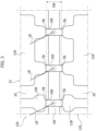
- Figure 2 illustrates the same portion of a leadframe strip 12 as exemplified in Figure 1 after sawing/cutting along the sawing width SW; the two adjacent/neighboring leadframes 120 are separated as a result of the removal of the connecting bars CB.
- Figure 2 (and Figures 3 and 4 as well) are thus again illustrative of a method where a plurality of semiconductor dice (chips) are arranged onto a first surface of a common electrically conductive substrate (e.g., a leadframe 12).
- a common electrically conductive substrate e.g., a leadframe 12
- the common substrate 12 has a second surface opposite the first surface and comprises adjacent substrate portions 120 having mutually facing sides with elongate sacrificial connecting bars CB extending therebetween.
- a solderable metallic layer (e.g., tin) is grown (e.g., plated) on the second surface of the common electrically conductive substrate 12 with the solderable metallic layer extending (also) over the connecting bars CB.
- filaments F of solderable metallic material may form starting from a die pad 12A (or from a lead 12B).
- such filaments or flakes F may undesirably establish electrical contact between neighboring electrically conductive formations such as die pads 12A or power lead 12B. This results in undesired electrical coupling (short-circuit) therebetween, which may cause failure (and rejection) of the final device.
- a possible conventional approach to counter filaments F formation involves reducing in as much as possible the thickness of the solderable metallic layer deposited on the back/bottom surface of the leadframe 12 during the plating step.
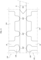
- filaments F formation of filaments F is countered by (selectively) removing the solderable metallic layer deposited on the back/bottom surface of the connecting bars CB, from at least part of the length the sacrificial connecting bars CB.
- removing the solderable metallic layer from the connecting bars CB may be advantageously limited to particular locations 100, namely at tie bars TB that are observed to provide "anchor points" for filament formation.
- the solderable metallic layer e.g., tin
- the solderable metallic layer may be advantageously removed at the locations 100 via laser ablation - as schematically indicated by reference LB - during an (additional) processing step that can be performed prior to the final singulation step.
- etching other techniques (e.g., etching) can be adopted to selectively remove the solderable metallic layer from the locations 100.
- filaments F formation of filaments F is thus countered in so far as (e.g., prior to the singulation step) the solderable metallic layer is removed from selected locations 100 of the connecting bars CB; the full thickness of the solderable metallic layer is removed, thus leaving uncovered, that is exposed, the metallic material of the leadframe strip 12 underneath.
- the solderable metallic layer may be tin and the leadframe 12 copper.
- copper will be exposed at the (ablated) regions 100, while the rest of the leadframe strip 12 will be covered with tin.
- Different materials or alloys may be used depending on application options.
- cutting the leadframe 12 providing (prior to singulation) a common electrically conductive substrate having the plurality of semiconductor dice arranged onto the first surface thereof to provide singulated individual semiconductor devices is (e.g., via the blade B over a width SW) along the length of the elongate sacrificial connecting bars CB having the solderable metallic layer removed from at least part of the length the sacrificial connecting bars CB.
- the solderable metallic layer is removed (e.g., via laser ablation LB) at selected locations 100 distributed along the length of the sacrificial connecting bars CB.
- solderable metallic layer can be removed from the sacrificial connecting bars CB at tie bars TB that couple the elongate sacrificial connecting bars (CB) to adjacent substrate portions 120 in the common electrically conductive substrate (leadframe 12).
- the regions 100 wherein the solderable metallic material has been removed may extend beyond the width of the connecting bars CB into the tie bars TB.
- the regions 100 may extend beyond the sawing width SW (in dashed lines in Figure 3 ).
- a singulation step may be performed, wherein the sacrificial connecting bars CB are removed (via sawing, for instance). Having removed the full thickness of the solderable metallic layer at regions 100, the blade will not contact the solderable metallic layer at the tie bars TB thus reducing (notionally eliminating) the risk of filament formation.
- a portion 100' of the regions wherein the solderable metallic layer has been removed may be left (and thus remain observable) at the surface of the individual leadframe of the final device and it will be visible on the bottom and side surfaces thereof.
- solderable metallic layer can be removed from the distal ends 100' of the tie bars TB that (in the leadframe 12 prior to singulation) couple the elongate sacrificial connecting bars CB to adjacent substrate portions 120 in the common electrically conductive substrate 12.
- solderable metallic material from the regions 100 of the connecting bars CB does not compromise the solderability of the final device; apart from the small portion 100' at the distal ends of the remainders of the tie bars TB, the bottom surface of the leadframes 120 is plated with a solderable metallic layer of a desired thickness.
- Such processing may result in a (final) singulated semiconductor device that comprises one or more semiconductor dice (or chips) arranged onto a first surface of a portion 120 of an electrically conductive substrate (such as a leadframe 12) having a second surface opposite the first surface with a solderable metallic layer grown on the second surface.
- an electrically conductive substrate such as a leadframe 12
- the respective portion (leadframe portion 120) of electrically conductive substrate comprises remainders of the tie bars (the distal ends 100') distributed along the length of and protruding from at least one side of that leadframe portion.
- the solderable metallic layer is absent from these remainders of tie bars 100' in so far as the solderable metallic layer was removed (e.g., laser ablated) from these distal ends 100'.
Landscapes
- Lead Frames For Integrated Circuits (AREA)
- Engineering & Computer Science (AREA)
- Manufacturing & Machinery (AREA)
- Physics & Mathematics (AREA)
- Geometry (AREA)
Abstract
Description
- The description relates to manufacturing semiconductor devices.
- Solutions as described herein can be applied to power integrated circuit (IC) semiconductor devices such as power QFN packages, for automotive or industrial products, for instance.
- In current manufacturing processes of (IC) semiconductor devices, multiple devices are concurrently processed and finally singulated into individual devices.
- During processing, a plurality of substrates (leadframes) for individual devices are held together in a leadframe strip using metallic connecting structures including (sacrificial) connecting bars running along the periphery of each device.
- Prior to the singulation step, a plating step can be performed in order to plate the leadframe bottom surface with a metallic (solderable) layer, of tin, for instance.
- Processing of certain devices may be facilitated by providing relatively large connecting bars (e.g., wider than 200 microns) that are exposed during the plating step. This results in the connecting bars being plated during the plating step with a fairly large amount of metal accumulated on the connecting bars.
- During the singulation step a blade is used to remove the connecting bars and the solderable metallic layer plated thereon. Due to the amount of metal accumulated on the connecting bars, the action of the blade during the singulation step may produce flakes or filaments that undesirably "bridge" neighboring leads causing a short circuit therebetween.
- Such an undesired electrical coupling (short) causes rejection and/or failure of the device.
- Documents
US 2022/384209 A1 ,US 2022/344173 A1 , andUS 2022/077086 A1 are exemplary of technical background of interest for the invention. - Solutions as described herein aim at addressing the issues discussed in the foregoing.
- Such an object can be achieved via a method having the features set forth in the claims that follow.
- One or more embodiments relate to a corresponding (integrated circuit) semiconductor device.
- The claims are an integral part of the technical teaching provided in respect of the embodiments.
- In solutions as described herein, a processing step is provided in order to counter filaments/flakes formation which could cause failure of the device.
- In solutions as described herein, metallic material accumulated on the back/bottom surface of the connecting bars during the plating step is removed before the singulation step in order to counter flakes/filaments formation.
- In solutions as described herein, metallic material may be removed from the back/bottom surface of the connecting bars via laser ablation.
- One or more embodiments will now be described, by way of example only, with reference to the annexed figures, wherein:
-
Figure 1 is a plan view illustrative of a portion of a leadframe strip, -
Figure 2 is a plan view illustrative of a final singulation step performed on the leadframe strip illustrated inFigure 1 , -
Figure 3 is a plan view illustrative of a portion of a leadframe strip processed according to embodiments of the present description, and -
Figure 4 is a plan view illustrative of a final singulation step performed on the leadframe strip illustrated inFigure 3 . - Corresponding numerals and symbols in the different figures generally refer to corresponding parts unless otherwise indicated.
- The figures are drawn to clearly illustrate the relevant aspects of the embodiments and are not necessarily drawn to scale.
- The edges of features drawn in the figures do not necessarily indicate the termination of the extent of the feature.
- In the ensuing description one or more specific details are illustrated, aimed at providing an in-depth understanding of examples of embodiments of this description. The embodiments may be obtained without one or more of the specific details, or with other methods, components, materials, etc. In other cases, known structures, materials, or operations are not illustrated or described in detail so that certain aspects of embodiments will not be obscured.
- Reference to "an embodiment" or "one embodiment" in the framework of the present description is intended to indicate that a particular configuration, structure, or characteristic described in relation to the embodiment is comprised in at least one embodiment. Hence, phrases such as "in an embodiment" or "in one embodiment" that may be present in one or more points of the present description do not necessarily refer to one and the same embodiment.
- Moreover, particular conformations, structures, or characteristics may be combined in any adequate way in one or more embodiments.
- The headings/references used herein are provided merely for convenience and hence do not define the extent of protection or the scope of the embodiments.
- For simplicity and ease of explanation, throughout this description, and unless the context indicates otherwise, like parts or elements are indicated in the various figures with like reference signs, and a corresponding description will not be repeated for each and every figure.
-
Figure 1 illustrates the back/bottom surface of a portion of aleadframe strip 12 including portions of two neighboring (individual) leadframes or substrates for respective (integrated circuit) semiconductor devices, not visible in their entirety. - These portions of leadframes or substrates are indicated with the
reference 120 in the figures, e.g., inFigure 2 , which refers to a condition after singulation. - In fact, in current manufacturing processes of (integrated circuit) semiconductor devices plural devices/leadframes are processed concurrently. Concurrent processing of a plurality of devices is achieved by providing a common substrate (e.g., a leadframe strip) comprising a plurality of individual substrate for each device.
- The designation "leadframe" (or "lead frame") is currently used (see, for instance the USPC Consolidated Glossary of the United States Patent and Trademark Office) to indicate a metal frame that provides support for an integrated circuit chip or die as well as electrical leads to interconnect the integrated circuit in the die or chip (the terms chip/s and die/dice are regarded as synonymous) to other electrical components or contacts.
- Essentially, a leadframe comprises an array of electrically-conductive formations (or leads, e.g., 12B) that from an outline location extend inwardly in the direction of a semiconductor chip or die thus forming an array of electrically-conductive formations from a die pad (e.g., 12A in
Figure 1 ) configured to have at least one (integrated circuit) semiconductor chip or die attached on the top/front surface thereof. This may be via conventional means such as a die attach adhesive (a die attach film or DAF, for instance). - In certain cases, a leadframe can be of the pre-molded type, that is a type of leadframe comprising a sculptured metal (e.g., copper) structure formed by etching a metal sheet and comprising empty spaces that are filled by an insulating compound (a resin, for instance) "pre-molded" on the sculptured metal structure.
- In order to concurrently process several devices, several leadframes are arranged in a
leadframe strip 12 and held together via sacrificial connecting bars CB running at the periphery of theindividual leadframes 120. -
Leadframes 120 are connected to the connecting bars via so-called tie bars TB, bridge-like formations that connect the pads (e.g., 12A) or the leads (e.g., 12B) of a leadframe to the connecting bars. - As known to those of skill in the art, current manufacturing processes of (integrated circuit, IC) semiconductor devices may involve:
- arranging one or more semiconductor (e.g., silicon) die on the top/front surface of a corresponding die mounting location (e.g., die
pads 12A), - providing electrical coupling between the die/dice and selected one of the
leads 12B via wire bonding or, as it is the case in power devices, via clips or ribbons, - molding an insulating molding compound (e.g., an epoxy resin) on the
leadframe strip 12 having the dice arranged on the top/front surface thereof to provide a protective plastic package to the devices, - a plating step wherein a solderable electrically conductive layer (e.g., a tin layer) is plated on the bottom/back surface of the
leadframes 12, and - a final singulation step wherein the processed
leadframe strip 12 is cut (e.g., via sawing) into individual devices (with individual leadframes 120). - The sequence of steps just described is merely exemplary insofar as, for example, additional processing steps may be envisaged.
- As noted, processing steps as described so far are otherwise conventional in the art, which makes it making unnecessary to provide a more detailed description herein.
- In various embodiments, other techniques (e.g., printing) can be adopted in the place of plating to provide a solderable metallic layer on the back or bottom surface of the
substrate 120. -
Figure 1 illustrates the back/bottom surface of portions of aleadframe strip 12 after a plating step has been performed to plate a solderable metallic (e.g., tin) layer. Theleadframe strip 12 ofFigure 1 is intended to give rise to two (individual) adjacent/neighboringleadframes 120 as illustrated inFigure 2 in response to singulation. - Singulation is performed after dice/chips are arranged on the top/front surface of the corresponding die mounting locations (e.g., the
die pads 12A) and a plastic encapsulation is molded onto the assembly. The dice/chips are assumed to be arranged on the front or top surface of theleadframe strip 12/individual leadframes 120. Thus, they are not visible in figures such asFigures 1 and2 , which are (plan) views of the back or bottom surface. Conversely, themolding compound 20 of the encapsulation may be at least partly visible also on the back/bottom surface of theleadframe strip 12. - As known to those skilled in the art, an electrically conductive layer of, for example, tin may enhance solderability of the device onto support substrate like a printed circuit board (PCB), for instance.
- In certain embodiments, the leadframe portion indicated with the
reference 12A inFigure 1 and described throughout as a die pad may also be a power lead. - This can be the case, for instance, of a power device, where the current(s) transferred from a (power) die to the power output leads of the device can be significant and leads with a larger contact area may be used for that purpose.
- Consequently, it will be understood that the leadframe portion indicated with the
reference 12A inFigure 1 and described throughout as a die pad may also be a (power) output lead. - A processing flow as consider so far may involve a plating step wherein the connecting bars CB are exposed (that is, left uncovered by the molding compound) at the back/bottom surface of the
leadframe strip 12. - In the case exemplified in
Figure 1 connecting bars CB and tie bars TB are exposed during the plating step and are thus plated with a solderable metallic layer. - Depending on the device design, connecting bars CB as exemplified in
Figure 1 may be relatively large (e.g., wider than 200 microns). A fairly large amount of metal (e.g., tin) can thus accumulate on the bottom/back surface during the plating step. - As discussed, after the plating step, the
leadframe strip 12 is cut (e.g., via a sawing blade B: for simplicity this is visible only inFigure 2 ) in order to singulate the strip into individual devices (with individual substrates/leadframes 120). - In the singulation step the blade B cuts the connecting bars CB along their length (over a region having a width indicated as SW) thus removing the connecting bars CB as well as a portion of the tie bars TB connected thereto.
-
Figure 2 illustrates the same portion of aleadframe strip 12 as exemplified inFigure 1 after sawing/cutting along the sawing width SW; the two adjacent/neighboringleadframes 120 are separated as a result of the removal of the connecting bars CB. -
Figure 2 (andFigures 3 and4 as well) are thus again illustrative of a method where a plurality of semiconductor dice (chips) are arranged onto a first surface of a common electrically conductive substrate (e.g., a leadframe 12). - The
common substrate 12 has a second surface opposite the first surface and comprisesadjacent substrate portions 120 having mutually facing sides with elongate sacrificial connecting bars CB extending therebetween. - A solderable metallic layer (e.g., tin) is grown (e.g., plated) on the second surface of the common electrically
conductive substrate 12 with the solderable metallic layer extending (also) over the connecting bars CB. - As a consequence of the action of the blade B and due to the amount of solderable metallic material plated on the back/bottom surface of the leadframes in the
leadframe strip 12, filaments F of solderable metallic material may form starting from adie pad 12A (or from a lead 12B). - As illustrated in
Figure 2 , such filaments or flakes F may undesirably establish electrical contact between neighboring electrically conductive formations such as diepads 12A orpower lead 12B. This results in undesired electrical coupling (short-circuit) therebetween, which may cause failure (and rejection) of the final device. - It is observed that formation of such filaments F is a major cause of rejection of when processing certain types of IC semiconductor devices.
- As discussed, a possible conventional approach to counter filaments F formation involves reducing in as much as possible the thickness of the solderable metallic layer deposited on the back/bottom surface of the
leadframe 12 during the plating step. - It is however noted that:
- the thickness of the solderable layer cannot be reduced beyond a certain limit as this would cause solderability issues when soldering the device to the final substrate (e.g., a PCB); and
- reducing the thickness of the solderable layer reduces formation of filaments F (thus leading to lower defect ratios), but does not provide a completely adequate solution to the problem of filament formation.
- In solutions as described herein, formation of filaments F is countered by (selectively) removing the solderable metallic layer deposited on the back/bottom surface of the connecting bars CB, from at least part of the length the sacrificial connecting bars CB.
- As illustrated in
Figure 3 , removing the solderable metallic layer from the connecting bars CB may be advantageously limited toparticular locations 100, namely at tie bars TB that are observed to provide "anchor points" for filament formation. - As exemplified in
Figure 3 , in solutions as described herein, the solderable metallic layer (e.g., tin) may be advantageously removed at thelocations 100 via laser ablation - as schematically indicated by reference LB - during an (additional) processing step that can be performed prior to the final singulation step. - In various embodiments, other techniques (e.g., etching) can be adopted to selectively remove the solderable metallic layer from the
locations 100. - In solutions as described herein, formation of filaments F is thus countered in so far as (e.g., prior to the singulation step) the solderable metallic layer is removed from selected
locations 100 of the connecting bars CB; the full thickness of the solderable metallic layer is removed, thus leaving uncovered, that is exposed, the metallic material of theleadframe strip 12 underneath. - In examples as considered herein, the solderable metallic layer may be tin and the
leadframe 12 copper. In these examples, copper will be exposed at the (ablated)regions 100, while the rest of theleadframe strip 12 will be covered with tin. Different materials or alloys may be used depending on application options. - In examples as considered herein, cutting the
leadframe 12 providing (prior to singulation) a common electrically conductive substrate having the plurality of semiconductor dice arranged onto the first surface thereof to provide singulated individual semiconductor devices is (e.g., via the blade B over a width SW) along the length of the elongate sacrificial connecting bars CB having the solderable metallic layer removed from at least part of the length the sacrificial connecting bars CB. - In examples as considered herein, the solderable metallic layer is removed (e.g., via laser ablation LB) at selected
locations 100 distributed along the length of the sacrificial connecting bars CB. - As illustrated, the solderable metallic layer can be removed from the sacrificial connecting bars CB at tie bars TB that couple the elongate sacrificial connecting bars (CB) to
adjacent substrate portions 120 in the common electrically conductive substrate (leadframe 12). - As illustrated in
Figure 3 , theregions 100 wherein the solderable metallic material has been removed may extend beyond the width of the connecting bars CB into the tie bars TB. In particular, as illustrated inFigure 3 , theregions 100 may extend beyond the sawing width SW (in dashed lines inFigure 3 ). - After removing the solderable metallic layer at
regions 100, a singulation step may be performed, wherein the sacrificial connecting bars CB are removed (via sawing, for instance). Having removed the full thickness of the solderable metallic layer atregions 100, the blade will not contact the solderable metallic layer at the tie bars TB thus reducing (notionally eliminating) the risk of filament formation. - As illustrated in
Figure 4 , a portion 100' of the regions wherein the solderable metallic layer has been removed may be left (and thus remain observable) at the surface of the individual leadframe of the final device and it will be visible on the bottom and side surfaces thereof. - That is, the solderable metallic layer can be removed from the distal ends 100' of the tie bars TB that (in the
leadframe 12 prior to singulation) couple the elongate sacrificial connecting bars CB toadjacent substrate portions 120 in the common electricallyconductive substrate 12. - It is noted that removing the solderable metallic material from the
regions 100 of the connecting bars CB does not compromise the solderability of the final device; apart from the small portion 100' at the distal ends of the remainders of the tie bars TB, the bottom surface of theleadframes 120 is plated with a solderable metallic layer of a desired thickness. - Such processing may result in a (final) singulated semiconductor device that comprises one or more semiconductor dice (or chips) arranged onto a first surface of a
portion 120 of an electrically conductive substrate (such as a leadframe 12) having a second surface opposite the first surface with a solderable metallic layer grown on the second surface. - In such a final singulated semiconductor device, the respective portion (leadframe portion 120) of electrically conductive substrate comprises remainders of the tie bars (the distal ends 100') distributed along the length of and protruding from at least one side of that leadframe portion. The solderable metallic layer is absent from these remainders of tie bars 100' in so far as the solderable metallic layer was removed (e.g., laser ablated) from these distal ends 100'.
- Without prejudice to the underlying principles, the details and embodiments may vary, even significantly, with respect to what has been described by way of example only without departing from the extent of protection. The extent of protection is determined by the annexed claims.
Claims (8)
- A method, comprising:arranging a plurality of semiconductor dice onto a first surface of a common electrically conductive substrate (12), wherein the common substrate (12) has a second surface opposite the first surface and comprises adjacent substrate portions (120) having mutually facing sides with elongate sacrificial connecting bars (CB) extending between adjacent mutually facing sides, with a solderable metallic layer grown on the second surface of the common electrically conductive substrate (12) the solderable metallic layer extending over the connecting bars (CB),removing the solderable metallic layer from at least part (100) of the length the sacrificial connecting bars (CB), andcutting (B, SW) the common electrically conductive substrate (12) having the plurality of semiconductor dice arranged onto the first surface thereof to provide singulated individual semiconductor devices, wherein cutting is along the length of the elongate sacrificial connecting bars (CB) having the solderable metallic layer removed from at least part (100) of the length the sacrificial connecting bars (CB).
- The method of claim 1, wherein the solderable metallic layer comprises tin.
- The method of claim 1 or claim 2, wherein the method comprises growing the solderable metallic layer on the second surface of the common electrically conductive substrate (12) via plating.
- The method of any of the previous claims, comprising removing the solderable metallic layer via laser ablation (LB).
- The method of any of the previous claims, comprising removing the solderable metallic layer at selected locations (100) distributed along the length the sacrificial connecting bars (CB).
- The method of claim 5, comprising removing the solderable metallic layer from the sacrificial connecting bars (CB) at tie bars (TB) coupling the elongate sacrificial connecting bars (CB) to adjacent substrate portions (120) in the common electrically conductive substrate (12).
- The method of claim 6, comprising removing the solderable metallic layer from distal ends (100') of the tie bars (TB) coupling the elongate sacrificial connecting bars (CB) to adjacent substrate portions (120) in the common electrically conductive substrate (12) .
- A semiconductor device obtainable with the method of claim 7, wherein the semiconductor device comprises at least one semiconductor die arranged onto a first surface of a portion (120) of an electrically conductive substrate (12) having a second surface opposite the first surface with a solderable metallic layer grown on the second surface, wherein the portion (120) of electrically conductive substrate (12) comprises remainders of tie bars (100') distributed along the length of and protruding from at least one side thereof, wherein the solderable metallic layer is absent from said remainders of tie bars (100').
Applications Claiming Priority (1)
| Application Number | Priority Date | Filing Date | Title |
|---|---|---|---|
| IT102023000006039A IT202300006039A1 (en) | 2023-03-29 | 2023-03-29 | PROCEDURE FOR MANUFACTURING SEMICONDUCTOR DEVICES AND CORRESPONDING SEMICONDUCTOR DEVICE |
Publications (2)
| Publication Number | Publication Date |
|---|---|
| EP4447094A1 true EP4447094A1 (en) | 2024-10-16 |
| EP4447094B1 EP4447094B1 (en) | 2026-04-29 |
Family
ID=86604588
Family Applications (1)
| Application Number | Title | Priority Date | Filing Date |
|---|---|---|---|
| EP24163133.2A Active EP4447094B1 (en) | 2023-03-29 | 2024-03-13 | A method of manufacturing semiconductor devices and corresponding semiconductor device |
Country Status (3)
| Country | Link |
|---|---|
| US (1) | US20240332250A1 (en) |
| EP (1) | EP4447094B1 (en) |
| IT (1) | IT202300006039A1 (en) |
Citations (3)
| Publication number | Priority date | Publication date | Assignee | Title |
|---|---|---|---|---|
| US20220077086A1 (en) | 2020-09-08 | 2022-03-10 | Panjit International Inc. | Side wettable package and method for manufacturing the same |
| US20220344173A1 (en) | 2021-04-26 | 2022-10-27 | Microchip Technology Incorporated | Method of forming a surface-mount integrated circuit package with solder enhanced leadframe terminals |
| US20220384209A1 (en) | 2021-06-01 | 2022-12-01 | Stmicroelectronics S.R.L. | Method of manufacturing semiconductor devices and corresponding semiconductor device |
-
2023
- 2023-03-29 IT IT102023000006039A patent/IT202300006039A1/en unknown
-
2024
- 2024-03-13 EP EP24163133.2A patent/EP4447094B1/en active Active
- 2024-03-25 US US18/615,039 patent/US20240332250A1/en active Pending
Patent Citations (3)
| Publication number | Priority date | Publication date | Assignee | Title |
|---|---|---|---|---|
| US20220077086A1 (en) | 2020-09-08 | 2022-03-10 | Panjit International Inc. | Side wettable package and method for manufacturing the same |
| US20220344173A1 (en) | 2021-04-26 | 2022-10-27 | Microchip Technology Incorporated | Method of forming a surface-mount integrated circuit package with solder enhanced leadframe terminals |
| US20220384209A1 (en) | 2021-06-01 | 2022-12-01 | Stmicroelectronics S.R.L. | Method of manufacturing semiconductor devices and corresponding semiconductor device |
Also Published As
| Publication number | Publication date |
|---|---|
| EP4447094B1 (en) | 2026-04-29 |
| IT202300006039A1 (en) | 2024-09-29 |
| US20240332250A1 (en) | 2024-10-03 |
Similar Documents
| Publication | Publication Date | Title |
|---|---|---|
| US6841414B1 (en) | Saw and etch singulation method for a chip package | |
| US6911353B2 (en) | Semiconductor device and method of manufacturing same | |
| US7348659B2 (en) | Semiconductor device and method of manufacturing thereof | |
| US20250054843A1 (en) | Leadframe, Encapsulated Package with Punched Lead and Sawn Side Flanks, and Corresponding Manufacturing Method | |
| CN103155136B (en) | Singulation of IC packages | |
| US9363901B2 (en) | Making a plurality of integrated circuit packages | |
| US8076181B1 (en) | Lead plating technique for singulated IC packages | |
| KR20030031843A (en) | Leadframe and method of manufacturing a semiconductor device using the same | |
| EP4379788A1 (en) | A method of manufacturing semiconductor devices and corresponding semiconductor device | |
| EP4447094B1 (en) | A method of manufacturing semiconductor devices and corresponding semiconductor device | |
| US20250105024A1 (en) | Method of manufacturing semiconductor devices and corresponding semiconductor device | |
| US11444012B2 (en) | Packaged electronic device with split die pad in robust package substrate | |
| US11631634B2 (en) | Leadless semiconductor package and method of manufacture | |
| EP4462467B1 (en) | Method of manufacturing semiconductor devices | |
| EP4489070A1 (en) | Method of manufacturing semiconductor devices, corresponding pre-molded leadframe and semiconductor device | |
| CN118737840A (en) | Method for manufacturing a semiconductor device and corresponding semiconductor device | |
| US20220270957A1 (en) | Quad flat no-lead (qfn) manufacturing process | |
| EP4383318A1 (en) | Method of manufacturing semiconductor devices, corresponding substrate and semiconductor device | |
| EP4312250A1 (en) | Method of manufacturing semiconductor devices, corresponding substrate and semiconductor device | |
| US20240178105A1 (en) | Method of manufacturing substrates for semiconductor devices, corresponding product and semiconductor device | |
| US12165880B2 (en) | Method of manufacturing semiconductor devices and corresponding semiconductor device | |
| TWI900363B (en) | Method for forming non-leaded semiconductor package device | |
| CN118173503A (en) | Method for manufacturing a semiconductor device, corresponding substrate and semiconductor device | |
| EP4451327A1 (en) | Method of manufacturing semiconductor devices, corresponding substrate and semiconductor device | |
| EP4542629A1 (en) | Method of manufacturing semiconductor devices and corresponding semiconductor device |
Legal Events
| Date | Code | Title | Description |
|---|---|---|---|
| PUAI | Public reference made under article 153(3) epc to a published international application that has entered the european phase |
Free format text: ORIGINAL CODE: 0009012 |
|
| STAA | Information on the status of an ep patent application or granted ep patent |
Free format text: STATUS: THE APPLICATION HAS BEEN PUBLISHED |
|
| AK | Designated contracting states |
Kind code of ref document: A1 Designated state(s): AL AT BE BG CH CY CZ DE DK EE ES FI FR GB GR HR HU IE IS IT LI LT LU LV MC ME MK MT NL NO PL PT RO RS SE SI SK SM TR |
|
| STAA | Information on the status of an ep patent application or granted ep patent |
Free format text: STATUS: REQUEST FOR EXAMINATION WAS MADE |
|
| 17P | Request for examination filed |
Effective date: 20250324 |
|
| GRAP | Despatch of communication of intention to grant a patent |
Free format text: ORIGINAL CODE: EPIDOSNIGR1 |
|
| STAA | Information on the status of an ep patent application or granted ep patent |
Free format text: STATUS: GRANT OF PATENT IS INTENDED |
|
| INTG | Intention to grant announced |
Effective date: 20251203 |
|
| GRAS | Grant fee paid |
Free format text: ORIGINAL CODE: EPIDOSNIGR3 |
|
| GRAA | (expected) grant |
Free format text: ORIGINAL CODE: 0009210 |
|
| STAA | Information on the status of an ep patent application or granted ep patent |
Free format text: STATUS: THE PATENT HAS BEEN GRANTED |
|
| AK | Designated contracting states |
Kind code of ref document: B1 Designated state(s): AL AT BE BG CH CY CZ DE DK EE ES FI FR GB GR HR HU IE IS IT LI LT LU LV MC ME MK MT NL NO PL PT RO RS SE SI SK SM TR |
|
| REG | Reference to a national code |
Ref country code: CH Ref legal event code: F10 Free format text: ST27 STATUS EVENT CODE: U-0-0-F10-F00 (AS PROVIDED BY THE NATIONAL OFFICE) Effective date: 20260429 Ref country code: GB Ref legal event code: FG4D |