EP4446806A1 - Display device - Google Patents
Display device Download PDFInfo
- Publication number
- EP4446806A1 EP4446806A1 EP22903003.6A EP22903003A EP4446806A1 EP 4446806 A1 EP4446806 A1 EP 4446806A1 EP 22903003 A EP22903003 A EP 22903003A EP 4446806 A1 EP4446806 A1 EP 4446806A1
- Authority
- EP
- European Patent Office
- Prior art keywords
- display device
- display
- display module
- bottom wall
- present disclosure
- Prior art date
- Legal status (The legal status is an assumption and is not a legal conclusion. Google has not performed a legal analysis and makes no representation as to the accuracy of the status listed.)
- Pending
Links
Images

Classifications
-
- H—ELECTRICITY
- H04—ELECTRIC COMMUNICATION TECHNIQUE
- H04N—PICTORIAL COMMUNICATION, e.g. TELEVISION
- H04N5/00—Details of television systems
- H04N5/64—Constructional details of receivers, e.g. cabinets or dust covers
-
- G—PHYSICS
- G02—OPTICS
- G02F—OPTICAL DEVICES OR ARRANGEMENTS FOR THE CONTROL OF LIGHT BY MODIFICATION OF THE OPTICAL PROPERTIES OF THE MEDIA OF THE ELEMENTS INVOLVED THEREIN; NON-LINEAR OPTICS; FREQUENCY-CHANGING OF LIGHT; OPTICAL LOGIC ELEMENTS; OPTICAL ANALOGUE/DIGITAL CONVERTERS
- G02F1/00—Devices or arrangements for the control of the intensity, colour, phase, polarisation or direction of light arriving from an independent light source, e.g. switching, gating or modulating; Non-linear optics
- G02F1/01—Devices or arrangements for the control of the intensity, colour, phase, polarisation or direction of light arriving from an independent light source, e.g. switching, gating or modulating; Non-linear optics for the control of the intensity, phase, polarisation or colour
- G02F1/13—Devices or arrangements for the control of the intensity, colour, phase, polarisation or direction of light arriving from an independent light source, e.g. switching, gating or modulating; Non-linear optics for the control of the intensity, phase, polarisation or colour based on liquid crystals, e.g. single liquid crystal display cells
- G02F1/133—Constructional arrangements; Operation of liquid crystal cells; Circuit arrangements
- G02F1/1333—Constructional arrangements; Manufacturing methods
- G02F1/133308—Support structures for LCD panels, e.g. frames or bezels
- G02F1/133314—Back frames
-
- G—PHYSICS
- G02—OPTICS
- G02F—OPTICAL DEVICES OR ARRANGEMENTS FOR THE CONTROL OF LIGHT BY MODIFICATION OF THE OPTICAL PROPERTIES OF THE MEDIA OF THE ELEMENTS INVOLVED THEREIN; NON-LINEAR OPTICS; FREQUENCY-CHANGING OF LIGHT; OPTICAL LOGIC ELEMENTS; OPTICAL ANALOGUE/DIGITAL CONVERTERS
- G02F1/00—Devices or arrangements for the control of the intensity, colour, phase, polarisation or direction of light arriving from an independent light source, e.g. switching, gating or modulating; Non-linear optics
- G02F1/01—Devices or arrangements for the control of the intensity, colour, phase, polarisation or direction of light arriving from an independent light source, e.g. switching, gating or modulating; Non-linear optics for the control of the intensity, phase, polarisation or colour
- G02F1/13—Devices or arrangements for the control of the intensity, colour, phase, polarisation or direction of light arriving from an independent light source, e.g. switching, gating or modulating; Non-linear optics for the control of the intensity, phase, polarisation or colour based on liquid crystals, e.g. single liquid crystal display cells
- G02F1/133—Constructional arrangements; Operation of liquid crystal cells; Circuit arrangements
- G02F1/1333—Constructional arrangements; Manufacturing methods
- G02F1/133308—Support structures for LCD panels, e.g. frames or bezels
- G02F1/133317—Intermediate frames, e.g. between backlight housing and front frame
-
- G—PHYSICS
- G02—OPTICS
- G02F—OPTICAL DEVICES OR ARRANGEMENTS FOR THE CONTROL OF LIGHT BY MODIFICATION OF THE OPTICAL PROPERTIES OF THE MEDIA OF THE ELEMENTS INVOLVED THEREIN; NON-LINEAR OPTICS; FREQUENCY-CHANGING OF LIGHT; OPTICAL LOGIC ELEMENTS; OPTICAL ANALOGUE/DIGITAL CONVERTERS
- G02F1/00—Devices or arrangements for the control of the intensity, colour, phase, polarisation or direction of light arriving from an independent light source, e.g. switching, gating or modulating; Non-linear optics
- G02F1/01—Devices or arrangements for the control of the intensity, colour, phase, polarisation or direction of light arriving from an independent light source, e.g. switching, gating or modulating; Non-linear optics for the control of the intensity, phase, polarisation or colour
- G02F1/13—Devices or arrangements for the control of the intensity, colour, phase, polarisation or direction of light arriving from an independent light source, e.g. switching, gating or modulating; Non-linear optics for the control of the intensity, phase, polarisation or colour based on liquid crystals, e.g. single liquid crystal display cells
- G02F1/133—Constructional arrangements; Operation of liquid crystal cells; Circuit arrangements
- G02F1/1333—Constructional arrangements; Manufacturing methods
- G02F1/133382—Heating or cooling of liquid crystal cells other than for activation, e.g. circuits or arrangements for temperature control, stabilisation or uniform distribution over the cell
- G02F1/133385—Heating or cooling of liquid crystal cells other than for activation, e.g. circuits or arrangements for temperature control, stabilisation or uniform distribution over the cell with cooling means, e.g. fans
-
- G—PHYSICS
- G02—OPTICS
- G02F—OPTICAL DEVICES OR ARRANGEMENTS FOR THE CONTROL OF LIGHT BY MODIFICATION OF THE OPTICAL PROPERTIES OF THE MEDIA OF THE ELEMENTS INVOLVED THEREIN; NON-LINEAR OPTICS; FREQUENCY-CHANGING OF LIGHT; OPTICAL LOGIC ELEMENTS; OPTICAL ANALOGUE/DIGITAL CONVERTERS
- G02F1/00—Devices or arrangements for the control of the intensity, colour, phase, polarisation or direction of light arriving from an independent light source, e.g. switching, gating or modulating; Non-linear optics
- G02F1/01—Devices or arrangements for the control of the intensity, colour, phase, polarisation or direction of light arriving from an independent light source, e.g. switching, gating or modulating; Non-linear optics for the control of the intensity, phase, polarisation or colour
- G02F1/13—Devices or arrangements for the control of the intensity, colour, phase, polarisation or direction of light arriving from an independent light source, e.g. switching, gating or modulating; Non-linear optics for the control of the intensity, phase, polarisation or colour based on liquid crystals, e.g. single liquid crystal display cells
- G02F1/133—Constructional arrangements; Operation of liquid crystal cells; Circuit arrangements
- G02F1/1333—Constructional arrangements; Manufacturing methods
- G02F1/133308—Support structures for LCD panels, e.g. frames or bezels
Definitions
- the present disclosure relates to the field of display technology, specifically to a display device.
- a display device is an electronic device that can display images, including televisions, monitors, and other types.
- optical components such as backlight components and liquid crystal screens in display devices need to be installed and fixed with backplanes and plastic middle frames.
- the structure of the electronic device is relatively complex because many parts are required to be assembled, resulting in high material cost and low assembly efficiency.
- the embodiment of the present disclosure provides a display device, which can simplify the installation and fixing structure of the optical component, reduce the material cost, and improve the assembly efficiency.
- the backplate comprises a bottom wall and a side wall thereon; an inner surface of the side wall is provided with a flange portion that is opposite to the bottom wall; the bottom wall and the side wall are enclosed to form an accommodating cavity, and the flange portion separates the accommodating cavity into the first accommodating portion and the second accommodating portion.
- the flange portion is bent along a direction close to the bottom wall to form a folding structure.
- the liquid crystal screen is arranged on one side surface of the folding structure far away from the backlight component, and the liquid crystal screen and the folding structure are bonded through an adhesive.
- a upper part of the flange portion facing the bottom wall has a plane structure.
- the folding edge structure is left with a gap.
- one side of the flange facing the bottom wall is provided with a protective layer which is made of a Mylar sheet, a plastic layer, a rubber layer and a sponge layer.
- one side of the flange facing the bottom wall is provided with a protective layer which is made of a Mylar sheet, a plastic layer, a rubber layer and a sponge layer.
- a thickness of the protective layer ranges between 0.2 and 0.5mm.
- the display module has a display surface and a back surface that are relatively arranged; the back side of the display module is provided with a plurality of device mounting areas; the display device comprises a plurality of back shells correspondingly arranged in the plurality of device mounting areas; each of the back shells is provided with a device mounting portion, and the back shells and the device mounting area are enclosed to form a device mounting cavity.
- the plurality of device mounting areas are defined on one side of the backplate far away from the display surface.
- the plurality of device mounting areas are arranged in the downside area of the display module along its height direction, and the plurality of device mounting areas are sequentially arranged along a width direction of the display module.
- one side edge of the back shell and the lower edge of the display module along its height direction are flush.
- the surface of one side of the back shell, far away from the display surface, and the back surface of the display module are shared in a plane or a curved surface.
- the display device further comprises a side frame, wherein the display module has a periphery surface connecting the display surface and the back surface, and the side frame is arranged on a periphery of the display module and an edge of the display surface.
- the side frame is only arranged in a local area on the periphery of the display module.
- the back shell and the side frame are buckled and connected.
- the display device further comprises a driving circuit arranged on the periphery of the display module and a heat-dissipating sheet arranged between the driving circuit and the side frame.
- the heat-dissipating sheet is made of a heat-dissipating material selected from at least one of a graphite sheet, a graphene film, a thermally conductive coating material, a ceramic material, a thermally conductive gel, and a phase-change material (PCM).
- a heat-dissipating material selected from at least one of a graphite sheet, a graphene film, a thermally conductive coating material, a ceramic material, a thermally conductive gel, and a phase-change material (PCM).
- the backlight component comprises a backlight source on the backplate, and an optical film on one side of the backlight that is far away from the backplate.
- the embodiment of the disclosure discloses a first accommodating portion and a second accommodating portion that are arranged in layers and communicating with each other on the backplate, accommodating a backlight component by the first accommodating portion, accommodating a liquid crystal screen by accommodating a second accommodating portion;
- the assembly efficiency is increased, and the surface material of the display device is more consistent, which increases the appearance consistency.
- 1- display device 10-display module, 11-backplane, 111-bottom wall, 112-flange portion, 113-side wall, 114-rear surface, 115-device mounting area, 11a-first accommodating portion, 11b-second accommodating portion, 12-backlight component, 121-backlight source, 122-optical film, 13-liquid crystal screen, 131-display surface, 14-protective layer, 20-back shell, 30-side frame, 41-driving circuit, 40-heat-dissipating sheet layer, 50-motherboard, 60-power supply, 70-speaker, 80-adhesive
- first and second are used for descriptive purposes only and should not be construed as indicating or implying relative importance or implying the number of technical features indicated.
- the features that are defined as “first” and “second” may explicitly or implicitly include one or more of the features described.
- “multiple” means two or more people, unless otherwise expressly and specifically qualified.
- a and/or B includes the following three combinations: A only, B only, and a combination of A and B.
- the term "exemplary” is used to mean “to be used as an example, illustration or illustration”. Any embodiment described as “exemplary” in this disclosure is not necessarily construed as being superior or superior to the other embodiments.
- the following description is given. In the following description, details are listed for the purpose of interpretation. It should be understood that a person of ordinary skill in the art can recognize that the present disclosure can be realized without the use of these specific details. In other cases, the structure and process of the public knowledge will not be elaborated in order to avoid unnecessary details obscure the description of this disclosure. Therefore, the present disclosure is not intended to be limited to the embodiments shown, but is consistent with the widest possible scope of the principles and characteristics disclosed in the present disclosure.
- the embodiment of the present disclosure provides a display device 1.
- the display device 1 having a display module 10 can simplify the installation and fixing structure of optical components such as backlight component, liquid crystal screen, etc., reduce material cost, improve assembly efficiency.
- the display device 1 may be determined according to actual needs.
- the display device 1 may be but not limited to a television, a display, etc.
- the display module 10 comprises a backplane 11, a backlight component 12 and a liquid crystal screen 13.
- the backplane 11 includes a first accommodating portion 11a and a second accommodating portion 11b that are arranged in layers and communicated with each other on one side.
- the first accommodating portion 11a is configured to accommodate the backlight component 12, and the second accommodating portion 11b is configured to accommodate the liquid crystal screen 13.
- the backplane 11 is an integral structure and includes the first accommodating portion 11a and the second accommodating portion 11b. In this way, under the condition of not adopting plastic middle frame, the installation and fixation of optical components such as backlight component 12 and the liquid crystal screen 13 can be realized by using the backplane 11 of integrated arrangement.
- the backplate 11 may be decided according to actual needs, and the embodiments of the present disclosure are not limited to this.
- the backplate 11 may comprise a bottom wall 111 and a side wall 113 thereon.
- An inner surface of the side wall 113 is provided with a flange portion 112 arranged relative to the bottom wall 111.
- the bottom wall 111 and the side wall 113 are enclosed to form an accommodating cavity.
- the flange portion 112 separates the accommodating cavity into the first accommodating portion 11a and the second accommodating portion 11b.
- the first accommodating portion 11a is defined by the bottom wall 111, the flange portion 112 and the side wall 113, while the second accommodating portion 11b is defined by the flange portion 112 away from the bottom wall 111 and the side wall 113.
- the bottom wall 111, the side wall 113 and the flange section 112 may be made in one piece by a one-piece molding process or by the welding/bonding process. In this way, the backlight component 12 can be reliably arranged in the first accommodating portion 11a.
- the rear side of the backlight component 12 is supported and protected by the bottom wall 111 of the backplate 11, the front side of the backlight component 12 is supported and protected by the flange portion 112, and the circumferential side of the backlight component 12 is supported and protected by the side wall 113, so that the backlight component 12 is not easy to damage and has high safety.
- the liquid crystal screen 13 can be reliably arranged in the second accommodating portion 11b, and the rear side of the liquid crystal screen 13 can be supported and protected by the flange portion 112, the circumferential side of the liquid crystal screen 13 can be protected by the side wall 113.
- the backlight component 12 may comprise a backlight source 121 and an optical film 122.
- the backlight source 121 may be arranged on the backplane 11
- the optical film 122 may be arranged on one side of the backlight source 121 that is far away from the backplane 11.
- the flange portion 112 may be bent close to the bottom wall 111 to form a flanging structure.
- the liquid crystal screen 13 can be arranged on one side surface of the flanging structure away from the backlight component 12. In this way, the liquid crystal screen 13 can get the reliable support and good positioning of the folding edge structure.
- the liquid crystal screen 13 can be adhesived and fixed between the folding structure, so that the liquid crystal screen 13 can be reliably installed.
- a containment groove portion defined by the flange portion 112 located at each side may fit the liquid crystal screen 13 and support the liquid crystal screen 13.
- the liquid crystal screen 13 and the folding structure can be bonded by adhesive 80.
- the flange subpart of the flange portion 112 facing the bottom wall 111 may be a flat structure, which is easy to carry out mass production and reduce manufacturing costs.
- Whether there is a gap when the folding structure is bent may be decided according to actual needs, and the embodiment of the present disclosure does not limit this. As shown in Fig. 3 , when the expansion and contraction of the backlight component 12 changes greatly, the folding structure can leave the gap to meet the thermal expansion space needs of the backlight component 12 and avoid the collision damage of the backlight component 12 during expansion.
- one side of the flange portion 112 facing the bottom wall 111 may be provided with a protective layer 14 which may be made of a Mylar sheet, plastic layer, rubber layer or sponge layer.
- a protective layer 14 which may be made of a Mylar sheet, plastic layer, rubber layer or sponge layer.
- the protective layer 14 can buffer the backlight component 12 to avoid the backlight component 12 from being worn or scratched by the flange portion 112.
- a thickness of the protective layer 14 may be determined according to actual needs, and the embodiments of the present disclosure do not limit this.
- the thickness of the protective layer 14 may range 0.2-0.5mm, such as 0.2mm, 0.25mm, 0.3mm, 0.35mm, 0.4mm, 0.45mm or 0.5mm, etc. In this thickness range, the protective layer 14 is thinner and has sufficient cushioning protection.
- the display unit is usually provided with only a monolithic back shell.
- components such as a motherboard, power supply, speaker
- the back shell aims the corresponding position on the display module to cover and protect these devices.
- the installation of components such as motherboard, power supply, and speaker, as well as the installation of the back shell, need to be concentrated in the assembly link of the whole machine involving the display module, resulting in a complicated and lengthy assembly process and low assembly efficiency.
- the display device 1 may also include a plurality of back shells 20.
- the display module 10 has a display surface 131 and a rear surface 114 that are relative to each other.
- the display surface 131 is used to display images.
- the rear surface 114 of the display module 10 is provided with a plurality of device mounting areas 115, and each device installation area 115 can be configured to install at least one device.
- the type of device can be determined according to the actual needs, and can include the motherboard 50, the power supply 60, and the speaker 70.
- a plurality of backshells 20 correspondingly are arranged in a plurality of device mounting areas 115, so that each device mounting area 115 can be covered by a backshell 20, and backshells 20 and its corresponding device mounting areas 115 are enclosed to form a device mounting cavity.
- the backshell 20 is provided with a device mounting section, and the device mounting section can be configured to mount at least one device. In this way, the aforesaid device can be mounted on the corresponding back shell 20 first, and then the subsequent shell 20 is installed together with the rear surface 114 of the display module 10.
- the display device 1 provided in the present disclosure adopts a plurality of backshells 20; in this way, a plurality of component installation processes can be arranged, and the required devices such as motherboard 50, power supply 60, speaker 70 are pre-installed to the device installation portion of corresponding backshell 20, and then each backshell 20 that has been installed with corresponding devices is installed to the corresponding device installation area 115 when the whole machine is assembled, so that the rationality of the installation process is increased, and the whole machine assembly process is simplified.
- the component installation process and the whole machine installation process are relatively simple, so that the proficiency and efficiency of the assembly personnel of the corresponding process can be guaranteed, so as to improve the assembly efficiency of the whole machine.
- the setting position of the device mounting area 115 on the display module 10 may be determined according to actual needs, and the embodiments of the present disclosure do not limit this.
- the device mounting area 115 may be formed on the side of the backplane 11 away from the display surface 131.
- a plurality of device mounting areas 115 may be arranged in the downside area of the display module 10 along its height direction, and a plurality of device mounting areas 115 are sequentially arranged along the width direction of the display module 10.
- the lower side area of the display module 10 is more spacious, and the aforesaid device is arranged in the lower side area of the display module 10, so that the space utilization efficiency can be improved, the thickness of the display device 1 can be avoided from increasing significantly, and the display device 1 has a thinner effect.
- one side edge of the back shell 20 is flush with the lower edge of the display module 10 along its height direction. In this way, the display device 1 can be made to have a relatively flat lower side edge, and the overall layout is relatively neat.
- the surface of one side of the back shell 20, which is far away from the display surface 131, can be on a plane or a curved surface with the rear surface 114 of the display module 10. In this way, the back shell 20 as a whole can not be protruded from the rear surface 114 of the display module 10, on the one hand, the back shell 20 is avoided to hinder the heat dissipation of the display module 10, and the rear surface 114 of the display device 1 can be guaranteed on the other hand, and the appearance structure is neat, and it has a better appearance effect.
- the display device 1 may also include a side frame 30.
- the display module 10 has a periphery surface connecting the display surface 131 and the back surface 114.
- the side frame 30 can be arranged on the periphery surface of the display module 10 and at the edge of the display surface 131.
- the side frame 30 can structurally support and protect the display module 10 to form a part of the appearance of the display device 1.
- the side frame 30 can be connected to the back shell 20.
- the side frame 30 can be set only in a local area on the periphery surface of the display module 10.
- the display device 1 may also comprise a driving circuit 41 and a heat-dissipating sheet 40.
- the driving circuit 41 can be arranged on the display module 10 and is configured to drive the display module 10 to display images.
- the driving circuit 41 can be an integrated circuit chip (IC).
- the heat-dissipating sheet 40 is arranged between the driving circuit 41 and the side frame 30. The heat generated when the driving circuit 41 is working is dissipated, so that the driving circuit 41 is kept in a better temperature range.
- the heat-dissipating sheet 40 can be made of a vaporizing material which may be selected from one or more of graphite sheets, graphene films, thermally conductive coating materials, ceramic materials, thermally conductive gels, and phase change materials.
- the display device 1 provided in the embodiment of the present disclosure adopts a heat-dissipating sheet 40 for heat dissipation, and the thickness of the heat chamber layer 40 is thinner, so that the size of the display device 1 in the height direction can be avoided from being significantly increased, and the size of the side frame 30 in the height direction of the display device 1 is compressed, so as to save space and increase the screen-to-body ratio.
- the back shell 20 and the side frame 30 can be connected by snapping.
- the back shell 20 can be provided with the male buckle part
- the side frame 30 can be provided with the female buckle part.
- the male buckle part and the female buckle part are connected with the buckle and make the back shell 20 fixed.
- the rear shell 20 can be provided with the female buckle part
- the side frame 30 can be provided with the male buckle part
- the female buckle part and the male buckle part are connected with the buckle and make the back shell 20 fixed.
Landscapes
- Physics & Mathematics (AREA)
- Nonlinear Science (AREA)
- Mathematical Physics (AREA)
- Chemical & Material Sciences (AREA)
- Crystallography & Structural Chemistry (AREA)
- General Physics & Mathematics (AREA)
- Optics & Photonics (AREA)
- Engineering & Computer Science (AREA)
- Multimedia (AREA)
- Signal Processing (AREA)
- Devices For Indicating Variable Information By Combining Individual Elements (AREA)
- Liquid Crystal (AREA)
Abstract
Description
- This application claims priority to
Chinese Application No. 202123109871.1, entitled "DISPLAY DEVICE", filed on December 10, 2021 - The present disclosure relates to the field of display technology, specifically to a display device.
- A display device is an electronic device that can display images, including televisions, monitors, and other types.
- In related technologies, optical components such as backlight components and liquid crystal screens in display devices need to be installed and fixed with backplanes and plastic middle frames. The structure of the electronic device is relatively complex because many parts are required to be assembled, resulting in high material cost and low assembly efficiency.
- The embodiment of the present disclosure provides a display device, which can simplify the installation and fixing structure of the optical component, reduce the material cost, and improve the assembly efficiency.
- In some embodiments of the present disclosure, In some embodiments of the present disclosure, the backplate comprises a bottom wall and a side wall thereon; an inner surface of the side wall is provided with a flange portion that is opposite to the bottom wall; the bottom wall and the side wall are enclosed to form an accommodating cavity, and the flange portion separates the accommodating cavity into the first accommodating portion and the second accommodating portion.
- In some embodiments of the present disclosure, the flange portion is bent along a direction close to the bottom wall to form a folding structure.
- In some embodiments of the present disclosure, the liquid crystal screen is arranged on one side surface of the folding structure far away from the backlight component, and the liquid crystal screen and the folding structure are bonded through an adhesive.
- In some embodiments of the present disclosure, a upper part of the flange portion facing the bottom wall has a plane structure.
- In some embodiments of the present disclosure, the folding edge structure is left with a gap.
- In some embodiments of the present disclosure, one side of the flange facing the bottom wall is provided with a protective layer which is made of a Mylar sheet, a plastic layer, a rubber layer and a sponge layer.
- In some embodiments of the present disclosure, one side of the flange facing the bottom wall is provided with a protective layer which is made of a Mylar sheet, a plastic layer, a rubber layer and a sponge layer.
- In some embodiments of the present disclosure, a thickness of the protective layer ranges between 0.2 and 0.5mm.
- In some embodiments of the present disclosure, the display module has a display surface and a back surface that are relatively arranged; the back side of the display module is provided with a plurality of device mounting areas; the display device comprises a plurality of back shells correspondingly arranged in the plurality of device mounting areas; each of the back shells is provided with a device mounting portion, and the back shells and the device mounting area are enclosed to form a device mounting cavity.
- In some embodiments of the present disclosure, the plurality of device mounting areas are defined on one side of the backplate far away from the display surface.
- In some embodiments of the present disclosure, the plurality of device mounting areas are arranged in the downside area of the display module along its height direction, and the plurality of device mounting areas are sequentially arranged along a width direction of the display module.
- In some embodiments of the present disclosure, one side edge of the back shell and the lower edge of the display module along its height direction are flush.
- In some embodiments of the present disclosure, the surface of one side of the back shell, far away from the display surface, and the back surface of the display module are shared in a plane or a curved surface.
- In some embodiments of the present disclosure, the display device further comprises a side frame, wherein the display module has a periphery surface connecting the display surface and the back surface, and the side frame is arranged on a periphery of the display module and an edge of the display surface.
- In some embodiments of the present disclosure, the side frame is only arranged in a local area on the periphery of the display module.
- In some embodiments of the present disclosure, the back shell and the side frame are buckled and connected.
- In some embodiments of the present disclosure, the display device further comprises a driving circuit arranged on the periphery of the display module and a heat-dissipating sheet arranged between the driving circuit and the side frame.
- In some embodiments of the present disclosure, the heat-dissipating sheet is made of a heat-dissipating material selected from at least one of a graphite sheet, a graphene film, a thermally conductive coating material, a ceramic material, a thermally conductive gel, and a phase-change material (PCM).
- In some embodiments of the present disclosure, the backlight component comprises a backlight source on the backplate, and an optical film on one side of the backlight that is far away from the backplate.
- The embodiment of the disclosure discloses a first accommodating portion and a second accommodating portion that are arranged in layers and communicating with each other on the backplate, accommodating a backlight component by the first accommodating portion, accommodating a liquid crystal screen by accommodating a second accommodating portion; The assembly efficiency is increased, and the surface material of the display device is more consistent, which increases the appearance consistency.
- In order to more clearly illustrate the technical solutions in the embodiments of the present disclosure, the drawings required to be used in the description of the embodiments will be briefly introduced below, and it is obvious that the drawings described below are only some embodiments of the present disclosure, and for those skilled in the art, other drawings can be obtained according to these drawings without creative labor.
-
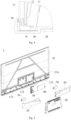
Fig. 1 is a local explosion structure diagram of the display device provided by some embodiments of the present disclosure; -
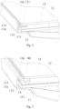
Fig. 2 is a partial cross-sectional structure diagram of the display device provided by some embodiments of the present disclosure; -
Fig. 3 is another partial cross-sectional structure diagram of the display device provided by some embodiments of the present disclosure; -
Fig. 4 is another partial cross-sectional structure diagram of the display device provided by some embodiments of the present disclosure; -
Fig. 5 is an overall explosion structure diagram of the display device provided by some embodiments of the present disclosure; -
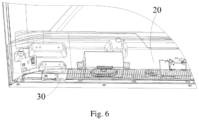
Fig. 6 is a partial perspective structure diagram of the display device provided by some embodiments of the present disclosure. - 1- display device, 10-display module, 11-backplane, 111-bottom wall, 112-flange portion, 113-side wall, 114-rear surface, 115-device mounting area, 11a-first accommodating portion, 11b-second accommodating portion, 12-backlight component, 121-backlight source, 122-optical film, 13-liquid crystal screen, 131-display surface, 14-protective layer, 20-back shell, 30-side frame, 41-driving circuit, 40-heat-dissipating sheet layer, 50-motherboard, 60-power supply, 70-speaker, 80-adhesive
- The technical solutions in the embodiments of the present disclosure will be clearly and completely described below in conjunction with the accompanying drawings in the embodiments of the present disclosure. It is obvious that the embodiments described are only part of the embodiments of the present disclosure, not all embodiments. Based on the embodiments in the present disclosure, all other embodiments obtained by a person skilled in the art without creative work fall within the scope of protection of the present disclosure.
- In the description of the present disclosure, it is understood that the terms "center", "longitudinal", "horizontal", "length", "width", "thickness", "up", "down", "front", "rear", "left", "right", "vertical", "horizontal", "top", "bottom", "inner", "outer", etc., indicate orientations or positional relationships based on the orientations or positional relationships shown in the drawings and are for the convenience of description and simplification of the description, and do not indicate or imply that the apparatus or elements referred to must have a specific orientation, It is constructed and operated in a specific direction, and therefore cannot be construed as a restriction on this disclosure. In addition, the terms "first" and "second" are used for descriptive purposes only and should not be construed as indicating or implying relative importance or implying the number of technical features indicated. Thus, the features that are defined as "first" and "second" may explicitly or implicitly include one or more of the features described. In the description of this disclosure, "multiple" means two or more people, unless otherwise expressly and specifically qualified.
- "A and/or B" includes the following three combinations: A only, B only, and a combination of A and B.
- The phrase "suitable for" or "configured to" in the present disclosure implies open and inclusive language, which does not exclude devices that are applicable to or configured to perform additional tasks or steps. In addition, the use of "based on" implies openness and inclusiveness, since a process, step, calculation or other action "based on" one or more of the stated conditions or values can in practice be based on additional conditions or beyond the stated values.
- In this disclosure, the term "exemplary" is used to mean "to be used as an example, illustration or illustration". Any embodiment described as "exemplary" in this disclosure is not necessarily construed as being superior or superior to the other embodiments. In order to enable any person skilled in the art to realize and use the present disclosure, the following description is given. In the following description, details are listed for the purpose of interpretation. It should be understood that a person of ordinary skill in the art can recognize that the present disclosure can be realized without the use of these specific details. In other cases, the structure and process of the public knowledge will not be elaborated in order to avoid unnecessary details obscure the description of this disclosure. Therefore, the present disclosure is not intended to be limited to the embodiments shown, but is consistent with the widest possible scope of the principles and characteristics disclosed in the present disclosure.
- As shown in
Fig. 1-Fig. 3 , the embodiment of the present disclosure provides adisplay device 1. Thedisplay device 1 having adisplay module 10 can simplify the installation and fixing structure of optical components such as backlight component, liquid crystal screen, etc., reduce material cost, improve assembly efficiency. Thedisplay device 1 may be determined according to actual needs. Thedisplay device 1 may be but not limited to a television, a display, etc. - The
display module 10 comprises abackplane 11, abacklight component 12 and aliquid crystal screen 13. Thebackplane 11 includes a firstaccommodating portion 11a and a secondaccommodating portion 11b that are arranged in layers and communicated with each other on one side. The firstaccommodating portion 11a is configured to accommodate thebacklight component 12, and the secondaccommodating portion 11b is configured to accommodate theliquid crystal screen 13. Thebackplane 11 is an integral structure and includes the firstaccommodating portion 11a and the secondaccommodating portion 11b. In this way, under the condition of not adopting plastic middle frame, the installation and fixation of optical components such asbacklight component 12 and theliquid crystal screen 13 can be realized by using thebackplane 11 of integrated arrangement. Since the number of parts is reduced, and the installation and fixing structure of optical components are simplified due to canceling plastic middle frame, material cost decreases and assembly efficiency is improved. In addition, compared with the inconsistency of the appearance materials caused by the use of a metal backplate and a plastic middle frame to form a shell in the related art, a better appearance consistency and integrity of thedisplay device 1 is visible because only thebackplate 11 is used without any plastic middle frame as the shell. - The structure of the
backplate 11 may be decided according to actual needs, and the embodiments of the present disclosure are not limited to this. In some embodiments, thebackplate 11 may comprise abottom wall 111 and aside wall 113 thereon. An inner surface of theside wall 113 is provided with aflange portion 112 arranged relative to thebottom wall 111. Thebottom wall 111 and theside wall 113 are enclosed to form an accommodating cavity. Theflange portion 112 separates the accommodating cavity into the firstaccommodating portion 11a and the secondaccommodating portion 11b. In other words, the firstaccommodating portion 11a is defined by thebottom wall 111, theflange portion 112 and theside wall 113, while the secondaccommodating portion 11b is defined by theflange portion 112 away from thebottom wall 111 and theside wall 113. Thebottom wall 111, theside wall 113 and theflange section 112 may be made in one piece by a one-piece molding process or by the welding/bonding process. In this way, thebacklight component 12 can be reliably arranged in the firstaccommodating portion 11a. The rear side of thebacklight component 12 is supported and protected by thebottom wall 111 of thebackplate 11, the front side of thebacklight component 12 is supported and protected by theflange portion 112, and the circumferential side of thebacklight component 12 is supported and protected by theside wall 113, so that thebacklight component 12 is not easy to damage and has high safety. Theliquid crystal screen 13 can be reliably arranged in the secondaccommodating portion 11b, and the rear side of theliquid crystal screen 13 can be supported and protected by theflange portion 112, the circumferential side of theliquid crystal screen 13 can be protected by theside wall 113. For example, thebacklight component 12 may comprise abacklight source 121 and anoptical film 122. Thebacklight source 121 may be arranged on thebackplane 11, and theoptical film 122 may be arranged on one side of thebacklight source 121 that is far away from thebackplane 11. - In some embodiments, the
flange portion 112 may be bent close to thebottom wall 111 to form a flanging structure. Theliquid crystal screen 13 can be arranged on one side surface of the flanging structure away from thebacklight component 12. In this way, theliquid crystal screen 13 can get the reliable support and good positioning of the folding edge structure. For example, theliquid crystal screen 13 can be adhesived and fixed between the folding structure, so that theliquid crystal screen 13 can be reliably installed. A containment groove portion defined by theflange portion 112 located at each side may fit theliquid crystal screen 13 and support theliquid crystal screen 13. Theliquid crystal screen 13 and the folding structure can be bonded byadhesive 80. For example, the flange subpart of theflange portion 112 facing thebottom wall 111 may be a flat structure, which is easy to carry out mass production and reduce manufacturing costs. - Whether there is a gap when the folding structure is bent may be decided according to actual needs, and the embodiment of the present disclosure does not limit this. As shown in
Fig. 3 , when the expansion and contraction of thebacklight component 12 changes greatly, the folding structure can leave the gap to meet the thermal expansion space needs of thebacklight component 12 and avoid the collision damage of thebacklight component 12 during expansion. - In some embodiments, one side of the
flange portion 112 facing thebottom wall 111 may be provided with aprotective layer 14 which may be made of a Mylar sheet, plastic layer, rubber layer or sponge layer. In this way, when thebacklight component 12 is arranged in the firstaccommodating portion 11a between theflange portion 112 and thebottom wall 111, theprotective layer 14 can buffer thebacklight component 12 to avoid thebacklight component 12 from being worn or scratched by theflange portion 112. A thickness of theprotective layer 14 may be determined according to actual needs, and the embodiments of the present disclosure do not limit this. For example, the thickness of theprotective layer 14 may range 0.2-0.5mm, such as 0.2mm, 0.25mm, 0.3mm, 0.35mm, 0.4mm, 0.45mm or 0.5mm, etc. In this thickness range, theprotective layer 14 is thinner and has sufficient cushioning protection. - In related art, the display unit is usually provided with only a monolithic back shell. In the assembly process of the display device, components, such as a motherboard, power supply, speaker, are required to be directly installed on corresponding areas on the back of the display module. Then the back shell aims the corresponding position on the display module to cover and protect these devices. In this way, the installation of components such as motherboard, power supply, and speaker, as well as the installation of the back shell, need to be concentrated in the assembly link of the whole machine involving the display module, resulting in a complicated and lengthy assembly process and low assembly efficiency.
- As shown in
Fig. 1- Fig. 6 , in some embodiments, thedisplay device 1 may also include a plurality ofback shells 20. Thedisplay module 10 has adisplay surface 131 and arear surface 114 that are relative to each other. Thedisplay surface 131 is used to display images. Therear surface 114 of thedisplay module 10 is provided with a plurality ofdevice mounting areas 115, and eachdevice installation area 115 can be configured to install at least one device. The type of device can be determined according to the actual needs, and can include themotherboard 50, thepower supply 60, and thespeaker 70. - A plurality of
backshells 20 correspondingly are arranged in a plurality ofdevice mounting areas 115, so that eachdevice mounting area 115 can be covered by abackshell 20, and backshells 20 and its correspondingdevice mounting areas 115 are enclosed to form a device mounting cavity. Thebackshell 20 is provided with a device mounting section, and the device mounting section can be configured to mount at least one device. In this way, the aforesaid device can be mounted on the corresponding backshell 20 first, and then thesubsequent shell 20 is installed together with therear surface 114 of thedisplay module 10. - Compared with related technologies, the
display device 1 provided in the present disclosure adopts a plurality ofbackshells 20; in this way, a plurality of component installation processes can be arranged, and the required devices such asmotherboard 50,power supply 60,speaker 70 are pre-installed to the device installation portion of correspondingbackshell 20, and then each backshell 20 that has been installed with corresponding devices is installed to the correspondingdevice installation area 115 when the whole machine is assembled, so that the rationality of the installation process is increased, and the whole machine assembly process is simplified. The component installation process and the whole machine installation process are relatively simple, so that the proficiency and efficiency of the assembly personnel of the corresponding process can be guaranteed, so as to improve the assembly efficiency of the whole machine. - The setting position of the
device mounting area 115 on thedisplay module 10 may be determined according to actual needs, and the embodiments of the present disclosure do not limit this. In some embodiments, thedevice mounting area 115 may be formed on the side of thebackplane 11 away from thedisplay surface 131. In some embodiments, a plurality ofdevice mounting areas 115 may be arranged in the downside area of thedisplay module 10 along its height direction, and a plurality ofdevice mounting areas 115 are sequentially arranged along the width direction of thedisplay module 10. The lower side area of thedisplay module 10 is more spacious, and the aforesaid device is arranged in the lower side area of thedisplay module 10, so that the space utilization efficiency can be improved, the thickness of thedisplay device 1 can be avoided from increasing significantly, and thedisplay device 1 has a thinner effect. In some embodiments, one side edge of theback shell 20 is flush with the lower edge of thedisplay module 10 along its height direction. In this way, thedisplay device 1 can be made to have a relatively flat lower side edge, and the overall layout is relatively neat. - In some embodiments, the surface of one side of the
back shell 20, which is far away from thedisplay surface 131, can be on a plane or a curved surface with therear surface 114 of thedisplay module 10. In this way, theback shell 20 as a whole can not be protruded from therear surface 114 of thedisplay module 10, on the one hand, theback shell 20 is avoided to hinder the heat dissipation of thedisplay module 10, and therear surface 114 of thedisplay device 1 can be guaranteed on the other hand, and the appearance structure is neat, and it has a better appearance effect. - As shown in
Fig. 1 andFig. 4 , in some embodiments, thedisplay device 1 may also include aside frame 30. Thedisplay module 10 has a periphery surface connecting thedisplay surface 131 and theback surface 114. Theside frame 30 can be arranged on the periphery surface of thedisplay module 10 and at the edge of thedisplay surface 131. Theside frame 30 can structurally support and protect thedisplay module 10 to form a part of the appearance of thedisplay device 1. In some embodiments, theside frame 30 can be connected to theback shell 20. For example, theside frame 30 can be set only in a local area on the periphery surface of thedisplay module 10. - As shown in
Fig. 4 , in some embodiments, thedisplay device 1 may also comprise a drivingcircuit 41 and a heat-dissipatingsheet 40. The drivingcircuit 41 can be arranged on thedisplay module 10 and is configured to drive thedisplay module 10 to display images. For example, the drivingcircuit 41 can be an integrated circuit chip (IC). The heat-dissipatingsheet 40 is arranged between the drivingcircuit 41 and theside frame 30. The heat generated when the drivingcircuit 41 is working is dissipated, so that the drivingcircuit 41 is kept in a better temperature range. - The heat-dissipating
sheet 40 can be made of a vaporizing material which may be selected from one or more of graphite sheets, graphene films, thermally conductive coating materials, ceramic materials, thermally conductive gels, and phase change materials. Compared with the heat dissipation mode of the metal heat sink, thedisplay device 1 provided in the embodiment of the present disclosure adopts a heat-dissipatingsheet 40 for heat dissipation, and the thickness of theheat chamber layer 40 is thinner, so that the size of thedisplay device 1 in the height direction can be avoided from being significantly increased, and the size of theside frame 30 in the height direction of thedisplay device 1 is compressed, so as to save space and increase the screen-to-body ratio. - As shown in
Fig. 6 , in some embodiments, theback shell 20 and theside frame 30 can be connected by snapping. For example, theback shell 20 can be provided with the male buckle part, and theside frame 30 can be provided with the female buckle part. The male buckle part and the female buckle part are connected with the buckle and make theback shell 20 fixed. For example, therear shell 20 can be provided with the female buckle part, and theside frame 30 can be provided with the male buckle part, and the female buckle part and the male buckle part are connected with the buckle and make theback shell 20 fixed. - The above is a detailed introduction to the display device provided by the embodiment of the present disclosure, and the principle and embodiment of the present disclosure are expounded in this article by applying specific examples, and the description of the above embodiment is only used to help understand the method and core idea of the present disclosure. At the same time, for those skilled in the art, according to the idea of the present disclosure, there will be changes in the specific embodiment and the scope of application. In summary, the content of the present specification should not be construed as a restriction on the present disclosure.
Claims (20)
- A display device comprising a display module, the display module comprising a backplane that comprises: a first accommodating portion configured to accommodate a backlight component; and a second accommodating portion, stacked on and connected with the first accommodating portion , configured to accommodate a liquid crystal screen .
- The display device of claim 1, wherein the backplate comprises a bottom wall and a side wall thereon; an inner surface of the side wall is provided with a flange portion that is opposite to the bottom wall; the bottom wall and the side wall are enclosed to form an accommodating cavity, and the flange portion separates the accommodating cavity into the first accommodating portion and the second accommodating portion .
- The display device of claim 2, wherein the flange portion is bent along a direction close to the bottom wall to form a folding structure.
- The display device of claim 3, wherein the liquid crystal screen is arranged on one side surface of the folding structure far away from the backlight component, and the liquid crystal screen and the folding structure are bonded through an adhesive.
- The display device of claim 3, wherein a upper part of the flange portion facing the bottom wall has a plane structure.
- The display device of claim 3, wherein the folding edge structure is left with a gap.
- The display device of claim 3, wherein one side of the flange portion facing the bottom wall is provided with a protective layer which is made of a Mylar sheet, a plastic layer, a rubber layer and a sponge layer.
- The display device of claim 2, wherein one side of the flange portion facing the bottom wall is provided with a protective layer which is made of a Mylar sheet, a plastic layer, a rubber layer and a sponge layer.
- The display device according to claim 7 or claim 8, wherein a thickness of the protective layer ranges between 0.2 and 0.5mm.
- The display device of claim 1, wherein the display module has a display surface and a back surface that are relatively arranged; the back side of the display module is provided with a plurality of device mounting areas; the display device comprises a plurality of back shells correspondingly arranged in the plurality of device mounting areas; each of the back shells is provided with a device mounting portion, and the back shells and the device mounting area are enclosed to form a device mounting cavity.
- The display device of claim 10, wherein the plurality of device mounting areas are defined on one side of the backplate far away from the display surface.
- The display device of claim 10, wherein the plurality of device mounting areas are arranged in the downside area of the display module along its height direction, and the plurality of device mounting areas are sequentially arranged along a width direction of the display module.
- The display device of claim 12, wherein one side edge of the back shell and the lower edge of the display module along its height direction are flush.
- The display device of claim 12, wherein the surface of one side of the back shell, far away from the display surface, and the back surface of the display module are shared in a plane or a curved surface.
- The display device of claim 10, further comprising a side frame, wherein the display module has a periphery surface connecting the display surface and the back surface, and the side frame is arranged on a periphery of the display module and an edge of the display surface.
- The display device of claim 15, wherein the side frame is only arranged in a local area on the periphery of the display module.
- The display device of claim 15, wherein the back shell and the side frame are buckled and connected.
- The display device of claim 15, further comprising a driving circuit arranged on the periphery of the display module and a heat-dissipating sheet arranged between the driving circuit and the side frame.
- The display device of claim 18, wherein the heat-dissipating sheet is made of a heat-dissipating material selected from at least one of a graphite sheet, a graphene film, a thermally conductive coating material, a ceramic material, a thermally conductive gel, and a phase-change material (PCM).
- The display device of claim 1, wherein the backlight component comprises a backlight source on the backplate, and an optical film on one side of the backlight source that is far away from the backplate.
Applications Claiming Priority (2)
| Application Number | Priority Date | Filing Date | Title |
|---|---|---|---|
| CN202123109871.1U CN216901206U (en) | 2021-12-10 | 2021-12-10 | Display device |
| PCT/CN2022/124964 WO2023103579A1 (en) | 2021-12-10 | 2022-10-12 | Display device |
Publications (2)
| Publication Number | Publication Date |
|---|---|
| EP4446806A1 true EP4446806A1 (en) | 2024-10-16 |
| EP4446806A4 EP4446806A4 (en) | 2025-11-19 |
Family
ID=82205274
Family Applications (1)
| Application Number | Title | Priority Date | Filing Date |
|---|---|---|---|
| EP22903003.6A Pending EP4446806A4 (en) | 2021-12-10 | 2022-10-12 | DISPLAY DEVICE |
Country Status (4)
| Country | Link |
|---|---|
| US (1) | US12498599B2 (en) |
| EP (1) | EP4446806A4 (en) |
| CN (1) | CN216901206U (en) |
| WO (1) | WO2023103579A1 (en) |
Families Citing this family (2)
| Publication number | Priority date | Publication date | Assignee | Title |
|---|---|---|---|---|
| CN216901206U (en) | 2021-12-10 | 2022-07-05 | 深圳Tcl新技术有限公司 | Display device |
| CN116635777B (en) * | 2021-12-16 | 2026-01-13 | 京东方科技集团股份有限公司 | Overall structure |
Family Cites Families (13)
| Publication number | Priority date | Publication date | Assignee | Title |
|---|---|---|---|---|
| CN104246589A (en) * | 2012-04-18 | 2014-12-24 | 三菱电机株式会社 | Electronic device |
| CN206441048U (en) | 2016-12-29 | 2017-08-25 | 彤诺电子鄂州有限公司 | Integral computer |
| CN207010832U (en) | 2017-07-27 | 2018-02-13 | 深圳Tcl新技术有限公司 | Liquid crystal TV set |
| CN107884974B (en) | 2017-10-11 | 2021-06-15 | 深圳Tcl新技术有限公司 | LCD display device |
| CN207424439U (en) | 2017-10-27 | 2018-05-29 | 合肥惠科金扬科技有限公司 | Liquid crystal display device and the display device with the liquid crystal display device |
| CN207833171U (en) | 2018-03-01 | 2018-09-07 | 深圳市金晓时代科技有限公司 | A kind of liquid crystal display device |
| CN108881761B (en) | 2018-07-18 | 2021-03-05 | 深圳创维-Rgb电子有限公司 | Backplate, display module assembly and display device |
| CN209486418U (en) | 2018-11-26 | 2019-10-11 | 广州毅昌科技股份有限公司 | A kind of touch control display apparatus |
| CN209356789U (en) | 2019-01-04 | 2019-09-06 | 京东方科技集团股份有限公司 | Display device |
| CN211293511U (en) | 2019-12-18 | 2020-08-18 | Tcl新技术(惠州)有限公司 | Display screen structure and television |
| CN111505853A (en) | 2020-04-22 | 2020-08-07 | 广东长虹电子有限公司 | Liquid crystal display screen without frame |
| CN113625481B (en) | 2021-08-18 | 2023-03-21 | 合肥惠科金扬科技有限公司 | Display device assembly structure and display device |
| CN216901206U (en) | 2021-12-10 | 2022-07-05 | 深圳Tcl新技术有限公司 | Display device |
-
2021
- 2021-12-10 CN CN202123109871.1U patent/CN216901206U/en active Active
-
2022
- 2022-10-12 US US18/717,433 patent/US12498599B2/en active Active
- 2022-10-12 EP EP22903003.6A patent/EP4446806A4/en active Pending
- 2022-10-12 WO PCT/CN2022/124964 patent/WO2023103579A1/en not_active Ceased
Also Published As
| Publication number | Publication date |
|---|---|
| US20250044626A1 (en) | 2025-02-06 |
| WO2023103579A1 (en) | 2023-06-15 |
| US12498599B2 (en) | 2025-12-16 |
| EP4446806A4 (en) | 2025-11-19 |
| CN216901206U (en) | 2022-07-05 |
Similar Documents
| Publication | Publication Date | Title |
|---|---|---|
| CN101344681B (en) | Backlight module and panel display device with reflective sheet bending design | |
| TWI442138B (en) | Backlight module and liquid crystal display module | |
| EP3905666B1 (en) | Display module and television | |
| US12498599B2 (en) | Display device | |
| CN209356789U (en) | Display device | |
| TWI459091B (en) | Backlight module and display device using the same | |
| JP2004212930A (en) | Liquid crystal display device and method of manufacturing the same | |
| CN113900302B (en) | Backlight modules and display devices | |
| EP4407592A1 (en) | Electronic device | |
| WO2024093560A1 (en) | Electronic device | |
| US11294229B2 (en) | Backlight module and display device | |
| CN101086582B (en) | Liquid crystal display module and liquid crystal display device | |
| KR100993607B1 (en) | LCD Display Module | |
| CN218455830U (en) | Middle frame assembly, display module, display equipment and electronic equipment | |
| CN213276205U (en) | A backlight module and display device | |
| CN102819125A (en) | Display device | |
| US10082620B2 (en) | Backlight module and display screen | |
| CN221008040U (en) | Display device and display apparatus | |
| KR100493616B1 (en) | Liquid crystal display | |
| CN216387654U (en) | Liquid crystal display device | |
| CN216696928U (en) | Display device | |
| CN112925129B (en) | Bar display module and bar display device | |
| WO2023207858A1 (en) | Curved display device | |
| EP2299315B1 (en) | Liquid crystal display | |
| CN116300205A (en) | A backlight module, its assembly method, and display device |
Legal Events
| Date | Code | Title | Description |
|---|---|---|---|
| STAA | Information on the status of an ep patent application or granted ep patent |
Free format text: STATUS: THE INTERNATIONAL PUBLICATION HAS BEEN MADE |
|
| PUAI | Public reference made under article 153(3) epc to a published international application that has entered the european phase |
Free format text: ORIGINAL CODE: 0009012 |
|
| STAA | Information on the status of an ep patent application or granted ep patent |
Free format text: STATUS: REQUEST FOR EXAMINATION WAS MADE |
|
| 17P | Request for examination filed |
Effective date: 20240709 |
|
| AK | Designated contracting states |
Kind code of ref document: A1 Designated state(s): AL AT BE BG CH CY CZ DE DK EE ES FI FR GB GR HR HU IE IS IT LI LT LU LV MC ME MK MT NL NO PL PT RO RS SE SI SK SM TR |
|
| DAV | Request for validation of the european patent (deleted) | ||
| DAX | Request for extension of the european patent (deleted) | ||
| REG | Reference to a national code |
Ref country code: DE Ref legal event code: R079 Free format text: PREVIOUS MAIN CLASS: G02F0001133570 Ipc: G02F0001133300 |
|
| A4 | Supplementary search report drawn up and despatched |
Effective date: 20251017 |
|
| RIC1 | Information provided on ipc code assigned before grant |
Ipc: G02F 1/1333 20060101AFI20251013BHEP Ipc: G02F 1/13357 20060101ALI20251013BHEP Ipc: H04N 5/64 20060101ALI20251013BHEP |