EP4446726A1 - Device for manufacturing specimen for adhesion test of electrode active material layer and method for manufacturing specimen for adhesion test of electrode active material layer by using same - Google Patents
Device for manufacturing specimen for adhesion test of electrode active material layer and method for manufacturing specimen for adhesion test of electrode active material layer by using same Download PDFInfo
- Publication number
- EP4446726A1 EP4446726A1 EP23827389.0A EP23827389A EP4446726A1 EP 4446726 A1 EP4446726 A1 EP 4446726A1 EP 23827389 A EP23827389 A EP 23827389A EP 4446726 A1 EP4446726 A1 EP 4446726A1
- Authority
- EP
- European Patent Office
- Prior art keywords
- active material
- material layer
- electrode active
- guide panel
- specimen
- Prior art date
- Legal status (The legal status is an assumption and is not a legal conclusion. Google has not performed a legal analysis and makes no representation as to the accuracy of the status listed.)
- Granted
Links
Images


Classifications
-
- H—ELECTRICITY
- H01—ELECTRIC ELEMENTS
- H01M—PROCESSES OR MEANS, e.g. BATTERIES, FOR THE DIRECT CONVERSION OF CHEMICAL ENERGY INTO ELECTRICAL ENERGY
- H01M4/00—Electrodes
- H01M4/02—Electrodes composed of, or comprising, active material
- H01M4/04—Processes of manufacture in general
-
- G—PHYSICS
- G01—MEASURING; TESTING
- G01N—INVESTIGATING OR ANALYSING MATERIALS BY DETERMINING THEIR CHEMICAL OR PHYSICAL PROPERTIES
- G01N19/00—Investigating materials by mechanical methods
- G01N19/04—Measuring adhesive force between materials, e.g. of sealing tape, of coating
-
- G—PHYSICS
- G01—MEASURING; TESTING
- G01N—INVESTIGATING OR ANALYSING MATERIALS BY DETERMINING THEIR CHEMICAL OR PHYSICAL PROPERTIES
- G01N2203/00—Investigating strength properties of solid materials by application of mechanical stress
- G01N2203/02—Details not specific for a particular testing method
- G01N2203/026—Specifications of the specimen
- G01N2203/0298—Manufacturing or preparing specimens
-
- H—ELECTRICITY
- H01—ELECTRIC ELEMENTS
- H01M—PROCESSES OR MEANS, e.g. BATTERIES, FOR THE DIRECT CONVERSION OF CHEMICAL ENERGY INTO ELECTRICAL ENERGY
- H01M4/00—Electrodes
- H01M4/02—Electrodes composed of, or comprising, active material
- H01M2004/021—Physical characteristics, e.g. porosity, surface area
-
- H—ELECTRICITY
- H01—ELECTRIC ELEMENTS
- H01M—PROCESSES OR MEANS, e.g. BATTERIES, FOR THE DIRECT CONVERSION OF CHEMICAL ENERGY INTO ELECTRICAL ENERGY
- H01M4/00—Electrodes
- H01M4/02—Electrodes composed of, or comprising, active material
-
- Y—GENERAL TAGGING OF NEW TECHNOLOGICAL DEVELOPMENTS; GENERAL TAGGING OF CROSS-SECTIONAL TECHNOLOGIES SPANNING OVER SEVERAL SECTIONS OF THE IPC; TECHNICAL SUBJECTS COVERED BY FORMER USPC CROSS-REFERENCE ART COLLECTIONS [XRACs] AND DIGESTS
- Y02—TECHNOLOGIES OR APPLICATIONS FOR MITIGATION OR ADAPTATION AGAINST CLIMATE CHANGE
- Y02E—REDUCTION OF GREENHOUSE GAS [GHG] EMISSIONS, RELATED TO ENERGY GENERATION, TRANSMISSION OR DISTRIBUTION
- Y02E60/00—Enabling technologies; Technologies with a potential or indirect contribution to GHG emissions mitigation
- Y02E60/10—Energy storage using batteries
Definitions
- the present invention relates to a device for fabricating a specimen for testing the adhesive force of an electrode active material layer and a method for fabricating the specimen for testing the adhesive force of the electrode active material layer using the same.
- the positive electrode and the negative electrode are manufactured by coating or bonding an active material to a current collector to form an active material layer.
- they are manufactured by mixing an active material, a binder, and an electrically conductive material in a solvent to prepare a slurry, applying the obtained slurry to the current collector, drying it, and rolling it, or are manufactured by adhering an active material previously prepared in the form of a free-standing film by a dry or wet process to a current collector using an adhesive or the like.
- the adhesive state of the active material layer to the current collector plays an important role in the performance of the battery, and to confirm this, a test is being conducted to evaluate the adhesive force of the active material layer.
- the measurement of the adhesive force of the active material layer on the current collector is performed by adhering the electrode active material layer to a fixing substrate (e.g., glass substrate) and measuring the adhesive strength while removing the current collector by pulling it in the opposite direction. In this case, if the electrode active material layer of the specimen is not adhered to the correct position of the fixing substrate, accurate measurement results cannot be obtained.
- a fixing substrate e.g., glass substrate
- the present invention was made to solve the above problems of the prior art, and thus it is an object of the present invention to provide a device for fabricating a specimen for testing the adhesive force of an electrode active material layer, which can easily and quickly fabricate a highly reliable specimen by accurately guiding the adhesion position of the active material layer and the fixing substrate when fabricating a specimen for testing the adhesive force of the electrode active material layer.
- the present invention provides
- the upper guide panel exists in a form separated from the lower guide panel, and is provided in a form coupled to the lower guide panel when guiding the electrode active material layer; or may be provided in a form in which part or all of it is fixed to the lower guide panel.
- the upper guide panel may be fixed to one side of the lower guide panel by a hinge.
- the upper guide panel may be coupled in a structure in which it slides in the transverse direction on the upper surface of the lower guide panel, any one of the upper guide panel or the lower guide panel may be provided with a guide rail, and the other one of the upper guide panel or the lower guide panel may be provided with a driving unit that slides on the guide rail.
- any one or more of the length or width of the guide hole may be smaller than the corresponding length or width of the guide groove.
- the guide groove may be in the form of a square pillar with an open upper surface or in the form of a square pillar in which the upper surface and one side wall are open.
- the guide hole may be in the form of a square pillar with an open upper or lower surface or in the form of a square pillar with an open upper or lower surface and one side wall.
- one open side wall of the guide groove and the guide hole may be formed in the same direction.
- the upper guide panel may be a transparent panel.
- the present invention provides a method for fabricating the specimen for testing the adhesive force of the electrode active material layer, which comprises the steps of:
- the method may further comprise a step of coupling the upper guide panel to an upper portion of the lower guide panel so that the guide hole and the guide groove overlap after step (a) above.
- the present invention may further comprise a step of releasing the coupling of the upper guide panel to the upper portion of the lower guide panel before separating the specimen for testing the adhesive force of the electrode active material layer in step (c) above.
- the present invention may further comprise a step of attaching the double-sided tape to the fixing substrate or the active material layer upon adhesion of the electrode active material layer in step (b) above.
- the device for fabricating a specimen for testing the adhesive force of an electrode active material layer accurately guides the active material layer and the adhesion position of the fixing substrate during specimen fabrication, thereby enabling reliable specimen fabrication easily and quickly.
- the method for fabricating the specimen for testing the adhesive force of the electrode active material layer makes it possible to easily and quickly fabricate a highly reliable specimen by using the device for fabricating the specimen.
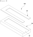
- FIG. 1 is a view schematically showing a device 100 for fabricating a specimen for testing the adhesive force of an electrode active material layer as an embodiment of the present invention
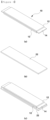
- FIG. 2 is an exploded view showing a device 100 for fabricating a specimen for testing the adhesive force of an electrode active material layer as an embodiment of the present invention
- FIG. 3 is a view schematically showing an embodiment of an electrode 10 and a specimen 20 for testing the adhesive force of an electrode active material layer including the same.
- the device 100 for fabricating a specimen for testing the adhesive force of an electrode active material layer of the present invention is a device used for the fabrication of specimen 20 for testing the adhesive force between the active material layer 12 of the electrode 10 and the current collector 14 (see FIG. 3A ), comprising:
- the active material layer may peel off due to the stress caused by the volume expansion and decrease of the electrode during the charging and discharging process, and there may be a problem that during the process of cutting the electrode, the active material comes off easily even by the momentary pressure at the time of cutting. Therefore, the adhesion state of the active material layer to the current collector plays an important role in the performance of the battery, and thus to confirm this, a test is being conducted to evaluate the adhesive force of the active material layer.
- the measurement of the adhesive force on the current collector of the active material layer is performed by adhering the electrode active material layer to a fixing substrate (e.g., glass substrate) and measuring the adhesive strength while removing the current collector by pulling it in the opposite direction. In this case, if the electrode active material layer of the specimen is not adhered to the correct position of the fixing substrate, accurate measurement results cannot be obtained.
- a fixing substrate e.g., glass substrate
- the adhesive force measurement is performed using a UTM(Universal Testing Machine) device after fabrication of the specimen 20 for testing the adhesive force of the electrode active material layer as shown in (c) of FIG. 3 .
- UTM Universal Testing Machine
- the electrode active material layer 12 is not accurately attached to the position determined by matching the straightness and parallelism to the fixing substrate 22 constituting the specimen 20 for testing the adhesive force of the electrode active material layer, such inaccurate attachment causes a change in the value of the measured tensile force. Therefore, accurate fabrication of the specimen 20 for testing the adhesive force of the electrode active material layer is absolutely required for accurate measurement of the adhesive force on the current collector of the active material layer.
- the device 100 for fabricating a specimen for testing the adhesive force of an electrode active material layer of the present invention provides the effect of easily and conveniently satisfying the conditions required for the specimen as described above. Therefore, according to the present invention, since the generation of incorrectly fabricated specimens is fundamentally prevented, a specimen with an accurate and uniform shape can be fabricated in a simple way, and thus the adhesive force on the current collector of the electrode active material layer can be easily and accurately measured.
- the above coupling means is not particularly limited, and coupling means known in the art may be employed.
- the upper guide panel 40 does not matter what form the upper guide panel 40 is provided in the device 100 for fabricating a specimen for testing the adhesive force of an electrode active material layer as long as it is in a form that can be coupled to the lower guide panel 30 when guiding the electrode active material layer 12.
- the upper guide panel 40 exists in a form separated from the lower guide panel 30, and is provided in a form coupled to the lower guide panel 30 when guiding the electrode active material layer 12; or may be provided in a form in which part or all of it is fixed to the lower guide panel 30.
- the upper guide panel 40 is provided in a form separated from the lower guide panel 30, it may be provided in a detachable structure on the upper surface of the lower guide panel 30 when guiding the electrode active material layer 12.
- a detachable structure structures known in the art may be applied without limitation.
- a coupling fence for detaching the upper guide panel 40 may be provided on the outer circumference of the upper surface of the lower guide panel 30, or conversely, a coupling fence for detaching the lower guide panel 30 may be provided on the outer circumference of the lower surface of the upper guide panel 40.
- a coupling protrusion portion is provided on either the upper guide panel 40 or the lower guide panel 30, and a structure in which a coupling groove portion capable of accommodating the coupling protrusion portion is provided in either the upper guide panel 40 or the lower guide panel 30 is also possible.
- the case of the entirely fixed form is a case that the guide groove 32 of the lower guide panel 30 may be formed in a form into which the fixing substrate 22 can be inserted, even in the state where the upper guide panel 40 is entirely fixed.
- the fixing substrate 22 may be inserted through the open one side wall of the guide groove 32.
- the upper guide panel 40 is fixed to one side of the lower guide panel 30 by a hinge. In this case, while the upper guide panel 40 behaves as shown in FIG. 4 , fabrication of a specimen for testing the adhesive force of the electrode active material layer can be performed.
- the upper guide panel 40 may be coupled in a structure in which the upper guide panel 40 slides in a transverse direction on the upper surface of the lower guide panel 30 slides.
- a guide rail is provided on either the upper guide panel 40 or the lower guide panel 30, and a driving part that slides on the guide rail may be provided in the the other one of the upper guide panel 40 or the lower guide panel 30.
- any one or more of the length or width of the guide hole 42 may be smaller than the corresponding length or width of the guide groove 32.
- the guide groove 32 may be in the form of a square pillar with an open upper surface, and also the guide hole 42 may be in the form of a square pillar with open upper and lower surfaces.
- the guide groove 32 may be in the form of a square pillar with an open upper surface and one side wall
- the guide hole 42 may be in the form of a square pillar with an open upper and lower surface and one side wall.
- one open side wall of the guide groove 32 and one open side wall of the guide hole 42 may be formed in the same direction as shown in FIG. 1 .
- the same direction of the open one side wall may be a longitudinal direction of one side wall of the device for fabricating a specimen for testing the adhesive force of an electrode active material layer.
- the one side wall in the longitudinal direction may be the opposite one side wall to which the hinge is fixed.
- the upper guide panel 40 may be a transparent panel.
- the upper guide panel 40 may be a transparent panel.
- the material of the upper guide panel 40 for example, acrylic resin may be used, but is not limited thereto.
- the upper guide panel 40 may be provided as a transparent panel.
- a material resistant to heat and humidity environment can be preferably used.
- a bakelite material may be used, but is not limited thereto.
- the electrode 10 may have a form in which the current collector 14 and an active material layer 12 are stacked on one or more surfaces of the current collector.
- the electrode 10 may have a form in which active material layers 12 are formed on both sides of the current collector 14 as shown in FIG. 3A .
- the present invention provides a method for fabricating the specimen for testing the adhesive force of the electrode active material layer.
- the method for fabricating the specimen is a method for fabricating a specimen 20 for testing the adhesive force of the electrode active material layer by using the device 100 for fabricating a specimen for testing the adhesive force of an electrode active material layer, which comprises the steps of,
- the present invention may further comprise, after the step (a), a step of coupling the upper guide panel 40 to the upper portion of the lower guide panel 30 so that the guide hole 42 and the guide groove 32 overlap ( FIGS. 4A and 4B ).
- the present invention may further comprise a step of releasing the coupling of the upper guide panel 40 to the upper portion of the lower guide panel 30 before separating the specimen 20 for testing the adhesive force of the electrode active material layer in step (c) above ( FIG. 4E ).
- the adhering when adhering the electrode active material layer 12 in step (b), the adhering may be performed by a method known in the art. For example, it can be implemented by a method of applying an adhesive to the fixing substrate 22 or the active material layer 12 and adhering them, or a method of attaching a double-sided tape to the fixing substrate 22 or the active material layer 12.
- Electrode 12 Active material layer 14: current collector 20: Specimen for testing adhesive force of electrode active material layer 22: Fixing substrate 30: Lower guide panel 32: Guide groove 40: Upper guide panel 42: Guide hole 100: Device for fabricating specimen for testing adhesive force of electrode active material layer
Landscapes
- Chemical & Material Sciences (AREA)
- Immunology (AREA)
- Physics & Mathematics (AREA)
- Health & Medical Sciences (AREA)
- Analytical Chemistry (AREA)
- Biochemistry (AREA)
- General Health & Medical Sciences (AREA)
- Life Sciences & Earth Sciences (AREA)
- General Physics & Mathematics (AREA)
- Pathology (AREA)
- Engineering & Computer Science (AREA)
- Manufacturing & Machinery (AREA)
- Chemical Kinetics & Catalysis (AREA)
- Electrochemistry (AREA)
- General Chemical & Material Sciences (AREA)
- Battery Electrode And Active Subsutance (AREA)
- Sampling And Sample Adjustment (AREA)
Abstract
Description
- The present application claims the benefit of priority based on
Korean Patent Application No. 10-2022-0075353 filed on June 21, 2022 - The present invention relates to a device for fabricating a specimen for testing the adhesive force of an electrode active material layer and a method for fabricating the specimen for testing the adhesive force of the electrode active material layer using the same.
- As the demand for mobile devices, electric vehicles, etc. is increased, the demand for secondary batteries is rapidly increasing. In particular, among secondary batteries, a lithium secondary battery having high energy density and voltage is commercialized and widely used.
- Such a lithium secondary battery has a structure in which an electrode assembly capable of charging and discharging in a positive electrode/separator/negative electrode structure is mounted on a battery case.
- The positive electrode and the negative electrode are manufactured by coating or bonding an active material to a current collector to form an active material layer. For example, they are manufactured by mixing an active material, a binder, and an electrically conductive material in a solvent to prepare a slurry, applying the obtained slurry to the current collector, drying it, and rolling it, or are manufactured by adhering an active material previously prepared in the form of a free-standing film by a dry or wet process to a current collector using an adhesive or the like.
- If the active material layer is not firmly adhered to the current collector, there may be a problem that the active material layer may peel off due to the stress caused by the volume expansion and decrease of the electrode during the charging and discharging process, and the active material comes off easily even by the momentary pressure at the time of cutting during the process of cutting the electrode. Accordingly, the adhesive state of the active material layer to the current collector plays an important role in the performance of the battery, and to confirm this, a test is being conducted to evaluate the adhesive force of the active material layer.
- The measurement of the adhesive force of the active material layer on the current collector is performed by adhering the electrode active material layer to a fixing substrate (e.g., glass substrate) and measuring the adhesive strength while removing the current collector by pulling it in the opposite direction. In this case, if the electrode active material layer of the specimen is not adhered to the correct position of the fixing substrate, accurate measurement results cannot be obtained.
- However, the process of attaching the electrode active material layer of the specimen to the fixing substrate is performed manually, and due to this, it is frequently the case that the active material layer adhered obliquely onto the fixing substrate, resulting in poorly fabricated specimens. In addition, there is a problem even in the accuracy of adhesive force measurement accordingly.
-
Korean Laid-open Utility Model Publication No. 20-2011-0000143 - The present invention was made to solve the above problems of the prior art, and thus it is an object of the present invention to provide a device for fabricating a specimen for testing the adhesive force of an electrode active material layer, which can easily and quickly fabricate a highly reliable specimen by accurately guiding the adhesion position of the active material layer and the fixing substrate when fabricating a specimen for testing the adhesive force of the electrode active material layer.
- In addition, it is another object of the present invention to provide a method for easily and quickly fabricating a specimen for testing the adhesive force of an electrode active material layer, which has high reliability, using the device for fabricating the specimen.
- In order to achieve the above objects, the present invention provides
- a device for fabricating a specimen for testing the adhesive force of the electrode active material layer, which comprises
- a lower guide panel having a guide groove provided on its upper surface wherein the guide groove guides and accommodates a fixing substrate to which the electrode active material layer is adhered; and
- an upper guide panel having a guide hole for guiding the adhesion position of the electrode active material layer to the fixing substrate accommodated in the guide groove,
- wherein at least one of the upper guide panel and the lower guide panel is provided with a coupling means between the upper guide panel and the lower guide panel.
- In one embodiment of the present invention, the upper guide panel exists in a form separated from the lower guide panel, and is provided in a form coupled to the lower guide panel when guiding the electrode active material layer; or may be provided in a form in which part or all of it is fixed to the lower guide panel.
- In one embodiment of the present invention, the upper guide panel may be fixed to one side of the lower guide panel by a hinge.
- In one embodiment of the present invention, the upper guide panel may be coupled in a structure in which it slides in the transverse direction on the upper surface of the lower guide panel, any one of the upper guide panel or the lower guide panel may be provided with a guide rail, and the other one of the upper guide panel or the lower guide panel may be provided with a driving unit that slides on the guide rail.
- In one embodiment of the present invention, in order to hold the fixing substrate accommodated in the guide groove, any one or more of the length or width of the guide hole may be smaller than the corresponding length or width of the guide groove.
- In one embodiment of the present invention, the guide groove may be in the form of a square pillar with an open upper surface or in the form of a square pillar in which the upper surface and one side wall are open.
- In one embodiment of the present invention, the guide hole may be in the form of a square pillar with an open upper or lower surface or in the form of a square pillar with an open upper or lower surface and one side wall.
- In one embodiment of the present invention, one open side wall of the guide groove and the guide hole may be formed in the same direction.
- In one embodiment of the present invention, the upper guide panel may be a transparent panel.
- In addition, the present invention provides
a method for fabricating the specimen for testing the adhesive force of the electrode active material layer, which comprises the steps of: - (a) positioning a fixing substrate in a guide groove provided on a lower guide panel;
- (b) adhering the electrode active material layer to the upper surface of the fixing substrate through a guide hole provided in an upper guide panel; and
- (c) separating the specimen for testing the adhesive force of the electrode active material layer from the device for fabricating the specimen.
- In one embodiment of the present invention, the method may further comprise a step of coupling the upper guide panel to an upper portion of the lower guide panel so that the guide hole and the guide groove overlap after step (a) above.
- In one embodiment of the present invention, the present invention may further comprise a step of releasing the coupling of the upper guide panel to the upper portion of the lower guide panel before separating the specimen for testing the adhesive force of the electrode active material layer in step (c) above.
- In one embodiment of the present invention, the present invention may further comprise a step of attaching the double-sided tape to the fixing substrate or the active material layer upon adhesion of the electrode active material layer in step (b) above.
- The device for fabricating a specimen for testing the adhesive force of an electrode active material layer according to the present invention accurately guides the active material layer and the adhesion position of the fixing substrate during specimen fabrication, thereby enabling reliable specimen fabrication easily and quickly.
- In addition, the method for fabricating the specimen for testing the adhesive force of the electrode active material layer makes it possible to easily and quickly fabricate a highly reliable specimen by using the device for fabricating the specimen.
-
-
FIG. 1 is a view schematically showing a device for fabricating a specimen for testing the adhesive force of an electrode active material layer as an embodiment of the present invention. -
FIG. 2 is an exploded view showing a device for fabricating a specimen for testing the adhesive force of an electrode active material layer as an embodiment of the present invention. -
FIG. 3 is a view schematically showing an embodiment of an electrode and a specimen for testing the adhesive force of an electrode active material layer comprising the same. -
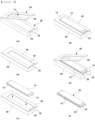
FIG. 4 is a view schematically showing a method for fabricating a specimen for testing the adhesive force of an electrode active material layer as an embodiment of the present invention. -
FIG. 5 is a view schematically showing a method for fabricating a specimen for testing the adhesive force of an electrode active material layer as another embodiment of the present invention. - Hereinafter, embodiments of the present invention will be described in detail with reference to the accompanying drawings so that those skilled in the art can easily carry out the present invention. However, the present invention may be embodied in many different forms and is not limited to the embodiments described herein. The same reference numerals have been assigned to like parts throughout the specification.
- When it is mentioned that a certain component "is connected to, provided with, or installed on" another component, it should be understood that it may be directly connected to or installed on another component, but other components may exist in therebetween. On the other hand, it is mentioned that a certain component is "directly connected to or installed on" another component, it should be understood that there are no other components in the middle. Meanwhile, other expressions describing the relationship between the elements, such as "on the upper portion" and "directly on the upper portion " or "between" and "immediately between" or "neighboring to" and "directly neighboring to", etc., should be interpreted similarly.
-
FIG. 1 is a view schematically showing adevice 100 for fabricating a specimen for testing the adhesive force of an electrode active material layer as an embodiment of the present invention,FIG. 2 is an exploded view showing adevice 100 for fabricating a specimen for testing the adhesive force of an electrode active material layer as an embodiment of the present invention, andFIG. 3 is a view schematically showing an embodiment of anelectrode 10 and aspecimen 20 for testing the adhesive force of an electrode active material layer including the same. Hereinafter, the present invention will be described with reference to the drawings. - The
device 100 for fabricating a specimen for testing the adhesive force of an electrode active material layer of the present invention is a device used for the fabrication ofspecimen 20 for testing the adhesive force between theactive material layer 12 of theelectrode 10 and the current collector 14 (seeFIG. 3A ), comprising: - a
lower guide panel 30 having aguide groove 32 provided on its upper surface wherein the guide groove guides and accommodates afixing substrate 22 to which the electrodeactive material layer 12 is adhered; and - an
upper guide panel 40 having aguide hole 42 for guiding the adhesion position of the electrodeactive material layer 12 to thefixing substrate 22 accommodated in theguide groove 32, - wherein any one or more of the
upper guide panel 40 and thelower guide panel 30 is provided with a coupling means between theupper guide panel 40 and thelower guide panel 30. - In a lithium secondary battery, if the active material layer is not firmly adhered to the current collector, the active material layer may peel off due to the stress caused by the volume expansion and decrease of the electrode during the charging and discharging process, and there may be a problem that during the process of cutting the electrode, the active material comes off easily even by the momentary pressure at the time of cutting. Therefore, the adhesion state of the active material layer to the current collector plays an important role in the performance of the battery, and thus to confirm this, a test is being conducted to evaluate the adhesive force of the active material layer.
- The measurement of the adhesive force on the current collector of the active material layer is performed by adhering the electrode active material layer to a fixing substrate (e.g., glass substrate) and measuring the adhesive strength while removing the current collector by pulling it in the opposite direction. In this case, if the electrode active material layer of the specimen is not adhered to the correct position of the fixing substrate, accurate measurement results cannot be obtained.
- However, the process of attaching the electrode active material layer of the specimen to the fixing substrate is performed manually, and due to this, it is frequently the case that the active material layer adheres obliquely onto the fixing substrate, resulting in poorly fabricated specimens. In addition, there is a problem even in the accuracy of adhesive force measurement accordingly.
- That is, the adhesive force measurement is performed using a UTM(Universal Testing Machine) device after fabrication of the
specimen 20 for testing the adhesive force of the electrode active material layer as shown in (c) ofFIG. 3 . However, if the electrodeactive material layer 12 is not accurately attached to the position determined by matching the straightness and parallelism to the fixingsubstrate 22 constituting thespecimen 20 for testing the adhesive force of the electrode active material layer, such inaccurate attachment causes a change in the value of the measured tensile force. Therefore, accurate fabrication of thespecimen 20 for testing the adhesive force of the electrode active material layer is absolutely required for accurate measurement of the adhesive force on the current collector of the active material layer. - The
device 100 for fabricating a specimen for testing the adhesive force of an electrode active material layer of the present invention provides the effect of easily and conveniently satisfying the conditions required for the specimen as described above. Therefore, according to the present invention, since the generation of incorrectly fabricated specimens is fundamentally prevented, a specimen with an accurate and uniform shape can be fabricated in a simple way, and thus the adhesive force on the current collector of the electrode active material layer can be easily and accurately measured. - The above coupling means is not particularly limited, and coupling means known in the art may be employed.
- In one embodiment of the present invention, it does not matter what form the
upper guide panel 40 is provided in thedevice 100 for fabricating a specimen for testing the adhesive force of an electrode active material layer as long as it is in a form that can be coupled to thelower guide panel 30 when guiding the electrodeactive material layer 12. For example, theupper guide panel 40 exists in a form separated from thelower guide panel 30, and is provided in a form coupled to thelower guide panel 30 when guiding the electrodeactive material layer 12; or may be provided in a form in which part or all of it is fixed to thelower guide panel 30. - If the
upper guide panel 40 is provided in a form separated from thelower guide panel 30, it may be provided in a detachable structure on the upper surface of thelower guide panel 30 when guiding the electrodeactive material layer 12. In this case, as the detachable structure, structures known in the art may be applied without limitation. For example, a coupling fence for detaching theupper guide panel 40 may be provided on the outer circumference of the upper surface of thelower guide panel 30, or conversely, a coupling fence for detaching thelower guide panel 30 may be provided on the outer circumference of the lower surface of theupper guide panel 40. In addition, a coupling protrusion portion is provided on either theupper guide panel 40 or thelower guide panel 30, and a structure in which a coupling groove portion capable of accommodating the coupling protrusion portion is provided in either theupper guide panel 40 or thelower guide panel 30 is also possible. - Among the cases in which the
upper guide panel 40 is partially or entirely fixed to thelower guide panel 30, the case of the entirely fixed form, as shown inFIG. 5 , is a case that theguide groove 32 of thelower guide panel 30 may be formed in a form into which the fixingsubstrate 22 can be inserted, even in the state where theupper guide panel 40 is entirely fixed. For example, when one side wall of theguide groove 32 has an open form, the fixingsubstrate 22 may be inserted through the open one side wall of theguide groove 32. - In addition, in the case of the partially fixed form, for example, as shown in
FIG. 1 , it may be mentioned that theupper guide panel 40 is fixed to one side of thelower guide panel 30 by a hinge. In this case, while theupper guide panel 40 behaves as shown inFIG. 4 , fabrication of a specimen for testing the adhesive force of the electrode active material layer can be performed. - Also, for example, the
upper guide panel 40 may be coupled in a structure in which theupper guide panel 40 slides in a transverse direction on the upper surface of thelower guide panel 30 slides. In this case, a guide rail is provided on either theupper guide panel 40 or thelower guide panel 30, and a driving part that slides on the guide rail may be provided in the the other one of theupper guide panel 40 or thelower guide panel 30. - Among the above structures, considering the fabrication convenience of the specimen for testing the adhesive force of the electrode active material layer, in particular, a form in which the
upper guide panel 40 is fixed to one side of thelower guide panel 30 by a hinge may be preferable. - In one embodiment of the present invention, in order to hold the fixing
substrate 22 accommodated in theguide groove 32, any one or more of the length or width of theguide hole 42 may be smaller than the corresponding length or width of theguide groove 32. - In one embodiment of the present invention, the
guide groove 32 may be in the form of a square pillar with an open upper surface, and also theguide hole 42 may be in the form of a square pillar with open upper and lower surfaces. - In addition, the
guide groove 32 may be in the form of a square pillar with an open upper surface and one side wall, and also theguide hole 42 may be in the form of a square pillar with an open upper and lower surface and one side wall. - Furthermore, one open side wall of the
guide groove 32 and one open side wall of theguide hole 42 may be formed in the same direction as shown inFIG. 1 . In addition, the same direction of the open one side wall may be a longitudinal direction of one side wall of the device for fabricating a specimen for testing the adhesive force of an electrode active material layer. In addition, when theupper guide panel 40 is fixed to one side of thelower guide panel 30 by a hinge, the one side wall in the longitudinal direction may be the opposite one side wall to which the hinge is fixed. - In one embodiment of the present invention, the
upper guide panel 40 may be a transparent panel. When formed as a transparent panel as described above, since the visibility of the fixingsubstrate 22 or the like in the downward direction is improved, it may be preferable. - In one embodiment of the present invention, as the material of the
upper guide panel 40, for example, acrylic resin may be used, but is not limited thereto. In this case, as described above, theupper guide panel 40 may be provided as a transparent panel. - As the material of the
lower guide panel 30, a material resistant to heat and humidity environment can be preferably used. For example, a bakelite material may be used, but is not limited thereto. - In one embodiment of the present invention, the
electrode 10 may have a form in which thecurrent collector 14 and anactive material layer 12 are stacked on one or more surfaces of the current collector. For example, theelectrode 10 may have a form in which active material layers 12 are formed on both sides of thecurrent collector 14 as shown inFIG. 3A . - In addition, the present invention provides a method for fabricating the specimen for testing the adhesive force of the electrode active material layer.
- The method for fabricating the specimen is a method for fabricating a
specimen 20 for testing the adhesive force of the electrode active material layer by using thedevice 100 for fabricating a specimen for testing the adhesive force of an electrode active material layer, which comprises the steps of, - (a) positioning the fixing
substrate 22 on theguide groove 32 provided on the lower guide panel 30 (FIGS. 4A and 4B ); - (b) adhering the electrode
active material layer 12 to the upper surface of the fixingsubstrate 22 through theguide hole 42 provided in the upper guide panel 40 (FIGS. 4C and 4D ); and - (c) separating the
specimen 20 for testing the adhesive force of the electrode active material layer from thedevice 100 for fabricating the specimen 20 (FIGS. 4E and 4F ). - In one embodiment of the present invention, the present invention may further comprise, after the step (a), a step of coupling the
upper guide panel 40 to the upper portion of thelower guide panel 30 so that theguide hole 42 and theguide groove 32 overlap (FIGS. 4A and 4B ). - In one embodiment of the present invention, the present invention may further comprise a step of releasing the coupling of the
upper guide panel 40 to the upper portion of thelower guide panel 30 before separating thespecimen 20 for testing the adhesive force of the electrode active material layer in step (c) above (FIG. 4E ). - In one embodiment of the present invention, when adhering the electrode
active material layer 12 in step (b), the adhering may be performed by a method known in the art. For example, it can be implemented by a method of applying an adhesive to the fixingsubstrate 22 or theactive material layer 12 and adhering them, or a method of attaching a double-sided tape to the fixingsubstrate 22 or theactive material layer 12. - Although the present invention has been described in relation to the above-mentioned preferred embodiments, it is possible to make various modifications and variations without departing from the spirit and scope of the invention. Accordingly, the appended claims will cover these modifications and variations insofar as they fall within the scope of the present invention.
[Description of Symbol] 10: Electrode 12: Active material layer 14: current collector 20: Specimen for testing adhesive force of electrode active material layer 22: Fixing substrate 30: Lower guide panel 32: Guide groove 40: Upper guide panel 42: Guide hole 100: Device for fabricating specimen for testing adhesive force of electrode active material layer
Claims (13)
- A device for fabricating a specimen for testing the adhesive force of an electrode active material layer, the devivce comprising:a lower guide panel having a guide groove provided on its upper surface wherein the guide groove guides and accommodates a fixing substrate to which the electrode active material layer is adhered, andan upper guide panel having a guide hole for guiding an adhesion position of the electrode active material layer to the fixing substrate accommodated in the guide groove,wherein at least one of the upper guide panel and the lower guide panel is provided with a coupling means between the upper guide panel and the lower guide panel.
- The device for fabricating the specimen for testing the adhesive force of the electrode active material layer according to claim 1, wherein the upper guide panel exists in a form separated from the lower guide panel, and is provided in a form coupled to the lower guide panel when guiding the electrode active material layer; or is provided in a form in which part or all of it is fixed to the lower guide panel.
- The device for fabricating the specimen for testing the adhesive force of the electrode active material layer according to claim 2, wherein the upper guide panel is fixed to one side of the lower guide panel by a hinge.
- The device for fabricating the specimen for testing the adhesive force of the electrode active material layer according to claim 2, wherein the upper guide panel is coupled in a structure in which it slides in the transverse direction on the upper surface of the lower guide panel, any one of the upper guide panel or the lower guide panel is provided with a guide rail, and the other one of the upper guide panel or the lower guide panel is provided with a driving unit that slides on the guide rail.
- The device for fabricating the specimen for testing the adhesive force of the electrode active material layer according to claim 1, wherein any one or more of a length or a width of the guide hole is smaller than the corresponding length or width of the guide groove in order to hold the fixing substrate accommodated in the guide groove.
- The device for fabricating the specimen for testing the adhesive force of the electrode active material layer according to claim 1, wherein the guide groove is in a form of a square pillar with an open upper surface or in a form of a square pillar in which the upper surface and one side wall are open.
- The device for fabricating the specimen for testing the adhesive force of the electrode active material layer according to claim 6, wherein the guide hole is in a form of a square pillar with open upper and lower surfaces or in a form of a square pillar with open upper and lower surfaces and one side wall.
- The device for fabricating the specimen for testing the adhesive force of the electrode active material layer according to claim 7, wherein one open side wall of the guide groove and the guide hole are formed in a same direction.
- The device for fabricating the specimen for testing the adhesive force of the electrode active material layer according to claim 1, wherein the upper guide panel is a transparent panel.
- A method for fabricating the specimen for testing the adhesive force of the electrode active material layer by using the device for fabricating the specimen according to claim 1, which comprises the steps of:(a) positioning a fixing substrate in a guide groove provided on a lower guide panel;(b) adhering the electrode active material layer to the upper surface of the fixing substrate through a guide hole provided in an upper guide panel; and(c) separating the specimen for testing the adhesive force of the electrode active material layer from the device for fabricating the specimen.
- The method for fabricating the specimen for testing the adhesive force of the electrode active material layer according to claim 10, further comprising a step of coupling the upper guide panel to an upper portion of the lower guide panel so that the guide hole and the guide groove overlap, after step (a) above.
- The method for fabricating the specimen for testing the adhesive force of the electrode active material layer according to claim 11, further comprising a step of releasing the coupling of the upper guide panel to the upper portion of the lower guide panel before separating the specimen for testing the adhesive force of the electrode active material layer in step (c) above.
- The method for fabricating the specimen for testing the adhesive force of the electrode active material layer according to claim 10, further comprising a step of attaching a double-sided tape to the fixing substrate or the active material layer upon adhesion of the electrode active material layer in step (b) above.
Applications Claiming Priority (2)
| Application Number | Priority Date | Filing Date | Title |
|---|---|---|---|
| KR1020220075353A KR102952949B1 (en) | 2022-06-21 | 2022-06-21 | Specimen making device for electrode active material layer adhesion test and method for producing a specimen for electrode active material layer adhesion test using the same |
| PCT/KR2023/007041 WO2023249269A1 (en) | 2022-06-21 | 2023-05-24 | Device for manufacturing specimen for adhesion test of electrode active material layer and method for manufacturing specimen for adhesion test of electrode active material layer by using same |
Publications (3)
| Publication Number | Publication Date |
|---|---|
| EP4446726A1 true EP4446726A1 (en) | 2024-10-16 |
| EP4446726A4 EP4446726A4 (en) | 2025-07-02 |
| EP4446726B1 EP4446726B1 (en) | 2026-05-20 |
Family
ID=89380158
Family Applications (1)
| Application Number | Title | Priority Date | Filing Date |
|---|---|---|---|
| EP23827389.0A Active EP4446726B1 (en) | 2022-06-21 | 2023-05-24 | METHOD FOR PREPARING A SAMPLE FOR AN ADHESION TEST OF AN ELECTRODEACTIVATED MATERIAL LAYER |
Country Status (6)
| Country | Link |
|---|---|
| US (1) | US20250093256A1 (en) |
| EP (1) | EP4446726B1 (en) |
| JP (1) | JP7701576B2 (en) |
| KR (1) | KR102952949B1 (en) |
| CN (1) | CN118829867A (en) |
| WO (1) | WO2023249269A1 (en) |
Family Cites Families (10)
| Publication number | Priority date | Publication date | Assignee | Title |
|---|---|---|---|---|
| JP2963339B2 (en) * | 1994-05-31 | 1999-10-18 | 東芝電池株式会社 | Battery alignment, assembly method and alignment, assembly equipment |
| US7628066B2 (en) * | 2007-02-22 | 2009-12-08 | Ethicon, Inc. | Apparatus and method for evaluating peel adhesion |
| JP5076834B2 (en) * | 2007-11-22 | 2012-11-21 | トヨタ自動車株式会社 | Cylindrical battery winding device |
| US8043449B1 (en) * | 2009-06-06 | 2011-10-25 | The Boeing Company | Apparatus and method for fabricating shear test coupons |
| KR20110000143U (en) | 2009-06-30 | 2011-01-06 | 주식회사 한진중공업 | Jig for workpiece of shearing test and manufacturing method of the workpiece |
| CN106461533A (en) * | 2014-05-27 | 2017-02-22 | 居间胶带聚合物公司 | Testing device and methods for testing tape seal strength |
| KR20190041852A (en) * | 2017-10-13 | 2019-04-23 | 주식회사 엘지화학 | Guide member, Method of making stacked type battery using the guide member and Stacked type battery manufactured therefrom |
| SE544013C2 (en) * | 2018-06-26 | 2021-11-02 | Powercell Sweden Ab | Membrane electrode assembly, fuel cell stack with membrane electrode as-sembly and alignment tool for fuel cell stack |
| KR102817871B1 (en) * | 2019-06-13 | 2025-06-09 | 삼성전자 주식회사 | Battery stack and method of manufacturing the same |
| FR3101306B1 (en) | 2019-10-01 | 2021-10-15 | Renault Sas | Steering angle control device of a self-driving motor vehicle |
-
2022
- 2022-06-21 KR KR1020220075353A patent/KR102952949B1/en active Active
-
2023
- 2023-05-24 JP JP2024543543A patent/JP7701576B2/en active Active
- 2023-05-24 WO PCT/KR2023/007041 patent/WO2023249269A1/en not_active Ceased
- 2023-05-24 US US18/728,836 patent/US20250093256A1/en active Pending
- 2023-05-24 EP EP23827389.0A patent/EP4446726B1/en active Active
- 2023-05-24 CN CN202380024549.1A patent/CN118829867A/en active Pending
Also Published As
| Publication number | Publication date |
|---|---|
| JP7701576B2 (en) | 2025-07-01 |
| JP2025502489A (en) | 2025-01-24 |
| KR102952949B1 (en) | 2026-04-14 |
| US20250093256A1 (en) | 2025-03-20 |
| EP4446726A4 (en) | 2025-07-02 |
| WO2023249269A1 (en) | 2023-12-28 |
| KR20230174435A (en) | 2023-12-28 |
| EP4446726B1 (en) | 2026-05-20 |
| CN118829867A (en) | 2024-10-22 |
Similar Documents
| Publication | Publication Date | Title |
|---|---|---|
| US20130029212A1 (en) | Insulating Film Attaching Jig and Battery Cell Manufactured by Using the Same | |
| CN111415877B (en) | Manufacturing method and mold of solar cell bonding quality detection standard sample | |
| US10170733B2 (en) | Flexible structure with strain gauge, application to electrochemical lithium-ion batteries in a flexible packaging | |
| US20250093256A1 (en) | Device for fabricating specimen for testing adhesive force of electrode active material layer and method for fabricating specimen for testing adhesive force of electrode active material layer by using same | |
| KR20240044781A (en) | Formation jig of secondary battery and formation method using the same | |
| CN112881927A (en) | Reference electrode assembly, three-electrode half cell and preparation method | |
| CN111426629A (en) | Method and device for testing peeling force between lithium battery binder and foil | |
| KR20160064456A (en) | Method for Adhering of Battery Cell Insulating Tape Using Brushing Member and Automatic Adhesion Machine for the Same | |
| CN114335669B (en) | Cells, Batteries and Electrical Equipment | |
| CN118281284B (en) | Battery coating process | |
| CN113406393B (en) | Device and method for testing volume resistivity of conductive gel | |
| EP4203121A1 (en) | Electrode assembly | |
| KR20080062969A (en) | Fixture for measuring insulation resistance of battery | |
| JP5139647B2 (en) | Method for manufacturing electrode body | |
| CN118060145A (en) | Gluing system and control method | |
| JP7421864B2 (en) | Pressureless bonding process for attaching solar cells to panels | |
| CN212301666U (en) | Positioning jig and battery side voltage testing device | |
| EP4679613A1 (en) | Electrode tab bonding equipment and electrode tab bonding method | |
| US20240175792A1 (en) | Apparatus for Measuring Sealing Strength | |
| US20240068885A1 (en) | Temperature measurement device | |
| US20250023205A1 (en) | Electrochemical device and electrical device | |
| CN219779172U (en) | Batteries, battery packs | |
| CN119447494B (en) | A lithium battery pack method | |
| CN222867964U (en) | Diaphragms, cells, battery packs and electrical equipment | |
| KR20250147452A (en) | Method of measuring adhesiveness for secondary battery |
Legal Events
| Date | Code | Title | Description |
|---|---|---|---|
| STAA | Information on the status of an ep patent application or granted ep patent |
Free format text: STATUS: THE INTERNATIONAL PUBLICATION HAS BEEN MADE |
|
| PUAI | Public reference made under article 153(3) epc to a published international application that has entered the european phase |
Free format text: ORIGINAL CODE: 0009012 |
|
| STAA | Information on the status of an ep patent application or granted ep patent |
Free format text: STATUS: REQUEST FOR EXAMINATION WAS MADE |
|
| 17P | Request for examination filed |
Effective date: 20240710 |
|
| AK | Designated contracting states |
Kind code of ref document: A1 Designated state(s): AL AT BE BG CH CY CZ DE DK EE ES FI FR GB GR HR HU IE IS IT LI LT LU LV MC ME MK MT NL NO PL PT RO RS SE SI SK SM TR |
|
| A4 | Supplementary search report drawn up and despatched |
Effective date: 20250530 |
|
| RIC1 | Information provided on ipc code assigned before grant |
Ipc: H01M 4/04 20060101ALI20250523BHEP Ipc: G01N 19/04 20060101ALI20250523BHEP Ipc: G01N 1/36 20060101AFI20250523BHEP |
|
| DAV | Request for validation of the european patent (deleted) | ||
| DAX | Request for extension of the european patent (deleted) | ||
| GRAP | Despatch of communication of intention to grant a patent |
Free format text: ORIGINAL CODE: EPIDOSNIGR1 |
|
| STAA | Information on the status of an ep patent application or granted ep patent |
Free format text: STATUS: GRANT OF PATENT IS INTENDED |
|
| INTG | Intention to grant announced |
Effective date: 20260305 |
|
| GRAS | Grant fee paid |
Free format text: ORIGINAL CODE: EPIDOSNIGR3 |
|
| GRAA | (expected) grant |
Free format text: ORIGINAL CODE: 0009210 |
|
| STAA | Information on the status of an ep patent application or granted ep patent |
Free format text: STATUS: THE PATENT HAS BEEN GRANTED |