EP4443151A1 - Specimen support, ionization method, and mass spectrometry method - Google Patents
Specimen support, ionization method, and mass spectrometry method Download PDFInfo
- Publication number
- EP4443151A1 EP4443151A1 EP22927247.1A EP22927247A EP4443151A1 EP 4443151 A1 EP4443151 A1 EP 4443151A1 EP 22927247 A EP22927247 A EP 22927247A EP 4443151 A1 EP4443151 A1 EP 4443151A1
- Authority
- EP
- European Patent Office
- Prior art keywords
- sample
- substrate
- porous structure
- protective layer
- sample support
- Prior art date
- Legal status (The legal status is an assumption and is not a legal conclusion. Google has not performed a legal analysis and makes no representation as to the accuracy of the status listed.)
- Withdrawn
Links
Images




Classifications
-
- H—ELECTRICITY
- H01—ELECTRIC ELEMENTS
- H01J—ELECTRIC DISCHARGE TUBES OR DISCHARGE LAMPS
- H01J49/00—Particle spectrometers or separator tubes
- H01J49/02—Details
- H01J49/04—Arrangements for introducing or extracting samples to be analysed, e.g. vacuum locks; Arrangements for external adjustment of electron- or ion-optical components
-
- H—ELECTRICITY
- H01—ELECTRIC ELEMENTS
- H01J—ELECTRIC DISCHARGE TUBES OR DISCHARGE LAMPS
- H01J49/00—Particle spectrometers or separator tubes
- H01J49/02—Details
- H01J49/04—Arrangements for introducing or extracting samples to be analysed, e.g. vacuum locks; Arrangements for external adjustment of electron- or ion-optical components
- H01J49/0409—Sample holders or containers
-
- G—PHYSICS
- G01—MEASURING; TESTING
- G01N—INVESTIGATING OR ANALYSING MATERIALS BY DETERMINING THEIR CHEMICAL OR PHYSICAL PROPERTIES
- G01N27/00—Investigating or analysing materials by the use of electric, electrochemical, or magnetic means
- G01N27/62—Investigating or analysing materials by the use of electric, electrochemical, or magnetic means by investigating the ionisation of gases, e.g. aerosols; by investigating electric discharges, e.g. emission of cathode
-
- G—PHYSICS
- G01—MEASURING; TESTING
- G01N—INVESTIGATING OR ANALYSING MATERIALS BY DETERMINING THEIR CHEMICAL OR PHYSICAL PROPERTIES
- G01N27/00—Investigating or analysing materials by the use of electric, electrochemical, or magnetic means
- G01N27/62—Investigating or analysing materials by the use of electric, electrochemical, or magnetic means by investigating the ionisation of gases, e.g. aerosols; by investigating electric discharges, e.g. emission of cathode
- G01N27/622—Ion mobility spectrometry
- G01N27/623—Ion mobility spectrometry combined with mass spectrometry
-
- H—ELECTRICITY
- H01—ELECTRIC ELEMENTS
- H01J—ELECTRIC DISCHARGE TUBES OR DISCHARGE LAMPS
- H01J49/00—Particle spectrometers or separator tubes
- H01J49/0027—Methods for using particle spectrometers
- H01J49/0031—Step by step routines describing the use of the apparatus
-
- H—ELECTRICITY
- H01—ELECTRIC ELEMENTS
- H01J—ELECTRIC DISCHARGE TUBES OR DISCHARGE LAMPS
- H01J49/00—Particle spectrometers or separator tubes
- H01J49/02—Details
- H01J49/04—Arrangements for introducing or extracting samples to be analysed, e.g. vacuum locks; Arrangements for external adjustment of electron- or ion-optical components
- H01J49/0409—Sample holders or containers
- H01J49/0418—Sample holders or containers for laser desorption, e.g. matrix-assisted laser desorption/ionisation [MALDI] plates or surface enhanced laser desorption/ionisation [SELDI] plates
-
- H—ELECTRICITY
- H01—ELECTRIC ELEMENTS
- H01J—ELECTRIC DISCHARGE TUBES OR DISCHARGE LAMPS
- H01J49/00—Particle spectrometers or separator tubes
- H01J49/02—Details
- H01J49/10—Ion sources; Ion guns
- H01J49/16—Ion sources; Ion guns using surface ionisation, e.g. field-, thermionic- or photo-emission
Definitions
- the present disclosure relates to a sample support, ionization method, and mass spectrometry method.
- a sample support for ionizing a sample such as a biological sample is known (for example, Patent Document 1).
- the sample support has a porous structure formed so as to communicate the first surface and the second surface.
- a conductive layer is provided on the first surface.
- Patent Document 1 WO 2019/155741
- a component of the sample is ionized by irradiating the sample transferred onto the first surface (or the sample sucked up from the second surface side to the first surface side) with an energy beam such as a laser beam.
- an energy beam such as a laser beam.
- noise component background noise
- An object of the present disclosure is to provide a sample support, an ionization method, and a mass spectrometry method capable of effectively suppressing generation of a noise component when a sample is ionized.
- a sample support is a sample support for ionizing a sample, the sample support including a substrate having a first surface, a second surface opposite to the first surface, and a porous structure opening at least to the first surface; a protective layer provided to cover a surface of the porous structure; and a conductive layer provided so as to cover a portion of the protective layer at least provided on the first surface.
- a protective layer is provided so as to cover the surface of the porous structure. That is, the material of the substrate (i.e., particles) is protected by the protective layer so as not to be exposed to the outside. Accordingly, when the sample is ionized by irradiating the first surface of the substrate with the energy beam, it is possible to effectively suppress generation of a component derived from the material of the substrate as a noise component.
- the protective layer may be formed of at least one of an oxide, a fluoride, a nitride, a carbide, and a metal. According to the above-described configuration, the protective layer having the above-described protective function can be suitably formed.
- the protective layer may be formed of at least one of aluminum oxide, magnesium oxide, hafnium oxide, silicon oxide, magnesium fluoride, aluminum nitride, silicon nitride, silicon carbide, tungsten, hafnium, diamond, and graphite. According to the above-described configuration, the protective layer having the above-described protective function can be suitably formed.
- the protective layer may be an ALD layer.
- the protective layer can be densely and continuously formed without a gap on the surface of the porous structure by an atomic layer deposition (ALD) method. According to this, it is possible to suitably suppress the surface of the porous structure from being exposed to the outside, and it is possible to more effectively suppress a component derived from the material of the substrate from being generated as a noise component.
- ALD atomic layer deposition
- the porous structure may be formed of an aggregate of a plurality of particles.
- the porous structure may have a joint in which the particles adjacent to each other are bonded to each other to form a recessed portion between the particles.
- the protective layer may be provided so as to cover at least a portion of surfaces of the plurality of particles and the joint, the portion constituting the first surface. According to the above configuration, the surfaces of the plurality of particles and the joint are protected by the protective layer so as not to be exposed to the outside. This makes it possible to effectively suppress the generation of component derived from the material of the substrate as noise component when ionizing the sample by irradiating the first surface of the substrate with the energy beam, in a case where the porous structure is formed of a plurality of the particles.
- the average diameter of the joint in the porous structure may be equal to or greater than one tenth of the average diameter of the particle in the porous structure and less than the average diameter of the particle. According to the above configuration, the strength of the joint in the porous structure can be ensured, and the strength (rigidity) of the substrate that can withstand the transfer of the sample to the first surface can be ensured.
- the particles may be glass beads. According to the above configuration, a substrate having the above-described porous structure can be suitably obtained at low cost.
- the substrate may be an anodic oxide film formed of valve metals or silicon.
- the porous structure may have a plurality of pores that open at least to the first surface and extend in a thickness direction of the substrate. According to the above-described configuration, in a case where the porous structure is formed of the plurality of pores extending in the thickness direction of the substrate, it is possible to effectively suppress the generation of components derived from the material of the side substrate as noise components when ionizing the sample by irradiating the first surface of the side substrate with the energy beam.
- An ionization method includes a first step of preparing the sample support, a second step of transferring a sample to the first surface, and a third step of ionizing a component of the sample by irradiating the first surface with an energy beam.
- the same effect as that of the above-described sample support can be obtained. That is, when the sample is ionized by irradiating the first surface of the substrate with the energy beam, it is possible to effectively suppress a component derived from the material of the substrate from being generated as a noise component.
- An ionization method includes a first step of preparing a sample support having a porous structure configured to allow a first surface and a second surface to communicate with each other, a second step of placing the sample support on the sample so that the second surface faces the sample, and a third step of ionizing a component of the sample by irradiating the first surface with an energy beam after the component of the sample has moved from the second surface side to the first surface side by a capillary phenomenon.
- the same effect as that of the above-described sample support can be obtained. That is, when the sample is ionized by irradiating the first surface of the substrate with the energy beam, it is possible to effectively suppress a component derived from the material of the substrate from being generated as a noise component.
- a mass spectrometry method includes the first step, the second step, and the third step of the ionization method described above, and a fourth step of detecting the component ionized in the third step.
- the mass spectrometry method by including the first step, the second step, and the third step of the ionization method, the same effects as those of the ionization method are obtained.
- a sample support an ionization method, and a mass spectrometry method capable of effectively suppressing generation of a noise component when a sample is ionized.
- a sample support 1 includes a substrate 2.
- the substrate 2 is formed in a rectangular plate shape.
- the substrate 2 has a first surface 2a and a second surface 2b opposite to the first surface 2a.
- One side of the substrate 2 is, for example, about several centimeters when viewed from a thickness direction of the substrate 2 (that is, the direction in which the first surface 2a and the second surface 2b face each other).
- the thickness of the substrate 2 is, for example, about 100 ⁇ m to 1500 ⁇ m.
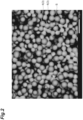
- the substrate 2 is formed with an irregular porous structure 3 opening to the first surface 2a.
- FIG. 2 shows a state before a conductive layer 6 and a protective layer 7 to be described later are formed.
- the irregular porous structure is, for example, a structure in which gaps (fine pores) extend in irregular directions and are irregularly distributed in three dimensions.
- Example of the irregular porous structure includes a structure that enters the substrate 2 from one inlet (opening) on the first surface 2a side and branches into a plurality of paths, and a structure that enters the substrate 2 from a plurality of inlets (openings) on the first surface 2a side and merges into one path.
- a structure in which a plurality of pores extending linearly along the thickness direction of the substrate 2 from the first surface 2a to the second surface 2b are provided as main pores that is, a regular structure constituted by pores extending mainly in one direction
- main pores that is, a regular structure constituted by pores extending mainly in one direction
- the porous structure 3 is formed of, for example, an aggregate of a plurality of bead-like particles.
- the aggregate of a plurality of bead-like particles is a structure in which a plurality of particles are aggregated so as to be in contact with each other.
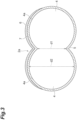
- Examples of the aggregate of a plurality of particles include a structure in which a plurality of particles are adhered or bonded to each other.
- the porous structure 3 is a bead aggregate (aggregate) formed by joining a plurality of spherical beads (particles) to each other. That is, the substrate 2 is formed of the bead aggregate (the porous structure 3) obtained by joining a plurality of beads to each other and forming the beads into a rectangular plate shape.
- the porous structure 3 includes a portion occupied by a plurality of the beads 4 and gaps S between the plurality of the beads 4.
- the beads 4 are glass beads.
- the bead aggregate is, for example, a sintered body of a plurality of glass beads (beads 4).
- the entire of the substrate 2 is made of the porous structure 3.
- the porous structure 3 is formed over the entire region from the first surface 2a to the second surface 2b in the substrate 2.
- the porous structure 3 is formed so as to communicate the first surface 2a and the second surface 2b.
- the substrate 2 has rigidity to the extent that a second step (transfer of a sample Sa (see FIG. 4 )) of the ionizing method described later can be performed. If the substrate 2 is insufficiently rigid, the substrate 2 may be damaged, such as when the sample Sa is pressed against the first surface 2a or when the sample Sa is peeled from the first surface 2a.
- the substrate 2 has rigidity that can withstand the transfer of the sample Sa (that is, the operation of pressing the sample Sa against the first surface 2a and the operation of peeling off the sample Sa from the first surface 2a) (that is, rigidity to the extent that the substrate 2 is not damaged by the transfer of the sample Sa).
- the average diameter of the joints 5 formed between the beads 4 adjacent to each other is equal to or greater than one tenth (1/10) of the average diameter of the beads 4 (the average of the diameter d2 of each beads 4) and less than the average diameter of the beads 4.
- the protective layer 7 is provided so as to cover the surfaces 4a of the porous structure 3 (in the present embodiment, the plurality of beads 4).
- the protective layer 7 is provided so as to cover at least a portion constituting the first surface 2a among the surfaces 4a of the plurality of beads 4 and the joint 5.
- the protective layer 7 is provided so as to cover the entire of the surfaces 4a of the plurality of beads 4 and the joint 5 (the entire surfaces exposed to the outside), including the portion that does not constitute the first surface 2a.
- the protective layer 7 is formed densely and continuously without gaps on the surfaces 4a of the plurality of beads 4 and the joint 5.
- the conductive layer 6 is provided so as to cover a portion of the protective layer 7 at least provided on the first surface 2a.
- the portion of the protective layer 7 provided on the first surface 2a is a portion exposed on the first surface 2a side of the substrate 2.
- the portion is a portion that can be seen when the substrate 2 is viewed from a position facing the first surface 2a.
- the two beads 4 joined to each other are arranged side by side in a direction orthogonal to the thickness direction of the substrate 2, and the upper surfaces of the two beads 4 constitute the first surface 2a. That is, the conductive layer 6 covers the surface of the protective layer 7 exposed on the first surface 2a side so as to straddle the upper surfaces of the two beads 4.
- the conductive layer 6 is formed of a conductive material.
- a conductive material As the material of the conductive layer 6, metals having low affinity (reactivity) with the sample and high conductivity are preferably used for the reasons described below.
- the conductive layer 6 is formed by metals such as Cu having high affinity with samples such as proteins
- the sample is ionized in a state where Cu atom is attached to sample molecules in a process of ionizing the sample to be described later, and a detection result in mass spectrometry to be described later may be deviated by the amount of attachment of the Cu atom. Therefore, metals having a low affinity with the sample are preferably used as the material of the conductive layer 6.
- the higher the conductivity of the metal the easier and more stably a constant voltage can be applied. Therefore, when the conductive layer 6 is formed of metals having high conductivity, a voltage can be uniformly applied to the first surface 2a of the substrate 2. Further, a metal having higher electrical conductivity tends to have higher thermal conductivity. Therefore, when the conductive layer 6 is formed of metals having high conductivity, the energy of an energy beam (for example, a laser beam) applied to the substrate 2 can be efficiently transmitted to the sample through the conductive layer 6. Therefore, metals having high conductivity are preferably used as the material of the conductive layer 6.
- the material of the conductive layer 6 for example, gold, platinum, or the like is preferably used.
- the conductive layer 6 is formed by, for example, a plating method, an atomic layer deposition method (ALD), a vapor deposition method, a sputtering method, or the like so as to have thickness of about 1 nm to 350 nm.
- ALD atomic layer deposition method
- a vapor deposition method a vapor deposition method
- a sputtering method or the like so as to have thickness of about 1 nm to 350 nm.
- Cr chromium
- Ni nickel
- Ti titanium
- the conductive layer 6 is formed so as to cover the surfaces of the protective layer 7 exposed on the first surface 2a side as shown in FIG. 3 , for example, by performing the above-described vapor deposition method, sputtering method, or the like from the first surface 2a side.
- the conductive layer 6 may be formed to cover the entire of the surface of the protective layer 7 covering the surface 4a of each of the beads 4. In this way, the conductive layer 6 may be provided so as to cover not only the portion of the protective layer 7 provided on the first surface 2a but also the entire surface of the protective layer 7.
- the protective layer 7 prevents the beads 4 from being directly irradiated with a laser beam L (a kind of energy beam) when the first surface 2a of the substrate 2 is irradiated with the laser beam L in the third step described later. Accordingly, a component derived from the material of the substrate 2 (that is, the beads 4) is suppressed from being generated as a noise component. That is, the protective layer 7 has a noise reduction function of suppressing the generation of the noise component.
- a laser beam L a kind of energy beam
- the protective layer 7 is preferably formed of a material having a relatively high melting temperature or evaporation start temperature.
- the protective layer 7 may be formed by oxides, fluorides, nitrides, carbides, metals, etc.
- the protective layer 7 may be formed of oxides such as aluminum oxides, magnesium oxides, hafnium oxides, and silicone oxides.
- the protective layer 7 may be formed of fluorides such as magnesium fluorides.
- the protective layer 7 may be formed of nitrides such as aluminum nitrides and silicone nitrides.
- the protective layer 7 may be formed of carbides such as silicone carbides.
- the protective layer 7 may be formed of metals such as tungsten, hafnium, or may be formed of diamond or graphite.
- the protective layer 7 having the above-described protection functions (noise reduction functions) can be suitably formed.
- the protective layer 7 is, for example, not thicker than 100 nm.
- the protective layer 7 may be configured as an ALD layer. That is, the protective layer 7 may be formed by an atomic layer deposition (ALD) method. In this case, as shown in FIG. 3 , the protective layer 7 can be formed densely and continuously without a gap on the surfaces 4a of the plurality of the beads 4 and the joints 5 by ALD. According to this, it is possible to suitably suppress the surface of the beads 4 and the joint 5 from being exposed to the outside, and it is possible to more effectively suppress a component derived from the substrate 2 material (that is, the beads 4) from being generated as a noise component.
- ALD atomic layer deposition
- the method of forming the protective layer 7 is not limited to ALD.
- the protective layer 7 may be formed by a general film forming method such as vapor phase film forming including physical vapor deposition (PVD) such as ion-plating and chemical vapor deposition (CVD), and liquid phase film forming including a sol gel method and coating.
- the protective layer 7 does not necessarily have to be formed so as to cover the surfaces 4a of all of the beads 4 constituting the substrate 2.
- the protective layer 7 may be formed so as to cover the surface 4a of a part of the beads 4 (including the beads 4 constituting the first surface 2a) located on the first surface 2a side of the substrate 2.
- sample support 1 is prepared as a sample support for ionizing a sample (first step).
- the sample support 1 may be prepared by being manufactured by a person who performs the ionizing method and the mass spectrometry method, or may be prepared by being transferred from a manufacturer, a seller, or the like of the sample support 1.
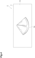
- the sample Sa is transferred to the first surface 2a of the substrate 2 (second step).
- the sample Sa is a slice of a fruit (lemon).
- a component Sa1 of the sample Sa (see FIG. 5 ) is deposited on the first surface 2a by pressing the sample Sa against the first surface 2a of the substrate 2.
- the component Sa1 of the sample Sa adheres to the first surface 2a
- the component Sa1 of the sample Sa is ionized by irradiating the first surface 2a with an energy beam while applying a voltage to the first surface 2a (the conductive layer 6) (third step).
- the above-described third step can be performed by using a mass spectrometer 10 shown in FIG. 5 .
- the mass spectrometer 10 includes a support 12, an irradiation unit 13, a voltage application unit 14, an ion detector 15, a camera 16, a controller 17, and a sample stage 18.
- the sample support 1 is placed on the support 12.
- the support 12 is placed on the sample stage 18.
- the sample support 1 is fixed on a support substrate 8 via a conductive tape 9 in a state where the second surface 2b of the substrate 2 is placed on a support surface 8a of the support substrate 8.
- the support substrate 8 is placed on the support 12.
- the conductive tape 9 is located at the edge of the substrate 2 and extends between the first surface 2a of the substrate 2 and the support surface 8a of the support substrate 8.
- the first surface 2a and the support surface 8a are electrically connected via the conductive tape 9.
- the support substrate 8 may be formed, for example, by a glass slide.
- the support substrate 8 is a glass substrate (ITO slide glass) on which a transparent conductive film such as an indium tin oxide (ITO) film is formed, and the surface of the transparent conductive film is the support surface 8a. That is, in the present embodiment, the entire of the support surface 8a has conductivity.
- ITO indium tin oxide
- the irradiation unit 13 irradiates the first surface 2a of the sample support 1 with energy beam such as the laser beam L.
- the voltage application unit 14 applies a voltage to the first surface 2a of the sample support 1.
- the ion detector 15 detects a component (a sample ion Sa2) of the ionized sample.
- the camera 16 acquires a camera image including an irradiation position of the laser beam L by the irradiation unit 13.
- the camera 16 is, for example, a small CCD camera associated with the irradiation unit 13.
- the controller 17 controls the operation of the sample stage 18, the camera 16, the irradiation unit 13, the voltage application unit 14, and the ion detector 15.
- the controller 17 is, for example, a computer device including a processor (for example, a central processing unit (CPU) or the like), a memory (for example, a read only memory (ROM), a random access memory (RAM), or the like), and the like.
- a processor for example, a central processing unit (CPU) or the like
- a memory for example, a read only memory (ROM), a random access memory (RAM), or the like
- ROM read only memory
- RAM random access memory
- a voltage is applied to the support surface 8a of the support substrate 8 by the voltage application unit 14. As a result, a voltage is applied to the conductive layer 6 (see FIG. 3 ) on the first surface 2a of the substrate 2 via the support surface 8a and the conductive tape 9.
- the controller 17 operates the irradiation unit 13 based on the image acquired by the camera 16. More specifically, the controller 17 operates the irradiation unit 13 so that the laser beam L is irradiated to the first surface 2a in a laser irradiation range (for example, a region in which the component Sa1 of the sample specified based on the image acquired by the camera 16 exists).
- a laser irradiation range for example, a region in which the component Sa1 of the sample specified based on the image acquired by the camera 16 exists.
- the controller 17 moves the sample stage 18 and controls the irradiation operation (irradiation timing and the like) of the laser beam L by the irradiation unit 13. That is, the controller 17 causes the irradiation unit 13 to irradiate the laser beam L after confirming that the sample stage 18 has moved by a predetermined distance. For example, the controller 17 repeats the movement (scanning) of the sample stage 18 and the irradiation of the laser beam L by the irradiation unit 13 so as to raster-scan the laser irradiation range.
- the change of the irradiation position with respect to the first surface 2a may be performed by moving the irradiation unit 13 instead of the sample stage 18 or may be performed by moving both the sample stage 18 and the irradiation unit 13.
- the component Sa1 of the sample on the first surface 2a is ionized, and the sample ion Sa2 is released. More specifically, energy is transmitted from the conductive layer 6 which has absorbed energy of the laser beam L to the component Sa1 of the sample on the first surface 2a, and the component Sa1 which has acquired energy is vaporized and acquires electric charge to become the sample ion Sa2.
- the released sample ion Sa2 moves while accelerating toward ground electrode (not shown) provided between the sample support 1 and the ion detector 15. That is, the sample ion Sa2 moves toward the ground electrode while being accelerated by the potential difference generated between the conductive layer 6 to which the voltage is applied and the ground electrode. Then, the sample ion Sa2 is detected by the ion detector 15 (fourth step).
- the first to third steps described above correspond to an ionizing method using the sample support 1.
- the first to fourth steps described above correspond to a mass spectrometry method using the sample support 1.
- the conductive layer 6 (see FIG. 3 ) is provided so as to cover the surface (that is, the surfaces 4a of the plurality of beads 4) of the porous structure 3 formed of the aggregate of the plurality of bead-like particles (the beads 4 in the present embodiment). That is, the material of the substrate 2 (i.e., the beads 4) is protected by the protective layer 7 so as not to be exposed to the outside.
- the protective layer 7 so as not to be exposed to the outside.
- the same effect as in the above-described effect of the sample support 1 can be obtained. That is, it is possible to effectively suppress generation of a component derived from a material of the substrate 2 as a noise component when a sample is ionized by irradiating the first surface 2a of the substrate 2 with an energy beam.
- the mass spectrometry method using the sample support 1 the same effect as that of the ionizing method can be obtained by including the first step, the second step, and the third step of the ionizing method.
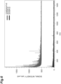
- FIG. 6 is a graph showing the measurement results of blank noise in the Example and the Comparative Example.
- the horizontal axis represents the mass-to-charge ratio (m/z) and the vertical axis represents the signal intensity (arbitrary unit: arb. unit). More specifically, FIG. 6 shows mass spectrum obtained by the above-described mass spectrometry method in a state where there is no sample to be analyzed (that is, a state where the component Sa1 of the sample is not attached to the first surface 2a) for each of the Example and the Comparative Example.
- FIG. 6 shows mass spectrum obtained by the above-described mass spectrometry method in a state where there is no sample to be analyzed (that is, a state where the component Sa1 of the sample is not attached to the first surface 2a) for each of the Example and the Comparative Example.
- the Example is a sample support having a configuration similar to the sample support 1 described above. More particularly, the Example is a sample support having the protective layer 7 (see FIG. 3 ) formed over the surfaces 4a of the beads 4 and the joints 5.
- the protective layer 7 is an ALD film formed by forming a film of aluminum oxide by ALD. Also, the protective layer 7 is 8 nm thick.
- the Comparative Example is a sample support having a configuration in which the protective layer 7 of the sample support 1 described above is omitted. That is, in the Comparative Example, the surfaces 4a of the beads 4 are exposed on the first surface 2a side of the substrate 2.
- the number of types of blank noise (the number of peak signals) in the Example was suppressed to be smaller than the number of types of blank noise in the Comparative Example, and the signal intensity of the blank noise in the Example was smaller than the signal intensity of the blank noise in the Comparative Example.
- the present disclosure is not limited to the embodiments described above.
- the materials and shapes of the components are not limited to the above-described materials and shapes, and various materials and shapes can be used.
- a part of the configuration in one embodiment or modification described above can be arbitrarily applied to the configuration in another embodiment or modification.
- the sample support 1 includes only the substrate 2, but the sample support 1 may include a member other than the substrate 2.
- a support member (a frame or the like) for supporting the substrate 2 may be provided at a part (for example, a corner or the like) of the substrate 2.
- the sample Sa is not limited to the slices of the fruit (lemon) exemplified in the above-described embodiment.
- the sample Sa may have a flat surface, or may have an uneven surface.
- the sample Sa may be other than fruits, and may be, for example, leaves of plants.
- imaging mass spectrometry of the surface (leaf vein) of the leaf can be performed by transferring components of the surface of the leaf, which is the sample Sa, to the first surface 2a.
- the above-described second step may be modified as follows. That is, in the second step, the sample support 1 may be placed on the sample Sa so that the second surface 2b of the substrate 2 faces the sample Sa.
- the sample Sa may be arranged between the support surface 8a of the support substrate 8 and the second surface 2b of the sample support 1.
- the component Sa1 of the sample Sa moves by capillary phenomenon from the second surface 2b side of the substrate 2 through the porous structure 3 (i.e., the gap S) to the first surface 2a side of the substrate 2. That is, in this modified example, in the third step, after the component Sa1 of the sample moves from the second surface 2b side to the first surface 2a side by the capillary phenomenon, the laser beam L may be irradiated to the first surface 2a.
- the same effect as that of the above-described sample support 1 can be obtained in the case of adopting the suction method in which the sample Sa to be ionized is sucked up from the second surface 2b side to the first surface 2a side of the sample support 1 using the capillary phenomenon. That is, it is possible to effectively suppress generation of a component derived from a material of the substrate 2 as a noise component when a sample is ionized by irradiating the first surface 2a of the substrate 2 with an energy beam.
- the entire of the substrate 2 is constituted by the porous structure 3 which is a bead aggregate, but the porous structure 3 may be formed in a part of the substrate 2.
- the porous structure 3 may be formed only in a region of a central portion (a partial region of the first surface 2a) defined as a measurement region for transferring the sample Sa in the substrate 2, and the porous structure 3 may not be formed in other portions of the substrate 2.
- the porous structure 3 may not be formed over the entire region from the first surface 2a to the second surface 2b. That is, the porous structure 3 may be opened at least to the first surface 2a, and may not be opened to the second surface 2b.
- the substrate 2 may be composed of a flat plate and a porous structure provided on the plate.
- the substrate 2 may be constituted by a glass plate and a glass beads aggregate (porous structure) formed of glass beads provided on the glass plate.
- the surface of the glass beads aggregate on the side opposite to the glass plate is the first surface 2a
- the surface of the glass plate on the side opposite to the glass beads aggregate is the second surface 2b.
- the particles constituting the porous structure 3 are not limited to substantially spherical beads, and may have a shape other than a substantially spherical shape.
- the substrate 2 may be an anodic oxide film obtained by anodization of valve metals or silicon.
- valve metal include Al (aluminum), Ta (tantalum), Nb (niobium), Ti (titanium), Hf (hafnium), Zr (zirconium), Zn (zinc), W (tungsten), Bi (bismuth), and Sb (antimony).
- the substrate 2 may be porous alumina obtained by anodic oxidation of aluminum. In this way, the porous structure of the substrate 2 may have a plurality of pores 2c which are open to at least the first surface 2a and extend in the thickness direction of the substrate 2. In other words, as shown in FIGS.
- the porous structure of the substrate 2 may be a structure in which a plurality of pores 2c extending linearly along the thickness direction are provided as main pores (i.e., a regular structure constituted by pores 2c extending mainly in one direction).
- a black portion corresponds to the pore 2c
- a white portion corresponds to the substrate 2 (the partition wall portion between the adjacent pores 2c).
- the protective layer 7 may be provided so as to cover the first surface 2a, the second surface 2b, and inner surfaces of the pores 2c.
- the protective layer 7 may be provided at least on the first surface 2a (i.e., between the conductive layer 6 and the first surface 2a), and is not necessarily provided on the second surface 2b and the inner surfaces of the pores 2c.
- the protective layer 7 is preferably provided not only on the first surface 2a but also on an edge portion of the inner surface of the pore 2c on the first surface 2a side (that is, a part of the inner surface continuous with the first surface 2a).
- the pore 2c is configured as a through hole which penetrates from the first surface 2a to the second surface 2b, but the pore 2c may be a concave hole portion which opens only to the first surface 2a (that is, does not open to the second surface 2b).
- an object to which a voltage is applied by the voltage application unit 14 is not limited to the support surface 8a of the support substrate 8.
- the voltage may be applied to a member (for example, the conductive tape 9) other than the support substrate 8.
- the mass spectrometer 10 may be a scanning-type mass spectrometer or a projection-type mass spectrometer.
- the scan type a signal of one pixel having a size corresponding to the spot size of the laser beam L is acquired for each irradiation of the laser beam L with the irradiation unit 13. That is, scanning (change of irradiation position) and irradiation of the laser beam L are performed for each pixel.
- the projection-type a signal of an image (a plurality of pixels) corresponding to the spot size of the laser beam L is acquired for each irradiation of the laser beam L with the irradiation unit 13.
- imaging mass spectrometry can be performed by irradiating the laser beam L once.
- a signal of the entire sample to be analyzed can be obtained by scanning and irradiating the laser beam L in the same manner as in the scanning-type spectrometer.
- the above-described ionization method can also be used for other measurements and experiments such as ion mobility measurement.
- the use of the sample support 1 is not limited to ionizing samples by irradiation of the laser beam L.
- the sample support 1 can be used for ionizing a sample by irradiation with energy beams such as laser beams, electro-spray, ion beams, and electronic beams.
- energy beams such as laser beams, electro-spray, ion beams, and electronic beams.
- the sample can be ionized by irradiation with such an energy beam.
Landscapes
- Chemical & Material Sciences (AREA)
- Analytical Chemistry (AREA)
- Physics & Mathematics (AREA)
- Health & Medical Sciences (AREA)
- Life Sciences & Earth Sciences (AREA)
- Electrochemistry (AREA)
- Spectroscopy & Molecular Physics (AREA)
- Chemical Kinetics & Catalysis (AREA)
- Biochemistry (AREA)
- General Health & Medical Sciences (AREA)
- General Physics & Mathematics (AREA)
- Immunology (AREA)
- Pathology (AREA)
- Molecular Biology (AREA)
- Optics & Photonics (AREA)
- Engineering & Computer Science (AREA)
- Plasma & Fusion (AREA)
- Other Investigation Or Analysis Of Materials By Electrical Means (AREA)
Abstract
Description
- The present disclosure relates to a sample support, ionization method, and mass spectrometry method.
- A sample support for ionizing a sample such as a biological sample is known (for example, Patent Document 1). The sample support has a porous structure formed so as to communicate the first surface and the second surface. A conductive layer is provided on the first surface.
- Patent Document 1:
WO 2019/155741 - In the sample support as described above, a component of the sample is ionized by irradiating the sample transferred onto the first surface (or the sample sucked up from the second surface side to the first surface side) with an energy beam such as a laser beam. Here, if a component derived from the substrate (porous structure body) is generated as noise component (background noise) when the substrate is irradiated with the laser beam, the detection accuracy of the component of the ionized sample may be reduced.
- An object of the present disclosure is to provide a sample support, an ionization method, and a mass spectrometry method capable of effectively suppressing generation of a noise component when a sample is ionized.
- A sample support according to an aspect of the present disclosure is a sample support for ionizing a sample, the sample support including a substrate having a first surface, a second surface opposite to the first surface, and a porous structure opening at least to the first surface; a protective layer provided to cover a surface of the porous structure; and a conductive layer provided so as to cover a portion of the protective layer at least provided on the first surface.
- In the sample support, a protective layer is provided so as to cover the surface of the porous structure. That is, the material of the substrate (i.e., particles) is protected by the protective layer so as not to be exposed to the outside. Accordingly, when the sample is ionized by irradiating the first surface of the substrate with the energy beam, it is possible to effectively suppress generation of a component derived from the material of the substrate as a noise component.
- The protective layer may be formed of at least one of an oxide, a fluoride, a nitride, a carbide, and a metal. According to the above-described configuration, the protective layer having the above-described protective function can be suitably formed.
- The protective layer may be formed of at least one of aluminum oxide, magnesium oxide, hafnium oxide, silicon oxide, magnesium fluoride, aluminum nitride, silicon nitride, silicon carbide, tungsten, hafnium, diamond, and graphite. According to the above-described configuration, the protective layer having the above-described protective function can be suitably formed.
- The protective layer may be an ALD layer. According to the above-described configuration, the protective layer can be densely and continuously formed without a gap on the surface of the porous structure by an atomic layer deposition (ALD) method. According to this, it is possible to suitably suppress the surface of the porous structure from being exposed to the outside, and it is possible to more effectively suppress a component derived from the material of the substrate from being generated as a noise component.
- The porous structure may be formed of an aggregate of a plurality of particles. The porous structure may have a joint in which the particles adjacent to each other are bonded to each other to form a recessed portion between the particles. The protective layer may be provided so as to cover at least a portion of surfaces of the plurality of particles and the joint, the portion constituting the first surface. According to the above configuration, the surfaces of the plurality of particles and the joint are protected by the protective layer so as not to be exposed to the outside. This makes it possible to effectively suppress the generation of component derived from the material of the substrate as noise component when ionizing the sample by irradiating the first surface of the substrate with the energy beam, in a case where the porous structure is formed of a plurality of the particles.
- The average diameter of the joint in the porous structure may be equal to or greater than one tenth of the average diameter of the particle in the porous structure and less than the average diameter of the particle. According to the above configuration, the strength of the joint in the porous structure can be ensured, and the strength (rigidity) of the substrate that can withstand the transfer of the sample to the first surface can be ensured.
- The particles may be glass beads. According to the above configuration, a substrate having the above-described porous structure can be suitably obtained at low cost.
- The substrate may be an anodic oxide film formed of valve metals or silicon. The porous structure may have a plurality of pores that open at least to the first surface and extend in a thickness direction of the substrate. According to the above-described configuration, in a case where the porous structure is formed of the plurality of pores extending in the thickness direction of the substrate, it is possible to effectively suppress the generation of components derived from the material of the side substrate as noise components when ionizing the sample by irradiating the first surface of the side substrate with the energy beam.
- An ionization method according to another aspect of the present disclosure includes a first step of preparing the sample support, a second step of transferring a sample to the first surface, and a third step of ionizing a component of the sample by irradiating the first surface with an energy beam.
- According to the above-described ionization method, in the case of adopting the transfer method in which the sample to be ionized is transferred to the first surface of the above-described sample support, the same effect as that of the above-described sample support can be obtained. That is, when the sample is ionized by irradiating the first surface of the substrate with the energy beam, it is possible to effectively suppress a component derived from the material of the substrate from being generated as a noise component.
- An ionization method according to another aspect of the present disclosure includes a first step of preparing a sample support having a porous structure configured to allow a first surface and a second surface to communicate with each other, a second step of placing the sample support on the sample so that the second surface faces the sample, and a third step of ionizing a component of the sample by irradiating the first surface with an energy beam after the component of the sample has moved from the second surface side to the first surface side by a capillary phenomenon.
- According to the above-described ionization method, in the case of adopting the suction method in which the sample to be ionized is sucked up from the second surface side to the first surface side of the above-described sample support by using the capillary phenomenon, the same effect as that of the above-described sample support can be obtained. That is, when the sample is ionized by irradiating the first surface of the substrate with the energy beam, it is possible to effectively suppress a component derived from the material of the substrate from being generated as a noise component.
- A mass spectrometry method according to another aspect of the present disclosure includes the first step, the second step, and the third step of the ionization method described above, and a fourth step of detecting the component ionized in the third step.
- According to the mass spectrometry method, by including the first step, the second step, and the third step of the ionization method, the same effects as those of the ionization method are obtained.
- According to the present disclosure, it is possible to provide a sample support, an ionization method, and a mass spectrometry method capable of effectively suppressing generation of a noise component when a sample is ionized.
-
-
FIG. 1 is a perspective view of a sample support according to an embodiment. -
FIG. 2 is an enlarged image of a region A shown inFIG. 1 . -
FIG. 3 is a diagram schematically showing a state of a bead aggregate constituting the first surface. -
FIG. 4 is a view showing a second step in the mass spectrometry method of one embodiment. -
FIG. 5 is a configuration diagram of a mass spectrometer in which the mass spectrometry method of the embodiment is performed. -
FIG. 6 is a graph showing the measurement results of blank noise in the example and the comparative example. -
FIG. 7 is an enlarged image of a portion corresponding to a region A of a substrate according to a modification. -
FIG. 8 is a diagram schematically showing a cross-sectional structure of a part of the substrate according to the modification. - Hereinafter, embodiments of the present invention will be described in detail with reference to the drawings. In the drawings, the same or corresponding parts are denoted by the same reference numerals, and redundant description will be omitted. In the drawings, some characteristic parts according to the embodiment are exaggerated for easy understanding. Therefore, the dimensional ratios in the drawings may be different from the actual dimensional ratios.
- As shown in
FIG. 1 , asample support 1 includes asubstrate 2. As an example, thesubstrate 2 is formed in a rectangular plate shape. Thesubstrate 2 has afirst surface 2a and asecond surface 2b opposite to thefirst surface 2a. One side of thesubstrate 2 is, for example, about several centimeters when viewed from a thickness direction of the substrate 2 (that is, the direction in which thefirst surface 2a and thesecond surface 2b face each other). The thickness of the substrate 2 (distance from thefirst surface 2a to thesecond surface 2b) is, for example, about 100 µm to 1500 µm. - As shown in
FIG. 2 , thesubstrate 2 is formed with an irregularporous structure 3 opening to thefirst surface 2a.FIG. 2 shows a state before aconductive layer 6 and aprotective layer 7 to be described later are formed. The irregular porous structure is, for example, a structure in which gaps (fine pores) extend in irregular directions and are irregularly distributed in three dimensions. Example of the irregular porous structure includes a structure that enters thesubstrate 2 from one inlet (opening) on thefirst surface 2a side and branches into a plurality of paths, and a structure that enters thesubstrate 2 from a plurality of inlets (openings) on thefirst surface 2a side and merges into one path. On the other hand, for example, a structure in which a plurality of pores extending linearly along the thickness direction of thesubstrate 2 from thefirst surface 2a to thesecond surface 2b are provided as main pores (that is, a regular structure constituted by pores extending mainly in one direction) is not included in the irregular porous structure. - The
porous structure 3 is formed of, for example, an aggregate of a plurality of bead-like particles. The aggregate of a plurality of bead-like particles is a structure in which a plurality of particles are aggregated so as to be in contact with each other. Examples of the aggregate of a plurality of particles include a structure in which a plurality of particles are adhered or bonded to each other. In the present embodiment, theporous structure 3 is a bead aggregate (aggregate) formed by joining a plurality of spherical beads (particles) to each other. That is, thesubstrate 2 is formed of the bead aggregate (the porous structure 3) obtained by joining a plurality of beads to each other and forming the beads into a rectangular plate shape. Theporous structure 3 includes a portion occupied by a plurality of thebeads 4 and gaps S between the plurality of thebeads 4. - In the present embodiment, the
beads 4 are glass beads. In this case, the bead aggregate is, for example, a sintered body of a plurality of glass beads (beads 4). According to the above configuration, by using the glass beads, it is possible to suitably and inexpensively obtain thesubstrate 2 having the irregularporous structure 3. In the present embodiment, the entire of thesubstrate 2 is made of theporous structure 3. In other words, theporous structure 3 is formed over the entire region from thefirst surface 2a to thesecond surface 2b in thesubstrate 2. Thus, theporous structure 3 is formed so as to communicate thefirst surface 2a and thesecond surface 2b. - As shown in
FIG. 3 , thebeads 4 adjacent to each other are joined (fused) to each other. A recessed portion is formed between thebeads 4 by joining thebeads 4 adjacent to each other. That is, theporous structure 3 has a joint 5 that forms the recessed portion. Here, thesubstrate 2 has rigidity to the extent that a second step (transfer of a sample Sa (seeFIG. 4 )) of the ionizing method described later can be performed. If thesubstrate 2 is insufficiently rigid, thesubstrate 2 may be damaged, such as when the sample Sa is pressed against thefirst surface 2a or when the sample Sa is peeled from thefirst surface 2a. Therefore, thesubstrate 2 has rigidity that can withstand the transfer of the sample Sa (that is, the operation of pressing the sample Sa against thefirst surface 2a and the operation of peeling off the sample Sa from thefirst surface 2a) (that is, rigidity to the extent that thesubstrate 2 is not damaged by the transfer of the sample Sa). In the present embodiment, the average diameter of thejoints 5 formed between thebeads 4 adjacent to each other (the average of the diameter dl of each joint 5) is equal to or greater than one tenth (1/10) of the average diameter of the beads 4 (the average of the diameter d2 of each beads 4) and less than the average diameter of thebeads 4. According to the above-described configuration, it is possible to ensure the strength of the joint 5 in theporous structure 3, and it is possible to ensure the substrate strength (rigidity) that can withstand the transfer of the sample Sa to thefirst surface 2a. - Further, as shown in
FIG. 3 , theprotective layer 7 is provided so as to cover thesurfaces 4a of the porous structure 3 (in the present embodiment, the plurality of beads 4). Theprotective layer 7 is provided so as to cover at least a portion constituting thefirst surface 2a among thesurfaces 4a of the plurality ofbeads 4 and thejoint 5. In the present embodiment, as an example, theprotective layer 7 is provided so as to cover the entire of thesurfaces 4a of the plurality ofbeads 4 and the joint 5 (the entire surfaces exposed to the outside), including the portion that does not constitute thefirst surface 2a. For example, theprotective layer 7 is formed densely and continuously without gaps on thesurfaces 4a of the plurality ofbeads 4 and thejoint 5. Theconductive layer 6 is provided so as to cover a portion of theprotective layer 7 at least provided on thefirst surface 2a. Here, the portion of theprotective layer 7 provided on thefirst surface 2a is a portion exposed on thefirst surface 2a side of thesubstrate 2. For example, the portion is a portion that can be seen when thesubstrate 2 is viewed from a position facing thefirst surface 2a. In the example ofFIG. 3 , the twobeads 4 joined to each other are arranged side by side in a direction orthogonal to the thickness direction of thesubstrate 2, and the upper surfaces of the twobeads 4 constitute thefirst surface 2a. That is, theconductive layer 6 covers the surface of theprotective layer 7 exposed on thefirst surface 2a side so as to straddle the upper surfaces of the twobeads 4. - The
conductive layer 6 is formed of a conductive material. As the material of theconductive layer 6, metals having low affinity (reactivity) with the sample and high conductivity are preferably used for the reasons described below. - For example, when the
conductive layer 6 is formed by metals such as Cu having high affinity with samples such as proteins, the sample is ionized in a state where Cu atom is attached to sample molecules in a process of ionizing the sample to be described later, and a detection result in mass spectrometry to be described later may be deviated by the amount of attachment of the Cu atom. Therefore, metals having a low affinity with the sample are preferably used as the material of theconductive layer 6. - On the other hand, the higher the conductivity of the metal, the easier and more stably a constant voltage can be applied. Therefore, when the
conductive layer 6 is formed of metals having high conductivity, a voltage can be uniformly applied to thefirst surface 2a of thesubstrate 2. Further, a metal having higher electrical conductivity tends to have higher thermal conductivity. Therefore, when theconductive layer 6 is formed of metals having high conductivity, the energy of an energy beam (for example, a laser beam) applied to thesubstrate 2 can be efficiently transmitted to the sample through theconductive layer 6. Therefore, metals having high conductivity are preferably used as the material of theconductive layer 6. - From the above viewpoint, as the material of the
conductive layer 6, for example, gold, platinum, or the like is preferably used. Theconductive layer 6 is formed by, for example, a plating method, an atomic layer deposition method (ALD), a vapor deposition method, a sputtering method, or the like so as to have thickness of about 1 nm to 350 nm. As the material of theconductive layer 6, for example, Cr (chromium), Ni (nickel), Ti (titanium), or the like may be used. - The
conductive layer 6 is formed so as to cover the surfaces of theprotective layer 7 exposed on thefirst surface 2a side as shown inFIG. 3 , for example, by performing the above-described vapor deposition method, sputtering method, or the like from thefirst surface 2a side. On the other hand, when theconductive layer 6 is formed by ALD, theconductive layer 6 may be formed to cover the entire of the surface of theprotective layer 7 covering thesurface 4a of each of thebeads 4. In this way, theconductive layer 6 may be provided so as to cover not only the portion of theprotective layer 7 provided on thefirst surface 2a but also the entire surface of theprotective layer 7. - The
protective layer 7 prevents thebeads 4 from being directly irradiated with a laser beam L (a kind of energy beam) when thefirst surface 2a of thesubstrate 2 is irradiated with the laser beam L in the third step described later. Accordingly, a component derived from the material of the substrate 2 (that is, the beads 4) is suppressed from being generated as a noise component. That is, theprotective layer 7 has a noise reduction function of suppressing the generation of the noise component. - From the viewpoint of effectively exhibiting the noise reduction function, the
protective layer 7 is preferably formed of a material having a relatively high melting temperature or evaporation start temperature. For example, theprotective layer 7 may be formed by oxides, fluorides, nitrides, carbides, metals, etc. In addition, theprotective layer 7 may be formed of oxides such as aluminum oxides, magnesium oxides, hafnium oxides, and silicone oxides. Theprotective layer 7 may be formed of fluorides such as magnesium fluorides. Theprotective layer 7 may be formed of nitrides such as aluminum nitrides and silicone nitrides. Theprotective layer 7 may be formed of carbides such as silicone carbides. Alternatively, theprotective layer 7 may be formed of metals such as tungsten, hafnium, or may be formed of diamond or graphite. When theprotective layer 7 is formed of the above-described material, theprotective layer 7 having the above-described protection functions (noise reduction functions) can be suitably formed. Theprotective layer 7 is, for example, not thicker than 100 nm. - The
protective layer 7 may be configured as an ALD layer. That is, theprotective layer 7 may be formed by an atomic layer deposition (ALD) method. In this case, as shown inFIG. 3 , theprotective layer 7 can be formed densely and continuously without a gap on thesurfaces 4a of the plurality of thebeads 4 and thejoints 5 by ALD. According to this, it is possible to suitably suppress the surface of thebeads 4 and the joint 5 from being exposed to the outside, and it is possible to more effectively suppress a component derived from thesubstrate 2 material (that is, the beads 4) from being generated as a noise component. - However, the method of forming the
protective layer 7 is not limited to ALD. For example, theprotective layer 7 may be formed by a general film forming method such as vapor phase film forming including physical vapor deposition (PVD) such as ion-plating and chemical vapor deposition (CVD), and liquid phase film forming including a sol gel method and coating. In addition, theprotective layer 7 does not necessarily have to be formed so as to cover thesurfaces 4a of all of thebeads 4 constituting thesubstrate 2. For example, theprotective layer 7 may be formed so as to cover thesurface 4a of a part of the beads 4 (including thebeads 4 constituting thefirst surface 2a) located on thefirst surface 2a side of thesubstrate 2. - An example of an ionizing method and a mass spectrometry method using the
sample support 1 will be described. First, the above-describedsample support 1 is prepared as a sample support for ionizing a sample (first step). Thesample support 1 may be prepared by being manufactured by a person who performs the ionizing method and the mass spectrometry method, or may be prepared by being transferred from a manufacturer, a seller, or the like of thesample support 1. - Subsequently, as shown in
FIG. 4 , the sample Sa is transferred to thefirst surface 2a of the substrate 2 (second step). In the example ofFIG. 4 , the sample Sa is a slice of a fruit (lemon). For example, a component Sa1 of the sample Sa (seeFIG. 5 ) is deposited on thefirst surface 2a by pressing the sample Sa against thefirst surface 2a of thesubstrate 2. - Subsequently, after the component Sa1 of the sample Sa adheres to the
first surface 2a, the component Sa1 of the sample Sa is ionized by irradiating thefirst surface 2a with an energy beam while applying a voltage to thefirst surface 2a (the conductive layer 6) (third step). As an example, the above-described third step can be performed by using amass spectrometer 10 shown inFIG. 5 . Themass spectrometer 10 includes asupport 12, anirradiation unit 13, avoltage application unit 14, anion detector 15, acamera 16, acontroller 17, and asample stage 18. - The
sample support 1 is placed on thesupport 12. Thesupport 12 is placed on thesample stage 18. Here, as an example, thesample support 1 is fixed on asupport substrate 8 via aconductive tape 9 in a state where thesecond surface 2b of thesubstrate 2 is placed on asupport surface 8a of thesupport substrate 8. With thesample support 1 thus fixed on thesupport substrate 8, thesupport substrate 8 is placed on thesupport 12. Theconductive tape 9 is located at the edge of thesubstrate 2 and extends between thefirst surface 2a of thesubstrate 2 and thesupport surface 8a of thesupport substrate 8. Thefirst surface 2a and thesupport surface 8a are electrically connected via theconductive tape 9. Thesupport substrate 8 may be formed, for example, by a glass slide. In the present embodiment, as an example, thesupport substrate 8 is a glass substrate (ITO slide glass) on which a transparent conductive film such as an indium tin oxide (ITO) film is formed, and the surface of the transparent conductive film is thesupport surface 8a. That is, in the present embodiment, the entire of thesupport surface 8a has conductivity. - The
irradiation unit 13 irradiates thefirst surface 2a of thesample support 1 with energy beam such as the laser beam L. Thevoltage application unit 14 applies a voltage to thefirst surface 2a of thesample support 1. Theion detector 15 detects a component (a sample ion Sa2) of the ionized sample. Thecamera 16 acquires a camera image including an irradiation position of the laser beam L by theirradiation unit 13. Thecamera 16 is, for example, a small CCD camera associated with theirradiation unit 13. Thecontroller 17 controls the operation of thesample stage 18, thecamera 16, theirradiation unit 13, thevoltage application unit 14, and theion detector 15. Thecontroller 17 is, for example, a computer device including a processor (for example, a central processing unit (CPU) or the like), a memory (for example, a read only memory (ROM), a random access memory (RAM), or the like), and the like. - A voltage is applied to the
support surface 8a of thesupport substrate 8 by thevoltage application unit 14. As a result, a voltage is applied to the conductive layer 6 (seeFIG. 3 ) on thefirst surface 2a of thesubstrate 2 via thesupport surface 8a and theconductive tape 9. - Subsequently, the
controller 17 operates theirradiation unit 13 based on the image acquired by thecamera 16. More specifically, thecontroller 17 operates theirradiation unit 13 so that the laser beam L is irradiated to thefirst surface 2a in a laser irradiation range (for example, a region in which the component Sa1 of the sample specified based on the image acquired by thecamera 16 exists). - As an example, the
controller 17 moves thesample stage 18 and controls the irradiation operation (irradiation timing and the like) of the laser beam L by theirradiation unit 13. That is, thecontroller 17 causes theirradiation unit 13 to irradiate the laser beam L after confirming that thesample stage 18 has moved by a predetermined distance. For example, thecontroller 17 repeats the movement (scanning) of thesample stage 18 and the irradiation of the laser beam L by theirradiation unit 13 so as to raster-scan the laser irradiation range. The change of the irradiation position with respect to thefirst surface 2a may be performed by moving theirradiation unit 13 instead of thesample stage 18 or may be performed by moving both thesample stage 18 and theirradiation unit 13. - By the above-described third step, the component Sa1 of the sample on the
first surface 2a is ionized, and the sample ion Sa2 is released. More specifically, energy is transmitted from theconductive layer 6 which has absorbed energy of the laser beam L to the component Sa1 of the sample on thefirst surface 2a, and the component Sa1 which has acquired energy is vaporized and acquires electric charge to become the sample ion Sa2. The released sample ion Sa2 moves while accelerating toward ground electrode (not shown) provided between thesample support 1 and theion detector 15. That is, the sample ion Sa2 moves toward the ground electrode while being accelerated by the potential difference generated between theconductive layer 6 to which the voltage is applied and the ground electrode. Then, the sample ion Sa2 is detected by the ion detector 15 (fourth step). - The first to third steps described above correspond to an ionizing method using the
sample support 1. In addition, the first to fourth steps described above correspond to a mass spectrometry method using thesample support 1. - In the above-described the
sample support 1, the conductive layer 6 (seeFIG. 3 ) is provided so as to cover the surface (that is, thesurfaces 4a of the plurality of beads 4) of theporous structure 3 formed of the aggregate of the plurality of bead-like particles (thebeads 4 in the present embodiment). That is, the material of the substrate 2 (i.e., the beads 4) is protected by theprotective layer 7 so as not to be exposed to the outside. Thus, when the sample is ionized by irradiating thefirst surface 2a of thesubstrate 2 with the energy beam (that is, the third step described above), it is possible to effectively suppress the generation of a component derived from the material of thesubstrate 2 as a noise component. In addition, in the above-described configuration, since theconductive layer 6 is not covered with theprotective layer 7 and is exposed to the outside, it is possible to easily and reliably apply a voltage to theconductive layer 6, compared to a case where theconductive layer 6 is covered with theprotective layer 7. - The
porous structure 3 is formed of an aggregate of a plurality of bead-like particles (beads 4 in the present embodiment). Theporous structure 3 has a joint 5 in which thebeads 4 adjacent to each other are bonded to each other to form a recessed portion between theparticles 4. Theprotective layer 7 is provided so as to cover at least a portion constituting thefirst surface 2a among thesurfaces 4a of the plurality ofbeads 4 and the joint5 (in the present embodiment, the entire of thesurfaces 4a of the plurality ofbeads 4 and the joint 5). According to the above-described configuration, thesurfaces 4a of the plurality ofbeads 4 and the joint 5 are protected by theprotective layer 7 so as not to be exposed to the outside. This makes it possible to effectively suppress the generation of component derived from the material of thesubstrate 2 as noise component when ionizing a sample by irradiating thefirst surface 2a of thesubstrate 2 with an energy beam, in a case where theporous structure 3 is formed of a plurality of thebeads 4. - In addition, according to the ionizing method using the sample support 1 (the first step to the third step), in a case where a transfer method in which the sample Sa to be ionized is transferred to the
first surface 2a of thesample support 1 is performed, the same effect as in the above-described effect of thesample support 1 can be obtained. That is, it is possible to effectively suppress generation of a component derived from a material of thesubstrate 2 as a noise component when a sample is ionized by irradiating thefirst surface 2a of thesubstrate 2 with an energy beam. In addition, according to the mass spectrometry method using the sample support 1 (the first step to the fourth step), the same effect as that of the ionizing method can be obtained by including the first step, the second step, and the third step of the ionizing method. -
FIG. 6 is a graph showing the measurement results of blank noise in the Example and the Comparative Example. InFIG. 6 , the horizontal axis represents the mass-to-charge ratio (m/z) and the vertical axis represents the signal intensity (arbitrary unit: arb. unit). More specifically,FIG. 6 shows mass spectrum obtained by the above-described mass spectrometry method in a state where there is no sample to be analyzed (that is, a state where the component Sa1 of the sample is not attached to thefirst surface 2a) for each of the Example and the Comparative Example. InFIG. 6 , in order to facilitate comparison between the mass spectrum of the Example and the mass spectrum of the Comparative Example, the origin of the signal intensity of the mass spectrum of the Comparative example (that is, a value corresponding to a signal intensity of 0) is shifted by "+ 500". - The Example is a sample support having a configuration similar to the
sample support 1 described above. More particularly, the Example is a sample support having the protective layer 7 (seeFIG. 3 ) formed over thesurfaces 4a of thebeads 4 and thejoints 5. In the Example, theprotective layer 7 is an ALD film formed by forming a film of aluminum oxide by ALD. Also, theprotective layer 7 is 8 nm thick. - The Comparative Example is a sample support having a configuration in which the
protective layer 7 of thesample support 1 described above is omitted. That is, in the Comparative Example, thesurfaces 4a of thebeads 4 are exposed on thefirst surface 2a side of thesubstrate 2. - As shown in
FIG. 6 , in the Comparative Example, significant blank noise (i.e., background noise detected in the absence of a sample) was detected particularly in the low-mass region (60 m/z to 400 m/z). If the sample to be analyzed has a peak signal in the low-mass region, the presence of the blank noise may make it difficult to detect (analyze) the peak signal. - On the other hand, in the Example in which the above-described
protective layer 7 was formed, although some blank noise was detected in the above-described low-mass region, it was confirmed that the occurrence of blank noise was significantly suppressed compared to the Comparative Example. That is, it was confirmed that the blank noise derived from thebeads 4 was reduced by covering at least a portion constituting thefirst surface 2a among thesurfaces 4a of thebeads 4 and thejoints 5 with theprotective layer 7 in thefirst surface 2a irradiated with the energy beam ( the laser beam L). More specifically, it was confirmed that the number of types of blank noise (the number of peak signals) in the Example was suppressed to be smaller than the number of types of blank noise in the Comparative Example, and the signal intensity of the blank noise in the Example was smaller than the signal intensity of the blank noise in the Comparative Example. - The present disclosure is not limited to the embodiments described above. The materials and shapes of the components are not limited to the above-described materials and shapes, and various materials and shapes can be used. In addition, a part of the configuration in one embodiment or modification described above can be arbitrarily applied to the configuration in another embodiment or modification.
- For example, in the above-described embodiment, the
sample support 1 includes only thesubstrate 2, but thesample support 1 may include a member other than thesubstrate 2. For example, a support member (a frame or the like) for supporting thesubstrate 2 may be provided at a part (for example, a corner or the like) of thesubstrate 2. - The sample Sa is not limited to the slices of the fruit (lemon) exemplified in the above-described embodiment. The sample Sa may have a flat surface, or may have an uneven surface. The sample Sa may be other than fruits, and may be, for example, leaves of plants. In this case, imaging mass spectrometry of the surface (leaf vein) of the leaf can be performed by transferring components of the surface of the leaf, which is the sample Sa, to the
first surface 2a. - In addition, as in the above-described embodiment, in a case where the entire of the
substrate 2 is made of theporous structure 3, that is, in a case where thesample support 1 has theporous structure 3 configured to communicate thefirst surface 2a and thesecond surface 2b, the above-described second step may be modified as follows. That is, in the second step, thesample support 1 may be placed on the sample Sa so that thesecond surface 2b of thesubstrate 2 faces the sample Sa. For example, in the above-described embodiment, the sample Sa may be arranged between thesupport surface 8a of thesupport substrate 8 and thesecond surface 2b of thesample support 1. In this case, the component Sa1 of the sample Sa moves by capillary phenomenon from thesecond surface 2b side of thesubstrate 2 through the porous structure 3 (i.e., the gap S) to thefirst surface 2a side of thesubstrate 2. That is, in this modified example, in the third step, after the component Sa1 of the sample moves from thesecond surface 2b side to thefirst surface 2a side by the capillary phenomenon, the laser beam L may be irradiated to thefirst surface 2a. According to the ionizing method and the mass spectrometry method including the second step and the third step according to the above-described modification, the same effect as that of the above-describedsample support 1 can be obtained in the case of adopting the suction method in which the sample Sa to be ionized is sucked up from thesecond surface 2b side to thefirst surface 2a side of thesample support 1 using the capillary phenomenon. That is, it is possible to effectively suppress generation of a component derived from a material of thesubstrate 2 as a noise component when a sample is ionized by irradiating thefirst surface 2a of thesubstrate 2 with an energy beam. - Further, in the above-described embodiment, the entire of the
substrate 2 is constituted by theporous structure 3 which is a bead aggregate, but theporous structure 3 may be formed in a part of thesubstrate 2. For example, theporous structure 3 may be formed only in a region of a central portion (a partial region of thefirst surface 2a) defined as a measurement region for transferring the sample Sa in thesubstrate 2, and theporous structure 3 may not be formed in other portions of thesubstrate 2. Further, theporous structure 3 may not be formed over the entire region from thefirst surface 2a to thesecond surface 2b. That is, theporous structure 3 may be opened at least to thefirst surface 2a, and may not be opened to thesecond surface 2b. For example, thesubstrate 2 may be composed of a flat plate and a porous structure provided on the plate. As an example, thesubstrate 2 may be constituted by a glass plate and a glass beads aggregate (porous structure) formed of glass beads provided on the glass plate. In this case, the surface of the glass beads aggregate on the side opposite to the glass plate is thefirst surface 2a, and the surface of the glass plate on the side opposite to the glass beads aggregate is thesecond surface 2b. - The particles constituting the
porous structure 3 are not limited to substantially spherical beads, and may have a shape other than a substantially spherical shape. - Further, the
substrate 2 may be an anodic oxide film obtained by anodization of valve metals or silicon. Examples of the valve metal include Al (aluminum), Ta (tantalum), Nb (niobium), Ti (titanium), Hf (hafnium), Zr (zirconium), Zn (zinc), W (tungsten), Bi (bismuth), and Sb (antimony). For example, thesubstrate 2 may be porous alumina obtained by anodic oxidation of aluminum. In this way, the porous structure of thesubstrate 2 may have a plurality ofpores 2c which are open to at least thefirst surface 2a and extend in the thickness direction of thesubstrate 2. In other words, as shown inFIGS. 7 and8 , the porous structure of thesubstrate 2 may be a structure in which a plurality ofpores 2c extending linearly along the thickness direction are provided as main pores (i.e., a regular structure constituted bypores 2c extending mainly in one direction). InFIG. 7 , a black portion corresponds to thepore 2c, and a white portion corresponds to the substrate 2 (the partition wall portion between theadjacent pores 2c). - In this case, as shown in
FIG. 8 , theprotective layer 7 may be provided so as to cover thefirst surface 2a, thesecond surface 2b, and inner surfaces of thepores 2c. Theprotective layer 7 may be provided at least on thefirst surface 2a (i.e., between theconductive layer 6 and thefirst surface 2a), and is not necessarily provided on thesecond surface 2b and the inner surfaces of thepores 2c. However, from the viewpoint of suitably suppressing the generation of noise component derived from the material of thesubstrate 2 when thefirst surface 2a is irradiated with the laser light L, theprotective layer 7 is preferably provided not only on thefirst surface 2a but also on an edge portion of the inner surface of thepore 2c on thefirst surface 2a side (that is, a part of the inner surface continuous with thefirst surface 2a). According to the above-described configuration, in the case where the porous structure is formed by the plurality ofpores 2c extending in the thickness direction of thesubstrate 2, it is possible to effectively suppress the generation of component derived from the material of thesubstrate 2 as noise component when ionizing the sample by irradiating thefirst surface 2a of thesubstrate 2 with the energy beam. In the example ofFIG. 8 , thepore 2c is configured as a through hole which penetrates from thefirst surface 2a to thesecond surface 2b, but thepore 2c may be a concave hole portion which opens only to thefirst surface 2a (that is, does not open to thesecond surface 2b). - Further, in the mass spectrometry method using the
sample support 1, an object to which a voltage is applied by thevoltage application unit 14 is not limited to thesupport surface 8a of thesupport substrate 8. For example, the voltage may be applied to a member (for example, the conductive tape 9) other than thesupport substrate 8. - In the mass spectrometry method using the
sample support 1, themass spectrometer 10 may be a scanning-type mass spectrometer or a projection-type mass spectrometer. In the case of the scan type, a signal of one pixel having a size corresponding to the spot size of the laser beam L is acquired for each irradiation of the laser beam L with theirradiation unit 13. That is, scanning (change of irradiation position) and irradiation of the laser beam L are performed for each pixel. On the other hand, in the case of the projection-type, a signal of an image (a plurality of pixels) corresponding to the spot size of the laser beam L is acquired for each irradiation of the laser beam L with theirradiation unit 13. In the case of the projection-type spectrometer, when the entire sample to be analyzed is included in the spot size of the laser beam L, imaging mass spectrometry can be performed by irradiating the laser beam L once. When the entire sample to be analyzed is not included in the spot size of the laser beam L in the projection-type spectrometer, a signal of the entire sample to be analyzed can be obtained by scanning and irradiating the laser beam L in the same manner as in the scanning-type spectrometer. The above-described ionization method can also be used for other measurements and experiments such as ion mobility measurement. - The use of the
sample support 1 is not limited to ionizing samples by irradiation of the laser beam L. Thesample support 1 can be used for ionizing a sample by irradiation with energy beams such as laser beams, electro-spray, ion beams, and electronic beams. In the ionization method and the mass spectrometry method described above, the sample can be ionized by irradiation with such an energy beam. - 1: sample support, 2: substrate, 2a: first surface, 2b: second surface, 2c: pore, 3: porous structure, 4: beads (particle), 4a: surface, 5: joint, 6: conductive layer, 7: protective layer, L: laser beam (energy beam), Sa: sample, Sa1: component, Sa2: sample ion.
Claims (11)
- A sample support for ionizing a sample, comprising:a substrate having a first surface, a second surface opposite to the first surface, and a porous structure opening at least to the first surface;a protective layer provided to cover a surface of the porous structure; anda conductive layer provided so as to cover a portion of the protective layer at least provided on the first surface.
- The sample support according to claim 1, wherein the protective layer is formed of at least one of an oxide, a fluoride, a nitride, a carbide, and a metal.
- The sample support according to claim 1, wherein the protective layer is formed of at least one of aluminum oxide, magnesium oxide, hafnium oxide, silicon oxide, magnesium fluoride, aluminum nitride, silicon nitride, silicon carbide, tungsten, hafnium, diamond, and graphite.
- The sample support according to any one of claims 1 to 3, wherein the protective layer is an ALD layer.
- The sample support according to any one of claims 1 to 4, whereinthe porous structure is formed of an aggregate of a plurality of particles,the porous structure has a joint in which the particles adjacent to each other are bonded to each other to form a recessed portion between the particles, andthe protective layer is provided so as to cover at least a portion of surfaces of the plurality of particles and the joint, the portion constituting the first surface.
- The sample support according to claim 5, wherein an average diameter of the joint in the porous structure is equal to or greater than one tenth of an average diameter of the particle in the porous structure and less than the average diameter of the particle.
- The sample support according to claim 5 or 6, wherein the particles are glass beads.
- The sample support according to any one of claims 1 to 5, whreinthe substrate is an anodic oxide film formed of valve metals or silicon, andthe porous structure has a plurality of pores that open at least to the first surface and extend in a thickness direction of the substrate.
- An ionization method including:a first step of preparing the sample support according to claim 1;a second step of transferring the sample to the first surface; anda third step of ionizing a component of the sample by irradiating the first surface with an energy beam.
- An ionization method including:a first step of preparing the sample support according to claim 1, the sample support having the porous structure configured to allow the first surface and the second surface to communicate with each other;a second step of placing the sample support on the sample so that the second surface faces the sample; anda third step of ionizing the component of the sample by irradiating the first surface with an energy beam after the component of the sample has moved from the second surface side to the first surface side by a capillary phenomenon.
- A mass spectrometry method including:the first step, the second step, and the third step of the ionization method according to claim 9 or 10; anda fourth step of detecting the component ionized in the third step.
Applications Claiming Priority (2)
| Application Number | Priority Date | Filing Date | Title |
|---|---|---|---|
| JP2022021999A JP2023119236A (en) | 2022-02-16 | 2022-02-16 | Sample support, ionization method, and mass spectrometry method |
| PCT/JP2022/033329 WO2023157353A1 (en) | 2022-02-16 | 2022-09-05 | Specimen support, ionization method, and mass spectrometry method |
Publications (1)
| Publication Number | Publication Date |
|---|---|
| EP4443151A1 true EP4443151A1 (en) | 2024-10-09 |
Family
ID=87577859
Family Applications (1)
| Application Number | Title | Priority Date | Filing Date |
|---|---|---|---|
| EP22927247.1A Withdrawn EP4443151A1 (en) | 2022-02-16 | 2022-09-05 | Specimen support, ionization method, and mass spectrometry method |
Country Status (5)
| Country | Link |
|---|---|
| US (1) | US20250095977A1 (en) |
| EP (1) | EP4443151A1 (en) |
| JP (1) | JP2023119236A (en) |
| CN (1) | CN118696229A (en) |
| WO (1) | WO2023157353A1 (en) |
Families Citing this family (2)
| Publication number | Priority date | Publication date | Assignee | Title |
|---|---|---|---|---|
| JP7492065B1 (en) | 2023-06-07 | 2024-05-28 | 浜松ホトニクス株式会社 | Sample support and method for producing the same |
| JP7589320B1 (en) | 2023-11-29 | 2024-11-25 | 浜松ホトニクス株式会社 | Sample Support |
Family Cites Families (3)
| Publication number | Priority date | Publication date | Assignee | Title |
|---|---|---|---|---|
| US20060024713A1 (en) * | 2004-06-30 | 2006-02-02 | Butler John H | Synthesis of oligomers in arrays |
| WO2019155741A1 (en) * | 2018-02-09 | 2019-08-15 | 浜松ホトニクス株式会社 | Sample support |
| JP7333280B2 (en) * | 2020-02-04 | 2023-08-24 | 浜松ホトニクス株式会社 | SAMPLE SUPPORT AND METHOD FOR MANUFACTURING SAMPLE SUPPORT |
-
2022
- 2022-02-16 JP JP2022021999A patent/JP2023119236A/en active Pending
- 2022-09-05 EP EP22927247.1A patent/EP4443151A1/en not_active Withdrawn
- 2022-09-05 WO PCT/JP2022/033329 patent/WO2023157353A1/en not_active Ceased
- 2022-09-05 CN CN202280091833.6A patent/CN118696229A/en active Pending
- 2022-09-05 US US18/728,112 patent/US20250095977A1/en active Pending
Also Published As
| Publication number | Publication date |
|---|---|
| CN118696229A (en) | 2024-09-24 |
| WO2023157353A1 (en) | 2023-08-24 |
| US20250095977A1 (en) | 2025-03-20 |
| JP2023119236A (en) | 2023-08-28 |
Similar Documents
| Publication | Publication Date | Title |
|---|---|---|
| US20250095977A1 (en) | Specimen support, ionization method, and mass spectrometry method | |
| CN111094966B (en) | Sample support | |
| EP3832300B1 (en) | Sample support, sample ionization method, and mass spectrometry method | |
| EP3686590B1 (en) | Laser desorption/ionization method and mass spectrometry method | |
| EP3751266A1 (en) | Sample support | |
| EP3751272A1 (en) | Sample support, ionization method, and mass spectrometry method | |
| EP4102219A1 (en) | Specimen carrier and method for manufacturing specimen carrier | |
| EP4443150A1 (en) | Specimen support, ionization method, and mass spectrometry method | |
| CN111512150B (en) | Sample support, method for producing sample support, and method for ionizing sample | |
| US10971345B2 (en) | Mass spectrometer and mass spectrometry method | |
| EP3751271B1 (en) | Sample support, ionization method, and mass spectrometry method | |
| US20220223396A1 (en) | Sample support, adapter, ionization method and mass spectrometry method | |
| EP4407309A1 (en) | Sample support body and method for manufacturing sample support body | |
| EP3686589B1 (en) | Laser desorption/ionization method and mass spectrometry method | |
| EP3943927A1 (en) | Sample support, ionization method, and mass spectrometry method | |
| EP3751275A1 (en) | Sample support, ionization method, and mass spectrometry method | |
| WO2021100271A1 (en) | Sample support | |
| EP4407653A1 (en) | Support unit, support body, and ionization method | |
| US20210033564A1 (en) | Sample support body and production method for sample support body | |
| EP4116694A1 (en) | Sample support, ionization method, and mass spectrometry method | |
| EP4116695A1 (en) | Sample support, ionization method, and mass spectrometry method | |
| EP4685476A1 (en) | Sample support and method for manufacturing sample support | |
| EP4685475A1 (en) | Sample support and method for manufacturing sample support |
Legal Events
| Date | Code | Title | Description |
|---|---|---|---|
| STAA | Information on the status of an ep patent application or granted ep patent |
Free format text: STATUS: THE INTERNATIONAL PUBLICATION HAS BEEN MADE |
|
| PUAI | Public reference made under article 153(3) epc to a published international application that has entered the european phase |
Free format text: ORIGINAL CODE: 0009012 |
|
| STAA | Information on the status of an ep patent application or granted ep patent |
Free format text: STATUS: REQUEST FOR EXAMINATION WAS MADE |
|
| 17P | Request for examination filed |
Effective date: 20240703 |
|
| AK | Designated contracting states |
Kind code of ref document: A1 Designated state(s): AL AT BE BG CH CY CZ DE DK EE ES FI FR GB GR HR HU IE IS IT LI LT LU LV MC MK MT NL NO PL PT RO RS SE SI SK SM TR |
|
| DAV | Request for validation of the european patent (deleted) | ||
| DAX | Request for extension of the european patent (deleted) | ||
| STAA | Information on the status of an ep patent application or granted ep patent |
Free format text: STATUS: THE APPLICATION HAS BEEN WITHDRAWN |
|
| 18W | Application withdrawn |
Effective date: 20250919 |