EP4440054A1 - Encoding differential signals for power and noise reduction - Google Patents
Encoding differential signals for power and noise reduction Download PDFInfo
- Publication number
- EP4440054A1 EP4440054A1 EP23217621.4A EP23217621A EP4440054A1 EP 4440054 A1 EP4440054 A1 EP 4440054A1 EP 23217621 A EP23217621 A EP 23217621A EP 4440054 A1 EP4440054 A1 EP 4440054A1
- Authority
- EP
- European Patent Office
- Prior art keywords
- encoding scheme
- encoding
- quantifying
- net positive
- differential
- Prior art date
- Legal status (The legal status is an assumption and is not a legal conclusion. Google has not performed a legal analysis and makes no representation as to the accuracy of the status listed.)
- Pending
Links
Images



Classifications
-
- H—ELECTRICITY
- H04—ELECTRIC COMMUNICATION TECHNIQUE
- H04L—TRANSMISSION OF DIGITAL INFORMATION, e.g. TELEGRAPHIC COMMUNICATION
- H04L25/00—Baseband systems
- H04L25/02—Details ; arrangements for supplying electrical power along data transmission lines
- H04L25/0264—Arrangements for coupling to transmission lines
- H04L25/0272—Arrangements for coupling to multiple lines, e.g. for differential transmission
-
- G—PHYSICS
- G06—COMPUTING OR CALCULATING; COUNTING
- G06F—ELECTRIC DIGITAL DATA PROCESSING
- G06F1/00—Details not covered by groups G06F3/00 - G06F13/00 and G06F21/00
- G06F1/26—Power supply means, e.g. regulation thereof
- G06F1/32—Means for saving power
- G06F1/3203—Power management, i.e. event-based initiation of a power-saving mode
- G06F1/3206—Monitoring of events, devices or parameters that trigger a change in power modality
- G06F1/3215—Monitoring of peripheral devices
-
- H—ELECTRICITY
- H03—ELECTRONIC CIRCUITRY
- H03M—CODING; DECODING; CODE CONVERSION IN GENERAL
- H03M5/00—Conversion of the form of the representation of individual digits
- H03M5/02—Conversion to or from representation by pulses
-
- G—PHYSICS
- G06—COMPUTING OR CALCULATING; COUNTING
- G06F—ELECTRIC DIGITAL DATA PROCESSING
- G06F1/00—Details not covered by groups G06F3/00 - G06F13/00 and G06F21/00
- G06F1/26—Power supply means, e.g. regulation thereof
- G06F1/32—Means for saving power
- G06F1/3203—Power management, i.e. event-based initiation of a power-saving mode
- G06F1/3234—Power saving characterised by the action undertaken
- G06F1/324—Power saving characterised by the action undertaken by lowering clock frequency
-
- H—ELECTRICITY
- H03—ELECTRONIC CIRCUITRY
- H03K—PULSE TECHNIQUE
- H03K19/00—Logic circuits, i.e. having at least two inputs acting on one output; Inverting circuits
- H03K19/0008—Arrangements for reducing power consumption
-
- H—ELECTRICITY
- H03—ELECTRONIC CIRCUITRY
- H03K—PULSE TECHNIQUE
- H03K19/00—Logic circuits, i.e. having at least two inputs acting on one output; Inverting circuits
- H03K19/0175—Coupling arrangements; Interface arrangements
- H03K19/017509—Interface arrangements
-
- H—ELECTRICITY
- H04—ELECTRIC COMMUNICATION TECHNIQUE
- H04L—TRANSMISSION OF DIGITAL INFORMATION, e.g. TELEGRAPHIC COMMUNICATION
- H04L25/00—Baseband systems
- H04L25/38—Synchronous or start-stop systems, e.g. for Baudot code
- H04L25/40—Transmitting circuits; Receiving circuits
- H04L25/49—Transmitting circuits; Receiving circuits using code conversion at the transmitter; using predistortion; using insertion of idle bits for obtaining a desired frequency spectrum; using three or more amplitude levels ; Baseband coding techniques specific to data transmission systems
- H04L25/4906—Transmitting circuits; Receiving circuits using code conversion at the transmitter; using predistortion; using insertion of idle bits for obtaining a desired frequency spectrum; using three or more amplitude levels ; Baseband coding techniques specific to data transmission systems using binary codes
Definitions
- Embodiments pertain to circuitry that reduce power consumption and noise in a differential input/output (I/O) buffer.
- I/O input/output
- FIG. 1 illustrates, by way of example, voltage diagrams that help explain operation of a DBI power reduction technique.
- a decision to invert one or more bits is made.
- One or more bits are inverted if the number of transitions with highest power consumption (Setting S 01 , S 10 transitions from low to high) is greater than the number of transitions with zero power consumption (Sets S 00 or S 11 ).
- a DBI signal Scode
- RX Receiver device
- the encoded data is then inverted again (decoded) based on the DBI signal (Scode) to obtain the original data.
- Pulse Amplitude Modulation 4-level (PAM4) is used as the differential signal application. Other differential I/O applications can be addressed similarly.
- Table 1 provides a description of PAM4 voltage and transition power levels. TABLE 1: normalized power for PAM4 data transitions Signal Trans. P Trans. P Power N Trans.
- Table 1 shows signal data and voltage transitions for one differential signal pair (positive side (P) of the differential lines and negative side (N) of the differential lines) for PAM4.
- the voltage levels and associated data are one possible representative set, as there is no governing industrial standard.
- Table 1 shows normalized power consumed with each associated data transition. Note that Table 1 could be augmented to further include noise for each transition as well.
- the power for P and N signal lines is determined as follows: no voltage change ⁇ 0 power consumed; decrease in voltage ⁇ 0 power consumed; increase in voltage ⁇ positive power consumed; and an amount of power consumed with voltage increases in proportion to increase in voltage.
- the representative numbers chosen for the normalized power consumed are 0, 1, 2, 3. Actual normalized power consumption depends on specific transmit and receive circuitry and channel characteristics.
- the power consumed in transitions on P and N lines are added together to give the total power for the differential pair (sometimes called a "lane"). As expected, some data transitions consume higher power than others. There are sixteen possible transitions for each lane. These sixteen possibilities are sorted in decreasing order of power consumed in Table 1. Thus, the first two rows, where either the P or N line has a voltage increase of 500 mV, have the highest power consumption of all. The last four rows have zero power since the voltage level does not change.
- each lane of the I/O bus undergoes one of sixteen transitions listed in Table 1.
- a power aware scheme can thus include:
- Equations 1 and 2 and the power aware scheme can be adjusted to account for noise as well.
- the power consumed can be weighted and the noise component can be weighted as well.
- the weights can indicate the relative importance for the noise and power in the overall power reduction and noise reduction scheme. If power is more important, then a higher weight can be used for the power than the noise and vice versa.
- the logic to determine the encoding scheme to implement in encoding the data can consider both the weighted noise and the weighted power.
- a simpler scheme for encoding/decoding involves bit inversions, similar to DBI for single ended signal buses.
- this can take four forms: no bits inverted, 1 st bit inversion, 2 nd bit inversion, or inversion of both bits.
- 1 st bit is assumed to be the P bit and the 2 nd bit is assumed to be the N bit.
- Table 2 shows how each of the sixteen possible transitions get modified with bit inversions.
- Table 2 also shows a corresponding change in normalized power consumption.
- the positive power saved values indicate power reduction while negative values indicate power increased when applying the scheme. Summing up the power change for each scheme yields zero. This indicates that for a random distribution of data transitions the average power change is zero using any one of the schemes (if applied unconditionally).
- the chosen scheme should be selective.
- the chosen scheme should be used for best power savings given the specific set of transitions at each clock edge.
- Table 2 Inversion schemes. B0* and B1* indicate data values at the previous clock edge, B0 and B1 indicate the data values to be transmitted at the next clock edge; B0 & B1 may be inverted using the inversion scheme or without any inversion.
- ⁇ P k is the change in power for each transition k and N k is the number of signal pairs undergoing transition k at the given clock edge.
- Equation 3 For the three schemes of Table 2, equations (4)-(6) below are sufficient to ensure a reduction in power consumption. These suboptimal conditions can be implemented with combinatorial logic alone and do not require computations for the generic condition of Equation 3.
- Table 3 Logic to Determine when bit inversion will provide power benefit.
- X 2 B 0 & ⁇ B 0 ⁇ & ⁇ B 1 OR ⁇ B 0 & B 0 ⁇ & ⁇ B 1 OR ⁇ B 0 & ⁇ B 0 ⁇ & B 1 & ⁇ B 1 ⁇ OR ⁇ B 0 & ⁇ B 0 ⁇ & ⁇ B 1 & B 1 ⁇ OR B 0 & B 0 ⁇ & B 1
- the different bit inversion schemes offer benefits for different sets of data transitions. Thus, it is possible to get further savings by combining the schemes.
- the code transmitted to the receiver would be more than one bit to indicate which coding scheme is implemented. For example, code “00” indicating no coding, "01” indicating 1 st bit inversion, "10” indicating 2 nd bit inversion, and "11” indicating inversion of both bits.
- Another class of encoding/decoding schemes for power reduction includes performing a predetermined swapping of transitions.
- This table then can be used as a lookup table on the transmit and receive for encoding and decoding.
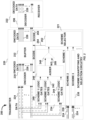
- FIG. 2 illustrates, by way of example, a diagram of an embodiment of a system 200 that includes improved data management. Since different encoding schemes offer benefits for different sets of data transitions, further savings are possible by combining the schemes.
- the system 200 in FIG. 2 provides for the possibility of using different encoding schemes on data.
- the code (“Scode") that indicates the encoding scheme is transmitted to the receive device.
- the Scode in such examples is more than one bit to indicate which coding scheme is implemented. For example, code "00" indicating no coding, "01” indicating 1 st bit inversion, "10” indicating 2 nd bit inversion, and "11” indicating inversion of both bits.
- the system 200 as illustrated includes a transmitter220 and a receiver222.
- the transmitter 220 encodes data 224, received in the form of differential signals, and transmits the data in encoded form as encoded data 226.
- the receiver 222 receives the encoded data 226.
- the receiver 222 decodes the encoded data 226 to recover decoded data 228.
- the decoded data 228 equals the data 224 from the transmitter 220.
- the transmitter 220 includes an encoder 230 and data buffers 232 (differential signal buffer).
- the transmitter 220 includes encoding scheme quantifying and selection circuitry 221.
- the encoding scheme quantifying and selection circuitry 221 includes scheme quantifying logic 234, 236, 238 and a scheme selector 252, sometimes called "scheme selection circuitry".
- the respective scheme quantifying logic 234, 236, 238 provides a value indicating a benefit provided from using a respective encoding scheme on the data 224.
- the encoding schemes discussed thus far are (i) no encoding, (ii) 1 st bit inversion, (iii) 2 nd bit inversion, (iv) both bit inversion, and (v) swap table encoding.
- Each scheme quantifying logic 234, 236, 238 includes logic gates (e.g., AND, OR, XOR, negate, buffer, or the like) that are configured to determine whether a given bit pair of the data 224 will benefit from the encoding scheme.
- the quantifying logic 234, 236, 238 can further determine a number of the lanes of the data 224 that will benefit from the encoding scheme. The number can be an integer greater than, or equal to, zero.
- the logic gates 240, 242, 244 can detect whether a given lane of the data 224 will benefit from encoding using a 1 st bit inversion, the logic gates 240, 242, 244 will benefit from encoding using a 2 nd bit inversion, or the logic gates 240, 242, 244 will benefit from encoding by inverting both bits.
- the quantifying logic 234 can thus detect whether the data 224 will benefit from a type of bit inversion, swapping, or other encoding scheme.
- the quantifying logic 234 can further provide a value that indicates an amount that the data 224 will benefit from the given bit inversion scheme. A higher integer value can indicate more benefit from the inversion scheme.
- the scheme selector 252 receives output from the quantifying logic 234, 236, 238 (the value to the scheme selector 252 that indicates whether the encoding scheme has a net benefit on the data 224, a value indicating an amount of benefit the encoding scheme has on the data 224, or a combination thereof).
- the scheme selector 252 selects an encoding scheme that has a net power benefit on the data 224.
- the scheme selector 252 can select the first scheme, in a hierarchy of schemes, that has a benefit on the data 224, the scheme that has the highest benefit on the data 224, or can select the scheme based on some other heuristic.
- the scheme selector 252 generates an scode 254 that indicates which encoding scheme to use to encode the data 224.
- the encoder 230 receives the scode 254 and encodes the data 224 based on the scheme indicated by the scode 254. An output of the encoder 230 is encoded data 226. Encoded data 226 is the data 224 altered in accord with the encoding scheme indicated by the scode 254.
- the buffer 232 is an electronic circuit element used to isolate the encoded data 226 from the receive device 222.
- the buffer 232 receives the encoded data 226 and the scode 254.
- the buffer 232 provides the encoded data 226 and the scode 254 to the receive device 222.
- the input impedance of the buffer 232 is relatively high compared to the impedance of the receive device 222.
- the buffer 232 draws very little current so as to avoid disturbing the encoded data 226.
- the buffer 232 is sometimes called a unity gain buffer, because it does not intentionally amplify or attenuate the input signal.
- the receive device 222 includes a decoder 256 that reverses the encoding performed by the encoder 230.
- the decoder 256 uses the scode 254 to identify the encoding scheme implemented by the encoder 230. Then the decoder 256 decodes the data based on the encoding scheme indicated by the scode 254.
- An output of the decoder 256 is decoded data 228 that should be identical to the encoded data 226 (in terms of digital code, but may be at a different voltage level than the encoded data 226).
- the decoded data 228 is then provided to a destination electronic component, such as a memory, processing unit, multiplexer, register, or the like.
- One or more of the encoder 230, buffer 232, decoder 256, scheme quantifying logic 234, 236, 238, scheme selector 252, or a component thereof can be implemented using electric or electronic components.
- the electric or electronic components can include one or more transistors, resistors, capacitors, diodes, amplifiers, inductors, multiplexers, logic gates (e.g., AND, OR, XOR, negate, buffer, a combination thereof, or the like), power supplies, oscillators, switches, processing units (e.g., central processing units (CPUs), application specific integrated circuits (ASICs), field programmable gate arrays (FPGAs), graphics processing units (GPUs), or the like), analog to digital converters, digital to analog converters, transducers, transformers, buck or boost converters, a combination thereof, or the like.
- CPUs central processing units
- ASICs application specific integrated circuits
- FPGAs field programmable gate arrays
- GPUs graphics processing units
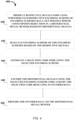
- FIG. 4 illustrates, by way of example, a diagram of an embodiment of a method 400 for power consumption reduction in an I/O buffer using a selectable encoding scheme.
- the method 400 as illustrated includes producing (e.g., by encoding scheme quantifying circuitry 234) respective signals indicating whether each respective encoding scheme of encoding schemes has a net positive power consumption reduction in a differential signal buffer based on differential signals, at operation 440; selecting (e.g., by encoding scheme selection circuitry 252) an encoding scheme of the encoding schemes based on the respective signals, at operation 442; generating (by the encoding scheme selection circuitry 252) a selection code 254 indicating the selected encoding scheme, at operation 444; encoding (e.g., by an encoder 230) the differential signals using the selected encoding scheme indicated by the selection code 254 resulting in encoded data 226, at operation 446; and providing the encoded data 226 to the differential signal buffer 232, at operation 448.
- the encoding schemes can include two or more of inverting only a first bit of each differential signal of the differential signals, inverting only a second bit of each differential signal of the differential signals, inverting both bits of each differential signal of the differential signals, or swapping the bits of each differential signal of the differential signals in accord with a table.
- the method 400 can further include determining (e.g., by the encoding scheme quantifying circuitry 234) an amount to which each of the encoding schemes provides the net positive power reduction.
- the method 400 can further include selecting (e.g., by the encoding scheme selection circuitry 252) the encoding scheme corresponding to a greatest net positive power reduction.
- the method 400 can further include selecting (e.g., by the encoding scheme selection circuitry 252) an encoding scheme of encoding schemes that produces a net positive power consumption reduction and a net positive noise reduction.
- the method 400 can further include selecting (e.g., by the encoding scheme selection circuitry 252) the encoding scheme based on a weighted net positive power consumption and a weighted net positive noise reduction.
- FIG. 5 illustrates, by way of example, a block diagram of an embodiment of a machine 500 (e.g., a computer system) that includes components that can benefit from a selective encoding scheme for a differential signal.
- a machine 500 e.g., a computer system
- One example machine 500 may include a processing unit 502, memory 503, removable storage 510, and non-removable storage 512.
- the example computing device is illustrated and described as machine 500, the computing device may be in different forms in different embodiments.
- the various data storage elements are illustrated as part of the machine 500, the storage may also or alternatively include cloud-based storage accessible via a network, such as the Internet.
- Memory 503 may include volatile memory 514 and non-volatile memory 508.
- the machine 500 may include - or have access to a computing environment that includes - a variety of computer-readable media, such as volatile memory 514 and non-volatile memory 508, removable storage 510 and non-removable storage 512.
- Computer storage includes random access memory (RAM), read only memory (ROM), erasable programmable read-only memory (EPROM) & electrically erasable programmable read-only memory (EEPROM), flash memory or other memory technologies, compact disc read-only memory (CD ROM), Digital Versatile Disks (DVD) or other optical disk storage, magnetic cassettes, magnetic tape, magnetic disk storage or other magnetic storage devices capable of storing computer-readable instructions for execution to perform functions described herein.
- RAM random access memory
- ROM read only memory
- EPROM erasable programmable read-only memory
- EEPROM electrically erasable programmable read-only memory
- flash memory or other memory technologies
- the machine 500 may include or have access to a computing environment that includes input 506, output 504, and a communication connection 516.
- Output 504 may include a display device, such as a touchscreen, that also may serve as an input device.
- the input 506 may include one or more of a touchscreen, touchpad, mouse, keyboard, camera, one or more device-specific buttons, one or more sensors integrated within or coupled via wired or wireless data connections to the machine 500, and other input devices.
- the computer may operate in a networked environment using a communication connection to connect to one or more remote computers, such as database servers, including cloud-based servers and storage.
- the remote computer may include a personal computer (PC), server, router, network PC, a peer device or other common network node, or the like.
- the communication connection may include a Local Area Network (LAN), a Wide Area Network (WAN), cellular, Institute of Electrical and Electronics Engineers (IEEE) 802.11 (Wi-Fi), Bluetooth, or other networks.
- LAN Local Area Network
- Computer-readable instructions stored on a computer-readable storage device are executable by the processing unit 502 (sometimes called processing circuitry) of the machine 500.
- a hard drive, CD-ROM, and RAM are some examples of articles including a non-transitory computer-readable medium such as a storage device.
- a computer program 518 may be used to cause processing unit 502 to perform one or more methods or algorithms described herein.
- the circuitry may execute one or more software or firmware programs to provide at least some of the described functionality.
- the term “circuitry” or “circuit” may also refer to a combination of one or more hardware elements (or a combination of circuits used in an electrical or electronic system) with the program code used to carry out the functionality of that program code. In these embodiments, the combination of hardware elements and program code may be referred to as a particular type of circuitry.
- processor circuitry refers to, is part of, or includes circuitry capable of sequentially and automatically carrying out a sequence of arithmetic or logical operations, or recording, storing, and/or transferring digital data.
- processors may refer to one or more application processors, one or more baseband processors, a physical central processing unit (CPU), a single- or multi-core processor, and/or any other device capable of executing or otherwise operating computer-executable instructions, such as program code, software modules, and/or functional processes.
- Example 1 includes a device for selecting a differential signal encoding scheme.
- the device can include a differential signal buffer and encoding scheme quantifying and selection circuitry.
- the encoding scheme quantifying and selection circuitry can be configured to generate a selection code indicating a selected encoding scheme of the encoding schemes based on respective signals indicating whether each respective encoding scheme of encoding schemes has a net positive power consumption reduction in differential signals.
- the encoding scheme quantifying and selection circuitry can be configured to provide the selection code to an encoder.
- Example 1 can further include the encoder.
- the encoder can be configured to encode the differential signals using the selected encoding scheme indicated by the selection code resulting in encoded data.
- Example 3 the encoder of Example 2 is further configured to provide the encoded data to the differential signal buffer.
- Example 4 the encoding schemes of at least one of Examples 1-3 further includes two or more of inverting only a first bit of each differential signal of the differential signals, inverting only a second bit of each differential signal of the differential signals, inverting both the first and second bits of each differential signal of the differential signals, or swapping the bits of each differential signal of the differential signals in accord with a table.
- Example 5 the encoding scheme quantifying and selection circuitry of at least one of Examples 1-4 determines an amount of net positive power reduction which each of the encoding schemes provides.
- Example 6 the encoding scheme quantifying and selection circuitry of Example 5 selects the encoding scheme corresponding to a greatest net positive power reduction.
- Example 7 the encoding scheme quantifying and selection circuitry of at least one of Examples 1-6 is further configured to select an encoding scheme of encoding schemes that produces a net positive power consumption reduction and a net positive noise reduction.
- Example 8 the encoding scheme quantifying and selection circuitry of Example 7 selects the encoding scheme based on a weighted net positive power consumption and a weighted net positive noise reduction.
- Example 9 includes a system for selecting a differential signal encoding scheme.
- the system can include a transmit device comprising a differential signal buffer, encoding scheme quantifying and selection circuitry, and an encoder.
- the encoding scheme quantifying and selection circuitry can receive differential signals and produce respective signals indicating whether each respective encoding scheme of encoding schemes has a net positive power consumption reduction on the differential signals.
- the encoding scheme quantifying and selection circuitry can select an encoding scheme of the encoding schemes based on the respective signals.
- the encoding scheme quantifying and selection circuitry can generate a selection code indicating the selected encoding scheme.
- the encoder can be configured to receive the selection code and the differential signals.
- the encode can encode the differential signals using the selected encoding scheme indicated by the selection code resulting in encoded data.
- the encoder can provide the encoded data and the selection code to the differential signal buffer.
- Example 9 further includes a receiver comprising a decoder configured to receive the selection code and the encoded data, and decode the encoded data based on the selection code.
- Example 11 the encoding schemes of at least one of Examples 9-10 includes two or more of inverting only a first bit of each differential signal of the differential signals, inverting only a second bit of each differential signal of the differential signals, inverting both bits of each differential signal of the differential signals, or swapping the bits of each differential signal of the differential signals in accord with a table.
- Example 12 the encoding scheme quantifying and selection circuitry of at least one of Examples 9-11 determines an amount of net positive power reduction which each of the encoding schemes provides.
- Example 14 the encoding scheme quantifying and selection circuitry of at least one of Examples 9-13 is further configured to select an encoding scheme of encoding schemes that produces a net positive power consumption reduction and a net positive noise reduction.
- Example 16 includes a device for selecting a differential signal encoding scheme, the device comprising means for producing respective signals indicating whether each respective encoding scheme of encoding schemes has a net positive power consumption reduction in a differential signal buffer based on differential signals.
- the device can further comprise means for selecting an encoding scheme of the encoding schemes based on the respective signals.
- the device can further comprise means for generating a selection code indicating the selected encoding scheme.
- the device can further comprise means for encoding the differential signals using the selected encoding scheme indicated by the selection code resulting in encoded data.
- the device can further comprise means for providing the encoded data to the differential signal buffer.
- Example 17 the encoding schemes of Example 16 include two or more of inverting only a first bit of each differential signal of the differential signals, inverting only a second bit of each differential signal of the differential signals, inverting both bits of each differential signal of the differential signals, or swapping the bits of each differential signal of the differential signals in accord with a table.
Landscapes
- Engineering & Computer Science (AREA)
- Theoretical Computer Science (AREA)
- Physics & Mathematics (AREA)
- General Engineering & Computer Science (AREA)
- Computer Hardware Design (AREA)
- General Physics & Mathematics (AREA)
- Computing Systems (AREA)
- Mathematical Physics (AREA)
- Computer Networks & Wireless Communication (AREA)
- Signal Processing (AREA)
- Spectroscopy & Molecular Physics (AREA)
- Power Engineering (AREA)
- Compression, Expansion, Code Conversion, And Decoders (AREA)
Abstract
Description
- Embodiments pertain to circuitry that reduce power consumption and noise in a differential input/output (I/O) buffer.
- Power consumption and power supply noise generated by differential I/O buffers varies with the data being transmitted. Data Bus Inversion (DBI) is a commonly used technique for power reduction in signal-ended interfaces where transmitted data bits are inverted based on total power considering all transitions at a clock edge.
- In the figures, which are not necessarily drawn to scale, like numerals may describe similar components in different views. Like numerals having different letter suffixes may represent different instances of similar components. The figures illustrate generally, by way of example, but not by way of limitation, various embodiments discussed in the present document.
-
FIG. 1 illustrates, by way of example, voltage diagrams that help explain operation of a DBI power reduction technique. -
FIG. 2 illustrates, by way of example, a diagram of an embodiment of a system that includes improved data management. -
FIG. 3 illustrates, by way of example, a graph of power savings in an I/O using a selectable encoding scheme. -
FIG. 4 illustrates, by way of example, a diagram of an embodiment of a method for power consumption reduction in an I/O buffer using a selectable encoding scheme. -
FIG. 5 illustrates, by way of example, a block diagram of an embodiment of a machine (e.g., a computer system) that includes components that can benefit from a selective encoding scheme for a differential signal. - The following description and the drawings sufficiently illustrate specific embodiments to enable those skilled in the art to practice them. Other embodiments may incorporate structural, logical, electrical, process, and other changes. Portions and features of some embodiments may be included in, or substituted for, those of other embodiments. Embodiments set forth in the claims encompass all available equivalents of those claims.
-
FIG. 1 illustrates, by way of example, voltage diagrams that help explain operation of a DBI power reduction technique. As shown inFIG. 1 , there are four possible power consumption levels associated with each data bit transition. A decision to invert one or more bits is made. One or more bits are inverted if the number of transitions with highest power consumption (Setting S01, S10 transitions from low to high) is greater than the number of transitions with zero power consumption (Sets S00 or S11). If an inversion condition is satisfied, a DBI signal (Scode) is asserted and data for the entire bus is inverted (encoded) before transmission. At the Receiver device (RX), the encoded data is then inverted again (decoded) based on the DBI signal (Scode) to obtain the original data. - For subsequent discussions Pulse Amplitude Modulation 4-level (PAM4) is used as the differential signal application. Other differential I/O applications can be addressed similarly. Table 1 provides a description of PAM4 voltage and transition power levels.
TABLE 1: normalized power for PAM4 data transitions Signal Trans. P Trans. P Power N Trans. N Power Total Power G3 00->10 0->500 3 500->0 0 3 10->00 500->0 0 0->500 3 3 G2 00->11 0->267 2 500->133 0 2 01->10 133->500 2 267->0 0 2 10->01 500->133 0 0->267 2 2 11->00 267->0 0 133->500 2 2 G1 00->01 0->133 1 500->267 0 1 01->11 133->267 1 267->133 0 1 01->00 133->0 0 267->500 1 1 10->11 500->267 0 0->133 1 1 11->10 267->500 1 133->0 0 1 11->01 267->133 0 133->267 1 1 G0 00->00 0->0 0 500->500 0 0 01->01 133->133 0 267->267 0 0 10->10 500->500 0 0->0 0 0 11->11 267->267 0 133->133 0 0 - Table 1 shows signal data and voltage transitions for one differential signal pair (positive side (P) of the differential lines and negative side (N) of the differential lines) for PAM4. The voltage levels and associated data are one possible representative set, as there is no governing industrial standard. Table 1 shows normalized power consumed with each associated data transition. Note that Table 1 could be augmented to further include noise for each transition as well. The power for P and N signal lines is determined as follows: no voltage change → 0 power consumed; decrease in voltage → 0 power consumed; increase in voltage → positive power consumed; and an amount of power consumed with voltage increases in proportion to increase in voltage. For simple illustration the representative numbers chosen for the normalized power consumed are 0, 1, 2, 3. Actual normalized power consumption depends on specific transmit and receive circuitry and channel characteristics.
- For each differential signal pair, the power consumed in transitions on P and N lines are added together to give the total power for the differential pair (sometimes called a "lane"). As expected, some data transitions consume higher power than others. There are sixteen possible transitions for each lane. These sixteen possibilities are sorted in decreasing order of power consumed in Table 1. Thus, the first two rows, where either the P or N line has a voltage increase of 500 mV, have the highest power consumption of all. The last four rows have zero power since the voltage level does not change.
- A similar table can be created ordering steady power consumption at the final voltage level instead of the transition itself. This is also known as "termination power". Another ordering can include prioritizing voltage noise generated at each data transition for one differential pair. While the specific schemes below focus on transition power reduction, other schemes for minimizing power delivery noise and power consumption with different termination powers can be derived.
- At any given clock edge each lane of the I/O bus undergoes one of sixteen transitions listed in Table 1. Total power consumption for the bus can be estimated by Equation 1:

where pi is the power consumption of the ith lane, and n is the number of lanes. Categories G0, G1, G2, and G3 correspond to the total power consumed as listed in Table 1. One can rewrite the total bus power consumed as:
where the index j denotes the category Gj corresponding to normalized power Pj = 0, 1, 2, 3, and Nj is the number of differential pairs in category Gj at that clock edge. From Table 1, power consumption is minimized by a minimizing number of instances in the higher numbered categories (e.g., G2 and G3). - A power aware scheme can thus include:
- 1. Logic to determine if and what coding scheme to implement and generate an "Scode" that identifies the coding scheme
- 2. Encoding logic
- 3. Transmission of Scode to receiver and
- 4. Decoding logic based on Scode.
- In practice, the logic components benefit from simple implementation. A few specific schemes are included below for illustrative purposes.
- Note that
Equations - A simpler scheme for encoding/decoding involves bit inversions, similar to DBI for single ended signal buses. For differential signals this can take four forms: no bits inverted, 1st bit inversion, 2nd bit inversion, or inversion of both bits. Herein, 1st bit is assumed to be the P bit and the 2nd bit is assumed to be the N bit. Table 2 shows how each of the sixteen possible transitions get modified with bit inversions. Table 2 also shows a corresponding change in normalized power consumption. The positive power saved values indicate power reduction while negative values indicate power increased when applying the scheme. Summing up the power change for each scheme yields zero. This indicates that for a random distribution of data transitions the average power change is zero using any one of the schemes (if applied unconditionally). Thus, the chosen scheme should be selective. The chosen scheme should be used for best power savings given the specific set of transitions at each clock edge.
Table 2: Inversion schemes. B0* and B1* indicate data values at the previous clock edge, B0 and B1 indicate the data values to be transmitted at the next clock edge; B0 & B1 may be inverted using the inversion scheme or without any inversion. Original Transition 1st Bit Inversion 2nd Bit Inversion Both Bits Inverted k B0* B1* B0 B1 B0 B1 PWR Saved B0 B1 PWR Saved B0 B1 PWR Saved 1 0 0 1 0 0 0 3 1 1 2 0 1 2 2 1 0 0 0 1 0 3 0 1 2 1 1 2 3 0 1 1 0 0 0 1 1 1 2 0 1 2 4 1 1 0 0 1 0 1 0 1 2 1 1 2 5 0 0 0 1 1 1 -1 0 0 -2 1 0 -2 6 0 1 0 0 1 0 -1 0 1 0 1 1 0 7 1 0 1 1 0 1 -1 1 0 -2 0 0 -2 8 1 1 1 0 0 0 -1 1 1 0 0 1 0 9 0 0 1 1 0 1 1 1 0 2 0 0 2 10 1 0 0 1 1 1 1 0 0 2 1 0 2 11 0 1 1 1 0 1 1 1 0 0 0 0 0 12 1 1 0 1 1 1 1 0 0 0 1 0 0 13 0 0 0 0 1 0 -3 0 1 -2 1 1 -2 14 0 1 0 1 1 1 -1 0 0 -2 1 0 -2 15 1 0 1 0 0 0 -3 1 1 -2 0 1 -2 16 1 1 1 1 0 1 -1 1 0 -2 0 0 -2 - A generic condition for encoding, independent of encoding scheme, is described by Equation 3:

- Where ΔPk is the change in power for each transition k and Nk is the number of signal pairs undergoing transition k at the given clock edge. Weaker, suboptimal conditions can be derived for simpler implementations.
- For the three schemes of Table 2, equations (4)-(6) below are sufficient to ensure a reduction in power consumption. These suboptimal conditions can be implemented with combinatorial logic alone and do not require computations for the generic condition of
Equation 3. -

- 2nd Bit:

- Both Bits:

- Table 3 describes logic to determine when a signal pair is in a state that would save power with the coding scheme. The simplest logic is for the scheme that includes inversion of both bits, where the condition (per lane) that will save power is: XB = B0* & B0* | ~B0* & B0*. If the number of lanes that satisfy this condition is greater than the number of lanes that do not, inversion of both bits results in power reduction for the entire bus at that clock edge.
- For 1st bit Inversion, the logic to categorize each lane for power reduction (= 1 or 3) or increase (=-1 or -3) with this scheme is stated by the expressions for YP1, YP3, YN1, and YN3, respectively. Counting the number of lanes in each category one can then check the weaker conditions of
Equation 4 to determine if the entire bus will benefit from this coding. - For 2nd bit inversion, the variable X2 = 1 indicates if the differential pair will save power with this encoding. For the entire bus, one can count the number differential pairs that save power and compare with the number of different pairs that do not, i.e., check the condition in
Equation 5.Table 3: Logic to Determine when bit inversion will provide power benefit. The rows of Table 3 are consistent and additional to the rows of Table 2. That is, the entries of the row k=3, for example, in Table 2 are add-ons to Table 3. Original Transition 1st Bit Inversion 2nd Bit Inversion Both Bits Inverted K B0* B1* B0 B1 ΔP YP1 YP3 ΔP X2 ΔP XB 1 0 0 1 0 3 0 1 1 1 2 1 2 1 0 0 0 3 0 1 1 1 2 1 3 0 1 1 0 1 1 0 1 1 2 1 4 1 1 0 0 1 1 0 1 1 2 1 5 0 0 0 1 -1 0 0 1 1 -2 0 6 0 1 0 0 -1 0 0 1 1 0 X 7 1 0 1 1 -1 0 0 1 1 -2 0 8 1 1 1 0 -1 0 0 1 1 0 X 9 0 0 1 1 1 1 0 0 0 2 1 10 1 0 0 1 1 1 0 0 0 2 1 11 0 1 1 1 1 1 0 0 0 0 X 12 1 1 0 1 1 1 0 0 0 0 X 13 0 0 0 0 -3 0 0 0 0 -2 0 14 0 1 0 1 -1 0 0 0 0 -2 0 15 1 0 1 0 -3 0 0 0 0 -2 0 16 1 1 1 1 -1 0 0 0 0 -2 0 - For 1st bit inversion:


- For 2nd bit inversion:

- Note that the different bit inversion schemes offer benefits for different sets of data transitions. Thus, it is possible to get further savings by combining the schemes. When combining schemes (using multiple of the schemes), the code transmitted to the receiver would be more than one bit to indicate which coding scheme is implemented. For example, code "00" indicating no coding, "01" indicating 1st bit inversion, "10" indicating 2nd bit inversion, and "11" indicating inversion of both bits.
- Another class of encoding/decoding schemes for power reduction includes performing a predetermined swapping of transitions. Table 4 shows how each of the sixteen possible transitions can get modified by swapping the original data transition from highest power consumption to the lowest possible power consumption. For example, swapping the k=1 data transition to the k=13 transition gives the highest power reduction. The same applies for k=2, etc. This table then can be used as a lookup table on the transmit and receive for encoding and decoding.
Table 4: Transition Swap Scheme Modified Power Original Power Modified Power Saved k_original k_mod B0 B1 1 13 0 0 3 0 3 2 15 1 0 3 0 3 3 7 0 1 2 1 1 4 14 0 1 2 0 2 5 10 1 1 2 1 1 6 16 1 1 2 0 2 7 3 1 1 1 2 -1 8 9 0 0 1 1 0 9 4 1 0 1 2 -1 10 2 0 0 1 3 -2 11 12 0 1 1 1 0 12 6 0 0 1 2 -1 13 1 1 0 0 3 -3 14 8 1 1 0 1 -1 15 5 0 1 0 2 -2 16 11 1 0 0 1 -1 -
FIG. 2 illustrates, by way of example, a diagram of an embodiment of asystem 200 that includes improved data management. Since different encoding schemes offer benefits for different sets of data transitions, further savings are possible by combining the schemes. Thesystem 200 inFIG. 2 provides for the possibility of using different encoding schemes on data. When combining schemes, the code ("Scode") that indicates the encoding scheme is transmitted to the receive device. The Scode in such examples is more than one bit to indicate which coding scheme is implemented. For example, code "00" indicating no coding, "01" indicating 1st bit inversion, "10" indicating 2nd bit inversion, and "11" indicating inversion of both bits. Another possibility is to make Scode three bits and let 000 indicate no coding, 001 indicate 1st bit inversion, 010 indicate 2nd bit inversion, 011 indicate inversion of both bits, and 1XX indicate a swap scheme is used (a scheme in accord with Table 4, for example). - The
system 200 as illustrated includes a transmitter220 and a receiver222. Thetransmitter 220 encodesdata 224, received in the form of differential signals, and transmits the data in encoded form as encodeddata 226. Thereceiver 222 receives the encodeddata 226. Thereceiver 222 decodes the encodeddata 226 to recover decodeddata 228. The decodeddata 228 equals thedata 224 from thetransmitter 220. - The
transmitter 220 includes anencoder 230 and data buffers 232 (differential signal buffer).Thetransmitter 220 includes encoding scheme quantifying andselection circuitry 221. The encoding scheme quantifying andselection circuitry 221, as illustrated, includesscheme quantifying logic scheme selector 252, sometimes called "scheme selection circuitry". The respectivescheme quantifying logic data 224. The encoding schemes discussed thus far are (i) no encoding, (ii) 1st bit inversion, (iii) 2nd bit inversion, (iv) both bit inversion, and (v) swap table encoding. Eachscheme quantifying logic data 224 will benefit from the encoding scheme. The quantifyinglogic data 224 that will benefit from the encoding scheme. The number can be an integer greater than, or equal to, zero. - The quantifying
logic 234 as illustrated includeslogic gates data 224. The quantifyinglogic logic 234, will benefit thedata 224. The criterion are the logic statements that determine whether the given encoding scheme will benefit thedata 224 based on the transition on the given lane. Thelogic gates logic gates data 224 will benefit from encoding using a 1st bit inversion, thelogic gates logic gates logic 234 can thus detect whether thedata 224 will benefit from a type of bit inversion, swapping, or other encoding scheme. The quantifyinglogic 234 can further provide a value that indicates an amount that thedata 224 will benefit from the given bit inversion scheme. A higher integer value can indicate more benefit from the inversion scheme. - An
adder 246 can add the number oflogic gates logic 248 can determine whether more than half of the data lanes will benefit from the encoding scheme. The comparelogic 248 can compare the result from theadder 246 to half the number of data lanes (N is the number of data lanes, so N/2 250 is half the number of data lanes). The comparelogic 248 can provide a value to thescheme selector 252 that indicates whether the encoding scheme has a net benefit on thedata 224, a value indicating an amount of benefit the encoding scheme has on thedata 224, a combination thereof, or the like. - The
scheme selector 252 receives output from the quantifyinglogic scheme selector 252 that indicates whether the encoding scheme has a net benefit on thedata 224, a value indicating an amount of benefit the encoding scheme has on thedata 224, or a combination thereof). Thescheme selector 252 selects an encoding scheme that has a net power benefit on thedata 224. Thescheme selector 252 can select the first scheme, in a hierarchy of schemes, that has a benefit on thedata 224, the scheme that has the highest benefit on thedata 224, or can select the scheme based on some other heuristic. Thescheme selector 252 generates anscode 254 that indicates which encoding scheme to use to encode thedata 224. - The
encoder 230 receives thescode 254 and encodes thedata 224 based on the scheme indicated by thescode 254. An output of theencoder 230 is encodeddata 226. Encodeddata 226 is thedata 224 altered in accord with the encoding scheme indicated by thescode 254. - The
buffer 232 is an electronic circuit element used to isolate the encodeddata 226 from the receivedevice 222. Thebuffer 232 receives the encodeddata 226 and thescode 254. Thebuffer 232 provides the encodeddata 226 and thescode 254 to the receivedevice 222. The input impedance of thebuffer 232 is relatively high compared to the impedance of the receivedevice 222. Thebuffer 232 draws very little current so as to avoid disturbing the encodeddata 226. Thebuffer 232 is sometimes called a unity gain buffer, because it does not intentionally amplify or attenuate the input signal. - The receive
device 222 includes adecoder 256 that reverses the encoding performed by theencoder 230. Thedecoder 256 uses thescode 254 to identify the encoding scheme implemented by theencoder 230. Then thedecoder 256 decodes the data based on the encoding scheme indicated by thescode 254. An output of thedecoder 256 is decodeddata 228 that should be identical to the encoded data 226 (in terms of digital code, but may be at a different voltage level than the encoded data 226). The decodeddata 228 is then provided to a destination electronic component, such as a memory, processing unit, multiplexer, register, or the like. - One or more of the
encoder 230,buffer 232,decoder 256,scheme quantifying logic scheme selector 252, or a component thereof can be implemented using electric or electronic components. The electric or electronic components can include one or more transistors, resistors, capacitors, diodes, amplifiers, inductors, multiplexers, logic gates (e.g., AND, OR, XOR, negate, buffer, a combination thereof, or the like), power supplies, oscillators, switches, processing units (e.g., central processing units (CPUs), application specific integrated circuits (ASICs), field programmable gate arrays (FPGAs), graphics processing units (GPUs), or the like), analog to digital converters, digital to analog converters, transducers, transformers, buck or boost converters, a combination thereof, or the like. - Estimates of power benefits with a few schemes are provided here as examples. A purely random data set is assumed.
- A total power reduction with encoding over all possible data combinations is given by Equation 7:

- Where, r = min (k - 1, n - k); ΔPp is the reduction in power for each of the k lanes when the bus is encoded; ΔPn is the possible increase in power for each of the remaining n - k lanes when the bus is encoded; (pp ) k , is the probability of k lanes with data transition that would save ΔPp upon encoding. The formula can be extended for the case of multiple ΔPp and ΔPn . The 2nd Bit inversion discussed earlier provides an average of 8% power reduction for a bus with n=16 differential pairs for a random data set not accounting for the power consumed by the encoding logic or the extra data line added.
-
FIG. 3 illustrates, by way of example, a graph of power savings in an I/O using a selectable encoding scheme. InFIG. 3 , power consumption without encoding, power consumption with selectable encoding, and percent of reduction in power using encoding are illustrated. - In the estimation provided in
FIG. 3 , the transition power is neglected. The normalized voltage and power consumption for each of the logic levels is shown in Table 5. The power consumption is maximum when bit b 1 is cleared (value = 0) and minimum when bit b 1 is set (value = 1). If more than 50% of the lanes have b 1 cleared one can potentially reduce the power consumption by inverting the value of bit b 1 for every signal. - The average power consumption for an n-lane interface without encoding is given by

- With bit b 1 inversion the average power is modified to:

- Power with and without encoding and the difference are plotted in
FIG. 3 . A 6% reduction can be realized for an 8-lane bus and ~4.5% reduction for a 16-lane bus, including the power added by the scode signal line itself. Note that the percentage power reduction reduces with bus width so that the scheme is more useful for buses with fewer lanes.Table 5: Normalized Voltage and Power Per Logic State B0 B1 Vdiff Vp Vn Pp Pn Pdiff 0 0 -1 0 1 0 1 1 0 1 -1/3 1/3 2/3 1/9 4/9 5/9 1 1 1/3 2/3 1/3 4/9 1/9 5/9 1 0 1 1 0 1 1 1 -
FIG. 4 illustrates, by way of example, a diagram of an embodiment of amethod 400 for power consumption reduction in an I/O buffer using a selectable encoding scheme. Themethod 400 as illustrated includes producing (e.g., by encoding scheme quantifying circuitry 234) respective signals indicating whether each respective encoding scheme of encoding schemes has a net positive power consumption reduction in a differential signal buffer based on differential signals, atoperation 440; selecting (e.g., by encoding scheme selection circuitry 252) an encoding scheme of the encoding schemes based on the respective signals, atoperation 442; generating (by the encoding scheme selection circuitry 252) aselection code 254 indicating the selected encoding scheme, atoperation 444; encoding (e.g., by an encoder 230) the differential signals using the selected encoding scheme indicated by theselection code 254 resulting in encodeddata 226, atoperation 446; and providing the encodeddata 226 to thedifferential signal buffer 232, atoperation 448. - The encoding schemes can include two or more of inverting only a first bit of each differential signal of the differential signals, inverting only a second bit of each differential signal of the differential signals, inverting both bits of each differential signal of the differential signals, or swapping the bits of each differential signal of the differential signals in accord with a table. The
method 400 can further include determining (e.g., by the encoding scheme quantifying circuitry 234) an amount to which each of the encoding schemes provides the net positive power reduction. Themethod 400 can further include selecting (e.g., by the encoding scheme selection circuitry 252) the encoding scheme corresponding to a greatest net positive power reduction. - The
method 400 can further include selecting (e.g., by the encoding scheme selection circuitry 252) an encoding scheme of encoding schemes that produces a net positive power consumption reduction and a net positive noise reduction. Themethod 400 can further include selecting (e.g., by the encoding scheme selection circuitry 252) the encoding scheme based on a weighted net positive power consumption and a weighted net positive noise reduction. -
FIG. 5 illustrates, by way of example, a block diagram of an embodiment of a machine 500 (e.g., a computer system) that includes components that can benefit from a selective encoding scheme for a differential signal. One example machine 500 (in the form of a computer), may include aprocessing unit 502,memory 503,removable storage 510, andnon-removable storage 512. Although the example computing device is illustrated and described asmachine 500, the computing device may be in different forms in different embodiments. Further, although the various data storage elements are illustrated as part of themachine 500, the storage may also or alternatively include cloud-based storage accessible via a network, such as the Internet. -
Memory 503 may includevolatile memory 514 andnon-volatile memory 508. Themachine 500 may include - or have access to a computing environment that includes - a variety of computer-readable media, such asvolatile memory 514 andnon-volatile memory 508,removable storage 510 andnon-removable storage 512. Computer storage includes random access memory (RAM), read only memory (ROM), erasable programmable read-only memory (EPROM) & electrically erasable programmable read-only memory (EEPROM), flash memory or other memory technologies, compact disc read-only memory (CD ROM), Digital Versatile Disks (DVD) or other optical disk storage, magnetic cassettes, magnetic tape, magnetic disk storage or other magnetic storage devices capable of storing computer-readable instructions for execution to perform functions described herein. - The
machine 500 may include or have access to a computing environment that includesinput 506,output 504, and acommunication connection 516.Output 504 may include a display device, such as a touchscreen, that also may serve as an input device. Theinput 506 may include one or more of a touchscreen, touchpad, mouse, keyboard, camera, one or more device-specific buttons, one or more sensors integrated within or coupled via wired or wireless data connections to themachine 500, and other input devices. The computer may operate in a networked environment using a communication connection to connect to one or more remote computers, such as database servers, including cloud-based servers and storage. The remote computer may include a personal computer (PC), server, router, network PC, a peer device or other common network node, or the like. The communication connection may include a Local Area Network (LAN), a Wide Area Network (WAN), cellular, Institute of Electrical and Electronics Engineers (IEEE) 802.11 (Wi-Fi), Bluetooth, or other networks. - Computer-readable instructions stored on a computer-readable storage device are executable by the processing unit 502 (sometimes called processing circuitry) of the
machine 500. A hard drive, CD-ROM, and RAM are some examples of articles including a non-transitory computer-readable medium such as a storage device. For example, acomputer program 518 may be used to causeprocessing unit 502 to perform one or more methods or algorithms described herein. - Note that the term "circuitry" or "circuit" as used herein refers to, is part of, or includes hardware components, such as transistors, resistors, capacitors, diodes, inductors, amplifiers, oscillators, switches, multiplexers, logic gates (e.g., AND, OR, XOR), power supplies, memories, or the like, such as can be configured in an electronic circuit, a logic circuit, a processor (shared, dedicated, or group) and/or memory (shared, dedicated, or group), an Application Specific Integrated Circuit (ASIC), a field-programmable device (FPD) (e.g., a field-programmable gate array (FPGA), a programmable logic device (PLD), a complex PLD (CPLD), a high-capacity PLD (HCPLD), a structured ASIC, or a programmable SoC), digital signal processors (DSPs), etc., that are configured to provide the described functionality. In some embodiments, the circuitry may execute one or more software or firmware programs to provide at least some of the described functionality. The term "circuitry" or "circuit" may also refer to a combination of one or more hardware elements (or a combination of circuits used in an electrical or electronic system) with the program code used to carry out the functionality of that program code. In these embodiments, the combination of hardware elements and program code may be referred to as a particular type of circuitry.
- The term "processor circuitry", "processing circuitry", "processing unit", or "processor" as used herein thus refers to, is part of, or includes circuitry capable of sequentially and automatically carrying out a sequence of arithmetic or logical operations, or recording, storing, and/or transferring digital data. These terms may refer to one or more application processors, one or more baseband processors, a physical central processing unit (CPU), a single- or multi-core processor, and/or any other device capable of executing or otherwise operating computer-executable instructions, such as program code, software modules, and/or functional processes.
- Example 1 includes a device for selecting a differential signal encoding scheme. The device can include a differential signal buffer and encoding scheme quantifying and selection circuitry. The encoding scheme quantifying and selection circuitry can be configured to generate a selection code indicating a selected encoding scheme of the encoding schemes based on respective signals indicating whether each respective encoding scheme of encoding schemes has a net positive power consumption reduction in differential signals. The encoding scheme quantifying and selection circuitry can be configured to provide the selection code to an encoder.
- In Example 2, Example 1 can further include the encoder. The encoder can be configured to encode the differential signals using the selected encoding scheme indicated by the selection code resulting in encoded data.
- In Example 3, the encoder of Example 2 is further configured to provide the encoded data to the differential signal buffer.
- In Example 4, the encoding schemes of at least one of Examples 1-3 further includes two or more of inverting only a first bit of each differential signal of the differential signals, inverting only a second bit of each differential signal of the differential signals, inverting both the first and second bits of each differential signal of the differential signals, or swapping the bits of each differential signal of the differential signals in accord with a table.
- In Example 5 the encoding scheme quantifying and selection circuitry of at least one of Examples 1-4 determines an amount of net positive power reduction which each of the encoding schemes provides.
- In Example 6, the encoding scheme quantifying and selection circuitry of Example 5 selects the encoding scheme corresponding to a greatest net positive power reduction.
- In Example 7, the encoding scheme quantifying and selection circuitry of at least one of Examples 1-6 is further configured to select an encoding scheme of encoding schemes that produces a net positive power consumption reduction and a net positive noise reduction.
- In Example 8, the encoding scheme quantifying and selection circuitry of Example 7 selects the encoding scheme based on a weighted net positive power consumption and a weighted net positive noise reduction.
- Example 9 includes a system for selecting a differential signal encoding scheme. The system can include a transmit device comprising a differential signal buffer, encoding scheme quantifying and selection circuitry, and an encoder. The encoding scheme quantifying and selection circuitry can receive differential signals and produce respective signals indicating whether each respective encoding scheme of encoding schemes has a net positive power consumption reduction on the differential signals. The encoding scheme quantifying and selection circuitry can select an encoding scheme of the encoding schemes based on the respective signals. The encoding scheme quantifying and selection circuitry can generate a selection code indicating the selected encoding scheme. The encoder can be configured to receive the selection code and the differential signals. The encode can encode the differential signals using the selected encoding scheme indicated by the selection code resulting in encoded data. The encoder can provide the encoded data and the selection code to the differential signal buffer.
- In Example 10, Example 9 further includes a receiver comprising a decoder configured to receive the selection code and the encoded data, and decode the encoded data based on the selection code.
- In Example 11, the encoding schemes of at least one of Examples 9-10 includes two or more of inverting only a first bit of each differential signal of the differential signals, inverting only a second bit of each differential signal of the differential signals, inverting both bits of each differential signal of the differential signals, or swapping the bits of each differential signal of the differential signals in accord with a table.
- In Example 12, the encoding scheme quantifying and selection circuitry of at least one of Examples 9-11 determines an amount of net positive power reduction which each of the encoding schemes provides.
- In Example 13, the encoding scheme quantifying and selection circuitry of Example 12 selects the encoding scheme corresponding to a greatest net positive power reduction.
- In Example 14, the encoding scheme quantifying and selection circuitry of at least one of Examples 9-13 is further configured to select an encoding scheme of encoding schemes that produces a net positive power consumption reduction and a net positive noise reduction.
- In Example 15, the encoding scheme quantifying and selection circuitry of Example 14 selects the encoding scheme based on a weighted net positive power consumption and a weighted net positive noise reduction.
- Example 16 includes a device for selecting a differential signal encoding scheme, the device comprising means for producing respective signals indicating whether each respective encoding scheme of encoding schemes has a net positive power consumption reduction in a differential signal buffer based on differential signals. The device can further comprise means for selecting an encoding scheme of the encoding schemes based on the respective signals. The device can further comprise means for generating a selection code indicating the selected encoding scheme. The device can further comprise means for encoding the differential signals using the selected encoding scheme indicated by the selection code resulting in encoded data. The device can further comprise means for providing the encoded data to the differential signal buffer.
- In Example 17, the encoding schemes of Example 16 include two or more of inverting only a first bit of each differential signal of the differential signals, inverting only a second bit of each differential signal of the differential signals, inverting both bits of each differential signal of the differential signals, or swapping the bits of each differential signal of the differential signals in accord with a table.
- In Example 18, at least one of Examples 16-17, further includes means for determining an amount to which each of the encoding schemes provides the net positive power reduction.
- In Example 19, Example 18 further includes means for selecting the encoding scheme corresponding to a greatest net positive power reduction.
- In Example 20, at least one of Examples 16-19 further includes means for selecting an encoding scheme of encoding schemes that produces a net positive power consumption reduction and a net positive noise reduction.
- Although an embodiment has been described with reference to specific example embodiments, it will be evident that various modifications and changes may be made to these embodiments without departing from the broader scope of the present disclosure. Accordingly, the specification and drawings are to be regarded in an illustrative rather than a restrictive sense. The accompanying drawings that form a part hereof show, by way of illustration, and not of limitation, specific embodiments in which the subject matter may be practiced. The embodiments illustrated are described in sufficient detail to enable those skilled in the art to practice the teachings disclosed herein. Other embodiments may be utilized and derived therefrom, such that structural and logical substitutions and changes may be made without departing from the scope of this disclosure. This Detailed Description, therefore, is not to be taken in a limiting sense, and the scope of various embodiments is defined only by the appended claims, along with the full range of equivalents to which such claims are entitled.
- The subject matter may be referred to herein, individually and/or collectively, by the term "embodiment" merely for convenience and without intending to voluntarily limit the scope of this application to any single inventive concept if more than one is in fact disclosed. Thus, although specific embodiments have been illustrated and described herein, it should be appreciated that any arrangement calculated to achieve the same purpose may be substituted for the specific embodiments shown. This disclosure is intended to cover any and all adaptations or variations of various embodiments. Combinations of the above embodiments, and other embodiments not specifically described herein, will be apparent to those of skill in the art upon reviewing the above description.
- In this document, the terms "a" or "an" are used, as is common in patent documents, to include one or more than one, independent of any other instances or usages of "at least one" or "one or more." In this document, the term "or" is used to refer to a nonexclusive or, such that "A or B" includes "A but not B," "B but not A," and "A and B," unless otherwise indicated. In this document, the terms "including" and "in which" are used as the plain-English equivalents of the respective terms "comprising" and "wherein." Also, in the following claims, the terms "including" and "comprising" are open-ended, that is, a system, UE, article, composition, formulation, or process that includes elements in addition to those listed after such a term in a claim are still deemed to fall within the scope of that claim. Moreover, in the following claims, the terms "first," "second," and "third," etc. are used merely as labels, and are not intended to impose numerical requirements on their objects.
- The Abstract of the Disclosure is provided to comply with 37 C.F.R. § 1.72(b), requiring an abstract that will allow the reader to quickly ascertain the nature of the technical disclosure. It is submitted with the understanding that it will not be used to interpret or limit the scope or meaning of the claims. In addition, in the foregoing Detailed Description, it can be seen that various features are grouped together in a single embodiment for the purpose of streamlining the disclosure. This method of disclosure is not to be interpreted as reflecting an intention that the claimed embodiments require more features than are expressly recited in each claim. Rather, as the following claims reflect, inventive subject matter lies in less than all features of a single disclosed embodiment. Thus, the following claims are hereby incorporated into the Detailed Description, with each claim standing on its own as a separate embodiment.
Claims (15)
- A device for selecting a differential signal encoding scheme, the device comprising:a differential signal buffer;encoding scheme quantifying and selection circuitry configured to:generate a selection code indicating a selected encoding scheme of the encoding schemes based on respective signals indicating whether each respective encoding scheme of encoding schemes has a net positive power consumption reduction in differential signals; andprovide the selection code to an encoder.
- The device of claim 1, further comprising the encoder, the encoder configured to:
encode the differential signals using the selected encoding scheme indicated by the selection code resulting in encoded data. - The device of claim 2, wherein the encoder is further configured to provide the encoded data to the differential signal buffer
- The device of one of claims 1-3, wherein the encoding schemes include two or more of inverting only a first bit of each differential signal of the differential signals, inverting only a second bit of each differential signal of the differential signals, inverting both the first and second bits of each differential signal of the differential signals, or swapping the bits of each differential signal of the differential signals in accord with a table.
- The device of one of claims 1-3, wherein the encoding scheme quantifying and selection circuitry determines an amount of net positive power reduction which each of the encoding schemes provides.
- The device of claim 5, wherein the encoding scheme quantifying and selection circuitry selects the encoding scheme corresponding to a greatest net positive power reduction.
- The device of one of claims 1-3, wherein the encoding scheme quantifying and selection circuitry is further configured to select an encoding scheme of encoding schemes that produces a net positive power consumption reduction and a net positive noise reduction.
- The device of claim 7, wherein the encoding scheme quantifying and selection circuitry selects the encoding scheme based on a weighted net positive power consumption and a weighted net positive noise reduction.
- A system for selecting a differential signal encoding scheme, the system comprising:
a transmit device comprising:a differential signal buffer;encoding scheme quantifying and selection circuitry configured to:receive differential signals;produce respective signals indicating whether each respective encoding scheme of encoding schemes has a net positive power consumption reduction on the differential signals;select an encoding scheme of the encoding schemes based on the respective signals; andgenerate a selection code indicating the selected encoding scheme; andan encoder configured to:receive the selection code and the differential signals;encode the differential signals using the selected encoding scheme indicated by the selection code resulting in encoded data; andprovide the encoded data and the selection code to the differential signal buffer. - The system of claim 9, further comprising:
a receiver comprising:
a decoder configured to:receive the selection code and the encoded data; anddecode the encoded data based on the selection code. - The system of claim 10, wherein the encoding schemes include two or more of inverting only a first bit of each differential signal of the differential signals, inverting only a second bit of each differential signal of the differential signals, inverting both bits of each differential signal of the differential signals, or swapping the bits of each differential signal of the differential signals in accord with a table.
- The system of one of claims 9-11, wherein the encoding scheme quantifying and selection circuitry determines an amount of net positive power reduction which each of the encoding schemes provides.
- The system of claim 12, wherein the encoding scheme quantifying and selection circuitry selects the encoding scheme corresponding to a greatest net positive power reduction.
- The system of one of claims 9-11, wherein the encoding scheme quantifying and selection circuitry is further configured to select an encoding scheme of encoding schemes that produces a net positive power consumption reduction and a net positive noise reduction.
- The system of claim 14, wherein the encoding scheme quantifying and selection circuitry selects the encoding scheme based on a weighted net positive power consumption and a weighted net positive noise reduction.
Applications Claiming Priority (1)
| Application Number | Priority Date | Filing Date | Title |
|---|---|---|---|
| US18/129,138 US20240329715A1 (en) | 2023-03-31 | 2023-03-31 | Encoding differential signals for power and noise reduction |
Publications (1)
| Publication Number | Publication Date |
|---|---|
| EP4440054A1 true EP4440054A1 (en) | 2024-10-02 |
Family
ID=89223658
Family Applications (1)
| Application Number | Title | Priority Date | Filing Date |
|---|---|---|---|
| EP23217621.4A Pending EP4440054A1 (en) | 2023-03-31 | 2023-12-18 | Encoding differential signals for power and noise reduction |
Country Status (3)
| Country | Link |
|---|---|
| US (1) | US20240329715A1 (en) |
| EP (1) | EP4440054A1 (en) |
| CN (1) | CN118740162A (en) |
Families Citing this family (1)
| Publication number | Priority date | Publication date | Assignee | Title |
|---|---|---|---|---|
| KR20240136111A (en) * | 2023-03-06 | 2024-09-13 | 삼성전자주식회사 | Transmitting circuit providing encoded data, electronic device including the same, and method of operating the electronic device including the same |
Citations (1)
| Publication number | Priority date | Publication date | Assignee | Title |
|---|---|---|---|---|
| US10861508B1 (en) * | 2019-11-11 | 2020-12-08 | Sandisk Technologies Llc | Transmitting DBI over strobe in nonvolatile memory |
-
2023
- 2023-03-31 US US18/129,138 patent/US20240329715A1/en active Pending
- 2023-12-18 EP EP23217621.4A patent/EP4440054A1/en active Pending
- 2023-12-29 CN CN202311845220.XA patent/CN118740162A/en active Pending
Patent Citations (1)
| Publication number | Priority date | Publication date | Assignee | Title |
|---|---|---|---|---|
| US10861508B1 (en) * | 2019-11-11 | 2020-12-08 | Sandisk Technologies Llc | Transmitting DBI over strobe in nonvolatile memory |
Also Published As
| Publication number | Publication date |
|---|---|
| CN118740162A (en) | 2024-10-01 |
| US20240329715A1 (en) | 2024-10-03 |
Similar Documents
| Publication | Publication Date | Title |
|---|---|---|
| Wilson | The harmonic mean p-value for combining dependent tests | |
| US11595062B2 (en) | Decompression apparatus for decompressing a compressed artificial intelligence model and control method thereof | |
| US9083576B1 (en) | Methods and systems for error detection and correction using vector signal prediction | |
| EP4440054A1 (en) | Encoding differential signals for power and noise reduction | |
| CN118056355A (en) | System for estimating Bit Error Rate (BER) of encoded data using neural network | |
| CN112508166A (en) | Information processing apparatus and method, and recording medium storing information processing program | |
| Boyvalenkov et al. | Classification of moduli sets for residue number system with special diagonal functions | |
| CN114499538A (en) | Multi-bit input data encoding method, device, electronic equipment and storage medium | |
| WO2021093888A1 (en) | Method for generating quantum circuit and related device | |
| Beukers et al. | Lamé equations with algebraic solutions | |
| Granville et al. | Upper bounds for| L (1, chi)| | |
| Das et al. | Flexible low-cost power-efficient video memory with ECC-adaptation | |
| Jahier Pagliari et al. | Approximate differential encoding for energy-efficient serial communication | |
| US11119732B2 (en) | Multi-addend adder circuit for stochastic computing | |
| CN119416845B (en) | A method and accelerator for accelerating in-memory computing neural networks based on Fibonacci coding | |
| EP2778940A2 (en) | Crosstalk aware decoding for a data bus | |
| Sucharitha et al. | GDI logic based design of hamming-code encoder and decoder for error free data communication | |
| Kiah et al. | Generalized sphere-packing bound for subblock-constrained codes | |
| US7283460B1 (en) | Bus switch encoding for reducing crosstalk effects in buses | |
| Samanth et al. | A Novel Multiply-Accumulator Unit Bus Encoding Architecture for Image Processing Applications. | |
| CN113988279B (en) | A method and system for reading output current of a storage and computing array supporting negative value excitation | |
| Gupta et al. | A generalized correlated binomial distribution with application in multiple testing problems | |
| US6725246B2 (en) | Method and apparatus for varying-radix numeration system | |
| Slud et al. | Evaluation and selection of models for attrition nonresponse adjustment | |
| KR101311617B1 (en) | Method and apparatus of address bus coding/decoding for low-power very large scale integration system |
Legal Events
| Date | Code | Title | Description |
|---|---|---|---|
| PUAI | Public reference made under article 153(3) epc to a published international application that has entered the european phase |
Free format text: ORIGINAL CODE: 0009012 |
|
| STAA | Information on the status of an ep patent application or granted ep patent |
Free format text: STATUS: THE APPLICATION HAS BEEN PUBLISHED |
|
| AK | Designated contracting states |
Kind code of ref document: A1 Designated state(s): AL AT BE BG CH CY CZ DE DK EE ES FI FR GB GR HR HU IE IS IT LI LT LU LV MC ME MK MT NL NO PL PT RO RS SE SI SK SM TR |
|
| STAA | Information on the status of an ep patent application or granted ep patent |
Free format text: STATUS: REQUEST FOR EXAMINATION WAS MADE |
|
| 17P | Request for examination filed |
Effective date: 20250402 |
|
| RIN1 | Information on inventor provided before grant (corrected) |
Inventor name: SHEKHAR, SAMEER Inventor name: KUAN, CHIN LEE Inventor name: HALL, STEPHEN Inventor name: HAILU, ESKINDER Inventor name: MASON ORITZ, MARVA Inventor name: JAIN, AMIT Inventor name: HECK, HOWARD |