EP4439979A1 - Area-efficient compensation circuit for low-power multi-stage amplifier - Google Patents
Area-efficient compensation circuit for low-power multi-stage amplifier Download PDFInfo
- Publication number
- EP4439979A1 EP4439979A1 EP24163199.3A EP24163199A EP4439979A1 EP 4439979 A1 EP4439979 A1 EP 4439979A1 EP 24163199 A EP24163199 A EP 24163199A EP 4439979 A1 EP4439979 A1 EP 4439979A1
- Authority
- EP
- European Patent Office
- Prior art keywords
- amplifier
- stage
- coupled
- auxiliary
- output terminal
- Prior art date
- Legal status (The legal status is an assumption and is not a legal conclusion. Google has not performed a legal analysis and makes no representation as to the accuracy of the status listed.)
- Pending
Links
Images



Classifications
-
- H—ELECTRICITY
- H03—ELECTRONIC CIRCUITRY
- H03F—AMPLIFIERS
- H03F3/00—Amplifiers with only discharge tubes or only semiconductor devices as amplifying elements
- H03F3/181—Low-frequency amplifiers, e.g. audio preamplifiers
- H03F3/183—Low-frequency amplifiers, e.g. audio preamplifiers with semiconductor devices only
- H03F3/187—Low-frequency amplifiers, e.g. audio preamplifiers with semiconductor devices only in integrated circuits
-
- H—ELECTRICITY
- H03—ELECTRONIC CIRCUITRY
- H03F—AMPLIFIERS
- H03F1/00—Details of amplifiers with only discharge tubes, only semiconductor devices or only unspecified devices as amplifying elements
- H03F1/02—Modifications of amplifiers to raise the efficiency, e.g. gliding Class A stages, use of an auxiliary oscillation
- H03F1/0205—Modifications of amplifiers to raise the efficiency, e.g. gliding Class A stages, use of an auxiliary oscillation in transistor amplifiers
- H03F1/0211—Modifications of amplifiers to raise the efficiency, e.g. gliding Class A stages, use of an auxiliary oscillation in transistor amplifiers with control of the supply voltage or current
- H03F1/0216—Continuous control
- H03F1/0233—Continuous control by using a signal derived from the output signal, e.g. bootstrapping the voltage supply
-
- H—ELECTRICITY
- H03—ELECTRONIC CIRCUITRY
- H03F—AMPLIFIERS
- H03F1/00—Details of amplifiers with only discharge tubes, only semiconductor devices or only unspecified devices as amplifying elements
- H03F1/08—Modifications of amplifiers to reduce detrimental influences of internal impedances of amplifying elements
- H03F1/14—Modifications of amplifiers to reduce detrimental influences of internal impedances of amplifying elements by use of neutralising means
-
- H—ELECTRICITY
- H03—ELECTRONIC CIRCUITRY
- H03F—AMPLIFIERS
- H03F3/00—Amplifiers with only discharge tubes or only semiconductor devices as amplifying elements
- H03F3/181—Low-frequency amplifiers, e.g. audio preamplifiers
- H03F3/183—Low-frequency amplifiers, e.g. audio preamplifiers with semiconductor devices only
-
- H—ELECTRICITY
- H03—ELECTRONIC CIRCUITRY
- H03F—AMPLIFIERS
- H03F3/00—Amplifiers with only discharge tubes or only semiconductor devices as amplifying elements
- H03F3/20—Power amplifiers, e.g. Class B amplifiers, Class C amplifiers
- H03F3/21—Power amplifiers, e.g. Class B amplifiers, Class C amplifiers with semiconductor devices only
- H03F3/211—Power amplifiers, e.g. Class B amplifiers, Class C amplifiers with semiconductor devices only using a combination of several amplifiers
-
- H—ELECTRICITY
- H03—ELECTRONIC CIRCUITRY
- H03F—AMPLIFIERS
- H03F2200/00—Indexing scheme relating to amplifiers
- H03F2200/03—Indexing scheme relating to amplifiers the amplifier being designed for audio applications
-
- H—ELECTRICITY
- H03—ELECTRONIC CIRCUITRY
- H03F—AMPLIFIERS
- H03F2200/00—Indexing scheme relating to amplifiers
- H03F2200/135—Indexing scheme relating to amplifiers there being a feedback over one or more internal stages in the global amplifier
-
- H—ELECTRICITY
- H03—ELECTRONIC CIRCUITRY
- H03F—AMPLIFIERS
- H03F2200/00—Indexing scheme relating to amplifiers
- H03F2200/153—Feedback used to stabilise the amplifier
-
- H—ELECTRICITY
- H03—ELECTRONIC CIRCUITRY
- H03F—AMPLIFIERS
- H03F2200/00—Indexing scheme relating to amplifiers
- H03F2200/297—Indexing scheme relating to amplifiers the loading circuit of an amplifying stage comprising a capacitor
Definitions
- a Zobel network having a resistor and a capacitor connected in series is usually placed on an output node of an audio amplifier of the loud speaker.
- the audio amplifier may be unstable due to the Zobel network if a bias current and a loop gain of output amplifier stage are reduced for a low power mode.
- a multi-stage amplifier comprises a plurality of amplifier stages and a compensation circuit.
- the compensation circuit is coupled to an output terminal of one of the plurality of amplifier stages, and the compensation circuit comprises a first auxiliary amplifier, a capacitor, a second auxiliary amplifier, a first resistor and a second resistor.
- the capacitor is coupled between an input terminal and an output terminal of the first auxiliary amplifier.
- the second auxiliary amplifier is coupled to the first auxiliary amplifier.
- the first resistor is coupled between an input terminal and an output terminal of the second auxiliary amplifier.
- the second resistor is coupled between an output terminal of the first auxiliary amplifier and a ground voltage.
- FIG. 1 is a diagram illustrating a multi-stage amplifier 100 according to one embodiment of the present invention.
- the multi-stage amplifier 100 comprises a plurality of amplifier stages such as a first amplifier stage 110, a second amplifier stage 120 and a third amplifier stage 130, a compensation circuit 140, a reference circuit 150, a first feedback capacitor Cm1 and a second feedback circuit Cm2, wherein the first feedback capacitor Cm1 is coupled between an output terminal of the third amplifier stage 130 and an output terminal of the first amplifier stage 110, and the second feedback capacitor Cm2 is coupled between the output terminal of the third amplifier stage 130 and an input terminal of the third amplifier stage 130.
- the multi-stage amplifier 100 serves as an audio amplifier in a loud speaker, wherein a resistor RL and a capacitor CL shown in FIG. 1 are used to represent a load of the multi-stage amplifier 100, and a damping circuit such as a Zobel network 160 comprising a capacitor Cz and a resistor Rz connected in series is coupled to an output node of the multi-stage amplifier 100 to damp high-frequency oscillations that might occur in the absence of loads in the loud speaker.
- a damping circuit such as a Zobel network 160 comprising a capacitor Cz and a resistor Rz connected in series is coupled to an output node of the multi-stage amplifier 100 to damp high-frequency oscillations that might occur in the absence of loads in the loud speaker.
- the compensation circuit 140 comprises a first auxiliary amplifier 142, a second auxiliary amplifier 144, a third auxiliary amplifier 146, a resistor Ra, a resistor Raz and a capacitor Caz.
- An input terminal of the first auxiliary amplifier 142 is coupled to a first node of the capacitor Caz, and an output terminal of the first auxiliary amplifier 142 is coupled to a second node of the capacitor Caz, that is the capacitor Caz is coupled between the input terminal and the output terminal of the first auxiliary amplifier 142.
- the resistor Raz is coupled between the output terminal of the first auxiliary amplifier 142 and a ground voltage.
- An input terminal of the second auxiliary amplifier 144 is coupled to the input terminal of the first auxiliary amplifier 142, and an output terminal of the second auxiliary amplifier 144 is coupled to an output terminal of the second amplifier stage 120.
- the resistor Raz is coupled between the input terminal and the output terminal of the second auxiliary amplifier 144.
- the third auxiliary amplifier 146 has an input terminal coupled to an output terminal of the second amplifier stage 120, and has an output terminal coupled to the input terminal of the third amplifier stage 130.
- the symbols "Gma”, “Gmb1" and “Gmb2" are used to represent the gains of the first auxiliary amplifier 142, the second auxiliary amplifier 144 and the third auxiliary amplifier 146, respectively.
- the reference circuit 150 comprises an amplifier 152, a resistor Rb and a capacitor Cd.
- An input terminal of the amplifier 152 is coupled to a bias voltage Vb via the resistor Rb, and an output terminal of the amplifier 152 is coupled to the input terminal of the third amplifier stage 130.
- the capacitor Cd is coupled between the input terminal and the output terminal of the amplifier 152.
- the symbol "Gd2" is used to represent the gain of the amplifier 152.
- the first amplifier stage 110 receives an input signal Vin (audio signal) to generate a first signal V1
- the second amplifier stage 120 receives the first signal to generate a second signal V2
- the compensation circuit 140 processes the second signal V2 to generate a third signal V3
- the third amplifier stage 130 receives the third signal V3 to generate an output signal Vout.
- each of the first amplifier stage 110, the second amplifier stage 120 and the third amplifier stage 130 can be implemented by any suitable amplifier, the symbols "Gm1", “Gm2" and “Gm3" are used to represent gains of the first amplifier stage 110, the second amplifier stage 120 and the third amplifier stage 130, respectively. Because the amplifier stages used in the loud speaker are known by a person skilled in the art, the detailed circuits of these amplifier stages are omitted here.
- the multi-stage amplifier may be unstable if a bias current and a loop gain are reduced for a low power mode.
- the multi-stage amplifier 100 shown in FIG. 1 uses the compensation circuit 140 to provide a zero at low frequency to compensate the gain droop and phase dip, to increase a phase margin and stabilize the multi-stage amplifier 100.
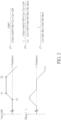
- FIG. 2 shows a gain and a phase contributed by the compensation circuit 140 according to one embodiment of the present invention.
- the first auxiliary amplifier 142, the second auxiliary amplifier 144, the capacitor Caz, and the resistors Ra and Raz are used to provide two poles and one zero for the transfer function of the multi-stage amplifier 100.
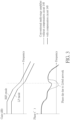
- FIG. 3 shows the phase compensation provided by using the compensation circuit 140.
- the multi-stage amplifier 100 can selectively operate in a high-fidelity mode (HiFi mode) or a low-power mode (LP mode).
- HiFi mode high-fidelity mode
- LP mode low-power mode
- the phase dip occurs at a frequency whose gain is 0dB (i.e., unity-gain frequency) due to the Zobel network 160.
- the compensation circuit 140 in the multi-stage amplifier 100 the zero Z1 is generated at low frequency to provide positive phase trapezoid to compensate the phase dip, so that the phase margin will be increased at these frequencies to stabilize the multi-stage amplifier 100.
- the resistor Raz and the capacitor Caz can be designed with smaller size to lower the manufacturing costs.
- the denominator of the equation (3) the denominator is dominated by "Caz*Gma*Ra*Raz", so if "Gma*Ra” is designed to have higher value by using active device, the "Caz*Raz” can be a smaller value, that is the chip area of the resistor Raz and the capacitor Caz can be smaller.
- the third auxiliary amplifier 146 within the compensation circuit 140 and the reference circuit 150 can be removed from the multi-stage amplifier 100. That is, the third amplifier stage 130 can directly receive the second signal V2 to generate the output signal Vout.
- This alternative design shall fall within the scope of the present invention.
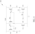
- FIG. 4 is a diagram illustrating the second amplifier stage 120, the compensation circuit 140 and the reference circuit 150 according to a first embodiment of the present invention.
- the second amplifier stage 120 is implemented by an N-type Metal Oxide Semiconductor Field Effect Transistor (MOSFET)
- the first auxiliary amplifier 142 is implemented by a P-type MOSFET
- the second auxiliary amplifier 144 is implemented by a P-type MOSFET
- the amplifier 152 within the reference circuit 150 is implemented by an N-type MOSFET.
- MOSFET Metal Oxide Semiconductor Field Effect Transistor
- FIG. 5 is a diagram illustrating the second amplifier stage 120, the compensation circuit 140 and the reference circuit 150 according to a second embodiment of the present invention.
- the second amplifier stage 120 is implemented by a P-type MOSFET
- the first auxiliary amplifier 142 is implemented by an N-type MOSFET
- the second auxiliary amplifier 144 is implemented by an N-type MOSFET
- the amplifier 152 within the reference circuit 150 is implemented by a P-type MOSFET.
- the resistor Ra can be implemented by using a P-type MOSFET or an N-type MOSFET.
- FIG. 6 is a diagram illustrating the second amplifier stage 120, the compensation circuit 140 and the reference circuit 150 according to a third embodiment of the present invention.
- the second amplifier stage 120 is implemented by an N-type MOSFET
- the first auxiliary amplifier 142 and the resistor Ra are implemented by a differential amplifier comprising transistors M1-M4 and a current source (Vref shown in FIG. 6 is a reference voltage)
- the second auxiliary amplifier 144 is implemented by a P-type MOSFET
- the amplifier 152 within the reference circuit 150 is implemented by an N-type MOSFET.
- FIG. 7 is a diagram illustrating the second amplifier stage 120, the compensation circuit 140 and the reference circuit 150 according to a second embodiment of the present invention.
- the second amplifier stage 120 is implemented by a P-type MOSFET
- the first auxiliary amplifier 142 and the resistor Ra are implemented by a differential amplifier comprising transistors M5-M8 and a current source (Vref shown in FIG. 7 is a reference voltage)
- the second auxiliary amplifier 144 is implemented by an N-type MOSFET
- the amplifier 152 within the reference circuit 150 is implemented by a P-type MOSFET.
- FIG. 8 is a diagram illustrating a multi-stage amplifier 800 according to one embodiment of the present invention.
- the multi-stage amplifier 800 comprises a plurality of amplifier stages such as a first amplifier stage 810, a second amplifier stage 820 and a third amplifier stage 830, a compensation circuit 840, a reference circuit 850, a first feedback capacitor Cm1 and a second feedback circuit Cm2, wherein the first feedback capacitor Cm1 is coupled between an output terminal of the third amplifier stage 830 and an output terminal of the first amplifier stage 810, and the second feedback capacitor Cm2 is coupled between the output terminal of the third amplifier stage 830 and an input terminal of the third amplifier stage 830.
- the multi-stage amplifier 800 is used to implement an output stage of a loud speaker, wherein a resistor RL and a capacitor CL shown in FIG. 8 are used to represent a load of the multi-stage amplifier 800, and a Zobel network comprising a capacitor Cz and a resistor Rz connected in series is coupled to an output node of the multi-stage amplifier 800 to damp high-frequency oscillations that might occur in the absence of loads in the loud speaker.
- the compensation circuit 840 comprises a first auxiliary amplifier 842, a second auxiliary amplifier 844, a resistor Ra, a resistor Raz and a capacitor Caz.
- An input terminal of the first auxiliary amplifier 842 is coupled to a first node of the capacitor Caz, and an output terminal of the first auxiliary amplifier 842 is coupled to a second node of the capacitor Caz.
- the resistor Raz is coupled between the output terminal of the first auxiliary amplifier 842 and a ground voltage.
- An input terminal of the second auxiliary amplifier 844 is coupled to the input terminal of the first auxiliary amplifier 842, and an output terminal of the second auxiliary amplifier 844 is coupled to an output terminal of the first amplifier stage 810.
- the resistor Raz is coupled between the input terminal and the output terminal of the second auxiliary amplifier 844.
- the symbols "Gma" and "Gmb1" are used to represent the gains of the first auxiliary amplifier 842 and the second auxiliary amplifier 844, respectively.
- the reference circuit 850 comprises an amplifier 852, a resistor Rb and a capacitor Cd.
- An input terminal of the amplifier 852 is coupled to a bias voltage Vb via the resistor Rb, and an output terminal of the amplifier 852 is coupled to the input terminal of the third amplifier stage 830.
- the capacitor Cd is coupled between the input terminal and the output terminal of the amplifier 852.
- the symbol "Gd2" is used to represent the gain of the amplifier 852.
- the first amplifier stage 810 receives an input signal Vin to generate a first signal V1
- the second amplifier stage 820 receives the first signal to generate a second signal V2
- the third amplifier stage 830 receives the second signal V2 to generate an output signal Vout.
- each of the first amplifier stage 810, the second amplifier stage 820 and the third amplifier stage 830 can be implemented by any suitable amplifier, the symbols "Gm1", “Gm2" and “Gm3" are used to represent gains of the first amplifier stage 810, the second amplifier stage 820 and the third amplifier stage 830, respectively. Because the amplifier stages used in the loud speaker are known by a person skilled in the art, the detailed circuits of these amplifier stages are omitted here.
- the compensation circuit 840 in the multi-stage amplifier 800 by using the compensation circuit 840 in the multi-stage amplifier 800, the zero Z1 is generated at low frequency to provide positive phase trapezoid to compensate the phase dip generated due to the Zobel network 860, so that the phase margin will be increased to stabilize the multi-stage amplifier 800.
- the resistor Raz and the capacitor Caz can be designed with smaller size to lower the manufacturing costs.
Landscapes
- Engineering & Computer Science (AREA)
- Power Engineering (AREA)
- Multimedia (AREA)
- Microelectronics & Electronic Packaging (AREA)
- Amplifiers (AREA)
Abstract
The present invention provides a multi-stage amplifier, wherein the multi-stage amplifier includes a plurality of amplifier stages and a compensation circuit. The compensation circuit is coupled to an output terminal of one of the plurality of amplifier stages, and the compensation circuit includes a first auxiliary amplifier, a capacitor, a second auxiliary amplifier, a first resistor and a second resistor. The capacitor is coupled between an input terminal and an output terminal of the first auxiliary amplifier. The second auxiliary amplifier is coupled to the first auxiliary amplifier. The first resistor is coupled between an input terminal and an output terminal of the second auxiliary amplifier. The second resistor is coupled between an output terminal of the first auxiliary amplifier and a ground voltage.
Description
- This application claims the benefit of
U.S. Provisional Application No. 63/489,790, filed on March 13th, 2023 - In order to damp high-frequency oscillations that might occur in the absence of loads in a loud speaker, a Zobel network having a resistor and a capacitor connected in series is usually placed on an output node of an audio amplifier of the loud speaker. However, the audio amplifier may be unstable due to the Zobel network if a bias current and a loop gain of output amplifier stage are reduced for a low power mode.
- It is therefore an objective of the present invention to provide a multi-stage amplifier, which has a compensation circuit to provide a zero at low frequency to compensate a phase dip generated due to the Zobel network, to solve the above-mentioned problems.
- According to one embodiment of the present invention, a multi-stage amplifier comprises a plurality of amplifier stages and a compensation circuit. The compensation circuit is coupled to an output terminal of one of the plurality of amplifier stages, and the compensation circuit comprises a first auxiliary amplifier, a capacitor, a second auxiliary amplifier, a first resistor and a second resistor. The capacitor is coupled between an input terminal and an output terminal of the first auxiliary amplifier. The second auxiliary amplifier is coupled to the first auxiliary amplifier. The first resistor is coupled between an input terminal and an output terminal of the second auxiliary amplifier. The second resistor is coupled between an output terminal of the first auxiliary amplifier and a ground voltage.
- These and other objectives of the present invention will no doubt become obvious to those of ordinary skill in the art after reading the following detailed description of the preferred embodiment that is illustrated in the various figures and drawings.
-
-
FIG. 1 is a diagram illustrating a multi-stage amplifier according to one embodiment of the present invention. -
FIG. 2 shows a gain and a phase contributed by the compensation circuit according to one embodiment of the present invention. -
FIG. 3 shows the phase compensation provided by using the compensation circuit. -
FIG. 4 is a diagram illustrating the second amplifier stage, the compensation circuit and the reference circuit according to a first embodiment of the present invention. -
FIG. 5 is a diagram illustrating the second amplifier stage, the compensation circuit and the reference circuit according to a second embodiment of the present invention. -
FIG. 6 is a diagram illustrating the second amplifier stage, the compensation circuit and the reference circuit according to a third embodiment of the present invention. -
FIG. 7 is a diagram illustrating the second amplifier stage, the compensation circuit and the reference circuit according to a fourth embodiment of the present invention. -
FIG. 8 is a diagram illustrating a multi-stage amplifier according to one embodiment of the present invention. - Certain terms are used throughout the following description and claims to refer to particular system components. As one skilled in the art will appreciate, manufacturers may refer to a component by different names. This document does not intend to distinguish between components that differ in name but not function. In the following discussion and in the claims, the terms "including" and "comprising" are used in an open-ended fashion, and thus should be interpreted to mean "including, but not limited to ...". The terms "couple" and "couples" are intended to mean either an indirect or a direct electrical connection. Thus, if a first device couples to a second device, that connection may be through a direct electrical connection, or through an indirect electrical connection via other devices and connections.
-
FIG. 1 is a diagram illustrating amulti-stage amplifier 100 according to one embodiment of the present invention. As shown inFIG. 1 , themulti-stage amplifier 100 comprises a plurality of amplifier stages such as afirst amplifier stage 110, asecond amplifier stage 120 and athird amplifier stage 130, acompensation circuit 140, areference circuit 150, a first feedback capacitor Cm1 and a second feedback circuit Cm2, wherein the first feedback capacitor Cm1 is coupled between an output terminal of thethird amplifier stage 130 and an output terminal of thefirst amplifier stage 110, and the second feedback capacitor Cm2 is coupled between the output terminal of thethird amplifier stage 130 and an input terminal of thethird amplifier stage 130. In this embodiment, themulti-stage amplifier 100 serves as an audio amplifier in a loud speaker, wherein a resistor RL and a capacitor CL shown inFIG. 1 are used to represent a load of themulti-stage amplifier 100, and a damping circuit such as a Zobelnetwork 160 comprising a capacitor Cz and a resistor Rz connected in series is coupled to an output node of themulti-stage amplifier 100 to damp high-frequency oscillations that might occur in the absence of loads in the loud speaker. - The
compensation circuit 140 comprises a firstauxiliary amplifier 142, a secondauxiliary amplifier 144, a thirdauxiliary amplifier 146, a resistor Ra, a resistor Raz and a capacitor Caz. An input terminal of the firstauxiliary amplifier 142 is coupled to a first node of the capacitor Caz, and an output terminal of the firstauxiliary amplifier 142 is coupled to a second node of the capacitor Caz, that is the capacitor Caz is coupled between the input terminal and the output terminal of the firstauxiliary amplifier 142. The resistor Raz is coupled between the output terminal of the firstauxiliary amplifier 142 and a ground voltage. An input terminal of the secondauxiliary amplifier 144 is coupled to the input terminal of the firstauxiliary amplifier 142, and an output terminal of the secondauxiliary amplifier 144 is coupled to an output terminal of thesecond amplifier stage 120. The resistor Raz is coupled between the input terminal and the output terminal of the secondauxiliary amplifier 144. The thirdauxiliary amplifier 146 has an input terminal coupled to an output terminal of thesecond amplifier stage 120, and has an output terminal coupled to the input terminal of thethird amplifier stage 130. In addition, the symbols "Gma", "Gmb1" and "Gmb2" are used to represent the gains of the firstauxiliary amplifier 142, the secondauxiliary amplifier 144 and the thirdauxiliary amplifier 146, respectively. - The
reference circuit 150 comprises anamplifier 152, a resistor Rb and a capacitor Cd. An input terminal of theamplifier 152 is coupled to a bias voltage Vb via the resistor Rb, and an output terminal of theamplifier 152 is coupled to the input terminal of thethird amplifier stage 130. The capacitor Cd is coupled between the input terminal and the output terminal of theamplifier 152. In addition, the symbol "Gd2" is used to represent the gain of theamplifier 152. - In the operation of the
multi-stage amplifier 100, thefirst amplifier stage 110 receives an input signal Vin (audio signal) to generate a first signal V1, and thesecond amplifier stage 120 receives the first signal to generate a second signal V2, thecompensation circuit 140 processes the second signal V2 to generate a third signal V3, and thethird amplifier stage 130 receives the third signal V3 to generate an output signal Vout. In the embodiment shown inFIG. 1 , each of thefirst amplifier stage 110, thesecond amplifier stage 120 and thethird amplifier stage 130 can be implemented by any suitable amplifier, the symbols "Gm1", "Gm2" and "Gm3" are used to represent gains of thefirst amplifier stage 110, thesecond amplifier stage 120 and thethird amplifier stage 130, respectively. Because the amplifier stages used in the loud speaker are known by a person skilled in the art, the detailed circuits of these amplifier stages are omitted here. - As described in the background of the present invention, the multi-stage amplifier may be unstable if a bias current and a loop gain are reduced for a low power mode. In order to solve this problem, the
multi-stage amplifier 100 shown inFIG. 1 uses thecompensation circuit 140 to provide a zero at low frequency to compensate the gain droop and phase dip, to increase a phase margin and stabilize themulti-stage amplifier 100. -
FIG. 2 shows a gain and a phase contributed by thecompensation circuit 140 according to one embodiment of the present invention. As shown inFIG. 2 , the firstauxiliary amplifier 142, the secondauxiliary amplifier 144, the capacitor Caz, and the resistors Ra and Raz are used to provide two poles and one zero for the transfer function of themulti-stage amplifier 100. Assuming that the firstauxiliary amplifier 142 is a transconductance amplifier having a gain "Gma", and the secondauxiliary amplifier 144 is a transconductance amplifier having a gain "Gmb1", frequencies of a first pole P1, a second pole P2 and a zero Z1 are as follows:


auxiliary amplifier 144 and the ground voltage. - Refer to
FIG. 2 andFIG. 3 together, whereinFIG. 3 shows the phase compensation provided by using thecompensation circuit 140. As shown inFIG. 2 andFIG. 3 , themulti-stage amplifier 100 can selectively operate in a high-fidelity mode (HiFi mode) or a low-power mode (LP mode). In the conventional multi-stage amplifier without thecompensation circuit 140, when the low-power mode is performed, the phase dip occurs at a frequency whose gain is 0dB (i.e., unity-gain frequency) due to the Zobelnetwork 160. In addition, by using thecompensation circuit 140 in themulti-stage amplifier 100, the zero Z1 is generated at low frequency to provide positive phase trapezoid to compensate the phase dip, so that the phase margin will be increased at these frequencies to stabilize themulti-stage amplifier 100. - In addition, by using the active device (i.e., the first auxiliary amplifier 142) and the resistor Ra in the
compensation circuit 140 to increase the impact of resistor Raz and the capacitor Caz on the zero point in the above equation (3), the resistor Raz and the capacitor Caz can be designed with smaller size to lower the manufacturing costs. Specifically, referring to the denominator of the equation (3), the denominator is dominated by "Caz*Gma*Ra*Raz", so if "Gma*Ra" is designed to have higher value by using active device, the "Caz*Raz" can be a smaller value, that is the chip area of the resistor Raz and the capacitor Caz can be smaller. - It is noted that, in the embodiment shown in
FIG. 1 , the thirdauxiliary amplifier 146 within thecompensation circuit 140 and thereference circuit 150 can be removed from themulti-stage amplifier 100. That is, thethird amplifier stage 130 can directly receive the second signal V2 to generate the output signal Vout. This alternative design shall fall within the scope of the present invention. -
FIG. 4 is a diagram illustrating thesecond amplifier stage 120, thecompensation circuit 140 and thereference circuit 150 according to a first embodiment of the present invention. In this embodiment, thesecond amplifier stage 120 is implemented by an N-type Metal Oxide Semiconductor Field Effect Transistor (MOSFET), the firstauxiliary amplifier 142 is implemented by a P-type MOSFET, the secondauxiliary amplifier 144 is implemented by a P-type MOSFET, and theamplifier 152 within thereference circuit 150 is implemented by an N-type MOSFET. -
FIG. 5 is a diagram illustrating thesecond amplifier stage 120, thecompensation circuit 140 and thereference circuit 150 according to a second embodiment of the present invention. In this embodiment, thesecond amplifier stage 120 is implemented by a P-type MOSFET, the firstauxiliary amplifier 142 is implemented by an N-type MOSFET, the secondauxiliary amplifier 144 is implemented by an N-type MOSFET, and theamplifier 152 within thereference circuit 150 is implemented by a P-type MOSFET. - In addition, in the embodiments shown in
FIG. 4 andFIG. 5 , the resistor Ra can be implemented by using a P-type MOSFET or an N-type MOSFET. -
FIG. 6 is a diagram illustrating thesecond amplifier stage 120, thecompensation circuit 140 and thereference circuit 150 according to a third embodiment of the present invention. In this embodiment, thesecond amplifier stage 120 is implemented by an N-type MOSFET, the firstauxiliary amplifier 142 and the resistor Ra are implemented by a differential amplifier comprising transistors M1-M4 and a current source (Vref shown inFIG. 6 is a reference voltage), the secondauxiliary amplifier 144 is implemented by a P-type MOSFET, and theamplifier 152 within thereference circuit 150 is implemented by an N-type MOSFET. -
FIG. 7 is a diagram illustrating thesecond amplifier stage 120, thecompensation circuit 140 and thereference circuit 150 according to a second embodiment of the present invention. In this embodiment, thesecond amplifier stage 120 is implemented by a P-type MOSFET, the firstauxiliary amplifier 142 and the resistor Ra are implemented by a differential amplifier comprising transistors M5-M8 and a current source (Vref shown inFIG. 7 is a reference voltage), the secondauxiliary amplifier 144 is implemented by an N-type MOSFET, and theamplifier 152 within thereference circuit 150 is implemented by a P-type MOSFET. -
FIG. 8 is a diagram illustrating amulti-stage amplifier 800 according to one embodiment of the present invention. As shown inFIG. 8 , themulti-stage amplifier 800 comprises a plurality of amplifier stages such as afirst amplifier stage 810, asecond amplifier stage 820 and athird amplifier stage 830, acompensation circuit 840, areference circuit 850, a first feedback capacitor Cm1 and a second feedback circuit Cm2, wherein the first feedback capacitor Cm1 is coupled between an output terminal of thethird amplifier stage 830 and an output terminal of thefirst amplifier stage 810, and the second feedback capacitor Cm2 is coupled between the output terminal of thethird amplifier stage 830 and an input terminal of thethird amplifier stage 830. In this embodiment, themulti-stage amplifier 800 is used to implement an output stage of a loud speaker, wherein a resistor RL and a capacitor CL shown inFIG. 8 are used to represent a load of themulti-stage amplifier 800, and a Zobel network comprising a capacitor Cz and a resistor Rz connected in series is coupled to an output node of themulti-stage amplifier 800 to damp high-frequency oscillations that might occur in the absence of loads in the loud speaker. - The
compensation circuit 840 comprises a firstauxiliary amplifier 842, a secondauxiliary amplifier 844, a resistor Ra, a resistor Raz and a capacitor Caz. An input terminal of the firstauxiliary amplifier 842 is coupled to a first node of the capacitor Caz, and an output terminal of the firstauxiliary amplifier 842 is coupled to a second node of the capacitor Caz. The resistor Raz is coupled between the output terminal of the firstauxiliary amplifier 842 and a ground voltage. An input terminal of the secondauxiliary amplifier 844 is coupled to the input terminal of the firstauxiliary amplifier 842, and an output terminal of the secondauxiliary amplifier 844 is coupled to an output terminal of thefirst amplifier stage 810. The resistor Raz is coupled between the input terminal and the output terminal of the secondauxiliary amplifier 844. In addition, the symbols "Gma" and "Gmb1" are used to represent the gains of the firstauxiliary amplifier 842 and the secondauxiliary amplifier 844, respectively. - The
reference circuit 850 comprises anamplifier 852, a resistor Rb and a capacitor Cd. An input terminal of theamplifier 852 is coupled to a bias voltage Vb via the resistor Rb, and an output terminal of theamplifier 852 is coupled to the input terminal of thethird amplifier stage 830. The capacitor Cd is coupled between the input terminal and the output terminal of theamplifier 852. In addition, the symbol "Gd2" is used to represent the gain of theamplifier 852. - In the operation of the
multi-stage amplifier 800, thefirst amplifier stage 810 receives an input signal Vin to generate a first signal V1, and thesecond amplifier stage 820 receives the first signal to generate a second signal V2, and thethird amplifier stage 830 receives the second signal V2 to generate an output signal Vout. In the embodiment shown inFIG. 8 , each of thefirst amplifier stage 810, thesecond amplifier stage 820 and thethird amplifier stage 830 can be implemented by any suitable amplifier, the symbols "Gm1", "Gm2" and "Gm3" are used to represent gains of thefirst amplifier stage 810, thesecond amplifier stage 820 and thethird amplifier stage 830, respectively. Because the amplifier stages used in the loud speaker are known by a person skilled in the art, the detailed circuits of these amplifier stages are omitted here. - Similar to the embodiment shown in
FIG. 1 ,FIG. 2 andFIG. 3 , by using thecompensation circuit 840 in themulti-stage amplifier 800, the zero Z1 is generated at low frequency to provide positive phase trapezoid to compensate the phase dip generated due to theZobel network 860, so that the phase margin will be increased to stabilize themulti-stage amplifier 800. In addition, by using the firstauxiliary amplifier 842 and the resistor Ra in thecompensation circuit 840 to increase the impact of resistor Raz and the capacitor Caz on the zero point in the above equation (3), the resistor Raz and the capacitor Caz can be designed with smaller size to lower the manufacturing costs. - Those skilled in the art will readily observe that numerous modifications and alterations of the device and method may be made while retaining the teachings of the invention. Accordingly, the above disclosure should be construed as limited only by the metes and bounds of the appended claims.
Claims (9)
- A multi-stage amplifier (100, 800), comprising:a plurality of amplifier stages (110, 120, 130, 810, 820, 830); anda compensation circuit (140, 840), coupled to an output terminal of one of the plurality of amplifier stages (110, 120, 130, 810, 820, 830), wherein the compensation circuit (140, 840) comprises:a first auxiliary amplifier (142, 842);a capacitor, wherein the capacitor (Caz) is coupled between an input terminal and an output terminal of the first auxiliary amplifier (142, 842);a second auxiliary amplifier (144, 844), coupled to the first auxiliary amplifier (142, 842);a first resistor, coupled between an input terminal and an output terminal of the second auxiliary amplifier (144, 844); anda second resistor, coupled between an output terminal of the first auxiliary amplifier (142, 842) and a ground voltage.
- The multi-stage amplifier (100, 800) of claim 1, wherein the input terminal of the first auxiliary amplifier (142, 842) is coupled to the input terminal of the second auxiliary amplifier (144, 844), and the output terminal of the second auxiliary amplifier (144, 844) is coupled to the output terminal of the one of the plurality of amplifier stages (110, 120, 130, 810, 820, 830).
- The multi-stage amplifier (100, 800) of claim 1, wherein the first auxiliary amplifier (142, 842) comprises at least an N-type Metal Oxide Semiconductor Field Effect Transistor, MOSFET, or a P-type MOSFET.
- The multi-stage amplifier (100, 800) of claim 3, wherein the second auxiliary amplifier (144, 844) comprises at least an N-type MOSFET or a P-type MOSFET.
- The multi-stage amplifier (100, 800) of claim 1, wherein the plurality of amplifier stages (110, 120, 130, 810, 820, 830) comprise:a first amplifier stage (110, 810), configured to receive an input signal to generate a first signal;a second amplifier stage (120, 820), configured to receive the first signal to generate a second signal; anda third amplifier stage (130, 830);wherein the compensation circuit (140, 840) generates a third signal according to the second signal, wherein the third signal is inputted to the third amplifier stage (130, 830) .
- The multi-stage amplifier (100, 800) of claim 5, wherein the input terminal of the first auxiliary amplifier (142, 842) is coupled to the input terminal of the second auxiliary amplifier (144, 844), and the output terminal of the second auxiliary amplifier (144, 844) is coupled to an output terminal of the second amplifier stage (120, 820); and the compensation circuit (140, 840) further comprises:
a third auxiliary amplifier (146), configured to receive the second signal to generate the third signal. - The multi-stage amplifier (100, 800) of claim 1, wherein the plurality of amplifier stages comprise:a first amplifier stage (110, 810), configured to receive an input signal to generate a first signal;a second amplifier stage (120, 820), configured to receive the first signal to generate a second signal; anda third amplifier stage (130, 830), configured to receive the second signal to generate an output signal;wherein the compensation circuit (140, 840) is coupled to an output terminal of the first amplifier stage (110, 810).
- The multi-stage amplifier (100, 800) of claim 7, wherein the input terminal of the first auxiliary amplifier (142, 842) is coupled to the input terminal of the second auxiliary amplifier (144, 844), and the output terminal of the second auxiliary amplifier (144, 844) is coupled to the output terminal of the first amplifier stage (110, 810).
- The multi-stage amplifier (100, 800) according to any one of the preceding claims, wherein the multi-stage amplifier (100, 800) is an audio amplifier configured to receive an audio signal.
Applications Claiming Priority (2)
| Application Number | Priority Date | Filing Date | Title |
|---|---|---|---|
| US202363489790P | 2023-03-13 | 2023-03-13 | |
| US18/433,468 US20240313706A1 (en) | 2023-03-13 | 2024-02-06 | Area-efficient compensation circuit for low-power multi-stage amplifier |
Publications (1)
| Publication Number | Publication Date |
|---|---|
| EP4439979A1 true EP4439979A1 (en) | 2024-10-02 |
Family
ID=90365183
Family Applications (1)
| Application Number | Title | Priority Date | Filing Date |
|---|---|---|---|
| EP24163199.3A Pending EP4439979A1 (en) | 2023-03-13 | 2024-03-13 | Area-efficient compensation circuit for low-power multi-stage amplifier |
Country Status (3)
| Country | Link |
|---|---|
| US (1) | US20240313706A1 (en) |
| EP (1) | EP4439979A1 (en) |
| TW (1) | TWI889232B (en) |
Citations (2)
| Publication number | Priority date | Publication date | Assignee | Title |
|---|---|---|---|---|
| US6208206B1 (en) * | 1999-02-11 | 2001-03-27 | The Hong Kong University Of Science And Technology | Frequency compensation techniques for low-power multistage amplifiers |
| EP3745590A1 (en) * | 2019-05-28 | 2020-12-02 | MediaTek Inc. | Amplifier circuit with high-order damping circuit and the high-order damping circuit |
Family Cites Families (3)
| Publication number | Priority date | Publication date | Assignee | Title |
|---|---|---|---|---|
| US7898333B2 (en) * | 2008-05-23 | 2011-03-01 | Teledyne Scientific & Imaging, Llc | Operational amplifier |
| CN103580615B (en) * | 2013-10-22 | 2016-06-29 | 中国科学院半导体研究所 | Signal amplification circuit |
| CN115001423A (en) * | 2022-05-16 | 2022-09-02 | 上海交通大学 | Sensing amplifying circuit for collecting multiple physiological electric signals |
-
2024
- 2024-02-06 US US18/433,468 patent/US20240313706A1/en active Pending
- 2024-03-08 TW TW113108614A patent/TWI889232B/en active
- 2024-03-13 EP EP24163199.3A patent/EP4439979A1/en active Pending
Patent Citations (2)
| Publication number | Priority date | Publication date | Assignee | Title |
|---|---|---|---|---|
| US6208206B1 (en) * | 1999-02-11 | 2001-03-27 | The Hong Kong University Of Science And Technology | Frequency compensation techniques for low-power multistage amplifiers |
| EP3745590A1 (en) * | 2019-05-28 | 2020-12-02 | MediaTek Inc. | Amplifier circuit with high-order damping circuit and the high-order damping circuit |
Non-Patent Citations (2)
| Title |
|---|
| SHIN HONGSEOK ET AL: "An Energy-Efficient Three-Stage Amplifier Achieving a High Unity-Gain Bandwidth for Large Capacitive Loads Without Using a Compensation Zero", IEEE SOLID-STATE CIRCUITS LETTERS, IEEE, vol. 3, 6 November 2020 (2020-11-06), pages 530 - 533, XP011823461, DOI: 10.1109/LSSC.2020.3036496 * |
| ZUSHU YAN ET AL: "A 0.016-mm $^{2}$ 144- $\mu$ W Three-Stage Amplifier Capable of Driving 1-to-15 nF Capacitive Load With $> $ 0.95-MHz GBW", IEEE JOURNAL OF SOLID-STATE CIRCUITS, IEEE, USA, vol. 48, no. 2, 1 February 2013 (2013-02-01), pages 527 - 540, XP011489702, ISSN: 0018-9200, DOI: 10.1109/JSSC.2012.2229070 * |
Also Published As
| Publication number | Publication date |
|---|---|
| US20240313706A1 (en) | 2024-09-19 |
| TW202437685A (en) | 2024-09-16 |
| TWI889232B (en) | 2025-07-01 |
Similar Documents
| Publication | Publication Date | Title |
|---|---|---|
| EP2328056B1 (en) | Low-dropout linear regulator (LDO), method for providing an LDO and method for operating an LDO | |
| CN100498634C (en) | Voltage regulator | |
| EP1569062B1 (en) | Efficient frequency compensation for linear voltage regulators | |
| US6208206B1 (en) | Frequency compensation techniques for low-power multistage amplifiers | |
| US20070046378A1 (en) | Operational amplifier output stage and method | |
| EP1468489B1 (en) | Operational amplifier having improved input offset performance | |
| EP3089360B1 (en) | Apparatus and method for improving power supply rejection ratio | |
| US20240313706A1 (en) | Area-efficient compensation circuit for low-power multi-stage amplifier | |
| US6812778B1 (en) | Compensating capacitive multiplier | |
| US20050110571A1 (en) | Variable gain amplifier | |
| US8624671B2 (en) | Audio amplifying circuit with improved noise performance | |
| EP2371059B1 (en) | Operational transconductance amplifier having two amplification stages | |
| US6734720B2 (en) | Operational amplifier in which the idle current of its output push-pull transistors is substantially zero | |
| US6741133B2 (en) | High output amplifier for stable operation | |
| EP4290772A1 (en) | Low power clock buffer architecture | |
| US20080226100A1 (en) | Microphone Amplification Arrangement and Integrated Circuit Therefor | |
| US20030218503A1 (en) | High gain amplifier with rail to rail range and frequency compensation | |
| CN118646379A (en) | Multi-stage amplifier and audio processing device | |
| JPS59207712A (en) | Amplifier | |
| EP0812063A2 (en) | Gain-variable amplifier having small DC output deviation and small distortion | |
| EP0043699B1 (en) | Operational amplifier | |
| JP4244890B2 (en) | Piezoelectric oscillation circuit | |
| CN110244811B (en) | Voltage regulator without external output capacitor | |
| US6407636B1 (en) | Stability control multistage operational amplifier | |
| US20250183856A1 (en) | Output load aware compensation scheme for multi-stage amplifier |
Legal Events
| Date | Code | Title | Description |
|---|---|---|---|
| PUAI | Public reference made under article 153(3) epc to a published international application that has entered the european phase |
Free format text: ORIGINAL CODE: 0009012 |
|
| STAA | Information on the status of an ep patent application or granted ep patent |
Free format text: STATUS: THE APPLICATION HAS BEEN PUBLISHED |
|
| AK | Designated contracting states |
Kind code of ref document: A1 Designated state(s): AL AT BE BG CH CY CZ DE DK EE ES FI FR GB GR HR HU IE IS IT LI LT LU LV MC ME MK MT NL NO PL PT RO RS SE SI SK SM TR |
|
| STAA | Information on the status of an ep patent application or granted ep patent |
Free format text: STATUS: REQUEST FOR EXAMINATION WAS MADE |
|
| 17P | Request for examination filed |
Effective date: 20250327 |