EP4439862A1 - Rf module for antenna, and antenna apparatus comprising same - Google Patents
Rf module for antenna, and antenna apparatus comprising same Download PDFInfo
- Publication number
- EP4439862A1 EP4439862A1 EP22899001.6A EP22899001A EP4439862A1 EP 4439862 A1 EP4439862 A1 EP 4439862A1 EP 22899001 A EP22899001 A EP 22899001A EP 4439862 A1 EP4439862 A1 EP 4439862A1
- Authority
- EP
- European Patent Office
- Prior art keywords
- filter
- unit
- filter part
- antenna
- board
- Prior art date
- Legal status (The legal status is an assumption and is not a legal conclusion. Google has not performed a legal analysis and makes no representation as to the accuracy of the status listed.)
- Pending
Links
Images







Classifications
-
- H—ELECTRICITY
- H01—ELECTRIC ELEMENTS
- H01Q—ANTENNAS, i.e. RADIO AERIALS
- H01Q25/00—Antennas or antenna systems providing at least two radiating patterns
- H01Q25/001—Crossed polarisation dual antennas
-
- H—ELECTRICITY
- H01—ELECTRIC ELEMENTS
- H01Q—ANTENNAS, i.e. RADIO AERIALS
- H01Q1/00—Details of, or arrangements associated with, antennas
- H01Q1/12—Supports; Mounting means
- H01Q1/22—Supports; Mounting means by structural association with other equipment or articles
- H01Q1/24—Supports; Mounting means by structural association with other equipment or articles with receiving set
- H01Q1/241—Supports; Mounting means by structural association with other equipment or articles with receiving set used in mobile communications, e.g. GSM
- H01Q1/246—Supports; Mounting means by structural association with other equipment or articles with receiving set used in mobile communications, e.g. GSM specially adapted for base stations
-
- H—ELECTRICITY
- H01—ELECTRIC ELEMENTS
- H01Q—ANTENNAS, i.e. RADIO AERIALS
- H01Q15/00—Devices for reflection, refraction, diffraction or polarisation of waves radiated from an antenna, e.g. quasi-optical devices
- H01Q15/14—Reflecting surfaces; Equivalent structures
-
- H—ELECTRICITY
- H01—ELECTRIC ELEMENTS
- H01Q—ANTENNAS, i.e. RADIO AERIALS
- H01Q21/00—Antenna arrays or systems
- H01Q21/24—Combinations of antenna units polarised in different directions for transmitting or receiving circularly and elliptically polarised waves or waves linearly polarised in any direction
Definitions
- the present disclosure relates to an RF module for an antenna and an antenna apparatus including the same, and more particularly, to an RF module for an antenna, an RF module assembly, and an antenna apparatus including the same, wherein a radiation element module and an RF element are fully separated from a main board, but are disposed to be exposed to an ambient air ahead thereof and which can solve a difficulty in a heat dissipation design toward on the front side thereof having a conventional radiation element.
- a base station antenna including a relay that is used in a mobile communication system has various forms and structures.
- the base station antenna has a structure in which multiple radiation elements are properly disposed on at least one reflection plate that stands upright in a length direction thereof.
- MIMO multi-input & multi-output
- a method of plating a radiation element consisting of a dielectric board made of a plastic or ceramic material and coupling the radiating element to a printed circuit board (PCB) through soldering is widely used.
- FIG. 1 is an exploded perspective view of illustrating an example of an antenna apparatus according to a conventional technology.
- an antenna apparatus 1 in an antenna apparatus 1 according to the conventional technology, multiple radiation elements 35 are arranged on the front side of an antenna housing body 10, that is, a beam output direction, so that beams are output in a desired direction to facilitate beamforming.
- a radome 50 is mounted at the front end of the antenna housing body 10 with the multiple radiation elements 35 interposed therebetween.
- the antenna apparatus 1 is provided in the form of a thin rectangular parallelepiped enclosure having a front opened, and includes the antenna housing body 10 in which multiple heat dissipation pins 11 have been integrally formed, a main board 20 that is stacked and disposed on a rear surface of the antenna housing body 10 therein, and an antenna board 30 that is stacked and disposed on a front surface of the antenna housing body 10 therein, at the rear of the enclosure.
- the patch type radiation elements or dipole type radiation elements 35 may be mounted on a front surface of the antenna board 30.
- the radome 50 that enables radiation from the radiation elements 35 to be smoothly performed, while protecting parts therein against the outside, may be installed in front of the antenna housing body 10.
- the example 1 of the antenna apparatus according to the conventional technology has a structure in which various digital elements (an FPGA element, etc.) and analog amplification elements (a PA element, an LNA element, etc.) are intensively mounted on the main board 20 so that heat is dissipated toward the back of the antenna housing body 10.
- various digital elements an FPGA element, etc.
- analog amplification elements a PA element, an LNA element, etc.
- the LNA element among the analog amplification elements, has problems in that it increases the density of installation distributions for the main board of other heat-generation elements and has a cause to directly degrade performance due to the generation of heat from other heat-generation elements because the LNA element has a small amount of heat generation and is also mounted on the main board 20.
- a common antenna apparatus has a passive inter-modulation (PIM) problem.
- PIM is a spurious signal that is generated due to a non-linear characteristic of a passive element, and refers to a phenomenon in which the spurious signal deteriorates communication quality by reducing a signal to noise characteristic on a communication path.
- the PIM characteristic within equipment of a distributed antenna system is maintained with predetermined quality or higher upon production, but may have a PIM problem due to a passive element that is used in a distribution network up to the final antenna at the rear end of an antenna port of remote equipment in the field.
- an antenna apparatus is designed to have a structure in which internal parts, such as an antenna element, are modulated and mounted, the PIM problem becomes great compared to the integrated mounting case if the modules are not stably fixed.
- the present disclosure has been intended to solve the aforementioned technical problems, and an object of the present disclosure is to provide an RF module for an antenna, which is capable of a heat distribution by separating an LNA board part on which an LNA element having a slightly small amount of heat generation, among heat-generation elements, has been mounted from a main board and coupling the LNA board part to the unit RF filter body side, and an antenna apparatus including the same.
- another object of the present disclosure is to provide an RF module for an antenna, which can improve the productivity of a product by modulating a radiation element part, a left filter part, a right filter part, and an amplification element part so that the radiation element part, the left filter part, the right filter part, and the amplification element part can be manufactured in a module unit and assembled on at least any one of front surface, left and right sides, and upper and lower surfaces of an RF filter body, and an antenna apparatus including the same.
- Still another object of the present disclosure is to provide an antenna apparatus capable of stably fixing and supporting an RF module for an antenna which is manufactured in a modulation unit so that the PIM characteristic can be maintained.
- An embodiment of an RF module for an antenna includes a unit RF filter body arranged on a front surface of a main board, a radiation element part disposed on a front surface of the unit RF filter body, and a reflector panel configured to form the front surface of the unit RF filter body, formed to be wider than the area of a vertical cross section of the unit RF filter body, and configured to ground (GND) the radiation element part.
- a left filter part and a right filter part in which multiple cavities each opened to the outside on left and right sides thereof have been formed and which each have a resonator embedded in each cavity and perform different frequency filtering are provided on left and right sides of the unit RF filter body, respectively.
- the left filter part and the right filter part are electrically connected to the radiation element part through the reflector panel.
- a pair of pin terminal installation holes through which a third connection pin terminal configured to mediate the transfer of transmission signals and reception signal of the left filter part, the right filter part, and the radiation element part is installed may be formed in the reflector panel.
- the radiation element part may be provided to generate one polarization, among at least two multi-polarizations.
- the radiation element part includes a base panel disposed on a front surface of the reflector panel, a power feeding base attached to the base panel and electrically connected to the left filter part and the right filter part, and a director panel for radiation which is provided at a front end of the power feeding base.
- connection pin terminal may be soldered and fixed to the base panel.
- the RF module may further include an amplification element part including an LNA board part that is provided on any one of an upper surface and lower surface that are front and rear thickness parts of the unit RF filter body and on which at least one analog amplification element has been mounted.
- an amplification element part including an LNA board part that is provided on any one of an upper surface and lower surface that are front and rear thickness parts of the unit RF filter body and on which at least one analog amplification element has been mounted.
- an LNA board part may be disposed in a board installation space provided on an upper surface or a lower surface that forms a front and rear thickness part of the unit RF filter body.
- the LNA board part may be electrically connected to each of the cavities of the left filter part and right filter part formed on the left and right sides of the unit RF filter body.
- a male socket part to be coupled in a socket pin coupling way with respect to the main board may be formed in the LNA board part.
- a penetration slit through which the male socket part of the LNA board part passes may be formed in a board installation space.
- At least one LNA element configured to amplify a reception signal that is received via the left filter part or the right filter part from the radiation element part may be mounted on the LNA board part.
- At least one PA element except the LNA element may be mounted on the main board. Heat generated from the at least one PA element may be discharged to the back of an antenna housing on which the main board has been stacked.
- a pin installation hole that penetrates through the board installation space, the cavity of the left filter part, and the cavity of the right filter part may be formed in the unit RF filter body.
- the LNA board part, the left filter part, and the right filter part may be electrically connected by at least one second connection pin terminal installed in each pin installation hole.
- the second connection pin terminal may be soldered and fixed to the LNA board part.
- At least one input and output port for transferring transmission signals through the left filter part and the right filter part may be provided in the unit RF filter body.
- the main board, the left filter part, and the right filter part may be electrically connected to the at least one input and output port through a medium of the at least one first connection pin terminal.
- the at least one first connection pin terminal may be soldered and fixed to the front surface of the main board
- An antenna apparatus including an RF module for an antenna includes an antenna housing part formed in a form of an enclosure having a front surface opened, a main board stacked and disposed to be closely attached to an inside of the antenna housing part, and multiple RF modules for an antenna, which are arranged on a front surface of the main board.
- the multiple RF modules for an antenna may include a unit RF filter body arranged on the front surface of the main board, a radiation element part disposed on a front surface of the unit RF filter body, and a reflector panel configured to form the front surface of the unit RF filter body, formed to be wider than the area of a vertical cross section of the unit RF filter body, and configured to ground (GND) the radiation element part.
- a left filter part and a right filter part in which multiple cavities each opened to the outside on left and right sides thereof have been formed and which each have a resonator embedded in each cavity and perform different frequency filtering may be provided on left and right sides of the unit RF filter body, respectively.
- the left filter part and the right filter part may be electrically connected to the radiation element part through the reflector panel.
- the multiple RF modules for an antenna may each further include an amplification element part including an LNA board part that is provided on any one of an upper surface and lower surface that are front and rear thickness parts of the unit RF filter body and on which at least one analog amplification element has been mounted.
- the radiation element part may include a base panel disposed on a front surface of the reflector panel.
- the left filter part and the right filter part may be soldered and fixed to the main board so that the left filter part and the right filter part are electrically connected to the main board through a medium of at least one first connection pin terminal.
- the left filter part and the right filter part may be soldered and fixed to an LNA board part so that the left filter part and the right filter part are electrically connected to the LNA board part through a medium of at least one second connection pin terminal.
- the left filter part and the right filter part may be soldered and fixed to the base panel so that the left filter part and the right filter part are electrically connected to the base panel through a medium of at least one third connection pin terminal.
- the antenna apparatus may further include a fixing member having both left and right ends fixed to left and right side walls of the antenna housing part and configured to fix the unit RF filter body.
- the fixing member may be made of a non-conductive material.
- the following various effects can be achieved.
- antenna apparatus 110 antenna housing part 110S: internal space 111: rear heat dissipation pin 120: main board 125: female socket part 130: PSU board part 140: RFIC board part 150: surge board part 200: RF module for an antenna 210: unit RF filter body 220: radiation element part 230: amplification element part 270: reflector panel 287: input and output port
- FIG. 2 is a perspective view illustrating an antenna apparatus according to an embodiment of the present disclosure.
- FIG. 3 is a general exploded perspective view of FIG. 2 .
- FIG. 4 is an exploded perspective view for describing a process of installing a main board of an RF module for an antenna, among the components of FIG. 2 .
- FIG. 5 is an exploded perspective view for describing a process of installing a fixing member, among the components of FIG. 2 .
- an antenna apparatus 100 includes an antenna housing part 110 that forms external appearances of left and right sides and rear side of the antenna apparatus 100, and a radome panel 300 that forms an external appearance of the front of the antenna apparatus 100, that is provided to shield an opened front surface of the antenna housing part 110, and that protects internal parts (including a main board 120 and an RF module 200 for an antenna described later) provided in an internal space 110S of the antenna housing part 110 against the outside.
- an antenna housing part 110 that forms external appearances of left and right sides and rear side of the antenna apparatus 100
- a radome panel 300 that forms an external appearance of the front of the antenna apparatus 100, that is provided to shield an opened front surface of the antenna housing part 110, and that protects internal parts (including a main board 120 and an RF module 200 for an antenna described later) provided in an internal space 110S of the antenna housing part 110 against the outside.
- the antenna apparatus 100 further includes the main board 120 closely installed in the internal space 110S of the antenna housing part 110, a PSU board part 130 disposed on an upper side of the main board 120, an RFIC board part 140 provided between the pair of main boards 120, and a surge board part 150 at a lower part of the main board 120, and may further include the radio frequency module 200 (hereinafter abbreviated as the "RF module") for an antenna that is stacked and disposed a front surface of the main board 120.
- RF module radio frequency module
- the antenna housing part 110 may play a role of mediating the coupling of a pillar pole that is provided to install the antenna apparatus 100.
- the antenna housing part 110 is generally provided as a metal material having excellent thermal conductivity in order to be advantageous for heat dissipation according to thermal conduction, and may be formed in the form of a rectangular enclosure having a thickness in forward and backward directions to the extent that the front end of the RF module 200 described later can be accommodated therein.
- the inside of the antenna housing part 110 may be formed in a form in which the inside of the antenna housing part is matched with an external protrusion shape by a digital element (an FPGA element, etc.) mounted on a rear surface of the main board 120 and/or a PSU element mounted on a rear surface of the PSU board part 130 and surge part elements mounted on a rear surface of the surge board part 150.
- a digital element an FPGA element, etc.
- PSU element mounted on a rear surface of the PSU board part 130
- surge part elements mounted on a rear surface of the surge board part 150.
- a female socket part 125 to which a male socket part 235 formed in an LNA board part 231 of an amplification element part 230, among components of the RF module 200 for an antenna, which are manufactured in a module unit described later, is coupled in a socket pin coupling way may be provided on the front surface of the main board 120
- a pin coupling part 123 to which first connection pin terminals 281 of a left filter part 240A and a right filter part 240B, among components of the RF module 200 for an antenna, is coupled in a terminal pin coupling way may be provided on the front surface of the main board.
- handle parts which may be held by a worker so that the worker can carry the antenna apparatus 100 according to an embodiment of the present disclosure or can easily mount a pillar pole (not illustrated) manually on the spot may be further installed on both left and right sides of the antenna housing part 110.
- outside mounting members 400 for a cable connection with a base station apparatus not illustrated and the tuning of internal parts may be assembled with the outside of the bottom of the antenna housing part 110 through the antenna housing part.
- the outside mounting members 400 are provided in the form of at least one optical cable connection terminal (socket). Connection terminals of coaxial cables (not illustrated) may be mutually connected to connection terminals of the outside mounting members, respectively.
- multiple rear heat dissipation pins 111 may be integrally formed on a rear surface of the antenna housing part 110 so that the multiple rear heat dissipation pins have a predetermined pattern shape.
- the multiple rear heat dissipation pins 111 do not need to be essentially integrally formed on the rear surface of the antenna housing part 110. It may be said to be natural that the multiple rear heat dissipation pins may be manufactured as individual parts and may be coupled to the rear surface of the antenna housing part 110 in various coupling ways including a laser welding method.
- heat that is generated from each of heat-generation elements of the main board 120, the PSU board 130, the RFIC board part 140, and the surge board part 150 installed in the internal space 110S of the antenna housing part 110 may be directly discharged backward through the multiple rear heat dissipation pins 111.
- the multiple rear heat dissipation pins 111 are upward slantly disposed toward a left end and a right end thereof on the basis of an upper and lower portion that connects the middle of a left and right width thereof, and may be designed so that pieces of heat that are discharged to the back of the antenna housing part 110 form an upcurrent distributed in the horizontal direction and are distributed more rapidly.
- a shape of the multiple rear heat dissipation pins 111 is not essentially limited thereto.
- the multiple rear heat dissipation pins 111 may be adopted so that the multiple rear heat dissipation pins are formed in parallel at the left end and the right end in the blower fan module that is disposed at the center thereof in order for discharged heat to be discharged more rapidly by the blower fan module.
- the radome panel 300 is coupled to a front end of the antenna housing part 110, but a hook coupling part 310 that is formed along the edge of the radome panel 300 may be hook-coupled to the front locking rib (a reference numeral not indicated) side of the antenna housing part 110.
- a waterproof gasket ring 180 made of a rubber material may be interposed between the edge of the front end of the antenna housing part 110 and the radome panel 300.
- the waterproof gasket ring 180 may perform a sealing function while being elastically deformed by a coupling force that is provided upon hook-coupling with the antenna housing part 110 of the radome panel 300.
- the antenna apparatus 100 may further include fixing members 280 for fixing a unit RF filter body 210 of each RF module 200 upon installation of the RF module 200 for an antenna.
- the fixing member 280 may be fixed as both left and right ends of the fixing member are disposed within multiple left and right penetration holes 171 provided to penetrate left and right side walls of the antenna housing part 110 and multiple assembly screws 173 are fastened to screw fastening holes 281 formed at both left and right ends of the fixing member through the multiple left and right penetration holes 171 from the outside.
- each of the multiple left and right penetration holes 171 may be shielded from the outside by attaching a separate shielding film 175 thereto.
- multiple module fixing screw holes 283 may be formed in the fixing member 280 so that the multiple module fixing screw holes are horizontally spaced apart from each other.
- Multiple assembly screws (not illustrated) may be fastened to module fixing screw fastening holes 275 formed in a reflector panel 270, among components of the RF module 200 assembled in the internal space 110S of the antenna housing part 110. Accordingly, each RF module 200 can be stably fixed.
- PIM passive inter-modulation
- the PIM phenomenon is a phenomenon that occurs due to a kind of radio wave interference, and major causes thereof include radio waves of several frequencies and rusty metal, in general.
- the PIM phenomenon is not a problem that essentially occurs by the two factors only.
- the non-linearity an error of a metal contact point
- contraction resistance that is generated between electrical connection elements due to a fine twist attributable to the skewed and concentrated heat generation of heat-generation elements that operate for an operation of the antenna housing part may become a cause of the PIM problem.
- a non-conductive material e.g., a plastic resin-based material
- a plastic resin-based material is adopted as the fixing member 280 so that the PIM influence is minimized and the influence of the reflector panel 270 described later on a ground (GND) role is minimized.
- a plastic resin-based material is also adopted as the multiple assembly screws (not illustrated).
- the antenna apparatus 100 may further include a buffering part made of a silicon rubber material, which is attached to a front end of the fixing member 280.
- the buffering part may play a role of reducing an internal impact between parts by being seated and installed in the fixing member 280 that fixes each unit RF filter body 210.
- each RF module is modulated and manufactured as described above and a coupling force between the main board 110 and each RF module 200 depends on a very weak coupling force between the male socket part 235 of the LNA board part 231 and the first connection pin terminals 281 of the RF filter body part 210 as described later. Accordingly, the PIM problem may be solved by using the fixing member 280 that firmly fixes and supports each RF module 200. This is described later while describing each component of the RF module 200 in detail.
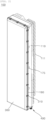
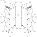
- FIGS. 6A and 6B are perspective views illustrating a front part and rear part of the RF module for an antenna, among the components of FIG. 2 .
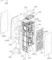
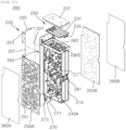
- FIGS. 7A to 7D are exploded perspective views in the left direction and right direction of FIGS. 6A and 6B .
- an embodiment of the RF module 200 for an antenna may include the unit RF filter body 210 arranged on the front surface of the main board 120, a radiation element part 220 disposed on a front surface of the unit RF filter body 210, and the reflector panel 270 that forms the front surface of the unit RF filter body 210, that is formed to be wider than the area of a vertical cross section of the unit RF filter body 210, and that grounds (GND) the radiation element part 220.
- the unit RF filter body 210 arranged on the front surface of the main board 120
- a radiation element part 220 disposed on a front surface of the unit RF filter body 210
- the reflector panel 270 that forms the front surface of the unit RF filter body 210, that is formed to be wider than the area of a vertical cross section of the unit RF filter body 210, and that grounds (GND) the radiation element part 220.
- multiple cavities C1 and C2 that have been opened to the outside on the left and right sides thereof are formed on the left and right sides of the unit RF filter body 210, respectively.
- the left filter part 240A and the right filter part 240B each having a resonator R embedded therein and performing different frequency filtering may be provided within the cavities C1 and C2, respectively.
- the left filter part 240A and the right filter part 240B are described by defining that the left filter part and the right filter part are disposed on the left and right sides on the basis of a front direction.
- the resonator R may be a resonator having a bar shape, but a shape thereof is not limited thereto.
- the resonator may also be made of various materials, such as dielectrics such as ceramic, or metal.
- the left filter part 240A and the right filter part 240B may be designed as filters for a frequency band of 2.4G and a frequency band of 5G, respectively, and may implement a dual band antenna by one RF module 200.
- the radiation element part 220 may be provided to generate two or more multiple polarizations.
- the radiation element part 220 that has implemented dual polarization, among multiple polarizations, is described in detail as an example.
- the RF module may include base panels 221 each disposed on a front surface of the reflector panel 270, power feeding bases 223 attached to the base panels 221, electrically connected to the left filter part 240A and the right filter part 240B, and each intersected and arranged in an "X" shape, and director panels 225 for radiation, which are provided at a front end of the power feeding base 223.
- the power feeding base 223 has been limited to being intersected and arranged in the "X" shape with respect to the base panel 221, but the present disclosure is not essentially thereto and does not exclude the array of the power feeding base in a " " shape, an "H” shape, and a "+" shape.
- the director panel 225 for radiation is formed in an approximately square shape.
- the power feeding base 223 is disposed to diagonally support each edge portion of the director panel 225 for radiation, and each feeding end thereof is extended to be disposed at a central part of each side of the director panel 225 for radiation and fed and connected. Accordingly, each power feeding base 223 may implement dual polarization by generating each polarization.
- the base panels 221 may be electrically connected to mediate the transfer of transmission signals from the left filter part 240A and the right filter part 240B formed on the left and right sides of the unit RF filter body 210, respectively, and the transfer of a reception signal from the director panel 225 for radiation.
- An electrical connection mechanism between the base panel 221 and each of the filter parts 240A and 240B is described more specifically later.
- the radiation element part 220 is limited to being described as any one of the patch type and the dipole type, but the present disclosure is not essentially limited thereto. It is to be noted that the application of an air strip type antenna is not excluded.
- the RF module 200 for an antenna may further include the amplification element part 230 including the LNA board part 231 that is provided on any one of an upper surface and a lower surface, that is, front and rear thickness parts of the unit RF filter body 210, and on which at least one analog amplification element (not illustrated) has been mounted.
- the amplification element part 230 including the LNA board part 231 that is provided on any one of an upper surface and a lower surface, that is, front and rear thickness parts of the unit RF filter body 210, and on which at least one analog amplification element (not illustrated) has been mounted.
- the amplification element part 230 may include the LNA board part 231 in a board installation space 230S that is provided on any one of the upper surface and the lower surface that form the front and rear thickness parts of the unit RF filter body 210.
- At least one LNA element (not illustrated) having a relatively small amount of heat generation, among analog amplification elements, and playing a role of amplifying a reception signal may be mounted on the LNA board part 231.
- an RF module is an array of analog RF parts.
- analog amplification elements that amplify an RF signal are mounted on the amplification element part 230.
- the RF module 200 according to an embodiment of the present disclosure, only LNA elements having relatively small heat generation, among analog amplification elements, have been separated from the main board 120 and designed to be included in the unit RF filter body 210.
- the left filter part 240A and the right filter part 240B are each an RF part for frequency-filtering an input RF signal into a desired frequency band.
- the radiation element part 220 may be defined as an RF part that plays a role of receiving and transmitting RF signals.
- the LNA board part 231 may be electrically connected to the cavities C1 and C2 of the left filter part 240A and the right filter part 240B that are formed on the left and right sides of the unit RF filter body 210, respectively.
- An electrical connection mechanism between the LNA board part 231 and each of the filter parts 240A and 240B is described more specifically later.
- the board installation space 230S in which the LNA board part 231 has been installed may be shielded by using an amplification part cover panel 237.
- An amplification part heat sink pin (not illustrated) that discharges heat within the board installation space 230S in a thermal conduction way may be integrally formed on an outside surface of the amplification part cover panel 237. The heat that is discharged through the amplification part heat sink pin may be discharged to the outside through a lateral part of the antenna housing part 110.
- An embodiment in which only the LNA elements, among multiple analog amplification elements mounted and disposed in the existing main board 120 on the side of the unit RF filter body 210, are separately separated and provided as the amplification element part 230 as described above may be defined as components that perform a great role in the improvement of the PIM problem.
- the reason for this is that if the LNA elements are mounted on the main board 120 along with other heat-generation elements without being separated from the main board 120, a mounting interval for multiple analog amplification elements becomes inevitably narrow and when operation heat from such multiple analog amplification elements is generated, there is a great danger of a twist phenomenon which occurs due to the thermal skew of the antenna housing part 110 that is lengthily formed vertically.
- the amplification element part 230 does not need to be essentially included in the unit RF filter body 210. According to an embodiment, it may be said to be natural that the amplification element part 230 may not be separated from the existing main board 120 or may be implemented to be not included in the unit RF filter body 210 although the amplification element part 230 is separated.
- the reflector panel 270 may be formed on the front surface of the unit RF filter body 210.
- the reflector panel 270 may play a role of preventing a radio wave (beam), which is radiated by the radiation element part 220 coupled to a front end of the unit RF filter body 210, from infiltrating into the rear side thereof and serves as a ground (GND) for the radiation element part 220.
- a radio wave beam
- module fixing screw fastening holes 275 to which the multiple assembly screws (not illustrated) for screw fixing by the fixing member 280 described with reference to FIGS. 2 to 5 are fastened may be formed at an upper end part and lower end part of the reflector panel 270.
- the fixing member 280 is for supplementing a weak coupling force of the unit RF filter body 210 for the main board 120, and can improve the PIM problem attributable to a movement or spacing of the unit RF filter body 210 by stably fixing each unit RF filter body 210 in front thereof in a process of the fixing members being assembled with internal walls of the internal space 110S of the antenna housing part 110 on the left and right sides thereof.
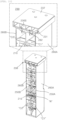
- FIGS. 8A and 8B are exploded perspective views for describing a coupling relation of the radiation element part, among the components of the RF module for an antenna, with the unit RF filter body.
- FIG. 9 is a cutaway perspective view and a partially enlarged view illustrating a form of a mutual electrical connection by a third connection pin terminal illustrated in FIGS. 8A and 8B .
- At least one input and output port 287 for transferring a transmission signal through the left filter part 240A and the right filter part 240B may be provided on the rear surface side of the unit RF filter body 210.
- the main board 120, the left filter part 240A, and the right filter part 240B may be electrically connected to the at least one input and output port 287 through the medium of the first connection pin terminal 281.
- the base panel 221 of the radiation element part 220 may be electrically connected by at least one third connection pin terminal 283 in order to mediate the transfer of a transmission signal from each of the left filter part 240A and the right filter part 240B and a reception signal from the director panel 225 for radiation.
- the third connection pin terminal 283 may be soldered and fixed to the base panel 221 by using a coupling method, such as soldering, after being coupled in a terminal pin coupling way.
- each of the left filter part 240A and the right filter part 240B and the radiation element parts 220 in front thereof may be electrically connected through the reflector panel 270.
- a pair of pin terminal installation holes 271 that are penetrated in forward and backward directions may be formed in the front surface of the unit RF filter body 210 that forms the reflector panel 270.
- the third connection pin terminal 283 may be penetrated and installed through the pair of pin terminal installation holes 271.
- the pair of pin terminal installation holes 271 may be provided to have a number in which the pin terminal installation holes are electrically connected to the cavity C1 of the left filter part 240A and the cavity C2 of the right filter part 240B.
- the at least one third connection pin terminal 283 has an advantage in that an error (the non-linearity of contraction resistance) of a metal contact point can be reduced because one end of the base panel 221 is soldered and fixed to the base panel 221 in order to improve the PIM problem.
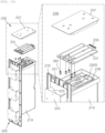
- FIG. 10 is an exploded perspective view for describing a coupling relation of an amplification element part with the unit RF filter body, among the components of the RF module for an antenna.
- FIG. 11 is a cutaway perspective view and a partially enlarged view illustrating a form of a mutual electrical connection by a second connection pin terminal illustrated in FIG. 10 .
- the LNA board part 231 on which at least one LNA element has been mounted may be accommodated and disposed on the board installation space 230S that is integrally formed on any one of the upper surface and lower surface of the unit RF filter body 210.
- a penetration slit 239 that is penetrated toward the rear side of the unit RF filter body 210 may be formed in the board installation space 230S.
- the male socket part 235 formed in the LNA board part 231 may be penetrated and coupled to the female socket part 125 provided in the main board 120 in a socket pin coupling way through the penetration slit 239 so that a reception signal can be electrically connected.
- At least one LNA element that performs a function for amplifying the reception signal received via the left filter part 240A or the right filter part 240B from the radiation element part 220, among analog amplification elements, may be mounted on the LNA board part 231.
- At least one PA (Tx-amp) element except the LNA element mounted on the LNA board part 231 may be mounted on the main board 120.
- the PA elements mounted on the main board 120 can widen an interval between heat-generation elements mounted on the main board 120 because the LNA elements are distributed, disposed, and designed on the side of the RF module 200 separated from the main board 120 in that the amount of heat generation from the PA elements is relatively much greater than that of the LNA elements. Accordingly, overall heat dissipation performance can be improved because heat generated by the heat-generation elements can be prevented from being concentrated.
- the LNA board part 231 may be electrically connected to the cavities C1 and C2 of the left filter part 240A and the right filter part 240B formed on the left and right sides of the unit RF filter body 210, respectively, through the medium of the at least one second connection pin terminal 282.
- a pin installation hole (a reference numeral not indicated) that penetrates the board installation space 230S, the cavity C1 of the left filter part 240A, and the cavity C2 of the right filter part 240B may be formed in the unit RF filter body 210.
- the second connection pin terminal 282 may be soldered and fixed to the LNA board part 231 by a coupling method, such as soldering.
- one end of the at least one second connection pin terminal 282, which is close to the LNA board part 231, may be soldered and fixed to the LNA board part 231 in order to improve the PIM problem.
- the RF module 200 for an antenna has advantages in that it can maintain the PIM characteristic by improving movement and spacing problems of embedded parts, which may occur due to a weak coupling force for the main board 120 by the first connection pin terminal 281 and the male socket part 235 of the LNA board part 231, and can also maintain a stable PIM characteristic by soldering and fixing the first connection pin terminal 281, the second connection pin terminal 282, and the third connection pin terminal 283.
- the RF module 200 for an antenna may further include a left tuning cover 250A and a right tuning cover 250B coupled to cover the cavities C1 and C2 on the left and right sides of the unit RF filter body 210, respectively, and a left filter cover 260A and a right filter cover 260B that shield the left tuning cover 250A and the right tuning cover 250B.
- Tuning grooves 251 may be formed in the left tuning cover 250A and the right tuning cover 250B so that precise frequency tuning is performed through the adjustment of a distance from the resonator R within each of the cavities C1 and C2.
- the frequency filtering process within each of the cavities C1 and C2 of the unit RF filter body 210 needs to be performed in the state in which each cavity has been fully sealed. If the sealing is not complete or sealing performance is reduced due to an increase of a use period, there is room for the occurrence of the PIM problem.
- the left filter cover 260A and the right filter cover 260B including the left tuning cover 250A and the right tuning cover 250B may be attached to the unit RF filter body 210 in a laser welding way.
- the antenna apparatus 100 may be a concept that fully includes the RF module 200 for an antenna.
- the antenna apparatus 100 includes the antenna housing part 110 formed in the form of an enclosure having a front surface opened, the main board 120 that is stacked and disposed to be closely attached to the inside of the antenna housing part 110, and the multiple RF modules 200 for an antenna, which are arranged on the front surface of the main board 120.
- the multiple RF modules 200 for an antenna each include the unit RF filter body 210 arranged on the front surface of the main board 120, the radiation element part 220 disposed on the front surface of the unit RF filter body 210, the amplification element part 230 provided on any one of the upper surface and the lower surface, that is, the front and rear thickness parts of the unit RF filter body 210, and including the LNA board part 231 on which at least one analog amplification element has been mounted, and the reflector panel 270 that is formed to extend wider than the area of the front surface of the unit RF filter body 210 in a front cross section of the unit RF filter body 210 and that grounds (GND) the radiation element part 220.
- the unit RF filter body 210 arranged on the front surface of the main board 120
- the radiation element part 220 disposed on the front surface of the unit RF filter body 210
- the amplification element part 230 provided on any one of the upper surface and the lower surface, that is, the front and rear thickness parts of the unit
- the multiple cavities C1 and C2 each opened to the outside on the left and right sides thereof are formed on the left and right sides of the unit RF filter body 210.
- the left filter part 240A and the right filter part 240B in each of which the resonator R is embedded and which each perform different frequency filtering are provided in the cavities C1 and C2, respectively.
- the present disclosure provides the RF module for an antenna, which is capable of a heat distribution by separating the LNA board part on which an LNA element having a slightly small amount of heat generation, among heat-generation elements, has been mounted from the main board and coupling the LNA board part to the unit RF filter body side, which can improve the productivity of a product by modulating the radiation element part, the left filter part, the right filter part, and the amplification element part so that the radiation element part, the left filter part, the right filter part, and the amplification element part can be manufactured in a module unit and assembled on at least any one of a front surface, left and right sides, and upper and lower surfaces of the RF filter body, and can stably fix and support the RF module for an antenna, which has been manufactured in a modularization unit so that the PIM characteristic can be maintained, and the antenna apparatus including the same.
Landscapes
- Physics & Mathematics (AREA)
- Electromagnetism (AREA)
- Engineering & Computer Science (AREA)
- Computer Networks & Wireless Communication (AREA)
- Variable-Direction Aerials And Aerial Arrays (AREA)
- Aerials With Secondary Devices (AREA)
- Support Of Aerials (AREA)
Abstract
Description
- The present disclosure relates to an RF module for an antenna and an antenna apparatus including the same, and more particularly, to an RF module for an antenna, an RF module assembly, and an antenna apparatus including the same, wherein a radiation element module and an RF element are fully separated from a main board, but are disposed to be exposed to an ambient air ahead thereof and which can solve a difficulty in a heat dissipation design toward on the front side thereof having a conventional radiation element.
- A base station antenna including a relay that is used in a mobile communication system has various forms and structures. In general, the base station antenna has a structure in which multiple radiation elements are properly disposed on at least one reflection plate that stands upright in a length direction thereof.
- Recently, research is actively attempted to achieve a small-sized, lightweight, and low-cost structure while satisfying high performance requirements for a multi-input & multi-output (MIMO)-based antenna. In particular, in the case of an antenna apparatus to which a radiation element having a patch type and for implementing linear polarization or circular polarization has been applied, in general, a method of plating a radiation element consisting of a dielectric board made of a plastic or ceramic material and coupling the radiating element to a printed circuit board (PCB) through soldering is widely used.
-
FIG. 1 is an exploded perspective view of illustrating an example of an antenna apparatus according to a conventional technology. - As illustrated in
FIG. 1 , in anantenna apparatus 1 according to the conventional technology,multiple radiation elements 35 are arranged on the front side of anantenna housing body 10, that is, a beam output direction, so that beams are output in a desired direction to facilitate beamforming. In order to protect the radiation elements against an external environment, aradome 50 is mounted at the front end of theantenna housing body 10 with themultiple radiation elements 35 interposed therebetween. - More specifically, the
antenna apparatus 1 according to the conventional technology is provided in the form of a thin rectangular parallelepiped enclosure having a front opened, and includes theantenna housing body 10 in which multipleheat dissipation pins 11 have been integrally formed, amain board 20 that is stacked and disposed on a rear surface of theantenna housing body 10 therein, and anantenna board 30 that is stacked and disposed on a front surface of theantenna housing body 10 therein, at the rear of the enclosure. - The patch type radiation elements or dipole
type radiation elements 35 may be mounted on a front surface of theantenna board 30. Theradome 50 that enables radiation from theradiation elements 35 to be smoothly performed, while protecting parts therein against the outside, may be installed in front of theantenna housing body 10. - However, the example 1 of the antenna apparatus according to the conventional technology has a structure in which various digital elements (an FPGA element, etc.) and analog amplification elements (a PA element, an LNA element, etc.) are intensively mounted on the
main board 20 so that heat is dissipated toward the back of theantenna housing body 10. - In this case, the LNA element, among the analog amplification elements, has problems in that it increases the density of installation distributions for the main board of other heat-generation elements and has a cause to directly degrade performance due to the generation of heat from other heat-generation elements because the LNA element has a small amount of heat generation and is also mounted on the
main board 20. - Furthermore, a common antenna apparatus has a passive inter-modulation (PIM) problem. PIM is a spurious signal that is generated due to a non-linear characteristic of a passive element, and refers to a phenomenon in which the spurious signal deteriorates communication quality by reducing a signal to noise characteristic on a communication path.
- The PIM characteristic within equipment of a distributed antenna system (DAS) is maintained with predetermined quality or higher upon production, but may have a PIM problem due to a passive element that is used in a distribution network up to the final antenna at the rear end of an antenna port of remote equipment in the field.
- In particular, if an antenna apparatus is designed to have a structure in which internal parts, such as an antenna element, are modulated and mounted, the PIM problem becomes great compared to the integrated mounting case if the modules are not stably fixed.
- The present disclosure has been intended to solve the aforementioned technical problems, and an object of the present disclosure is to provide an RF module for an antenna, which is capable of a heat distribution by separating an LNA board part on which an LNA element having a slightly small amount of heat generation, among heat-generation elements, has been mounted from a main board and coupling the LNA board part to the unit RF filter body side, and an antenna apparatus including the same.
- Furthermore, another object of the present disclosure is to provide an RF module for an antenna, which can improve the productivity of a product by modulating a radiation element part, a left filter part, a right filter part, and an amplification element part so that the radiation element part, the left filter part, the right filter part, and the amplification element part can be manufactured in a module unit and assembled on at least any one of front surface, left and right sides, and upper and lower surfaces of an RF filter body, and an antenna apparatus including the same.
- Furthermore, still another object of the present disclosure is to provide an antenna apparatus capable of stably fixing and supporting an RF module for an antenna which is manufactured in a modulation unit so that the PIM characteristic can be maintained.
- Technical objects of the present disclosure are not limited to the aforementioned objects, and the other objects not described above may be evidently understood from the following description by those skilled in the art.
- An embodiment of an RF module for an antenna according to the present disclosure includes a unit RF filter body arranged on a front surface of a main board, a radiation element part disposed on a front surface of the unit RF filter body, and a reflector panel configured to form the front surface of the unit RF filter body, formed to be wider than the area of a vertical cross section of the unit RF filter body, and configured to ground (GND) the radiation element part. A left filter part and a right filter part in which multiple cavities each opened to the outside on left and right sides thereof have been formed and which each have a resonator embedded in each cavity and perform different frequency filtering are provided on left and right sides of the unit RF filter body, respectively. The left filter part and the right filter part are electrically connected to the radiation element part through the reflector panel.
- In this case, a pair of pin terminal installation holes through which a third connection pin terminal configured to mediate the transfer of transmission signals and reception signal of the left filter part, the right filter part, and the radiation element part is installed may be formed in the reflector panel.
- Furthermore, the radiation element part may be provided to generate one polarization, among at least two multi-polarizations.
- Furthermore, the radiation element part includes a base panel disposed on a front surface of the reflector panel, a power feeding base attached to the base panel and electrically connected to the left filter part and the right filter part, and a director panel for radiation which is provided at a front end of the power feeding base.
- Furthermore, the third connection pin terminal may be soldered and fixed to the base panel.
- Furthermore, the RF module may further include an amplification element part including an LNA board part that is provided on any one of an upper surface and lower surface that are front and rear thickness parts of the unit RF filter body and on which at least one analog amplification element has been mounted.
- Furthermore, in the amplification element part, an LNA board part may be disposed in a board installation space provided on an upper surface or a lower surface that forms a front and rear thickness part of the unit RF filter body. The LNA board part may be electrically connected to each of the cavities of the left filter part and right filter part formed on the left and right sides of the unit RF filter body.
- Furthermore, a male socket part to be coupled in a socket pin coupling way with respect to the main board may be formed in the LNA board part. A penetration slit through which the male socket part of the LNA board part passes may be formed in a board installation space.
- Furthermore, at least one LNA element configured to amplify a reception signal that is received via the left filter part or the right filter part from the radiation element part may be mounted on the LNA board part. At least one PA element except the LNA element may be mounted on the main board. Heat generated from the at least one PA element may be discharged to the back of an antenna housing on which the main board has been stacked.
- Furthermore, a pin installation hole that penetrates through the board installation space, the cavity of the left filter part, and the cavity of the right filter part may be formed in the unit RF filter body. The LNA board part, the left filter part, and the right filter part may be electrically connected by at least one second connection pin terminal installed in each pin installation hole. The second connection pin terminal may be soldered and fixed to the LNA board part.
- Furthermore, at least one input and output port for transferring transmission signals through the left filter part and the right filter part may be provided in the unit RF filter body. The main board, the left filter part, and the right filter part may be electrically connected to the at least one input and output port through a medium of the at least one first connection pin terminal.
- Furthermore, the at least one first connection pin terminal may be soldered and fixed to the front surface of the main board
- An antenna apparatus including an RF module for an antenna according to an embodiment of the present disclosure includes an antenna housing part formed in a form of an enclosure having a front surface opened, a main board stacked and disposed to be closely attached to an inside of the antenna housing part, and multiple RF modules for an antenna, which are arranged on a front surface of the main board. The multiple RF modules for an antenna may include a unit RF filter body arranged on the front surface of the main board, a radiation element part disposed on a front surface of the unit RF filter body, and a reflector panel configured to form the front surface of the unit RF filter body, formed to be wider than the area of a vertical cross section of the unit RF filter body, and configured to ground (GND) the radiation element part. A left filter part and a right filter part in which multiple cavities each opened to the outside on left and right sides thereof have been formed and which each have a resonator embedded in each cavity and perform different frequency filtering may be provided on left and right sides of the unit RF filter body, respectively. The left filter part and the right filter part may be electrically connected to the radiation element part through the reflector panel.
- In this case, the multiple RF modules for an antenna may each further include an amplification element part including an LNA board part that is provided on any one of an upper surface and lower surface that are front and rear thickness parts of the unit RF filter body and on which at least one analog amplification element has been mounted.
- Furthermore, the radiation element part may include a base panel disposed on a front surface of the reflector panel. The left filter part and the right filter part may be soldered and fixed to the main board so that the left filter part and the right filter part are electrically connected to the main board through a medium of at least one first connection pin terminal. The left filter part and the right filter part may be soldered and fixed to an LNA board part so that the left filter part and the right filter part are electrically connected to the LNA board part through a medium of at least one second connection pin terminal. The left filter part and the right filter part may be soldered and fixed to the base panel so that the left filter part and the right filter part are electrically connected to the base panel through a medium of at least one third connection pin terminal.
- Furthermore, the antenna apparatus may further include a fixing member having both left and right ends fixed to left and right side walls of the antenna housing part and configured to fix the unit RF filter body. The fixing member may be made of a non-conductive material.
- According to an embodiment of the RF module for an antenna and the antenna apparatus including the same according to the present disclosure, the following various effects can be achieved.
- First, there is an effect in that overall heat dissipation performance can be improved because the LNA element provided on a reception signal path, which has a relatively small amount of heat generation, among heat-generation elements of the antenna apparatus, and does not affect the entire system, is disposed to be separated from the main board.
- Second, there is an effect in that the productivity of a dual band filter can be improved because the left filter part and the right filter part capable of performing mutual and independent frequency filtering are provided on the left and right of the unit RF filter body, respectively.
- Third, there is an effect in that a common PIM characteristic of the antenna apparatus can be maintained because the filter part, the radiation element part, and the amplification part are manufactured in one module unit and assembled, and the main board, the filter part, the amplification part, and the filter part, and the filter part and the radiation element part are electrically connected through the medium of the connection pin terminals and are provided to be soldered and fixed, and the fixing member is further provided.
- Effects of the present disclosure are not limited to the aforementioned effects, and the other effects not described above may be evidently understood by those skilled in the art from the writing of the claims.
-
-
FIG. 1 is an exploded perspective view illustrating an example of an antenna apparatus according to a conventional technology. -
FIG. 2 is a perspective view illustrating an antenna apparatus according to an embodiment of the present disclosure. -
FIG. 3 is a general exploded perspective view ofFIG. 2 . -
FIG. 4 is an exploded perspective view for describing a process of installing a main board of an RF module for an antenna, among components ofFIG. 2 . -
FIG. 5 is an exploded perspective view for describing a process of installing a fixing member, among the components ofFIG. 2 . -
FIGS. 6A and6B are perspective views illustrating a front part and rear part of the RF module for an antenna, among the components ofFIG. 2 . -
FIGS. 7A to 7D are exploded perspective views in a left direction and right direction ofFIGS. 6A and6B . -
FIGS. 8A and8B are exploded perspective views for describing a coupling relation of a radiation element part, among the components of the RF module for an antenna, with a unit RF filter body. -
FIG. 9 is a cutaway perspective view and a partially enlarged view illustrating a form of a mutual electrical connection by a third connection pin terminal illustrated inFIGS. 8A and8B . -
FIG. 10 is an exploded perspective view for describing a coupling relation of an amplification element part with the unit RF filter body, among the components of the RF module for an antenna. -
FIG. 11 is a cutaway perspective view and a partially enlarged view illustrating a form of a mutual electrical connection by a second connection pin terminal illustrated inFIG. 10 . -
100: antenna apparatus 110: antenna housing part 110S: internal space 111: rear heat dissipation pin 120: main board 125: female socket part 130: PSU board part 140: RFIC board part 150: surge board part 200: RF module for an antenna 210: unit RF filter body 220: radiation element part 230: amplification element part 270: reflector panel 287: input and output port - Hereinafter, an RF module for an antenna and an antenna apparatus including the same according to an embodiment of the present disclosure are described in detail with reference to the accompanying drawings.
- In adding reference numerals to the components of each drawing, it should be noted that the same components have the same reference numerals as much as possible even if they are displayed in different drawings. Furthermore, in describing embodiments of the present disclosure, when it is determined that a detailed description of the related well-known configuration or function hinders understanding of an embodiment of the present disclosure, the detailed description thereof will be omitted.
- Furthermore, in describing components of an embodiment of the present disclosure, terms, such as a first, a second, A, B, (a), and (b), may be used. Such terms are used only to distinguish one component from another component, and the essence, order, or sequence of a corresponding component is not limited by the terms. All terms used herein, including technical or scientific terms, have the same meanings as those commonly understood by a person having ordinary knowledge in the art to which the present disclosure pertains, unless defined otherwise in the specification. Terms, such as those commonly used and defined in dictionaries, should be construed as having the same meanings as those in the context of a related technology, and are not construed as having ideal or excessively formal meanings unless explicitly defined otherwise in the specification.
-
FIG. 2 is a perspective view illustrating an antenna apparatus according to an embodiment of the present disclosure.FIG. 3 is a general exploded perspective view ofFIG. 2 .FIG. 4 is an exploded perspective view for describing a process of installing a main board of an RF module for an antenna, among the components ofFIG. 2 .FIG. 5 is an exploded perspective view for describing a process of installing a fixing member, among the components ofFIG. 2 . - As referred in
FIGS. 2 to 5 , anantenna apparatus 100 according to an embodiment of the present disclosure includes anantenna housing part 110 that forms external appearances of left and right sides and rear side of theantenna apparatus 100, and aradome panel 300 that forms an external appearance of the front of theantenna apparatus 100, that is provided to shield an opened front surface of theantenna housing part 110, and that protects internal parts (including amain board 120 and anRF module 200 for an antenna described later) provided in aninternal space 110S of theantenna housing part 110 against the outside. - Furthermore, as referred in
FIGS. 2 to 5 , theantenna apparatus 100 according to an embodiment of the present disclosure further includes themain board 120 closely installed in theinternal space 110S of theantenna housing part 110, aPSU board part 130 disposed on an upper side of themain board 120, anRFIC board part 140 provided between the pair ofmain boards 120, and asurge board part 150 at a lower part of themain board 120, and may further include the radio frequency module 200 (hereinafter abbreviated as the "RF module") for an antenna that is stacked and disposed a front surface of themain board 120. - Although not illustrated, the
antenna housing part 110 may play a role of mediating the coupling of a pillar pole that is provided to install theantenna apparatus 100. - The
antenna housing part 110 is generally provided as a metal material having excellent thermal conductivity in order to be advantageous for heat dissipation according to thermal conduction, and may be formed in the form of a rectangular enclosure having a thickness in forward and backward directions to the extent that the front end of theRF module 200 described later can be accommodated therein. - Meanwhile, the inside of the
antenna housing part 110 may be formed in a form in which the inside of the antenna housing part is matched with an external protrusion shape by a digital element (an FPGA element, etc.) mounted on a rear surface of themain board 120 and/or a PSU element mounted on a rear surface of thePSU board part 130 and surge part elements mounted on a rear surface of thesurge board part 150. This is for maximizing heat dissipation performance by increasing a thermal contact area with the rear surfaces of themain board 120, thePSU board part 130, and thesurge board part 150 as much as possible. - Furthermore, a
female socket part 125 to which amale socket part 235 formed in anLNA board part 231 of anamplification element part 230, among components of theRF module 200 for an antenna, which are manufactured in a module unit described later, is coupled in a socket pin coupling way may be provided on the front surface of themain board 120, and apin coupling part 123 to which firstconnection pin terminals 281 of aleft filter part 240A and aright filter part 240B, among components of theRF module 200 for an antenna, is coupled in a terminal pin coupling way may be provided on the front surface of the main board. - Although not illustrated in the drawings, handle parts which may be held by a worker so that the worker can carry the
antenna apparatus 100 according to an embodiment of the present disclosure or can easily mount a pillar pole (not illustrated) manually on the spot may be further installed on both left and right sides of theantenna housing part 110. - Furthermore, various outside mounting
members 400 for a cable connection with a base station apparatus not illustrated and the tuning of internal parts may be assembled with the outside of the bottom of theantenna housing part 110 through the antenna housing part. Theoutside mounting members 400 are provided in the form of at least one optical cable connection terminal (socket). Connection terminals of coaxial cables (not illustrated) may be mutually connected to connection terminals of the outside mounting members, respectively. - Referring to
FIGS. 2 to 5 , multiple rear heat dissipation pins 111 may be integrally formed on a rear surface of theantenna housing part 110 so that the multiple rear heat dissipation pins have a predetermined pattern shape. However, the multiple rear heat dissipation pins 111 do not need to be essentially integrally formed on the rear surface of theantenna housing part 110. It may be said to be natural that the multiple rear heat dissipation pins may be manufactured as individual parts and may be coupled to the rear surface of theantenna housing part 110 in various coupling ways including a laser welding method. - In this case, heat that is generated from each of heat-generation elements of the
main board 120, thePSU board 130, theRFIC board part 140, and thesurge board part 150 installed in theinternal space 110S of theantenna housing part 110 may be directly discharged backward through the multiple rear heat dissipation pins 111. - As referred in
FIGS. 2 to 5 , the multiple rear heat dissipation pins 111 are upward slantly disposed toward a left end and a right end thereof on the basis of an upper and lower portion that connects the middle of a left and right width thereof, and may be designed so that pieces of heat that are discharged to the back of theantenna housing part 110 form an upcurrent distributed in the horizontal direction and are distributed more rapidly. However, a shape of the multiple rear heat dissipation pins 111 is not essentially limited thereto. For example, although not illustrated in the drawings, if a blower fan module (not illustrated) is further provided on the rear surface side of theantenna housing part 110 in order to make smooth a flow of an ambient air, the multiple rear heat dissipation pins 111 may be adopted so that the multiple rear heat dissipation pins are formed in parallel at the left end and the right end in the blower fan module that is disposed at the center thereof in order for discharged heat to be discharged more rapidly by the blower fan module. - Meanwhile, the
radome panel 300 is coupled to a front end of theantenna housing part 110, but ahook coupling part 310 that is formed along the edge of theradome panel 300 may be hook-coupled to the front locking rib (a reference numeral not indicated) side of theantenna housing part 110. - In this case, a
waterproof gasket ring 180 made of a rubber material may be interposed between the edge of the front end of theantenna housing part 110 and theradome panel 300. Thewaterproof gasket ring 180 may perform a sealing function while being elastically deformed by a coupling force that is provided upon hook-coupling with theantenna housing part 110 of theradome panel 300. - Meanwhile, as referred in
FIGS. 3 to 5 , theantenna apparatus 100 according to an embodiment of the present disclosure may further include fixingmembers 280 for fixing a unitRF filter body 210 of eachRF module 200 upon installation of theRF module 200 for an antenna. - As referred in
FIG. 5 , the fixingmember 280 may be fixed as both left and right ends of the fixing member are disposed within multiple left and right penetration holes 171 provided to penetrate left and right side walls of theantenna housing part 110 and multiple assembly screws 173 are fastened to screw fastening holes 281 formed at both left and right ends of the fixing member through the multiple left and right penetration holes 171 from the outside. - The multiple left and right penetration holes 171 formed in the
antenna housing part 110 and the multiple assembly screws 173 fastened to the multiple left and right penetration holes may have a danger of damaging a fine sight due to exposure to the outside. Accordingly, as referred inFIGS. 2 to 5 , each of the multiple left and right penetration holes 171 may be shielded from the outside by attaching aseparate shielding film 175 thereto. - Furthermore, multiple module fixing
screw holes 283 may be formed in the fixingmember 280 so that the multiple module fixing screw holes are horizontally spaced apart from each other. Multiple assembly screws (not illustrated) may be fastened to module fixing screw fastening holes 275 formed in areflector panel 270, among components of theRF module 200 assembled in theinternal space 110S of theantenna housing part 110. Accordingly, eachRF module 200 can be stably fixed. - As multiband operation base stations having increased frequency bands are recently increased, a passive inter-modulation (PIM) phenomenon is recognized as a very big problem by a communication service provider.
- The PIM phenomenon is a phenomenon that occurs due to a kind of radio wave interference, and major causes thereof include radio waves of several frequencies and rusty metal, in general. However, the PIM phenomenon is not a problem that essentially occurs by the two factors only. For example, as the
antenna housing part 110 is lengthily formed vertically due to the application of the multi-input & multi-output (MIMO) technology, the non-linearity (an error of a metal contact point) of contraction resistance that is generated between electrical connection elements due to a fine twist attributable to the skewed and concentrated heat generation of heat-generation elements that operate for an operation of the antenna housing part may become a cause of the PIM problem. - In this case, it is preferred that a non-conductive material (e.g., a plastic resin-based material) is adopted as the fixing
member 280 so that the PIM influence is minimized and the influence of thereflector panel 270 described later on a ground (GND) role is minimized. It is preferred that a plastic resin-based material is also adopted as the multiple assembly screws (not illustrated). - Furthermore, the
antenna apparatus 100 according to an embodiment of the present disclosure, although not illustrated in the drawings, may further include a buffering part made of a silicon rubber material, which is attached to a front end of the fixingmember 280. The buffering part may play a role of reducing an internal impact between parts by being seated and installed in the fixingmember 280 that fixes each unitRF filter body 210. - It is difficult to maintain the PIM characteristic in that each RF module is modulated and manufactured as described above and a coupling force between the
main board 110 and eachRF module 200 depends on a very weak coupling force between themale socket part 235 of theLNA board part 231 and the firstconnection pin terminals 281 of the RFfilter body part 210 as described later. Accordingly, the PIM problem may be solved by using the fixingmember 280 that firmly fixes and supports eachRF module 200. This is described later while describing each component of theRF module 200 in detail. -
FIGS. 6A and6B are perspective views illustrating a front part and rear part of the RF module for an antenna, among the components ofFIG. 2 .FIGS. 7A to 7D are exploded perspective views in the left direction and right direction ofFIGS. 6A and6B . - Referring to
FIGS. 6A to 7D , an embodiment of theRF module 200 for an antenna according to the present disclosure may include the unitRF filter body 210 arranged on the front surface of themain board 120, aradiation element part 220 disposed on a front surface of the unitRF filter body 210, and thereflector panel 270 that forms the front surface of the unitRF filter body 210, that is formed to be wider than the area of a vertical cross section of the unitRF filter body 210, and that grounds (GND) theradiation element part 220. - In this case, multiple cavities C1 and C2 that have been opened to the outside on the left and right sides thereof are formed on the left and right sides of the unit
RF filter body 210, respectively. Theleft filter part 240A and theright filter part 240B each having a resonator R embedded therein and performing different frequency filtering may be provided within the cavities C1 and C2, respectively. Hereinafter, theleft filter part 240A and theright filter part 240B are described by defining that the left filter part and the right filter part are disposed on the left and right sides on the basis of a front direction. - Furthermore, the resonator R may be a resonator having a bar shape, but a shape thereof is not limited thereto. The resonator may also be made of various materials, such as dielectrics such as ceramic, or metal.
- The
left filter part 240A and theright filter part 240B may be designed as filters for a frequency band of 2.4G and a frequency band of 5G, respectively, and may implement a dual band antenna by oneRF module 200. - Meanwhile, the
radiation element part 220 may be provided to generate two or more multiple polarizations. Hereinafter, theradiation element part 220 that has implemented dual polarization, among multiple polarizations, is described in detail as an example. - As referred in
FIGS. 6A to 7D , the RF module may includebase panels 221 each disposed on a front surface of thereflector panel 270, power feeding bases 223 attached to thebase panels 221, electrically connected to theleft filter part 240A and theright filter part 240B, and each intersected and arranged in an "X" shape, anddirector panels 225 for radiation, which are provided at a front end of thepower feeding base 223. In an embodiment of the present disclosure, thepower feeding base 223 has been limited to being intersected and arranged in the "X" shape with respect to thebase panel 221, but the present disclosure is not essentially thereto and does not exclude the array of the power feeding base in a "" shape, an "H" shape, and a "+" shape.
- The
director panel 225 for radiation is formed in an approximately square shape. Thepower feeding base 223 is disposed to diagonally support each edge portion of thedirector panel 225 for radiation, and each feeding end thereof is extended to be disposed at a central part of each side of thedirector panel 225 for radiation and fed and connected. Accordingly, eachpower feeding base 223 may implement dual polarization by generating each polarization. - The
base panels 221 may be electrically connected to mediate the transfer of transmission signals from theleft filter part 240A and theright filter part 240B formed on the left and right sides of the unitRF filter body 210, respectively, and the transfer of a reception signal from thedirector panel 225 for radiation. An electrical connection mechanism between thebase panel 221 and each of thefilter parts - In the
RF module 200 for an antenna according to an embodiment of the present disclosure, theradiation element part 220 is limited to being described as any one of the patch type and the dipole type, but the present disclosure is not essentially limited thereto. It is to be noted that the application of an air strip type antenna is not excluded. - Meanwhile, as referred in
FIGS. 6A to 7D , theRF module 200 for an antenna according to an embodiment of the present disclosure may further include theamplification element part 230 including theLNA board part 231 that is provided on any one of an upper surface and a lower surface, that is, front and rear thickness parts of the unitRF filter body 210, and on which at least one analog amplification element (not illustrated) has been mounted. - Meanwhile, as referred in
FIGS. 6A to 7D , theamplification element part 230 may include theLNA board part 231 in aboard installation space 230S that is provided on any one of the upper surface and the lower surface that form the front and rear thickness parts of the unitRF filter body 210. - At least one LNA element (not illustrated) having a relatively small amount of heat generation, among analog amplification elements, and playing a role of amplifying a reception signal may be mounted on the
LNA board part 231. - In general, an RF module is an array of analog RF parts. For example, analog amplification elements that amplify an RF signal are mounted on the
amplification element part 230. In the case of theRF module 200 according to an embodiment of the present disclosure, only LNA elements having relatively small heat generation, among analog amplification elements, have been separated from themain board 120 and designed to be included in the unitRF filter body 210. Furthermore, theleft filter part 240A and theright filter part 240B are each an RF part for frequency-filtering an input RF signal into a desired frequency band. Theradiation element part 220 may be defined as an RF part that plays a role of receiving and transmitting RF signals. - In this case, the
LNA board part 231 may be electrically connected to the cavities C1 and C2 of theleft filter part 240A and theright filter part 240B that are formed on the left and right sides of the unitRF filter body 210, respectively. An electrical connection mechanism between theLNA board part 231 and each of thefilter parts - The
board installation space 230S in which theLNA board part 231 has been installed may be shielded by using an amplificationpart cover panel 237. An amplification part heat sink pin (not illustrated) that discharges heat within theboard installation space 230S in a thermal conduction way may be integrally formed on an outside surface of the amplificationpart cover panel 237. The heat that is discharged through the amplification part heat sink pin may be discharged to the outside through a lateral part of theantenna housing part 110. - An embodiment in which only the LNA elements, among multiple analog amplification elements mounted and disposed in the existing
main board 120 on the side of the unitRF filter body 210, are separately separated and provided as theamplification element part 230 as described above may be defined as components that perform a great role in the improvement of the PIM problem. - That is, the reason for this is that if the LNA elements are mounted on the
main board 120 along with other heat-generation elements without being separated from themain board 120, a mounting interval for multiple analog amplification elements becomes inevitably narrow and when operation heat from such multiple analog amplification elements is generated, there is a great danger of a twist phenomenon which occurs due to the thermal skew of theantenna housing part 110 that is lengthily formed vertically. - However, the
amplification element part 230 does not need to be essentially included in the unitRF filter body 210. According to an embodiment, it may be said to be natural that theamplification element part 230 may not be separated from the existingmain board 120 or may be implemented to be not included in the unitRF filter body 210 although theamplification element part 230 is separated. - Meanwhile, as referred in
FIGS. 6A to 7D , thereflector panel 270 may be formed on the front surface of the unitRF filter body 210. - The
reflector panel 270 may play a role of preventing a radio wave (beam), which is radiated by theradiation element part 220 coupled to a front end of the unitRF filter body 210, from infiltrating into the rear side thereof and serves as a ground (GND) for theradiation element part 220. - Furthermore, the module fixing screw fastening holes 275 to which the multiple assembly screws (not illustrated) for screw fixing by the fixing
member 280 described with reference toFIGS. 2 to 5 are fastened may be formed at an upper end part and lower end part of thereflector panel 270. - As already described, the fixing
member 280 is for supplementing a weak coupling force of the unitRF filter body 210 for themain board 120, and can improve the PIM problem attributable to a movement or spacing of the unitRF filter body 210 by stably fixing each unitRF filter body 210 in front thereof in a process of the fixing members being assembled with internal walls of theinternal space 110S of theantenna housing part 110 on the left and right sides thereof. -
FIGS. 8A and8B are exploded perspective views for describing a coupling relation of the radiation element part, among the components of the RF module for an antenna, with the unit RF filter body.FIG. 9 is a cutaway perspective view and a partially enlarged view illustrating a form of a mutual electrical connection by a third connection pin terminal illustrated inFIGS. 8A and8B . - As referred in
FIGS. 8A and8B , theleft filter part 240A and theright filter part 240B formed on the left and right sides of the unitRF filter body 210, respectively, may be electrically connected through the medium of the at least one firstconnection pin terminal 281 that is included in thepin coupling part 123 provided on the front surface of themain board 120. - More specifically, at least one input and
output port 287 for transferring a transmission signal through theleft filter part 240A and theright filter part 240B may be provided on the rear surface side of the unitRF filter body 210. - In this case, the
main board 120, theleft filter part 240A, and theright filter part 240B may be electrically connected to the at least one input andoutput port 287 through the medium of the firstconnection pin terminal 281. - In this case, a rear end part of the at least one first
connection pin terminal 281 may be soldered and fixed to the front surface of themain board 120 in order to improve the PIM problem. - Meanwhile, referring to
FIGS. 7A and7B , thebase panel 221 of theradiation element part 220 may be electrically connected by at least one thirdconnection pin terminal 283 in order to mediate the transfer of a transmission signal from each of theleft filter part 240A and theright filter part 240B and a reception signal from thedirector panel 225 for radiation. - In this case, the third
connection pin terminal 283 may be soldered and fixed to thebase panel 221 by using a coupling method, such as soldering, after being coupled in a terminal pin coupling way. - More specifically, each of the
left filter part 240A and theright filter part 240B and theradiation element parts 220 in front thereof may be electrically connected through thereflector panel 270. - To this end, a pair of pin terminal installation holes 271 that are penetrated in forward and backward directions may be formed in the front surface of the unit
RF filter body 210 that forms thereflector panel 270. The thirdconnection pin terminal 283 may be penetrated and installed through the pair of pin terminal installation holes 271. - The pair of pin terminal installation holes 271 may be provided to have a number in which the pin terminal installation holes are electrically connected to the cavity C1 of the
left filter part 240A and the cavity C2 of theright filter part 240B. - In particular, the at least one third
connection pin terminal 283 has an advantage in that an error (the non-linearity of contraction resistance) of a metal contact point can be reduced because one end of thebase panel 221 is soldered and fixed to thebase panel 221 in order to improve the PIM problem. -
FIG. 10 is an exploded perspective view for describing a coupling relation of an amplification element part with the unit RF filter body, among the components of the RF module for an antenna.FIG. 11 is a cutaway perspective view and a partially enlarged view illustrating a form of a mutual electrical connection by a second connection pin terminal illustrated inFIG. 10 . - As referred in
FIGS. 10 and11 , in theamplification element part 230, theLNA board part 231 on which at least one LNA element has been mounted may be accommodated and disposed on theboard installation space 230S that is integrally formed on any one of the upper surface and lower surface of the unitRF filter body 210. - A penetration slit 239 that is penetrated toward the rear side of the unit
RF filter body 210 may be formed in theboard installation space 230S. Themale socket part 235 formed in theLNA board part 231 may be penetrated and coupled to thefemale socket part 125 provided in themain board 120 in a socket pin coupling way through the penetration slit 239 so that a reception signal can be electrically connected. - In this case, only at least one LNA element that performs a function for amplifying the reception signal received via the
left filter part 240A or theright filter part 240B from theradiation element part 220, among analog amplification elements, may be mounted on theLNA board part 231. At least one PA (Tx-amp) element except the LNA element mounted on theLNA board part 231 may be mounted on themain board 120. - The PA elements mounted on the
main board 120 can widen an interval between heat-generation elements mounted on themain board 120 because the LNA elements are distributed, disposed, and designed on the side of theRF module 200 separated from themain board 120 in that the amount of heat generation from the PA elements is relatively much greater than that of the LNA elements. Accordingly, overall heat dissipation performance can be improved because heat generated by the heat-generation elements can be prevented from being concentrated. - Meanwhile, referring to
FIGS. 10 and11 , theLNA board part 231 may be electrically connected to the cavities C1 and C2 of theleft filter part 240A and theright filter part 240B formed on the left and right sides of the unitRF filter body 210, respectively, through the medium of the at least one secondconnection pin terminal 282. - To this end, a pin installation hole (a reference numeral not indicated) that penetrates the
board installation space 230S, the cavity C1 of theleft filter part 240A, and the cavity C2 of theright filter part 240B may be formed in the unitRF filter body 210. - After installed through the pin installation hole, the second
connection pin terminal 282 may be soldered and fixed to theLNA board part 231 by a coupling method, such as soldering. - In this case, one end of the at least one second
connection pin terminal 282, which is close to theLNA board part 231, may be soldered and fixed to theLNA board part 231 in order to improve the PIM problem. - As described above, the
RF module 200 for an antenna according to an embodiment of the present disclosure has advantages in that it can maintain the PIM characteristic by improving movement and spacing problems of embedded parts, which may occur due to a weak coupling force for themain board 120 by the firstconnection pin terminal 281 and themale socket part 235 of theLNA board part 231, and can also maintain a stable PIM characteristic by soldering and fixing the firstconnection pin terminal 281, the secondconnection pin terminal 282, and the thirdconnection pin terminal 283. - Meanwhile, the
RF module 200 for an antenna according to an embodiment of the present disclosure may further include aleft tuning cover 250A and aright tuning cover 250B coupled to cover the cavities C1 and C2 on the left and right sides of the unitRF filter body 210, respectively, and aleft filter cover 260A and aright filter cover 260B that shield theleft tuning cover 250A and theright tuning cover 250B. - Tuning
grooves 251 may be formed in theleft tuning cover 250A and theright tuning cover 250B so that precise frequency tuning is performed through the adjustment of a distance from the resonator R within each of the cavities C1 and C2. - In this case, the frequency filtering process within each of the cavities C1 and C2 of the unit
RF filter body 210 needs to be performed in the state in which each cavity has been fully sealed. If the sealing is not complete or sealing performance is reduced due to an increase of a use period, there is room for the occurrence of the PIM problem. - In order to prevent the occurrence of the PIM problem, the
left filter cover 260A and theright filter cover 260B including theleft tuning cover 250A and theright tuning cover 250B may be attached to the unitRF filter body 210 in a laser welding way. - Meanwhile, the
antenna apparatus 100 according to an embodiment of the present disclosure may be a concept that fully includes theRF module 200 for an antenna. - More specifically, as referred in
FIGS. 2 to 5 , theantenna apparatus 100 according to an embodiment of the present disclosure includes theantenna housing part 110 formed in the form of an enclosure having a front surface opened, themain board 120 that is stacked and disposed to be closely attached to the inside of theantenna housing part 110, and themultiple RF modules 200 for an antenna, which are arranged on the front surface of themain board 120. Themultiple RF modules 200 for an antenna each include the unitRF filter body 210 arranged on the front surface of themain board 120, theradiation element part 220 disposed on the front surface of the unitRF filter body 210, theamplification element part 230 provided on any one of the upper surface and the lower surface, that is, the front and rear thickness parts of the unitRF filter body 210, and including theLNA board part 231 on which at least one analog amplification element has been mounted, and thereflector panel 270 that is formed to extend wider than the area of the front surface of the unitRF filter body 210 in a front cross section of the unitRF filter body 210 and that grounds (GND) theradiation element part 220. The multiple cavities C1 and C2 each opened to the outside on the left and right sides thereof are formed on the left and right sides of the unitRF filter body 210. Theleft filter part 240A and theright filter part 240B in each of which the resonator R is embedded and which each perform different frequency filtering are provided in the cavities C1 and C2, respectively. - The RF module for an antenna and the antenna apparatus including the same according to an embodiment of the present disclosure have been described in detail with reference to the accompanying drawings. However, an embodiment of the present disclosure is not essentially limited to the aforementioned embodiment, and may include various modifications and implementations within an equivalent range thereof by a person having ordinary knowledge in the art to which the present disclosure pertains. Accordingly, the true range of a right of the present disclosure will be said to be defined by the appended claims.
- The present disclosure provides the RF module for an antenna, which is capable of a heat distribution by separating the LNA board part on which an LNA element having a slightly small amount of heat generation, among heat-generation elements, has been mounted from the main board and coupling the LNA board part to the unit RF filter body side, which can improve the productivity of a product by modulating the radiation element part, the left filter part, the right filter part, and the amplification element part so that the radiation element part, the left filter part, the right filter part, and the amplification element part can be manufactured in a module unit and assembled on at least any one of a front surface, left and right sides, and upper and lower surfaces of the RF filter body, and can stably fix and support the RF module for an antenna, which has been manufactured in a modularization unit so that the PIM characteristic can be maintained, and the antenna apparatus including the same.
Claims (16)
- An RF module for an antenna comprising:a unit RF filter body arranged on a front surface of a main board;a radiation element part disposed on a front surface of the unit RF filter body; anda reflector panel configured to form the front surface of the unit RF filter body, formed to be wider than an area of a vertical cross section of the unit RF filter body, and configured to ground (GND) the radiation element part,wherein a left filter part and a right filter part in which multiple cavities each opened to an outside on left and right sides thereof have been formed and which each have a resonator embedded in each cavity and perform different frequency filtering are provided on left and right sides of the unit RF filter body, respectively, andthe left filter part and the right filter part are electrically connected to the radiation element part through the reflector panel.
- The RF module according to claim 1, wherein a pair of pin terminal installation holes through which a third connection pin terminal configured to mediate a transfer of transmission signals and reception signal of the left filter part, the right filter part, and the radiation element part is installed is formed in the reflector panel.
- The RF module according to claim 1, wherein the radiation element part is provided to generate one polarization, among at least two multi-polarizations.
- The RF module according to claim 2, wherein the radiation element part comprises:a base panel disposed on a front surface of the reflector panel;a power feeding base attached to the base panel and electrically connected to the left filter part and the right filter part; anda director panel for radiation which is provided at a front end of the power feeding base.
- The RF module according to claim 4, wherein the third connection pin terminal is soldered and fixed to the base panel.
- The RF module according to claim 1, further comprising an amplification element part comprising an LNA board part that is provided on any one of an upper surface and lower surface that are front and rear thickness parts of the unit RF filter body and on which at least one analog amplification element has been mounted.
- The RF module according to claim 5, wherein:in the amplification element part, an LNA board part is disposed in a board installation space provided on an upper surface or a lower surface that forms a front and rear thickness part of the unit RF filter body, andthe LNA board part is electrically connected to each of the cavities of the left filter part and right filter part formed on the left and right sides of the unit RF filter body.
- The RF module according to claim 6, wherein:a male socket part to be coupled in a socket pin coupling way with respect to the main board is formed in the LNA board part, anda penetration slit through which the male socket part of the LNA board part passes is formed in a board installation space.
- The RF module according to claim 6, wherein:at least one LNA element configured to amplify a reception signal that is received via the left filter part or the right filter part from the radiation element part is mounted on the LNA board part,at least one PA element except the LNA element is mounted on the main board, andheat generated from the at least one PA element is discharged to a back of an antenna housing on which the main board has been stacked.
- The RF module according to claim 7, wherein:a pin installation hole that penetrates through the board installation space, the cavity of the left filter part, and the cavity of the right filter part is formed in the unit RF filter body,the LNA board part, the left filter part, and the right filter part are electrically connected by at least one second connection pin terminal installed in each pin installation hole, andthe second connection pin terminal is soldered and fixed to the LNA board part.
- The RF module according to claim 1, wherein:at least one input and output port for transferring transmission signals through the left filter part and the right filter part is provided in the unit RF filter body, andthe main board, the left filter part, and the right filter part are electrically connected to the at least one input and output port through a medium of the at least one first connection pin terminal.
- The RF module according to claim 11, wherein the at least one first connection pin terminal is soldered and fixed to the front surface of the main board.
- An antenna apparatus comprising:an antenna housing part formed in a form of an enclosure having a front surface opened;a main board stacked and disposed to be closely attached to an inside of the antenna housing part; andmultiple RF modules for an antenna, which are arranged on a front surface of the main board,wherein the multiple RF modules for an antenna comprises:a unit RF filter body arranged on the front surface of the main board;a radiation element part disposed on a front surface of the unit RF filter body; anda reflector panel configured to form the front surface of the unit RF filter body, formed to be wider than an area of a vertical cross section of the unit RF filter body, and configured to ground (GND) the radiation element part,wherein a left filter part and a right filter part in which multiple cavities each opened to an outside on left and right sides thereof have been formed and which each have a resonator embedded in each cavity and perform different frequency filtering are provided on left and right sides of the unit RF filter body, respectively, andthe left filter part and the right filter part are electrically connected to the radiation element part through the reflector panel.
- The antenna apparatus according to claim 13, wherein the multiple RF modules for an antenna each further comprise an amplification element part comprising an LNA board part that is provided on any one of an upper surface and lower surface that are front and rear thickness parts of the unit RF filter body and on which at least one analog amplification element has been mounted.
- The antenna apparatus according to claim 14, wherein:the radiation element part comprises a base panel disposed on a front surface of the reflector panel,the left filter part and the right filter part are soldered and fixed to the main board so that the left filter part and the right filter part are electrically connected to the main board through a medium of at least one first connection pin terminal,the left filter part and the right filter part are soldered and fixed to an LNA board part so that the left filter part and the right filter part are electrically connected to the LNA board part through a medium of at least one second connection pin terminal, andthe left filter part and the right filter part are soldered and fixed to the base panel so that the left filter part and the right filter part are electrically connected to the base panel through a medium of at least one third connection pin terminal.
- The antenna apparatus according to claim 13, further comprising a fixing member having both left and right ends fixed to left and right side walls of the antenna housing part and configured to fix the unit RF filter body,
wherein the fixing member is made of a non-conductive material.
Applications Claiming Priority (3)
| Application Number | Priority Date | Filing Date | Title |
|---|---|---|---|
| KR20210164765 | 2021-11-25 | ||
| KR1020220156986A KR20230077673A (en) | 2021-11-25 | 2022-11-22 | Rf module and antenna apparatus including the same |
| PCT/KR2022/018552 WO2023096319A1 (en) | 2021-11-25 | 2022-11-23 | Rf module for antenna, and antenna apparatus comprising same |
Publications (2)
| Publication Number | Publication Date |
|---|---|
| EP4439862A1 true EP4439862A1 (en) | 2024-10-02 |
| EP4439862A4 EP4439862A4 (en) | 2026-02-25 |
Family
ID=86540021
Family Applications (1)
| Application Number | Title | Priority Date | Filing Date |
|---|---|---|---|
| EP22899001.6A Pending EP4439862A4 (en) | 2021-11-25 | 2022-11-23 | RF module for antenna and antenna device so that |
Country Status (4)
| Country | Link |
|---|---|
| US (1) | US20240313431A1 (en) |
| EP (1) | EP4439862A4 (en) |
| JP (1) | JP7675933B2 (en) |
| WO (1) | WO2023096319A1 (en) |
Families Citing this family (2)
| Publication number | Priority date | Publication date | Assignee | Title |
|---|---|---|---|---|
| CN116780149A (en) * | 2022-03-08 | 2023-09-19 | 英业达科技有限公司 | Antenna device |
| CN118825622A (en) * | 2023-04-07 | 2024-10-22 | 户外无线网络有限公司 | Frame assembly, base station antenna, and method for assembling base station antenna |
Family Cites Families (15)
| Publication number | Priority date | Publication date | Assignee | Title |
|---|---|---|---|---|
| US6462710B1 (en) * | 2001-02-16 | 2002-10-08 | Ems Technologies, Inc. | Method and system for producing dual polarization states with controlled RF beamwidths |
| KR102205951B1 (en) * | 2015-10-30 | 2021-01-21 | 에스케이텔레콤 주식회사 | Antenna apparatus |
| DE102016112701A1 (en) * | 2016-07-11 | 2018-01-11 | Kathrein-Werke Kg | Mobile antenna for attachment to a mast or wall support with at least two replaceable amplifier modules |
| KR101855139B1 (en) * | 2016-11-16 | 2018-05-08 | 주식회사 케이엠더블유 | Calibration in MIMO antenna |
| US11056778B2 (en) * | 2017-04-26 | 2021-07-06 | Telefonaktiebolaget Lm Ericsson (Publ) | Radio assembly with modularized radios and interconnects |
| KR102436396B1 (en) * | 2017-11-24 | 2022-08-25 | 주식회사 케이엠더블유 | Cavity Filter Assembly |
| FI3748766T3 (en) * | 2018-01-31 | 2024-09-13 | Kmw Inc | Cavity filter |
| CN110828976B (en) * | 2018-08-14 | 2021-10-22 | 华为技术有限公司 | Antenna Systems and Base Stations |
| KR102958303B1 (en) * | 2019-05-03 | 2026-04-29 | 삼성전자주식회사 | Connection structue for radio frequency components and electronic device including the same |
| KR102290036B1 (en) * | 2019-05-15 | 2021-08-18 | 주식회사 케이엠더블유 | Antenna apparatus |
| WO2020231148A1 (en) * | 2019-05-15 | 2020-11-19 | 주식회사 케이엠더블유 | Antenna apparatus |
| KR102285259B1 (en) * | 2019-06-28 | 2021-08-03 | 주식회사 케이엠더블유 | Antenna Device |
| CN110380170B (en) * | 2019-07-10 | 2024-08-09 | 广东通宇通讯股份有限公司 | AFU antenna and filter thereof |
| CN115836441A (en) * | 2020-06-05 | 2023-03-21 | 株式会社Kmw | Multiple Input Multiple Output Antenna Device |
| CN111987410A (en) * | 2020-08-26 | 2020-11-24 | 广东通宇通讯股份有限公司 | Modular AFU structure |
-
2022
- 2022-11-23 JP JP2024528596A patent/JP7675933B2/en active Active
- 2022-11-23 EP EP22899001.6A patent/EP4439862A4/en active Pending
- 2022-11-23 WO PCT/KR2022/018552 patent/WO2023096319A1/en not_active Ceased
-
2024
- 2024-05-24 US US18/673,389 patent/US20240313431A1/en active Pending
Also Published As
| Publication number | Publication date |
|---|---|
| EP4439862A4 (en) | 2026-02-25 |
| WO2023096319A1 (en) | 2023-06-01 |
| US20240313431A1 (en) | 2024-09-19 |
| JP7675933B2 (en) | 2025-05-13 |
| JP2024542448A (en) | 2024-11-15 |
Similar Documents
| Publication | Publication Date | Title |
|---|---|---|
| US20240313431A1 (en) | Rf module and antenna apparatus including the same | |
| US20230253695A1 (en) | Antenna rf module, rf module assembly, and antenna device including same | |
| US20230163441A1 (en) | Antenna device | |
| US20230187807A1 (en) | Antenna device | |
| US12537290B2 (en) | Antenna apparatus | |
| US20230282978A1 (en) | Rf module for antenna, rf module assembly, and antenna apparatus including same | |
| WO2023123342A1 (en) | Base station antennas with external pim shielding structures and related devices | |
| US20230114625A1 (en) | Aperture Antenna Arrays With Aperture Mesh | |
| KR102821124B1 (en) | Rf module, rf module assembly and antenna apparatus including the same | |
| WO2024015132A1 (en) | Antenna filter units for base station antennas and related radio adaptor boards | |
| US20240322449A1 (en) | Antenna apparatus | |
| KR102528198B1 (en) | Antenna apparatus | |
| US12424764B2 (en) | RF module for antenna and antenna apparatus comprising same | |
| US10439296B2 (en) | Antenna device | |
| WO2024158734A1 (en) | Compact high directivity radiating elements having dipole arms with pairs of bent sheet metal pieces | |
| EP4672499A1 (en) | RF module for antenna and antenna device so that | |
| CN219534861U (en) | Antenna radio frequency module and antenna device comprising same | |
| EP4262016A1 (en) | Rf module for antenna and antenna apparatus comprising same | |
| KR20230077673A (en) | Rf module and antenna apparatus including the same | |
| KR102594881B1 (en) | Antenna apparatus | |
| KR102529334B1 (en) | MIMO antenna and MIMO antenna apparatus having the same | |
| US20240405403A1 (en) | Antenna apparatus | |
| CN118661334A (en) | Antenna device |
Legal Events
| Date | Code | Title | Description |
|---|---|---|---|
| STAA | Information on the status of an ep patent application or granted ep patent |
Free format text: STATUS: THE INTERNATIONAL PUBLICATION HAS BEEN MADE |
|
| PUAI | Public reference made under article 153(3) epc to a published international application that has entered the european phase |
Free format text: ORIGINAL CODE: 0009012 |
|
| STAA | Information on the status of an ep patent application or granted ep patent |
Free format text: STATUS: REQUEST FOR EXAMINATION WAS MADE |
|
| 17P | Request for examination filed |
Effective date: 20240523 |
|
| AK | Designated contracting states |
Kind code of ref document: A1 Designated state(s): AL AT BE BG CH CY CZ DE DK EE ES FI FR GB GR HR HU IE IS IT LI LT LU LV MC ME MK MT NL NO PL PT RO RS SE SI SK SM TR |
|
| DAV | Request for validation of the european patent (deleted) | ||
| DAX | Request for extension of the european patent (deleted) | ||
| REG | Reference to a national code |
Ref country code: DE Ref legal event code: R079 Free format text: PREVIOUS MAIN CLASS: H01Q0001380000 Ipc: H01Q0001240000 |
|
| A4 | Supplementary search report drawn up and despatched |
Effective date: 20260123 |
|
| RIC1 | Information provided on ipc code assigned before grant |
Ipc: H01Q 1/24 20060101AFI20260119BHEP Ipc: H01Q 21/24 20060101ALI20260119BHEP |