EP4439234A1 - Reduced power consumption circuit and corresponding method - Google Patents
Reduced power consumption circuit and corresponding method Download PDFInfo
- Publication number
- EP4439234A1 EP4439234A1 EP24163177.9A EP24163177A EP4439234A1 EP 4439234 A1 EP4439234 A1 EP 4439234A1 EP 24163177 A EP24163177 A EP 24163177A EP 4439234 A1 EP4439234 A1 EP 4439234A1
- Authority
- EP
- European Patent Office
- Prior art keywords
- clock
- circuit
- factors
- divide factors
- reg
- Prior art date
- Legal status (The legal status is an assumption and is not a legal conclusion. Google has not performed a legal analysis and makes no representation as to the accuracy of the status listed.)
- Withdrawn
Links
Images




Classifications
-
- G—PHYSICS
- G06—COMPUTING OR CALCULATING; COUNTING
- G06F—ELECTRIC DIGITAL DATA PROCESSING
- G06F1/00—Details not covered by groups G06F3/00 - G06F13/00 and G06F21/00
- G06F1/26—Power supply means, e.g. regulation thereof
- G06F1/32—Means for saving power
- G06F1/3203—Power management, i.e. event-based initiation of a power-saving mode
- G06F1/3234—Power saving characterised by the action undertaken
- G06F1/324—Power saving characterised by the action undertaken by lowering clock frequency
-
- G—PHYSICS
- G06—COMPUTING OR CALCULATING; COUNTING
- G06F—ELECTRIC DIGITAL DATA PROCESSING
- G06F1/00—Details not covered by groups G06F3/00 - G06F13/00 and G06F21/00
- G06F1/04—Generating or distributing clock signals or signals derived directly therefrom
- G06F1/08—Clock generators with changeable or programmable clock frequency
-
- G—PHYSICS
- G06—COMPUTING OR CALCULATING; COUNTING
- G06F—ELECTRIC DIGITAL DATA PROCESSING
- G06F1/00—Details not covered by groups G06F3/00 - G06F13/00 and G06F21/00
- G06F1/04—Generating or distributing clock signals or signals derived directly therefrom
- G06F1/10—Distribution of clock signals, e.g. skew
-
- G—PHYSICS
- G06—COMPUTING OR CALCULATING; COUNTING
- G06F—ELECTRIC DIGITAL DATA PROCESSING
- G06F1/00—Details not covered by groups G06F3/00 - G06F13/00 and G06F21/00
- G06F1/26—Power supply means, e.g. regulation thereof
- G06F1/28—Supervision thereof, e.g. detecting power-supply failure by out of limits supervision
-
- G—PHYSICS
- G06—COMPUTING OR CALCULATING; COUNTING
- G06F—ELECTRIC DIGITAL DATA PROCESSING
- G06F1/00—Details not covered by groups G06F3/00 - G06F13/00 and G06F21/00
- G06F1/26—Power supply means, e.g. regulation thereof
- G06F1/32—Means for saving power
- G06F1/3203—Power management, i.e. event-based initiation of a power-saving mode
- G06F1/3206—Monitoring of events, devices or parameters that trigger a change in power modality
-
- G—PHYSICS
- G06—COMPUTING OR CALCULATING; COUNTING
- G06F—ELECTRIC DIGITAL DATA PROCESSING
- G06F1/00—Details not covered by groups G06F3/00 - G06F13/00 and G06F21/00
- G06F1/26—Power supply means, e.g. regulation thereof
- G06F1/32—Means for saving power
- G06F1/3203—Power management, i.e. event-based initiation of a power-saving mode
- G06F1/3206—Monitoring of events, devices or parameters that trigger a change in power modality
- G06F1/3212—Monitoring battery levels, e.g. power saving mode being initiated when battery voltage goes below a certain level
Definitions
- the description relates to electronic circuits.
- One or more embodiments can be applied to electronic circuits such as, for instance, System On Chip, SOC circuits with power-saving features.
- Certain electronic devices such as portable devices like cellular phones are unable to support prolonged high power consumption conditions due to battery limitations.
- a control of power absorption and performance may effectively counter waste of energy and at the same time improve performance under energy constraints.
- a dynamic balance of power absorption and performance possibly detecting unnecessary/undesired extra power consumption and facilitating low power consumption (whenever this does not result in undesired performance degradation) may thus represent a goal to pursue in these applications.
- An object of one or more embodiments is to contribute in providing such a solution.
- a circuit a system on chip, SOC circuit, for instance
- One or more embodiments concern a related configuration method.
- Solutions as described herein include a consumption detector, CD and a clock controller, CC with a set of clock division factors applied to control consumption.
- a consumption detector CD uses two threshold registers to save two current values Imax1 reg and Imax2 reg ; these represent an upper threshold and a lower threshold, respectively, that can be set according to battery specifications.
- a current absorbed is compared with these two thresholds and, based on the result of comparison with these thresholds Imax1 reg and Imax2 reg , a set of parameters (dividers of the clocks) is selected and applied.
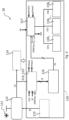
- Figure 1 discloses a regulated supply domain, RSD 110 of System On Chip, SOC architecture 10, that does not include a feature for achieving control of power absorption and performance, which may result in faster battery depletion and reduced performance.
- the SOC architecture 10 and of the regulated supply domain 110 are powered via a voltage supply 111 (i.e., a battery, for instance, a coin battery at a voltage VS), which is coupled to a power management unit (PMU) 112.
- a voltage supply 111 i.e., a battery, for instance, a coin battery at a voltage VS
- PMU power management unit
- the power management unit 112 is powered by the battery 111 and is configured to receive a supply feedback signal SF from a power grid 113 and to output a current control signal CS to a regulator 114.
- the regulator 114 is configured to regulate the voltage of the regulated supply domain 110, and the current control signal CS is also applied to a consumption detector 115.
- the consumption detector CD 115 is configured to monitor the amount of current in the RSD 110 and to provide a current evaluation signal CE to a power control logic unit 116.
- the power control logic unit 116 is configured to receive the current evaluation signal CE as an input and to output, based on the state of the signal CE, a power status signal PS (for instance, run, low power run, standby, etc.,) that is then provided to a clock controller, CC 117.
- a power status signal PS for instance, run, low power run, standby, etc.
- the clock controller, CC 117 is configured to generate, according to the input power status signal PS received from the power control logic unit 116, a plurality of different clock signals CK1, CK2, ..., CKk that are provided to a plurality of (peripheral) clock domains 118 1 , 118 2 , ..., 118 k .
- Figure 2 shows a possible implementation of a clock controller 117 as illustrated in Figure 1 having coupled therewith a plurality of peripherals 18 11 , 18 12 , ..., 18 1k to 18 N1 , 18 N2 , ..., 18 Nk .
- peripherals may be in any number and include, by way of example, master or slave peripherals that may be managed by standard/custom buses, for instance, AHB (Advanced High-performance Bus), APB ("Advanced Peripheral Bus"), or any others (OBI "Open Bus Interface”, AXI "Advanced eXtensible Interface”, etc.).
- AHB Advanced High-performance Bus
- APB Advanced Peripheral Bus
- OBI Open Bus Interface
- AXI Advanced eXtensible Interface
- the clock controller 117 is configured to receive from the power control logic unit 116 a power status signal PS (see the diagram of Figure 1 ) and to apply that signal PS to a clock controller logic and register block 151 included in the clock controller 117.
- the clock controller 117 illustrated in Figure 2 does not provide for absorption control, which may lead to fast battery depletion and reduced performance.
- the block 151 is configured to calculate and provide as its outputs:
- the oscillators 16 1 , ..., 16 N are configured to provide their respective generated clock signals to respective sets of gating blocks 17 11 , 17 12 , ..., 17 1k to 17 N1 , 17 N2 , ..., 17 Nk .
- the sets of gating blocks 17 11 , 17 12 , ..., 17 1k to 17 N1 , 17 N2 , ..., 17 Nk are configured to be clocked by the clock signals generated by the respective oscillators 16 1 , ..., 16 N and receive the gating values gc 11 , ..., gc Nk provided by the clock controller logic and registers block 151, to output respective sets of gated clock signals CK11, CK12, ..., CK1k to CKN1, CKN2, ..., CK1M to the peripherals 18 11 , 18 12 , ..., 18 1k to 18 N1 , 18 N2 , ..., 18 Nk respectively coupled therewith.
- various embodiments of the present disclosure provide solutions for a regulated supply domain of System On Chip architecture with a power saving feature: for a general description of a regulated supply domain in conventional System On Chip architecture, reference can be made to the previous description of Figures 1 and 2 .
- Figure 3 is a block diagram showing a regulated supply domain 20 in System On Chip architecture according embodiment of the present disclosure.
- the regulated supply domain 20 illustrated in Figure 3 includes, together with parts or elements that may be unchanged with respect to Figure 1 :
- the consumption detector CD 215, 215' receives as input values the current control signal CS, a clock signal CLK, and a count start flag SC: for instance, this may be via an Advanced High-performance, AHB bus and the representation of the AHB as a separate entity in Figure 3 is merely functional and for the sake of clarity.
- FIGS. 4A and 4B are block diagrams showing certain features of a consumption detector CD 215, 215' according to embodiments of the present disclosure.
- the consumption detector CD 215 of Figure 4A includes two threshold registers, 131 and 132, which are configured to have stored therein the values for two thresholds, a first threshold Imax1 reg and a second threshold Imax2 reg , respectively. These are an upper threshold and a lower threshold, respectively, that may be set according to battery specification or introduced by the user, for instance, to be sure that a specific task uses current values that do not reach threshold values determined by the user, for instance, in case of particular applications.
- the threshold registers 131, 132 may be accessible, for instance, for both read and write operations, through a standard bus interface 134, for instance, an AHB bus or a different standard bus, and may be configured to receive a POR ("Power-On Reset") signal to reset the value contained in the threshold registers 131, 132 when a reset event occurs.
- a standard bus interface 134 for instance, an AHB bus or a different standard bus
- the threshold registers 131, 132 are coupled with a current detector block 133 that is configured to receive as input values such first threshold Imax1 reg and second threshold Imax2 reg stored in the threshold registers 131, 132, the current control signal CS, and the POR signal.
- the current detector block 133 is configured to compare a currently available current I, obtained from the current control signal CS, with the first threshold Imax1 reg and the second threshold Imax2 reg received as input.
- the current detector block 133 may be configured to:
- the first flag Imax1 and second flag Imax2 indicate if the currently available current I, i.e., the current consumption, is over a threshold, for instance, over the first threshold Imax1 reg and (also) over the second threshold Imax2 reg , respectively.
- the current detector block 133 can be configured to provide as its outputs the value of the first flag Imax1 and the value of the second flag Imax2 continuously. These outputs are then forwarded as outputs of the consumption detector CD 215.
- FIG. 4B is a block diagram showing a consumption detector CD 215' according to another embodiment of the present disclosure.
- the consumption detector CD 215' of Figure 4B may optionally contain two counter registers, 137 and 140, that are configured to contain the values of two counters, a first counter CImax1 reg and a second counter CImax2 reg , respectively.
- the first counter CImax1 reg when enabled, is configured to count the number of clock periods in which the condition I ⁇ Imax 1 reg is satisfied, while the second counter CImax2 reg , when enabled, is configured to count the number of clock periods in which the condition I ⁇ Imax 2 reg is satisfied.
- the counter registers 137, 140 may be accessible, for instance, for both read and write operations, through a standard bus interface 134, for instance, the AHB bus or a different standard bus, and they may be configured to receive a reset signal rC from the bus interface 134 to reset the value contained in the counter registers 137, 140.
- the consumption detector, CD 215' is further configured to receive the clock signal CLK and the count start flag SC as input signals.
- the count start flag SC is coupled with AND logic gates 135, and 138 and it is used to enable the count of the conditions I ⁇ Imax 1 reg , and I ⁇ Imax 2 reg , respectively.
- the AND gate 135 is configured to receive at its inputs the first flag Imax1 and, as previously described, the count start flag SC which is used as a masking signal for the first flag Imax1.
- the output of the AND gate 135 is set in response to both the first flag Imax1 and the count start flag SC being set, and is provided as input to a clock gating block 136.
- the clock gating block 136 is configured to receive as input the output of the AND gate 135 and the clock signal CLK, and provides as output a gated clock that is used to drive the counter register 137.
- the output of the AND gate 138 is set in response to both the second flag Imax2 and the count start flag SC being set, and is provided as input to a clock gating block 139.
- the clock gating block 139 is configured to receive as input the output of the AND gate 138 and the clock signal CLK, and provides as output a gated clock that is used to drive the counter register 140.
- circuitry that differentiates the embodiment of Figure 4B from the embodiment of Figure 4A provide for the possibility of having an insight of the effective number of times in which the first and second flags Imax1 and Imax2 are set.
- FIG. 5 is a block diagram showing a clock controller 25 and peripherals 18 11 , 18 12 , ..., 18 1k to 18 N1 , 18 N2 , ..., 18 Nk , coupled therewith.
- these may be, for instance, master or slave peripherals such as AHB ("Advanced High-performance Bus") or APB ("Advanced Peripheral Bus”) peripherals.
- AHB Advanced High-performance Bus
- APB Advanced Peripheral Bus
- the solutions described herein include a clock controller, CC 217 with a set of clock division factors calculated by a clock controller SCC to be then applied to modify peripheral consumption, reducing the operating frequencies of the peripherals by modifying the clocks applied thereto, which leads to a more accurate control of power consumption and performance.
- the oscillators 16 1 , ..., 16 N are configured to generate respective clock signals according to a respective received oscillator frequency and a respective run value.
- the oscillators 16 1 , ..., 16 N are configured to provide the respective generated clock signal to an intermediate clock divider block 19 1 , ..., 19 N .
- the intermediate clock divider block 19 1 , ..., 19 N is configured to receive as inputs the respective clock signals and clock divide factors N 1 , ..., N k , and is configured to provide as an output a divided clock signal which is then provided to respective sets of gating blocks 17 11 , 17 12 , ..., 17 1k to 17 N1 , 17 N2 , ..., 17 Nk .
- the clock divide factors N 1 , ..., N k are computed in a circuit 266 taking into account clock constraints and then stored in dedicated registers associated therewith.
- the circuit 266 is configured to act as a "smart" clock controller SCC and will be referred to in the following either as SCC or, briefly, as clock controller.
- the method cannot change the original clock phases and the clock gating policy.
- the clock controller circuit 266 (SCC) is configured to receive as inputs the first flag Imax1, the second flag Imax2, the power status signal PS, and the mode signal M, and is configured to provide as its output an interrupt INT which may be maskable to core and the set of such clock divide factors N 1 , ..., N k .
- the clock controller 266 may implement a method to determine certain sets of clock division factors, for instance, with the possibility to applying fixed clock dividers for certain functions held to be critical.
- FIG. 6 is a block diagram of a "smart" clock controller 266 according to embodiments of the present disclosure.
- the clock controller 266 is configured to be coupled to the bus interface 134, for instance, an Advanced High-performance Bus (AHB), Open Bus Interface (OBI), Advanced eXtensible Interface (AXI), or other types of standard interfaces, and to receive at its inputs:
- ABB Advanced High-performance Bus
- OBI Open Bus Interface
- AXI Advanced eXtensible Interface
- the clock controller 266 is configured to provide as an output:
- the input signals received by the clock controller SCC 266 are forwarded as inputs to a control register 271.
- the control register 271 is coupled to the bus interface 134 which is used, for instance, by a core, to configure such control register 271, for instance, to read/write sets of registers.
- the control register 271 is further coupled to sets of registers RS 272 1 , ..., 272 2 , 272 i , ..., 272 j , ..., 272 M each of them containing the values of the clock divide factors N 1 , ..., N k to be used for each different power scenario plus some others used for special purposes.
- Exemplary possible sets of registers may include:
- the registers in the sets of registers exemplified above, collectively referred to as 272 in the following, are coupled to inputs of a multiplexer 277.
- control register 271 is configured to manage the selection of registers in the sets collectively referred to as 272 based on the received input mode signal M.
- control register 271 generates a selection signal SEL which is forwarded to the multiplexer 277 to select the multiplexer inputs, namely, the set of registers, for instance, 272 1 , to be used and that can be coupled with the output of the multiplexer.
- SEL selection signal
- the output from the multiplexer 277 is provided as an output from the ("smart") clock controller 266 which identifies the set of clock divide factors N 1 , ..., N k related to the currently used power mode M.
- control register 271 can also generate an interrupt INT, which is then forwarded to the clock controller SCC 266.
- the input mode signal M may have, by way of example, one of the following contents/meanings:
- the mode signal M to the clock controller 266 can be set to a forced mode and used to optimize the configuration in use and to optimize power and performance in "special operation" conditions.
- a forced mode is selected (via a system core, for instance) before or during the "special operation" conditions or, alternatively, designer/architect can select the forced mode with special hardware configurations, for instance, when the core is off for low power mode.
- Non-limiting examples of “special operation” may be:
- a forced mode can be selected even when an interrupt INT is raised due to overconsumption, for instance, or due to a rare/unexpected event occurring such as low power or performance emergency, i.e., battery level is very low.
- the system core can also be configured to store the calculated values of the clock divide factors N 1 , ..., N k in a non-volatile memory associated with the core, for instance, a Flash, PCM ("Phase-change memory”), or OTP ("One Time Programmable”), etc. memory.
- a non-volatile memory for instance, a Flash, PCM ("Phase-change memory”), or OTP ("One Time Programmable”), etc. memory.
- the core may load the sets of registers RS 272 with non-volatile values for the clock divide factors N 1 , ..., N k previously stored in the non-volatile memory by the core.
- POR power on reset
- a possible tuning criterion is a trial-and-error approach that can be implemented on a "one time” basis, once system architecture is devised.
- the calculated clock divide factors N 1 , ..., N k may be also applied to the whole, or a part of, production of the same system architecture.
- the calculated clock divide factors N 1 , ..., N k may be also applied as default value to the products with the same system architecture to be further refined by the users according to their particular needs and applications implemented.
- Exemplary steps that can may be considered for implementing such a tuning criterion are the following:
- the trial-and-error approach procedure continues until the target consumption and performance are reached via additional steps including:
- An example of a second tuning criterion is an automatic approach.
- tuning of the clock divide factors N 1 , ..., N k values may be done directly by the SOC core via different approaches, for instance, simulated annealing, tabu search, etc.
- optimal clock divide factors N 1opt , ..., N kopt can be found by solving an optimization problem and saving the resulting optimal clock divide factors N 1opt , ..., N kopt in a set of registers out of the sets of registers corresponding to the power mode used, that is to the power status signal PS.
- the cost function may contain also other measurements that are available on the SOC.
- minimization of such a cost function may be performed using different minimization techniques, for instance, simulated annealing, tabu search, etc. Such techniques to find the minimum of a function are well-known in the art, and will not be described in detail herein to not overburden the present detailed description.
- the process is repeated again from the first step, for instance after changing randomly a few of the clock divide factors N 1 , ..., N k in the specific set of registers of the sets of registers 272, and the loop is repeated (even a large number of times such as a thousand times).
- the values stored in the specific set of registers of the sets of registers 272 which is expected to contain optimal clock divide factors N 1opt , ..., N kopt are optimal clock divide factors sought N 1opt , ..., N kopt .
- These optimal clock divide factors N 1opt , ..., N kopt are stored in a set of registers out of the sets of registers 272 at the end of the computation procedure. The values are "frozen" and used in the specific real scenario for what they were calculated.
- different sets of optimal clock divide factors N 1opt , ..., N kopt can be computed for different scenarios, for instance, by using different metrics or for different performance/battery life balances. Prior to starting a particular task related to one of such different scenarios, the corresponding optimal clock divide factors N 1opt , ..., N kopt for that scenario are used to replace the default ones.
- Various embodiments may adopt different arrangements for storing the optimal clock divide factors N 1opt , ..., N kopt .
- the optimal clock divide factors N 1opt , ..., N kopt computed may be stored in a non-volatile memory, for instance, Flash, PCM, OTP, etc., and retrieved after each power cycle to be stored in a corresponding specific set of registers of the sets of registers 272.
- the optimal clock divide factors N 1opt , ..., N kopt computed may be retained in non-volatile registers. Such a solution may be used for instance, in flash-less products.
- the optimal clock divide factors N 1opt , ..., N kopt once first computed, can be re-calculated at each power cycle. Such a solution may be considered for instance, for devices that remain always on and that are switched off a few times a year.
- the solution provided herein discloses a consumption detector, CD and a clock controller, CC with a set of clock division factors applied to modify consumption.
- the consumption detector, CD uses two threshold registers to store two current thresholds, Imax1 reg and Imax2 reg , which are used as a comparison for an absorbed current. In response to these thresholds Imax1 reg and Imax2 reg , being exceeded a certain set of dividers of the clocks is selected and applied.
- Division factors are calculated by a "smart" clock controller, SCC, that is circuit included in the clock controller, CC, circuitry in order to reduce the consumption by reducing a peripherals operating frequency.
- the "smart" clock controller, SCC may additionally comprise a learning procedure to determine the sets of (sub)optimal clock division factors for considered scenarios.
- the solution as described herein facilitates achieving a balance between current consumption and performance, and in some embodiments, the balance between consumption and performance may be obtained to different degrees using different cost functions in learning procedures.
Landscapes
- Engineering & Computer Science (AREA)
- Theoretical Computer Science (AREA)
- Physics & Mathematics (AREA)
- General Engineering & Computer Science (AREA)
- General Physics & Mathematics (AREA)
- Power Sources (AREA)
Abstract
Description
- The description relates to electronic circuits.
- One or more embodiments can be applied to electronic circuits such as, for instance, System On Chip, SOC circuits with power-saving features.
- Certain electronic devices such as portable devices like cellular phones are unable to support prolonged high power consumption conditions due to battery limitations.
- A control of power absorption and performance may effectively counter waste of energy and at the same time improve performance under energy constraints.
- A dynamic balance of power absorption and performance, possibly detecting unnecessary/undesired extra power consumption and facilitating low power consumption (whenever this does not result in undesired performance degradation) may thus represent a goal to pursue in these applications.
- Solutions with balanced current consumption and performance, especially with applications unable to support high current consumption for a long time, due to battery limitations, for instance, are thus desirable.
- An object of one or more embodiments is to contribute in providing such a solution.
- According to one or more embodiments, that object is achieved via a circuit (a system on chip, SOC circuit, for instance) having the features set forth in the claims that follow.
- One or more embodiments concern a related configuration method.
- The claims are an integral part of the technical teaching provided in respect of the embodiments.
- Solutions as described herein include a consumption detector, CD and a clock controller, CC with a set of clock division factors applied to control consumption.
- For instance, in exemplary solutions as described herein, a consumption detector, CD uses two threshold registers to save two current values Imax1reg and Imax2reg; these represent an upper threshold and a lower threshold, respectively, that can be set according to battery specifications. A current absorbed is compared with these two thresholds and, based on the result of comparison with these thresholds Imax1reg and Imax2reg, a set of parameters (dividers of the clocks) is selected and applied.
- In exemplary solutions as described herein:
- division factors can be calculated by a clock controller, SCC, contained within the clock controller, CC, in order to reduce consumption by reducing an operating frequency by modifying the clocks, and
- the clock controller, SCC may implement a learning procedure to determine certain sets of clock division factors, for instance, with the possibility of applying fixed clock dividers for certain functions held to be critical.
- Solutions as described herein facilitate achieving a judicious trade-off between current consumption and performance.
- One or more embodiments will now be described, by way of example only, with reference to the annexed figures, wherein:
-
Figure 1 is a block diagram of a regulated supply domain in System On Chip, SOC architecture; -
Figure 2 is a block diagram of a clock controller and peripherals coupled therewith; -
Figure 3 is a block diagram of a regulated supply domain in System On Chip architecture according to embodiments of the present disclosure; -
Figure 4A andFigure 4B are block diagrams of a consumption detector according to embodiments of the present disclosure; -
Figure 5 is a block diagram of a clock controller and associated peripherals according to embodiments of the present disclosure; and -
Figure 6 is a block diagram of a clock controller according to embodiments of the present disclosure. - Corresponding numerals and symbols in the different figures generally refer to corresponding parts unless otherwise indicated.
- The figures are drawn to clearly illustrate the relevant aspects of the embodiments and are not necessarily drawn to scale.
- The edges of features drawn in the figures do not necessarily indicate the termination of the extent of the feature.
- In the ensuing description one or more specific details are illustrated, aimed at providing an in-depth understanding of examples of embodiments of this description. The embodiments may be obtained without one or more of the specific details, or with other methods, components, materials, etc. In other cases, known structures, materials, or operations are not illustrated or described in detail so that certain aspects of embodiments will not be obscured.
- Reference to "an embodiment" or "one embodiment" in the framework of the present description is intended to indicate that a particular configuration, structure, or characteristic described in relation to the embodiment is comprised in at least one embodiment. Hence, phrases such as "in an embodiment" or "in one embodiment" that may be present in one or more points of the present description do not necessarily refer to one and the same embodiment.
- Moreover, particular configurations, structures, or characteristics may be combined in any adequate way in one or more embodiments.
- The headings/references used herein are provided merely for convenience and hence do not define the extent of protection or the scope of the embodiments.
- For simplicity and ease of explanation, throughout this description, and unless the context indicates otherwise, like parts or elements are indicated in the various figures with like reference signs, and a corresponding description will not be repeated for each and every figure.
-
Figure 1 discloses a regulated supply domain, RSD 110 of System On Chip,SOC architecture 10, that does not include a feature for achieving control of power absorption and performance, which may result in faster battery depletion and reduced performance. - The
SOC architecture 10 and of the regulatedsupply domain 110 are powered via a voltage supply 111 (i.e., a battery, for instance, a coin battery at a voltage VS), which is coupled to a power management unit (PMU) 112. - The
power management unit 112 is powered by thebattery 111 and is configured to receive a supply feedback signal SF from apower grid 113 and to output a current control signal CS to aregulator 114. - The
regulator 114 is configured to regulate the voltage of the regulatedsupply domain 110, and the current control signal CS is also applied to aconsumption detector 115. - The
consumption detector CD 115 is configured to monitor the amount of current in theRSD 110 and to provide a current evaluation signal CE to a powercontrol logic unit 116. - The power
control logic unit 116 is configured to receive the current evaluation signal CE as an input and to output, based on the state of the signal CE, a power status signal PS (for instance, run, low power run, standby, etc.,) that is then provided to a clock controller,CC 117. - The clock controller, CC 117 is configured to generate, according to the input power status signal PS received from the power
control logic unit 116, a plurality of different clock signals CK1, CK2, ..., CKk that are provided to a plurality of (peripheral)clock domains -
Figure 2 shows a possible implementation of aclock controller 117 as illustrated inFigure 1 having coupled therewith a plurality ofperipherals - These peripherals may be in any number and include, by way of example, master or slave peripherals that may be managed by standard/custom buses, for instance, AHB (Advanced High-performance Bus), APB ("Advanced Peripheral Bus"), or any others (OBI "Open Bus Interface", AXI "Advanced eXtensible Interface", etc.).
- The
clock controller 117 is configured to receive from the power control logic unit 116 a power status signal PS (see the diagram ofFigure 1 ) and to apply that signal PS to a clock controller logic andregister block 151 included in theclock controller 117. - The
clock controller 117 illustrated inFigure 2 does not provide for absorption control, which may lead to fast battery depletion and reduced performance. - As illustrated In
Figure 2 , theblock 151 is configured to calculate and provide as its outputs: - oscillator frequencies f_regclk1, ..., f_regclkN (collectively designated OF);
- oscillator run values runclk1, ..., runclkN (collectively designated OR), and
- gating values gc11, ..., gcNk (collectively designated G) .
- The oscillator frequencies OF and the oscillator run values OR are provided as input to respective oscillators labelled 161, ..., 16N. Each oscillator 161, ..., 16N generates a different clock signal for
different clock domains - The oscillators 161, ..., 16N are configured to provide their respective generated clock signals to respective sets of
gating blocks - The sets of
gating blocks registers block 151, to output respective sets of gated clock signals CK11, CK12, ..., CK1k to CKN1, CKN2, ..., CK1M to theperipherals - As discussed, various embodiments of the present disclosure provide solutions for a regulated supply domain of System On Chip architecture with a power saving feature: for a general description of a regulated supply domain in conventional System On Chip architecture, reference can be made to the previous description of
Figures 1 and2 . -
Figure 3 is a block diagram showing a regulatedsupply domain 20 in System On Chip architecture according embodiment of the present disclosure. - For brevity and ease of understanding, in
Figures 3 to 6 parts or elements like parts or elements already described in connection withFigures 1 and2 are denoted by the same reference symbols already appearing inFigure 1 and2 and a detailed description of these parts or elements will not be repeated in the following. - By way of direct comparison with
Figure 1 , the regulatedsupply domain 20 illustrated inFigure 3 includes, together with parts or elements that may be unchanged with respect toFigure 1 : - a consumption detector, CD - this may be, for instance, either the
consumption detector 215 ofFigure 4A or the consumption detector 215' ofFigure 4B - that is configured to replace theconsumption detector 115 ofFigure 1 , and - a clock controller,
CC 217 that is configured to replace theclock controller 117 ofFigure 1 . - As illustrated in
Figures 3 ,4A , and4B theconsumption detector CD 215, 215' receives as input values the current control signal CS, a clock signal CLK, and a count start flag SC: for instance, this may be via an Advanced High-performance, AHB bus and the representation of the AHB as a separate entity inFigure 3 is merely functional and for the sake of clarity. - As illustrated in
Figures 3 ,4A , and4B : - the
consumption detector CD 215, 215' is configured to provide as outputs the current evaluation signal CE, a first flag Imax1, and a second flag Imax2; and - the
clock controller CC 217 is configured to be coupled to the AHB bus and to receive as input values the first flag Imax1, the second flag Imax2, a power status signal PS, and a mode signal M. In addition, it is configured to provide as outputs such plurality of different clock signals CK1, CK2, ..., CKk and, optionally, an interrupt INT which may be maskable to core. -
Figures 4A and4B are block diagrams showing certain features of aconsumption detector CD 215, 215' according to embodiments of the present disclosure. - For simplicity, features left unchanged with respect to
Figure 1 are not visible inFigures 4A and4B . - The
consumption detector CD 215 ofFigure 4A includes two threshold registers, 131 and 132, which are configured to have stored therein the values for two thresholds, a first threshold Imax1reg and a second threshold Imax2reg, respectively. These are an upper threshold and a lower threshold, respectively, that may be set according to battery specification or introduced by the user, for instance, to be sure that a specific task uses current values that do not reach threshold values determined by the user, for instance, in case of particular applications. - The threshold registers 131, 132 may be accessible, for instance, for both read and write operations, through a
standard bus interface 134, for instance, an AHB bus or a different standard bus, and may be configured to receive a POR ("Power-On Reset") signal to reset the value contained in the threshold registers 131, 132 when a reset event occurs. - The threshold registers 131, 132 are coupled with a
current detector block 133 that is configured to receive as input values such first threshold Imax1reg and second threshold Imax2reg stored in the threshold registers 131, 132, the current control signal CS, and the POR signal. - As illustrated, the
current detector block 133 is configured to compare a currently available current I, obtained from the current control signal CS, with the first threshold Imax1reg and the second threshold Imax2reg received as input. - For instance, the
current detector block 133 may be configured to: - compare the value of the currently available current I with the first threshold Imax1reg and if the condition I ≥ Imax1 reg is satisfied, the value of a first flag Imax1 is set to 1, otherwise it is set to 0; and
- compare the value of the currently available current I with the second threshold Imax2reg and if the condition I ≥ Imax2 reg is satisfied, the value of a second flag Imax2 is set to 1, otherwise it is set to 0.
- Thus, the first flag Imax1 and second flag Imax2 indicate if the currently available current I, i.e., the current consumption, is over a threshold, for instance, over the first threshold Imax1reg and (also) over the second threshold Imax2reg, respectively.
- Hence, the
current detector block 133 can be configured to provide as its outputs the value of the first flag Imax1 and the value of the second flag Imax2 continuously. These outputs are then forwarded as outputs of theconsumption detector CD 215. -
Figure 4B is a block diagram showing a consumption detector CD 215' according to another embodiment of the present disclosure. In addition to the components already described inFigure 4A (these will not be described again in the following in order not to overburden the present detailed description) the consumption detector CD 215' ofFigure 4B may optionally contain two counter registers, 137 and 140, that are configured to contain the values of two counters, a first counter CImax1reg and a second counter CImax2reg, respectively. - The first counter CImax1reg, when enabled, is configured to count the number of clock periods in which the condition I ≥ Imax1 reg is satisfied, while the second counter CImax2reg, when enabled, is configured to count the number of clock periods in which the condition I ≥ Imax2 reg is satisfied.
- The counter registers 137, 140 may be accessible, for instance, for both read and write operations, through a
standard bus interface 134, for instance, the AHB bus or a different standard bus, and they may be configured to receive a reset signal rC from thebus interface 134 to reset the value contained in the counter registers 137, 140. The consumption detector, CD 215' is further configured to receive the clock signal CLK and the count start flag SC as input signals. - The count start flag SC is coupled with AND
logic gates - The AND
gate 135 is configured to receive at its inputs the first flag Imax1 and, as previously described, the count start flag SC which is used as a masking signal for the first flag Imax1. - The output of the AND
gate 135 is set in response to both the first flag Imax1 and the count start flag SC being set, and is provided as input to aclock gating block 136. - As illustrated, the clock gating block 136 is configured to receive as input the output of the AND
gate 135 and the clock signal CLK, and provides as output a gated clock that is used to drive thecounter register 137. - Similarly, the output of the AND
gate 138 is set in response to both the second flag Imax2 and the count start flag SC being set, and is provided as input to aclock gating block 139. - The clock gating block 139 is configured to receive as input the output of the AND
gate 138 and the clock signal CLK, and provides as output a gated clock that is used to drive thecounter register 140. - The circuitry that differentiates the embodiment of
Figure 4B from the embodiment ofFigure 4A provide for the possibility of having an insight of the effective number of times in which the first and second flags Imax1 and Imax2 are set. -
Figure 5 is a block diagram showing a clock controller 25 andperipherals - In the following, elements or components which have already been described with reference to the previous figures are denoted by the same references previously used in these figures. A description of these elements already described previously will not be repeated in order not to overburden the present detailed description.
- The solutions described herein include a clock controller,
CC 217 with a set of clock division factors calculated by a clock controller SCC to be then applied to modify peripheral consumption, reducing the operating frequencies of the peripherals by modifying the clocks applied thereto, which leads to a more accurate control of power consumption and performance. - In the embodiment illustrated in
Figure 5 , the oscillators 161, ..., 16N are configured to generate respective clock signals according to a respective received oscillator frequency and a respective run value. - In the embodiment illustrated in
Figure 5 , the oscillators 161, ..., 16N are configured to provide the respective generated clock signal to an intermediate clock divider block 191, ..., 19N. - The intermediate clock divider block 191, ..., 19N is configured to receive as inputs the respective clock signals and clock divide factors N1, ..., Nk, and is configured to provide as an output a divided clock signal which is then provided to respective sets of gating blocks 1711, 1712, ..., 171k to 17N1, 17N2, ..., 17Nk.
- As illustrated herein, the clock divide factors N1, ..., Nk, are computed in a
circuit 266 taking into account clock constraints and then stored in dedicated registers associated therewith. - The
circuit 266 is configured to act as a "smart" clock controller SCC and will be referred to in the following either as SCC or, briefly, as clock controller. - A non-limiting example of a clock constraints that can be taken into account in computing clock division factors N1, ..., Nk is, for instance, α1fclk1 > α2fclk2, etc. wherein some of the αx factors may be rational αx = px/qx.
- Moreover, a configuration of the clock division factors N1, ..., Nk such as N1 = 0, ..., Nk = 0 may be regarded as inadmissible.
- In a default configuration of the clock division factors N1, ..., Nk, the value associated with such clock division factors N1, ..., Nk is N1 = 1, ..., Nk = 1 which is called the "legacy condition". In the legacy condition, the method cannot change the original clock phases and the clock gating policy.
- As illustrated in
Figure 6 , the clock controller circuit 266 (SCC) is configured to receive as inputs the first flag Imax1, the second flag Imax2, the power status signal PS, and the mode signal M, and is configured to provide as its output an interrupt INT which may be maskable to core and the set of such clock divide factors N1, ..., Nk. - In addition, the
clock controller 266 may implement a method to determine certain sets of clock division factors, for instance, with the possibility to applying fixed clock dividers for certain functions held to be critical. -
Figure 6 is a block diagram of a "smart"clock controller 266 according to embodiments of the present disclosure. - As previously stated, the
clock controller 266 is configured to be coupled to thebus interface 134, for instance, an Advanced High-performance Bus (AHB), Open Bus Interface (OBI), Advanced eXtensible Interface (AXI), or other types of standard interfaces, and to receive at its inputs: - the first flag Imax1 and the second flag Imax2, which are provided by the
consumption detector CD 215, and that indicate over threshold events, - the power status signal PS, for instance, run, low power run, standby, etc., received from the power
control logic unit 116; and - the mode M, for instance, transparent, set/reset, active, forced, etc.
- As illustrated, the
clock controller 266 is configured to provide as an output: - the interrupt INT, whenever the first flag Imax1 and/or the second flag Imax2 are set, which is sent to a core and that may be maskable to such core; and
- the set of clock divide factors N1, ..., Nk that are currently in use, i.e., corresponding to the current mode M in use.
- The input signals received by the
clock controller SCC 266 are forwarded as inputs to acontrol register 271. Thecontrol register 271 is coupled to thebus interface 134 which is used, for instance, by a core, to configuresuch control register 271, for instance, to read/write sets of registers. - The
control register 271 is further coupled to sets ofregisters RS 2721, ..., 2722, 272i, ..., 272j, ..., 272M each of them containing the values of the clock divide factors N1, ..., Nk to be used for each different power scenario plus some others used for special purposes. - Exemplary possible sets of registers may include:
- a
set RS 1 2721, which contains (in k positions) clock divide factors (N1, ..., Nk)1 for use in a run mode; - a
set RS 2 2722, which contains (in k positions) clock divide factors (N1, ..., Nk)2 for use in a low-power run mode; -
sets RS i 272i to 272j, which contain (in k positions) clock divide factors (N1, ..., Nk)i to (N1, ..., Nk)j for use in running various subtasks; and - a
set RS M 272M, for instance, learning registers, which contain (in k positions) clock divide factors (N1, ..., Nk)M for use in a learning mode. - The registers in the sets of registers exemplified above, collectively referred to as 272 in the following, are coupled to inputs of a
multiplexer 277. - As illustrated, the
control register 271 is configured to manage the selection of registers in the sets collectively referred to as 272 based on the received input mode signal M. - As illustrated, the
control register 271 generates a selection signal SEL which is forwarded to themultiplexer 277 to select the multiplexer inputs, namely, the set of registers, for instance, 2721, to be used and that can be coupled with the output of the multiplexer. - The output from the
multiplexer 277 is provided as an output from the ("smart")clock controller 266 which identifies the set of clock divide factors N1, ..., Nk related to the currently used power mode M. - In addition, the
control register 271 can also generate an interrupt INT, which is then forwarded to theclock controller SCC 266. - The input mode signal M may have, by way of example, one of the following contents/meanings:
- transparent, namely a default state where the clock division factors N1, ..., Nk are equal to those of the "legacy condition", for instance N1 = 1, ..., Nk = 1;
- set/reset, namely a condition where the content of the sets of registers can be modified, for instance, from the AHB bus, with learning registers copied in one set of registers in the sets of registers;
- active, namely a condition where the set of registers to be used is selected automatically according to the current power status signal PS from the power
control logic unit 116; - forced, namely a condition where the set of registers to be used is imposed by the core, by using the bus interface, for instance, when it is desired to select a set of registers that contains clock divide factors to be used during the run of a specific subtask; and
- learning, which can be programmed in a plurality of different ways, according to the method used for the computation of the clock divide factors.
- The mode signal M to the
clock controller 266 can be set to a forced mode and used to optimize the configuration in use and to optimize power and performance in "special operation" conditions. - In that case, a forced mode is selected (via a system core, for instance) before or during the "special operation" conditions or, alternatively, designer/architect can select the forced mode with special hardware configurations, for instance, when the core is off for low power mode.
- Non-limiting examples of "special operation" may be:
- a run operation while receiving/transmitting data from/to a radio interface, for instance, a UWB (Ultra-Wide Band) modem, when it is desired that operation consumption should be maintained below a given threshold;
- a run operation while a crypt/decrypt operation is in progress, for instance, with both the crypto hardware and the core running;
- a low-power run operation while the radio interface, for instance, a UWB modem, is off and a wired interface(s) is/are receiving some data.
- In addition, a forced mode can be selected even when an interrupt INT is raised due to overconsumption, for instance, or due to a rare/unexpected event occurring such as low power or performance emergency, i.e., battery level is very low.
- The system core refer to herein can also be configured to store the calculated values of the clock divide factors N1, ..., Nk in a non-volatile memory associated with the core, for instance, a Flash, PCM ("Phase-change memory"), or OTP ("One Time Programmable"), etc. memory.
- Then, at each power cycle reset event POR, the calculated values of the clock divide factors N1, ..., Nk stored within the sets of
registers RS 272 are preset to the "legacy condition", i.e., N1, ..., Nk is N1 = 1, ..., Nk = 1. - Once a power on reset (POR) sequence is completed, the core may load the sets of
registers RS 272 with non-volatile values for the clock divide factors N1, ..., Nk previously stored in the non-volatile memory by the core. - Different tuning criteria can be used in order to tune in an efficient way the clock divide factors N1, ..., Nk.
- In the following, certain non-limiting examples of tuning criteria that can be used will be described by way of example.
- A possible tuning criterion is a trial-and-error approach that can be implemented on a "one time" basis, once system architecture is devised.
- Therefore, once the clock divide factors N1, ..., Nk are calculated in a first testing phase of the system architecture, the calculated clock divide factors N1, ..., Nk may be also applied to the whole, or a part of, production of the same system architecture. In addition, the calculated clock divide factors N1, ..., Nk may be also applied as default value to the products with the same system architecture to be further refined by the users according to their particular needs and applications implemented.
- In such a case, multiple "experiments" are performed increasing one-by-one the values of the clock divide factors N1, ..., Nk, and storing, for each of the attempts, a value for the first counter CImax1reg, a value for the second counter CImax2reg, and the execution time.
- In that way, after a set of experiments, it is possible to select combinations of clock divide factors N1, ..., Nk values that lead to reduced count values for the first and the second counter CImax1reg and CImax2reg, while leaving the execution time involved substantially unchanged.
- Exemplary steps that can may be considered for implementing such a tuning criterion are the following:
- first step: the input mode signal M is set to a "learning" mode and the learning registers in the
set 272M are set to the "legacy condition", i.e., N1, ..., Nk is N1 = 1, ..., Nk = 1; - second step: the values of the two
counter registers - third step: the
SOC device 20 is configured to operate in a desired scenario and "optimized" by selecting a specific power mode, that is setting the power status signal PS, for instance, to run, low power run, standby, ecc. thus, preparing theSOC device 20 to execute one or more desired tasks; - fourth step: these tasks are executed on the SOC device; and
- fifth step: the values stored in the two counter registers CImax1reg and CImax2reg and the execution time at the end of execution of the one or more tasks are analyzed.
- If consumption and performance meet desired specifications, the calculated clock divide factors N1, ..., Nk stored within the learning registers set
RS M 272M are copied to the set of registers of the sets of registers corresponding to the power status signal PS that is currently used, i.e., the used power mode, and the procedure for the computation of the clock divide factors N1, ..., Nk values stops. - Alternatively, the trial-and-error approach procedure continues until the target consumption and performance are reached via additional steps including:
- sixth step: changing the value of the clock divide factors N1, ..., Nk in the learning registers set 272M, (taking into account possible clock constraints), for instance, incrementing one of the clock divide factors N1, ..., Nk by 1; and
- seventh step: running again the procedure starting from the second step.
- This approach results in a simple, yet long (quasi-manual) approach which can be useful for certain purposes.
- An example of a second tuning criterion is an automatic approach.
- In that case, tuning of the clock divide factors N1, ..., Nk values may be done directly by the SOC core via different approaches, for instance, simulated annealing, tabu search, etc.
- A problem to be solved can be defined as finding optimal clock divide factors N1opt, ..., Nkopt:

- Hence, optimal clock divide factors N1opt, ..., Nkopt can be found by solving an optimization problem and saving the resulting optimal clock divide factors N1opt, ..., Nkopt in a set of registers out of the sets of registers corresponding to the power mode used, that is to the power status signal PS.
- Such a problem can be solved via the following steps:
- determining a cost function describing the cost of execution of a/some particular task(s) as cost_function = f(CImax1, CImax2, Timeexecution ); and
- minimizing the cost function, bearing in mind that the first counter CImax1reg, the second counter CImax2reg, and the time of execution Timeexecution depend, in a nonlinear way, on the optimal clock divide factors N1opt, ..., Nkopt, and that inadmissible values for the (optimal) clock divide factors N1opt, ..., Nkopt due to clock constraints are discarded.
- In various embodiments, the cost function may contain also other measurements that are available on the SOC.
- The minimization of such a cost function may be performed using different minimization techniques, for instance, simulated annealing, tabu search, etc. Such techniques to find the minimum of a function are well-known in the art, and will not be described in detail herein to not overburden the present detailed description.
- By way of example, the following steps may be applied in a minimization technique of the simulated annealing for computing optimal clock divide factors N1opt, ..., Nkopt in the solution disclosed herein:
- first step: set in a random manner the values of the clock divide factors N1, ..., Nk in a specific set of registers of the sets of
registers 272 which is a candidate to containing optimal clock divide factors N1opt, ..., Nkopt. Some of the randomly drawn values of the clock divide factors N1, ..., Nk may be rational numbers, but in any case, inadmissible values due to clock constraints are discarded; - second step: execute one or more tasks on the SOC device; and
- third step: if the value of the cost function f(CImax1,CImax2,Timeexecution ) is lower than the cost function in the previous iteration, the current values of the clock divide factors N1, ..., Nk are accepted as new values, otherwise they are accepted with a probability p, to avoid remaining in a local minimum of the cost function.
- At the end of the third step, the process is repeated again from the first step, for instance after changing randomly a few of the clock divide factors N1, ..., Nk in the specific set of registers of the sets of
registers 272, and the loop is repeated (even a large number of times such as a thousand times). - At the end of looping, the values stored in the specific set of registers of the sets of
registers 272 which is expected to contain optimal clock divide factors N1opt, ..., Nkopt are optimal clock divide factors sought N1opt, ..., Nkopt. These optimal clock divide factors N1opt, ..., Nkopt are stored in a set of registers out of the sets ofregisters 272 at the end of the computation procedure. The values are "frozen" and used in the specific real scenario for what they were calculated. - Therefore, different sets of optimal clock divide factors N1opt, ..., Nkopt can be computed for different scenarios, for instance, by using different metrics or for different performance/battery life balances. Prior to starting a particular task related to one of such different scenarios, the corresponding optimal clock divide factors N1opt, ..., Nkopt for that scenario are used to replace the default ones.
- Various embodiments may adopt different arrangements for storing the optimal clock divide factors N1opt, ..., Nkopt.
- For instance, in various embodiments, the optimal clock divide factors N1opt, ..., Nkopt computed may be stored in a non-volatile memory, for instance, Flash, PCM, OTP, etc., and retrieved after each power cycle to be stored in a corresponding specific set of registers of the sets of
registers 272. - In other embodiments, the optimal clock divide factors N1opt, ..., Nkopt computed may be retained in non-volatile registers. Such a solution may be used for instance, in flash-less products.
- In still other embodiments, the optimal clock divide factors N1opt, ..., Nkopt, once first computed, can be re-calculated at each power cycle. Such a solution may be considered for instance, for devices that remain always on and that are switched off a few times a year.
- Thus, the solution provided herein discloses a consumption detector, CD and a clock controller, CC with a set of clock division factors applied to modify consumption.
- The consumption detector, CD uses two threshold registers to store two current thresholds, Imax1reg and Imax2reg, which are used as a comparison for an absorbed current. In response to these thresholds Imax1reg and Imax2reg, being exceeded a certain set of dividers of the clocks is selected and applied.
- Division factors are calculated by a "smart" clock controller, SCC, that is circuit included in the clock controller, CC, circuitry in order to reduce the consumption by reducing a peripherals operating frequency. The "smart" clock controller, SCC may additionally comprise a learning procedure to determine the sets of (sub)optimal clock division factors for considered scenarios.
- The solution as described herein facilitates achieving a balance between current consumption and performance, and in some embodiments, the balance between consumption and performance may be obtained to different degrees using different cost functions in learning procedures.
- Thus, the solution as described herein enables the realization of long-life battery devices without downgrading their performance.
- Without prejudice to the underlying principles, the details and the embodiments may vary, even significantly, with respect to what has been described by way of example only without departing from the scope of the embodiments.
- The extent of protection is determined by the annexed claims.
Claims (10)
- A circuit (20) comprising a plurality of peripherals (1811, 1812, ..., 181k; ...; 18N1, 18N2, ..., 18Nk) configured to be clocked with respective clock signals (CK11, CK12, ..., CKlk; ..., CKN1, CKN2, ..., CKNk), wherein the circuit (20) comprises a clock controller (217) configured (161, ..., 16N; 191, ..., 19N) to produce said respective clock signals (CK11, CK12, ..., CKlk; ..., CKN1, CKN2, ..., CKNk) via respective clock divide factors (N1, ..., Nk), the clock controller (217) having stored therein respective sets of clock divide factors (N1, ..., Nk), wherein the clock controller (217) comprises clock divide factor selection circuitry (266) configured to select (271, 277) an operating set of clock divide factors (N1, ..., Nk) out of said respective sets of clock divide factors (N1, ..., Nk) and wherein the clock controller (217) is configured (161, ..., 16N; 191, ..., 19N) to apply (277) to the plurality of peripherals (1811, 1812, ..., 181k; ...; 18N1, 18N2, ..., 18Nk) respective clock signals (CK11, CK12, ..., CKlk; ..., CKN1, CKN2, ..., CKNk) produced via the clock divide factors (N1, ..., Nk) in the operating set of clock divide factors (N1, ..., Nk) selected out of said respective sets of clock divide factors (N1, ..., Nk).
- The circuit (20) of claim 1, wherein the clock controller (217) comprises a plurality of storage locations (272; 2721, 2722, ... 272i, 272j, 272M) comprising a first storage location (2721) and a second storage location (2722) having stored therein a first set and a second set of clock divide factors, respectively, wherein, in response to being clocked by respective clock signals (CK11, CK12, ..., CKlk; ..., CKN1, CKN2, ..., CKNk) produced via said second set of clock divide factors (2722), the plurality of peripherals (1811, 1812, ..., 181k; ...; 18N1, 18N2, ..., 18Nk) have a lower power absorption than when clocked by respective clock signals (CK11, CK12, ..., CKlk; ..., CKN1, CKN2, ..., CKNk) produced via said first set of clock divide factors (2721).
- The circuit (20) of claim 2, wherein the clock divide factor selection circuitry (266) in the clock controller (217) is configured to receive a power status signal (PS) and to select said operating set of clock divide factors (N1, ..., Nk) out of said first set and said second set of clock divide factors (N1, ..., Nk) based on said power status signal (PS).
- The circuit (20) of claim 3, comprising:a consumption detector (215, 215') configured to monitor the amount of current absorbed by the circuit (20),a power control logic unit (116) configured to receive a current evaluation signal (CE) from the consumption detector (215, 215') and produce said power status signal (PS) based the current evaluation signal (CE) .
- The circuit (20) of claim 4, wherein the consumption detector (215, 215') is configured to have stored therein upper (Imax1reg) and lower (Imax2reg) threshold values for the current absorbed by the circuit (20), wherein the power control logic unit (116) is configured to produce said power status signal (PS) based on the result of comparing the amount of current absorbed by the circuit (20) with said upper (Imax1reg) and lower (Imax2reg) threshold values.
- The circuit (20) of claim 5, wherein said upper (Imax1reg) and lower (Imax2reg) threshold values are selectively adjustable.
- The circuit (20) of claim 5 or claim 6, wherein the consumption detector (215') comprises counter circuitry (137, 140) configured to have count first (CImax1reg) and second (CImax2reg) counter values that are updated in response to the current absorbed by the circuit (20) reaching said upper (Imax1reg) and lower (Imax2reg) threshold values respectively.
- The circuit (20) according to any of the previous claims, wherein the circuit (20) is configured to operate in a sequence of power cycles, and at least one set of clock divide factors (N1, ..., Nk) in said sets of clock divide factors (N1, ..., Nk):is stored in a non-volatile memory and loaded during a power cycle in said sequence of power cycles, oris re-calculated during a power cycle in said sequence of power cycles.
- A method of configuring a circuit (20) according to any of the previous claims, wherein the method comprises the clock controller (217) selecting a set of learning clock divide factors (272M) as a candidate operating set of clock divide factors (N1, ..., Nk), anda) executing one or more tasks through said circuit (20) with the plurality of peripherals (1811, 1812, ..., 181k; ...; 18N1, 18N2, ..., 18Nk) clocked with respective clock signals (CK11, CK12, ..., CKlk; ..., CKN1, CKN2, ..., CKNk) produced via said set of learning clock divide factors (272M) ,b) checking circuit consumption and performance indicators in executing said one or more tasks against target consumption and performance specifications,andin response to said circuit consumption and performance indicators in executing said one or more tasks meeting said target consumption and performance specifications, selecting said learning clock divide factors (272M) as a configurated operating set of clock divide factors (N1, ..., Nk); orin response to said circuit consumption and performance indicators in executing said one or more tasks failing to meet said target consumption and performance specifications repeating steps a) and b) with modified values for said set of learning clock divide factors (272M).
- The method of claim 9, wherein said consumption and performance indicators in executing said one or more tasks comprise an execution cost defined via one of simulated annealing and tabu search.
Applications Claiming Priority (1)
| Application Number | Priority Date | Filing Date | Title |
|---|---|---|---|
| IT202300006282 | 2023-03-31 |
Publications (1)
| Publication Number | Publication Date |
|---|---|
| EP4439234A1 true EP4439234A1 (en) | 2024-10-02 |
Family
ID=86657271
Family Applications (1)
| Application Number | Title | Priority Date | Filing Date |
|---|---|---|---|
| EP24163177.9A Withdrawn EP4439234A1 (en) | 2023-03-31 | 2024-03-13 | Reduced power consumption circuit and corresponding method |
Country Status (2)
| Country | Link |
|---|---|
| US (1) | US20240329718A1 (en) |
| EP (1) | EP4439234A1 (en) |
Citations (4)
| Publication number | Priority date | Publication date | Assignee | Title |
|---|---|---|---|---|
| US20090204831A1 (en) * | 2008-02-08 | 2009-08-13 | Texas Instruments Incorporated | Global hardware supervised power transition management circuits, processes and systems |
| US20160294374A1 (en) * | 2015-03-30 | 2016-10-06 | Renesas Electronics Corporation | Semiconductor device and electronic device |
| US20200319690A1 (en) * | 2019-04-02 | 2020-10-08 | Apple Inc. | Tracking power consumption using multiple sampling frequencies |
| US20220244767A1 (en) * | 2020-04-30 | 2022-08-04 | Marvell Asia Pte Ltd | System and method to manage power throttling |
Family Cites Families (7)
| Publication number | Priority date | Publication date | Assignee | Title |
|---|---|---|---|---|
| US6256745B1 (en) * | 1998-06-05 | 2001-07-03 | Intel Corporation | Processor having execution core sections operating at different clock rates |
| US6975154B1 (en) * | 2003-04-29 | 2005-12-13 | Altera Corporation | Reduced power consumption clock network |
| US8161314B2 (en) * | 2007-04-12 | 2012-04-17 | International Business Machines Corporation | Method and system for analog frequency clocking in processor cores |
| JP2010282399A (en) * | 2009-06-04 | 2010-12-16 | Renesas Electronics Corp | Clock switching circuit |
| DE102015112253A1 (en) * | 2014-08-26 | 2016-03-03 | Samsung Electronics Co., Ltd. | Integrated power management circuit, power management method, mobile device and clock setting method |
| US11392165B2 (en) * | 2019-07-31 | 2022-07-19 | Texas Instruments Incorporated | Synchronization of a clock generator divider setting and multiple independent component clock divider settings |
| US11803203B2 (en) * | 2021-09-13 | 2023-10-31 | Silicon Laboratories Inc. | Current sensor with multiple channel low dropout regulator |
-
2024
- 2024-03-13 EP EP24163177.9A patent/EP4439234A1/en not_active Withdrawn
- 2024-03-15 US US18/606,928 patent/US20240329718A1/en active Pending
Patent Citations (4)
| Publication number | Priority date | Publication date | Assignee | Title |
|---|---|---|---|---|
| US20090204831A1 (en) * | 2008-02-08 | 2009-08-13 | Texas Instruments Incorporated | Global hardware supervised power transition management circuits, processes and systems |
| US20160294374A1 (en) * | 2015-03-30 | 2016-10-06 | Renesas Electronics Corporation | Semiconductor device and electronic device |
| US20200319690A1 (en) * | 2019-04-02 | 2020-10-08 | Apple Inc. | Tracking power consumption using multiple sampling frequencies |
| US20220244767A1 (en) * | 2020-04-30 | 2022-08-04 | Marvell Asia Pte Ltd | System and method to manage power throttling |
Also Published As
| Publication number | Publication date |
|---|---|
| US20240329718A1 (en) | 2024-10-03 |
Similar Documents
| Publication | Publication Date | Title |
|---|---|---|
| US12099392B2 (en) | Dynamic power consumption estimation method, apparatus, and system | |
| US8769332B2 (en) | Regional clock gating and dithering | |
| US9128703B1 (en) | Processor that transitions to an idle mode when no task is scheduled to execute and further enters a quiescent doze mode or a wait mode depending on the value of a reference counter | |
| US8923087B2 (en) | Method and apparatus for decreasing leakage power consumption in power gated memories | |
| CN110226148B (en) | Clock divider device and method thereof | |
| US11947378B2 (en) | Event controlled clock switching | |
| US20130097445A1 (en) | Method and Apparatus for Power Management Control of an Embedded Memory Having Sleep and Shutdown Features | |
| TW201337527A (en) | Reconfigurable graphics processor for performance improvement | |
| US9535486B2 (en) | Energy efficient optimization in multicore processors under quality of service (QoS)/performance constraints | |
| US20220255541A1 (en) | Multi-reset and multi-clock synchronizer, and synchronous multi-cycle reset synchronization circuit | |
| US20200319690A1 (en) | Tracking power consumption using multiple sampling frequencies | |
| US9450569B1 (en) | Very low power real time clock | |
| US10162922B2 (en) | Hybrid clock gating methodology for high performance cores | |
| CN112597724A (en) | RISC-V based chip design method, navigation chip and receiver | |
| JP6118827B2 (en) | High resolution pulse width modulator | |
| US20240329718A1 (en) | Reduced power consumption circuit and corresponding method | |
| JP4482275B2 (en) | Hardware architecture of multi-mode power management system using a fixed time reference for operating system support | |
| US11741024B2 (en) | Clock crossing FIFO status converged synchronizer | |
| CN111930504A (en) | Method and device for determining clock frequency of processor and computer readable storage medium | |
| CN118733519A (en) | Circuit for reducing power consumption and corresponding method | |
| Sun et al. | Design and implementation of ultra-low power consumption for high-performance SoC | |
| CN108182081A (en) | Processing method, device, storage medium and the electronic equipment of User space timer | |
| KR102606239B1 (en) | Timing controller based on heap sorting, modem chip and integration circuit comprising thereof | |
| US20210157380A1 (en) | Reducing processor power consumption | |
| CN110007712A (en) | For reducing the method, apparatus, computer equipment and storage medium of digital clock frequencies error |
Legal Events
| Date | Code | Title | Description |
|---|---|---|---|
| PUAI | Public reference made under article 153(3) epc to a published international application that has entered the european phase |
Free format text: ORIGINAL CODE: 0009012 |
|
| STAA | Information on the status of an ep patent application or granted ep patent |
Free format text: STATUS: THE APPLICATION HAS BEEN PUBLISHED |
|
| AK | Designated contracting states |
Kind code of ref document: A1 Designated state(s): AL AT BE BG CH CY CZ DE DK EE ES FI FR GB GR HR HU IE IS IT LI LT LU LV MC ME MK MT NL NO PL PT RO RS SE SI SK SM TR |
|
| STAA | Information on the status of an ep patent application or granted ep patent |
Free format text: STATUS: REQUEST FOR EXAMINATION WAS MADE |
|
| 17P | Request for examination filed |
Effective date: 20241129 |
|
| RBV | Designated contracting states (corrected) |
Designated state(s): AL AT BE BG CH CY CZ DE DK EE ES FI FR GB GR HR HU IE IS IT LI LT LU LV MC ME MK MT NL NO PL PT RO RS SE SI SK SM TR |
|
| STAA | Information on the status of an ep patent application or granted ep patent |
Free format text: STATUS: EXAMINATION IS IN PROGRESS |
|
| 17Q | First examination report despatched |
Effective date: 20250625 |
|
| STAA | Information on the status of an ep patent application or granted ep patent |
Free format text: STATUS: THE APPLICATION HAS BEEN WITHDRAWN |
|
| 18W | Application withdrawn |
Effective date: 20260112 |