EP4439160A1 - Display device - Google Patents
Display device Download PDFInfo
- Publication number
- EP4439160A1 EP4439160A1 EP21827380.3A EP21827380A EP4439160A1 EP 4439160 A1 EP4439160 A1 EP 4439160A1 EP 21827380 A EP21827380 A EP 21827380A EP 4439160 A1 EP4439160 A1 EP 4439160A1
- Authority
- EP
- European Patent Office
- Prior art keywords
- quantum dot
- display device
- prism structure
- prism
- sub
- Prior art date
- Legal status (The legal status is an assumption and is not a legal conclusion. Google has not performed a legal analysis and makes no representation as to the accuracy of the status listed.)
- Pending
Links
Images




Classifications
-
- G—PHYSICS
- G02—OPTICS
- G02F—OPTICAL DEVICES OR ARRANGEMENTS FOR THE CONTROL OF LIGHT BY MODIFICATION OF THE OPTICAL PROPERTIES OF THE MEDIA OF THE ELEMENTS INVOLVED THEREIN; NON-LINEAR OPTICS; FREQUENCY-CHANGING OF LIGHT; OPTICAL LOGIC ELEMENTS; OPTICAL ANALOGUE/DIGITAL CONVERTERS
- G02F1/00—Devices or arrangements for the control of the intensity, colour, phase, polarisation or direction of light arriving from an independent light source, e.g. switching, gating or modulating; Non-linear optics
- G02F1/01—Devices or arrangements for the control of the intensity, colour, phase, polarisation or direction of light arriving from an independent light source, e.g. switching, gating or modulating; Non-linear optics for the control of the intensity, phase, polarisation or colour
- G02F1/13—Devices or arrangements for the control of the intensity, colour, phase, polarisation or direction of light arriving from an independent light source, e.g. switching, gating or modulating; Non-linear optics for the control of the intensity, phase, polarisation or colour based on liquid crystals, e.g. single liquid crystal display cells
- G02F1/133—Constructional arrangements; Operation of liquid crystal cells; Circuit arrangements
- G02F1/1333—Constructional arrangements; Manufacturing methods
- G02F1/1335—Structural association of cells with optical devices, e.g. polarisers or reflectors
- G02F1/1336—Illuminating devices
-
- G—PHYSICS
- G02—OPTICS
- G02B—OPTICAL ELEMENTS, SYSTEMS OR APPARATUS
- G02B5/00—Optical elements other than lenses
- G02B5/04—Prisms
- G02B5/045—Prism arrays
-
- G—PHYSICS
- G02—OPTICS
- G02F—OPTICAL DEVICES OR ARRANGEMENTS FOR THE CONTROL OF LIGHT BY MODIFICATION OF THE OPTICAL PROPERTIES OF THE MEDIA OF THE ELEMENTS INVOLVED THEREIN; NON-LINEAR OPTICS; FREQUENCY-CHANGING OF LIGHT; OPTICAL LOGIC ELEMENTS; OPTICAL ANALOGUE/DIGITAL CONVERTERS
- G02F1/00—Devices or arrangements for the control of the intensity, colour, phase, polarisation or direction of light arriving from an independent light source, e.g. switching, gating or modulating; Non-linear optics
- G02F1/01—Devices or arrangements for the control of the intensity, colour, phase, polarisation or direction of light arriving from an independent light source, e.g. switching, gating or modulating; Non-linear optics for the control of the intensity, phase, polarisation or colour
- G02F1/13—Devices or arrangements for the control of the intensity, colour, phase, polarisation or direction of light arriving from an independent light source, e.g. switching, gating or modulating; Non-linear optics for the control of the intensity, phase, polarisation or colour based on liquid crystals, e.g. single liquid crystal display cells
- G02F1/133—Constructional arrangements; Operation of liquid crystal cells; Circuit arrangements
- G02F1/1333—Constructional arrangements; Manufacturing methods
- G02F1/1335—Structural association of cells with optical devices, e.g. polarisers or reflectors
- G02F1/133528—Polarisers
- G02F1/133536—Reflective polarizers
-
- G—PHYSICS
- G02—OPTICS
- G02F—OPTICAL DEVICES OR ARRANGEMENTS FOR THE CONTROL OF LIGHT BY MODIFICATION OF THE OPTICAL PROPERTIES OF THE MEDIA OF THE ELEMENTS INVOLVED THEREIN; NON-LINEAR OPTICS; FREQUENCY-CHANGING OF LIGHT; OPTICAL LOGIC ELEMENTS; OPTICAL ANALOGUE/DIGITAL CONVERTERS
- G02F1/00—Devices or arrangements for the control of the intensity, colour, phase, polarisation or direction of light arriving from an independent light source, e.g. switching, gating or modulating; Non-linear optics
- G02F1/01—Devices or arrangements for the control of the intensity, colour, phase, polarisation or direction of light arriving from an independent light source, e.g. switching, gating or modulating; Non-linear optics for the control of the intensity, phase, polarisation or colour
- G02F1/13—Devices or arrangements for the control of the intensity, colour, phase, polarisation or direction of light arriving from an independent light source, e.g. switching, gating or modulating; Non-linear optics for the control of the intensity, phase, polarisation or colour based on liquid crystals, e.g. single liquid crystal display cells
- G02F1/133—Constructional arrangements; Operation of liquid crystal cells; Circuit arrangements
- G02F1/1333—Constructional arrangements; Manufacturing methods
- G02F1/1335—Structural association of cells with optical devices, e.g. polarisers or reflectors
- G02F1/1336—Illuminating devices
- G02F1/133602—Direct backlight
- G02F1/133606—Direct backlight including a specially adapted diffusing, scattering or light controlling members
- G02F1/133607—Direct backlight including a specially adapted diffusing, scattering or light controlling members the light controlling member including light directing or refracting elements, e.g. prisms or lenses
-
- G—PHYSICS
- G02—OPTICS
- G02F—OPTICAL DEVICES OR ARRANGEMENTS FOR THE CONTROL OF LIGHT BY MODIFICATION OF THE OPTICAL PROPERTIES OF THE MEDIA OF THE ELEMENTS INVOLVED THEREIN; NON-LINEAR OPTICS; FREQUENCY-CHANGING OF LIGHT; OPTICAL LOGIC ELEMENTS; OPTICAL ANALOGUE/DIGITAL CONVERTERS
- G02F1/00—Devices or arrangements for the control of the intensity, colour, phase, polarisation or direction of light arriving from an independent light source, e.g. switching, gating or modulating; Non-linear optics
- G02F1/01—Devices or arrangements for the control of the intensity, colour, phase, polarisation or direction of light arriving from an independent light source, e.g. switching, gating or modulating; Non-linear optics for the control of the intensity, phase, polarisation or colour
- G02F1/13—Devices or arrangements for the control of the intensity, colour, phase, polarisation or direction of light arriving from an independent light source, e.g. switching, gating or modulating; Non-linear optics for the control of the intensity, phase, polarisation or colour based on liquid crystals, e.g. single liquid crystal display cells
- G02F1/133—Constructional arrangements; Operation of liquid crystal cells; Circuit arrangements
- G02F1/1333—Constructional arrangements; Manufacturing methods
- G02F1/1335—Structural association of cells with optical devices, e.g. polarisers or reflectors
- G02F1/1336—Illuminating devices
- G02F1/133614—Illuminating devices using photoluminescence, e.g. phosphors illuminated by UV or blue light
-
- G—PHYSICS
- G02—OPTICS
- G02B—OPTICAL ELEMENTS, SYSTEMS OR APPARATUS
- G02B6/00—Light guides; Structural details of arrangements comprising light guides and other optical elements, e.g. couplings
- G02B6/0001—Light guides; Structural details of arrangements comprising light guides and other optical elements, e.g. couplings specially adapted for lighting devices or systems
- G02B6/0011—Light guides; Structural details of arrangements comprising light guides and other optical elements, e.g. couplings specially adapted for lighting devices or systems the light guides being planar or of plate-like form
- G02B6/0033—Means for improving the coupling-out of light from the light guide
- G02B6/005—Means for improving the coupling-out of light from the light guide provided by one optical element, or plurality thereof, placed on the light output side of the light guide
- G02B6/0053—Prismatic sheet or layer; Brightness enhancement element, sheet or layer
-
- G—PHYSICS
- G02—OPTICS
- G02F—OPTICAL DEVICES OR ARRANGEMENTS FOR THE CONTROL OF LIGHT BY MODIFICATION OF THE OPTICAL PROPERTIES OF THE MEDIA OF THE ELEMENTS INVOLVED THEREIN; NON-LINEAR OPTICS; FREQUENCY-CHANGING OF LIGHT; OPTICAL LOGIC ELEMENTS; OPTICAL ANALOGUE/DIGITAL CONVERTERS
- G02F1/00—Devices or arrangements for the control of the intensity, colour, phase, polarisation or direction of light arriving from an independent light source, e.g. switching, gating or modulating; Non-linear optics
- G02F1/01—Devices or arrangements for the control of the intensity, colour, phase, polarisation or direction of light arriving from an independent light source, e.g. switching, gating or modulating; Non-linear optics for the control of the intensity, phase, polarisation or colour
- G02F1/13—Devices or arrangements for the control of the intensity, colour, phase, polarisation or direction of light arriving from an independent light source, e.g. switching, gating or modulating; Non-linear optics for the control of the intensity, phase, polarisation or colour based on liquid crystals, e.g. single liquid crystal display cells
- G02F1/133—Constructional arrangements; Operation of liquid crystal cells; Circuit arrangements
- G02F1/1333—Constructional arrangements; Manufacturing methods
- G02F1/1335—Structural association of cells with optical devices, e.g. polarisers or reflectors
- G02F1/1336—Illuminating devices
- G02F1/133602—Direct backlight
- G02F1/133606—Direct backlight including a specially adapted diffusing, scattering or light controlling members
-
- G—PHYSICS
- G02—OPTICS
- G02F—OPTICAL DEVICES OR ARRANGEMENTS FOR THE CONTROL OF LIGHT BY MODIFICATION OF THE OPTICAL PROPERTIES OF THE MEDIA OF THE ELEMENTS INVOLVED THEREIN; NON-LINEAR OPTICS; FREQUENCY-CHANGING OF LIGHT; OPTICAL LOGIC ELEMENTS; OPTICAL ANALOGUE/DIGITAL CONVERTERS
- G02F1/00—Devices or arrangements for the control of the intensity, colour, phase, polarisation or direction of light arriving from an independent light source, e.g. switching, gating or modulating; Non-linear optics
- G02F1/01—Devices or arrangements for the control of the intensity, colour, phase, polarisation or direction of light arriving from an independent light source, e.g. switching, gating or modulating; Non-linear optics for the control of the intensity, phase, polarisation or colour
- G02F1/13—Devices or arrangements for the control of the intensity, colour, phase, polarisation or direction of light arriving from an independent light source, e.g. switching, gating or modulating; Non-linear optics for the control of the intensity, phase, polarisation or colour based on liquid crystals, e.g. single liquid crystal display cells
- G02F1/133—Constructional arrangements; Operation of liquid crystal cells; Circuit arrangements
- G02F1/1333—Constructional arrangements; Manufacturing methods
- G02F1/1335—Structural association of cells with optical devices, e.g. polarisers or reflectors
- G02F1/1336—Illuminating devices
- G02F1/133602—Direct backlight
- G02F1/133609—Direct backlight including means for improving the color mixing, e.g. white
-
- G—PHYSICS
- G02—OPTICS
- G02F—OPTICAL DEVICES OR ARRANGEMENTS FOR THE CONTROL OF LIGHT BY MODIFICATION OF THE OPTICAL PROPERTIES OF THE MEDIA OF THE ELEMENTS INVOLVED THEREIN; NON-LINEAR OPTICS; FREQUENCY-CHANGING OF LIGHT; OPTICAL LOGIC ELEMENTS; OPTICAL ANALOGUE/DIGITAL CONVERTERS
- G02F2202/00—Materials and properties
- G02F2202/28—Adhesive materials or arrangements
-
- G—PHYSICS
- G02—OPTICS
- G02F—OPTICAL DEVICES OR ARRANGEMENTS FOR THE CONTROL OF LIGHT BY MODIFICATION OF THE OPTICAL PROPERTIES OF THE MEDIA OF THE ELEMENTS INVOLVED THEREIN; NON-LINEAR OPTICS; FREQUENCY-CHANGING OF LIGHT; OPTICAL LOGIC ELEMENTS; OPTICAL ANALOGUE/DIGITAL CONVERTERS
- G02F2202/00—Materials and properties
- G02F2202/36—Micro- or nanomaterials
Definitions
- the present invention relates to a display technology field, and more particularly to a display device.
- QD quantum dot material
- the existing quantum dot wide viewing angle display technology is to bond the quantum dot composite film to the prism, and utilize the property of the quantum dot to emerge light with a large viewing angle to improve the brightness of the liquid crystal display panel.
- this solution still emerges more light in the super-large viewing angle (>60° ) range, resulting in insufficient front-view brightness of the liquid crystal display panel, and the light leakage is serious and the contrast is obviously low in the large viewing angle of the dark state.
- the existing display device has the problems of insufficient formal brightness due to still more emerged light in the large viewing angle, and the light leakage in the large viewing angle of the dark state. Therefore, there is a need to provide a display device to improve this defect.
- the embodiment of the present application provides a display device to solve the problems of insufficient formal brightness in the existing display device due to still more emerged light in the large viewing angle, and the light leakage in the large viewing angle of the dark state.
- the embodiment of the present application provides a display device, comprising:
- a cross section of the first prism structures is a triangle or a trapezoid.
- the plurality of first prism structures are distributed continuously or distributed at intervals along a first direction on the light emerging surface of the quantum dot film layer.
- the quantum dot composite film further comprises a reflective polarizer, and the reflective polarizer is disposed on a side of the first prism structures away from the quantum dot film layer.
- the quantum dot composite film further comprises a first optical film layer disposed on a side of the first prism structures away from the quantum dot film layer;
- a surface of the first optical film layer away from the quantum dot film layer comprises a plurality of second prism structures.
- the plurality of second prism structures are distributed continuously or distributed at intervals along a second direction on a side of the first optical film layer away from the quantum dot film layer, and the first direction is parallel to or intersects with the second direction.
- a distance between adjacent second prism structures is greater than 0 ⁇ m, and less than or equal to 100 ⁇ m.
- a cross section of the second prism structures is a triangle or a trapezoid.
- a bottom angle of each second prism structure is the same, and the bottom angle of the second prism structure is greater than or equal to 20° , and less than or equal to 80° .
- the second prism structures comprise a plurality of first sub-prism structures and a plurality of second sub-prism structures, and the second sub-prism structure is interspersedly arranged between the first sub-prism structures or arranged on a side of the first sub-prism structure; wherein a bottom angle of the first sub-prism structure is different from a bottom angle of the second sub-prism structure; and/or a cross section of the first sub-prism structure is different from a cross section of the second sub-prism structure.
- the bottom angle of the first sub-prism structure is greater than the bottom angle of the second sub-prism structure.
- the bottom angle of the first sub-prism structure is greater than 45° , and less than or equal to 80°
- the bottom angle of the second sub-prism structure is greater than or equal to 10° , and less than or equal to 45° .
- a material of the first prism structure comprises transparent polymer and inorganic particles.
- the transparent polymer comprises at least one of polymethyl methacrylate, polycarbonate, polyester resin or epoxy resin, and the inorganic particles comprise at least one of TiO2, BaSO4 and ZrO2.
- a refractive index of the first prism structure is greater than or equal to 1.3, and less than or equal to 1.7.
- the quantum dot film layer comprises a composite film substrate and a plurality of quantum dots distributed in the composite film substrate; wherein a material of the composite film substrate comprises transparent polymer.
- a material of the transparent polymer comprises at least one of polymethyl methacrylate, polycarbonate, polyester resin or epoxy resin
- the quantum dot comprises a luminescent core and an inorganic protective shell layer encapsulating the luminescent core; wherein a material of the inorganic protective shell layer comprises at least one of CdS, ZnSe, ZnCdS2, ZnS and ZnO.
- the quantum dots comprise red light quantum dots and green light quantum dots; wherein a material of the luminescent core of the red light quantum dots comprises at least one of CdSe, Cd2SeTe and InAs, and a material of the luminescent core of the green light quantum dots comprises at least one of ZnCdSe2, InP and Cd2SSe.
- the quantum dot composite film is attached to a side of the liquid crystal display panel facing the backlight module; or the quantum dot composite film is attached to a side of the backlight module facing the liquid crystal display panel.
- the embodiment of the present application provides a display device.
- the display device comprises a quantum dot composite film, a liquid crystal display panel and a backlight module.
- the quantum dot composite film comprises a quantum dot film layer, and a light emerging surface of the quantum dot film layer is provided with a plurality of first prism structures. The refraction of light by the first prism structure is employed to reduce the emerging angle of light from the light emerging surface of the quantum dot film layer, thereby improving the front view brightness of the display device, and improving or avoiding the problem of light leakage of the display device in the large viewing angle of the dark state for improving the contrast of the display device.
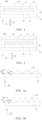
- FIG. 1 is a structural diagram of a first embodiment of a display device provided by an embodiment of this application.
- the display device 100 comprises a liquid crystal display panel 20, a backlight module 30 and a quantum dot composite film 10.
- the liquid crystal display panel 20 is arranged on a light emerging side of the backlight module 30.
- the quantum dot composite film 10 is arranged between the liquid crystal display panel 20 and the backlight module 30.
- the display device 100 may be a mobile terminal, such as a smart phone, a tablet computer, a notebook computer, etc..
- the display device 100 may also be a wearable terminal, such as a smart watch, a smart bracelet, smart glasses, and an augmented reality equipment, etc..
- the display device 100 may also be a fixed terminal, such as a desktop computer, a television and the like.
- the types of the liquid crystal display panel 20 comprise, but are not limited to, VA type, IPS type, TN type and the like.
- the quantum dot composite film 10 comprises a quantum dot film layer 11 and a plurality of first prism structures 12.
- the first prism structures 12 are arranged on a light emerging surface of the quantum dot film layer 11.
- the quantum dot film layer 11 comprises a composite film substrate and a plurality of quantum dots uniformly dispersed in the composite film substrate.
- the material of the composite film substrate comprises a transparent polymer material, and the transparent polymer material comprises one or more of polyester resin (PET), polymethyl methacrylate (PMMA) and polycarbonate (PC).
- the quantum dot comprises a luminescent core and an inorganic protective shell layer encapsulating the luminescent core.
- the plurality of quantum dots comprise red light quantum dots and green light quantum dots.
- the material of the luminescent core of the red light quantum dots comprises at least one of CdSe, Cd2SeTe and InAs, and the material of the luminescent core of the green light quantum dots comprises at least one of ZnCdSe2, InP and Cd2SSe.
- the material of the inorganic protective shell layer comprises one or more combinations of CdS, ZnSe, ZnCdS2, ZnS and ZnO.
- the material of the inorganic protective shell layer may further comprise high-stability composite quantum dots and perovskite quantum dots, etc..
- the high-stability composite quantum dots comprise hydrogel state quantum dot structures or CdSe-SiO2.
- the material of the first prism structure 12 comprises transparent polymer and inorganic particles.
- the inorganic particles are uniformly dispersed in the transparent polymer.
- the material of the transparent polymer comprises a combination of at least one or more of polymethyl methacrylate (PMMA), polycarbonate (PC), polyester resin (PET) or epoxy resin (EP), and the material of the inorganic particles comprise a combination of at least one or more of TiO2, BaSO4 and ZrO2.
- the transparent polymer material mixed with inorganic particles can be directly coated on the light emerging surface of the quantum dot film layer 11, and then the transparent polymer material is imprinted to form an uneven surface. After the transparent polymer material to be imprinted is cured, the first prism structures 12 can be formed on the surface of the quantum dot film layer 11.
- the quantum dot composite film 10 further comprises a reflective polarizer 13, and the reflective polarizer 13 is disposed on a side of the first prism structures 12 away from the quantum dot film layer 11.
- the reflective polarizer 13 is attached to the surface of the first prism structures 12 away from the quantum dot film layer 11 through the first transparent adhesive layer 14.
- the side of the quantum dot film layer 11 of the quantum dot composite film 10 away from the first prism structures 12 is attached to the side of the backlight module 30 facing the liquid crystal display panel 20.
- the thickness of the first transparent adhesive layer 14 is 4 ⁇ m.
- the thickness of the first transparent adhesive layer 14 is not limited to 4 ⁇ m, but can also be 2 ⁇ m, 3 ⁇ m, 5 ⁇ m, etc., and only needs to be greater than or equal to 2 ⁇ m, and less than or equal to 5 ⁇ m.
- the quantum dot composite film 10 is attached to the backlight module 30, and the liquid crystal display panel 20 and the frame area of the backlight module 30 are attached by the sealant 40. Therefore, it is not necessary to attach the reflective polarizer 13 to the liquid crystal display panel 20.
- the quantum dot composite film 10 By attaching the quantum dot composite film 10 to the backlight module 30, the light efficiency of the backlight module can be effectively improved, thereby enhancing the brightness of the display device.
- FIG. 2 is a schematic structural diagram of a second embodiment of a display device provided by an embodiment of this application.
- the reflective polarizer 13 is attached to the surface of the first prism structures 12 away from the quantum dot film layer 11 through the first transparent adhesive layer 14.
- the surface of the reflective polarizer 13 away from the first prism structures 12 is attached to the surface of the liquid crystal display panel 20 facing the backlight module 30 through the second transparent adhesive layer 15.
- the liquid crystal display panel 20 and the frame area of the backlight module 30 are attached by the sealant 40. While not affecting the bonding of the liquid crystal display panel 20 and the quantum dot composite film 10 through the second transparent adhesive layer 15, the quantum dot composite film 10 can also be bonded to the bottom of the liquid crystal display panel 20 to simplify the structure of the backlight module 30, and improve the viewing angle of the display device.
- the thickness of the second transparent adhesive layer 15 is 10 ⁇ m.
- the thickness of the second transparent adhesive layer 15 is not limited to 10 ⁇ m, but can also be 5 ⁇ m, 8 ⁇ m, 15 ⁇ m, 18 ⁇ m or 20 ⁇ m, and only needs to be greater than or equal to 5 ⁇ m, and less than or equal to 20 ⁇ m.
- both the first transparent adhesive layer 14 and the second transparent adhesive layer 15 can be any one of ultraviolet light sensitive adhesive, pressure sensitive adhesive or epoxy heat sensitive adhesive.
- at least one of the first transparent glue layer 14 and the second transparent glue layer 15 can also be replaced with a haze glue layer.
- At least one or more combination of diffusion particles such as TiO2, BaSO4, ZrO2, etc. can be added to the haze glue layer, to alleviate or avoid the problem of poor display, such as rainbow patterns or moire patterns, which may be caused by the interference phenomenon due to the adhesion of different material film layers.
- the cross section of the first prism structures 12 is a triangle or a trapezoid.
- the plurality of first prism structures 12 are distributed continuously or distributed at intervals on the light emerging surface of the quantum dot film layer 11.
- FIGS. 3a to 3d are cross-sectional structural diagrams of a first embodiment of a quantum dot composite film provided by an embodiment of this application.
- the cross section is a plane parallel to the short side direction y and the thickness direction z of the quantum dot composite film 10.
- the cross section of the first prism structure 12 in FIG. 3a is an isosceles triangle.
- the height h1 of the first prism structure 12 in the thickness direction z of the quantum dot composite film 10 is 20 ⁇ m.
- the bottom angle ⁇ 1 of the first prism structure 12 is 30° .
- the cross section of the first prism structure 12 in FIG. 3b is an isosceles triangle.
- the height h1 of the first prism structure 12 in the thickness direction a3 of the quantum dot composite film 10 is 25 ⁇ m.
- the bottom angle ⁇ 1 of the first prism structure 12 is 45° .
- the first prism structures 12 in FIGS. 3a and 3b are distributed continuously on the light emerging surface of the quantum dot film layer 11, and the bottom angles of adjacent first prism structures 12 are connected to each other.
- the cross section of the first prism structure 12 in FIG. 3c is an isosceles triangle.
- the height h1 of the first prism structure 12 in the thickness direction a3 of the quantum dot composite film 10 is 30 ⁇ m.
- the bottom angle ⁇ 1 of the first prism structure 12 is 70° .
- the first prism structures 12 in FIG. 3c are distributed at intervals on the light emerging surface of the quantum dot film layer 11, and the distance d1 between any two adjacent first prism structures 12 is 30 ⁇ m.
- the cross section of the first prism structure 12 in FIG. 3d is an isosceles trapezoid.
- the height h1 of the first prism structure 12 in the thickness direction z of the quantum dot composite film 10 is 30 ⁇ m.
- the bottom angle ⁇ 1 of the first prism structure 12 is 60° .
- the plurality of first prism structures 12 are distributed continuously on the light emerging surface of the quantum dot composite film 10.
- the cross section of the first prism structure 12 is not limited to the isosceles triangle or isosceles trapezoid in the aforesaid embodiments, and may also be a right-angled triangle, other non-isosceles triangle, a right-angled trapezoid or other non-isosceles trapezoid.
- the distance between any two adjacent first prism structures 12 is not limited to the foregoing 30 ⁇ m, but can also be 10 ⁇ m, 50 ⁇ m, 70 ⁇ m, or 100 ⁇ m, etc., and only needs to be greater than 0 ⁇ m, and less than or equal to 100 ⁇ m.
- the bottom angle ⁇ 1 of the first prism structure 12 is not limited to 30° , 45° , 60° or 70° in the aforesaid embodiments, but can also be 20° or 80° , and only needs to be greater than or equal to 20° , and less than or equal to 80° .
- FIG. 4 is a diagram of a three-dimensional structure of a first embodiment of a quantum dot composite film provided by an embodiment of this application.
- the length direction of the first prism structure 12 is parallel to the long side direction x of the quantum dot composite film 10.
- the width direction of the first prism structure 12 is parallel to the short side direction y of the quantum dot composite film 10.
- the plurality of first prism structures 12 are distributed continuously along the short side direction y of the quantum dot composite film 10.
- FIGS. 5a to 5c are diagrams of the arrangement direction of the first prism structures provided by an embodiment of this application.
- the length direction of the first prism structure 12 is parallel to the long side direction x of the quantum dot composite film 10.
- the length direction of the first prism structure 12 is perpendicular to the long side direction x of the quantum dot composite film 10.
- the length direction of the first prism structure 12 intersects with the long side direction x of the quantum dot composite film 10 to form a certain angle, which may be an acute angle or an obtuse angle.
- the isosceles triangle is illustrated as the cross section of the first prism structure 12.
- Several first prism structures 12 are designed as shown in Table 1.
- the height h1 of the first prism structure 12 is unified to 35 ⁇ m, and the respective on-axis brightnesses and 1/2 brightness viewing angles are analyzed through optical simulation.
- the results are shown in Table 1: Table 1.
- Simulation results of optical specifications for different designs of first prism structures Taper/° Space/ ⁇ m on-axis brightness/a.u. 1/2 brightness viewing angle/° control group 45 0 9.9 63.9 1 30 0 10 63.6 2 60 0 10.2 63.4 3 70 0 10.4 62.5 4 45 25 10.9 62.4 5 45 50 11.2 62.1 6 45 75 11.3 61.9
- the on-axis brightness of the display device gradually increases with a larger amplitude.
- the on-axis brightness of the display device is increased by about 14% compared to the control group, and the 1/2 brightness viewing angle is slightly reduced, but it remains above 60° on one side.
- FIG. 6 is a histogram of simulation results of the large viewing angle color shift of the first prism structure with different bottom angles according to an embodiment of this application.
- the bottom angle ⁇ 1 of the first prism structure 12 is increased to 60° , the deviations of the color dot y of 30° and 60° viewing angles is significantly reduced; when the bottom angle ⁇ 1 of the first prism structure 12 is increased to 70° , both the perspective color dots x and y of 30° and 60° viewing angles are significantly improved.
- FIG. 7 is a diagram of the light incidence-emergence relationship of the first prism structure with different bottom angles according to an embodiment of this application. Since when the bottom angle ⁇ 1 of the first prism structure 12 is increased to 70° , the first prism structure 12 refracts light from the small viewing angle (0 to 30° ) to the large viewing angle to emerge, and refracts light from the medium viewing angle (0 to 30° ) to the large viewing angle to emerge, and totally refracts light from the large viewing angle (above 50° ) back to the quantum dot film layer 11 for emerging twice. After the light of respective viewing angles is averaged, the difference of the R, G and B light pattern is reduced, so that the color shift phenomenon is improved.
- FIG. 8 is a schematic structural diagram of a third embodiment of a display device provided by an embodiment of this application.
- the structure of the display device shown in FIG. 8 is substantially the same as that of the display device shown in FIG. 1 , except that the quantum dot composite film 10 in the display device shown in FIG. 8 does not comprise the reflective polarizer 13, but comprises a first optical film layer 16.
- the first optical film layer 16 is disposed on a side of the first prism structures 12 away from the quantum dot film layer 11.
- the surface of the first optical film layer 16 away from the quantum dot film layer 11 comprises a plurality of second prism structures 160.
- the first optical film layer 16 is attached to the surface of the first prism structures 12 away from the quantum dot film layer 11 through the first transparent adhesive layer 14.
- the quantum dot film layer 11 may be attached to the surface of the backlight module 30 facing the liquid crystal display panel 20.
- FIG. 9 is a schematic structural diagram of a fourth embodiment of a display device provided by an embodiment of this application.
- the structure of the display device shown in FIG. 9 is substantially the same as that of the display device shown in FIG. 8 , except that the quantum dot film layer 11 in the display device shown in FIG. 9 is not attached to the surface of the backlight module 30 facing the liquid crystal display panel 20.
- the surface of the first optical film layer 16 facing the liquid crystal display panel 20 can be attached to the bottom surface of the liquid crystal display panel 20 through the second optical adhesive layer 15.
- the first prism structure 12 can form a plurality of air gaps between the quantum dot film layer 11 and the first optical film layer 16. After the light emerges from the first prism structure 12 on the light emerging surface of the quantum dot film layer 11, the first light collection and refraction will occur in the process of passing through the air gap and then entering the first optical film layer 16. Thus, the angle between the light entering the first optical film layer 16 and the thickness direction z of the quantum dot composite film 10 is reduced.
- the second prism structure 160 on the surface of the first optical film layer 16 When the light emerges from the second prism structure 160 on the surface of the first optical film layer 16, the second light collection and refraction occurs. Compared with the light in the first optical film layer 16, the angle between the light after emerging from the second prism structure 160 and the thickness direction z of the quantum dot composite film 10 is reduced, so that the emerging angle of the light is reduced. Accordingly, the amount of light emerged in the super-large viewing angle (>60° ) range can be reduced, and the amount of light emerged in the smaller viewing angle range can be increased. Then, the on-axis brightness of the display panel is improved, and the problem of light leakage of the display panel in the large viewing angle of the dark state is improved.
- the control experiments are established by using the quantum dot composite film particles in the display device shown in FIG. 8 or FIG. 9 .
- the quantum dot composite layer 10 of the experimental group comprises a quantum dot film layer 11, a first prism structure 12 and a first optical film layer 16.
- the quantum dot composite layer 10 of the control group only comprises the quantum dot film layer 11 and the first optical film layer 16.
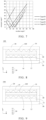
- FIG. 10 is a diagram of the comparison of the emerged light patterns of the experimental group and the control group of dots provided in an embodiment of this application.
- the viewing angle is between 0 and 60°
- the brightness of the experimental group and the control group are almost the same; when the viewing angle is greater than 60° , the brightness curve of the experimental group is significantly greater than the brightness curve of the control group, and the brightness of the experimental group is significantly lower than that of the control group.
- Table 2 optical specification data of experimental group and control group bright state dark state contrast control group 55.20nit 0.0243nit 2271 experimental group 78.18nit 0.0192nit 4071
- Table 2 is the optical specification data table of the experimental group and the control group provided in the embodiment of this application. Compared with the control group, the on-axis brightness of the experimental group is increased by 41.8%, the dark state brightness is decreased by 21.0%, and the contrast is increased by 79%.
- the cross section of the second prism structures 160 is a triangle or a trapezoid.
- the bottom angle of each second prism structure 160 is the same, and the bottom angle of the second prism structure 160 is greater than or equal to 20° , and less than or equal to 80° .
- FIGS. 11a to 11d are cross-sectional structural diagrams of a second embodiment of a quantum dot composite film provided by an embodiment of this application.
- the cross sections of the first prism structure 12 and the second prism structure 160 in FIG. 11a are both isosceles triangles.
- the plurality of first prism structures 12 are distributed continuously on the light emerging surface of the quantum dot film layer 11, and the plurality of second prism structures 160 are distributed continuously on the surface of the first optical film layer 16.
- the height h1 of the first prism structure 12 is 20 ⁇ m.
- the bottom angle ⁇ 1 of the first prism structure 12 is 30° .
- the height h2 of the second prism structure 160 is 20 ⁇ m.
- the bottom angle ⁇ 2 of the second prism structure 160 is 30° .
- the cross sections of the first prism structure 12 and the second prism structure 160 in FIG. 11b are both isosceles triangles.
- the plurality of first prism structures 12 are distributed at intervals on the light emerging surface of the quantum dot film layer 11, and the plurality of second prism structures 160 are distributed at intervals on the surface of the first optical film layer 16.
- the height h1 of the first prism structure 12 is 25 ⁇ m.
- the bottom angle ⁇ 1 of the first prism structure 12 is 60° .
- the distance d1 between any adjacent first prism structures 12 is 30 ⁇ m.
- the height h2 of the second prism structure 160 is 25 ⁇ m.
- the bottom angle ⁇ 2 of the second prism structure 160 is 45° .
- the distance d2 between any adjacent second prism structures 160 is 50 ⁇ m.
- the cross sections of the first prism structure 12 and the second prism structure 160 in FIG. 11c are both isosceles triangles.
- the plurality of first prism structures 12 are distributed continuously on the light emerging surface of the quantum dot film layer 11, and the plurality of second prism structures 160 are distributed continuously on the surface of the first optical film layer 16.
- the height h1 of the first prism structure 12 is 30 ⁇ m.
- the bottom angle ⁇ 1 of the first prism structure 12 is 45° .
- the height h2 of the second prism structure 160 is 30 ⁇ m.
- the bottom angle ⁇ 2 of the second prism structure 160 is 60° .
- the cross section of the first prism structure 12 is an isosceles triangle and the cross section of the second prism structure 160 is an isosceles trapezoid in FIG. 11b .
- the plurality of first prism structures 12 are distributed at intervals on the light emerging surface of the quantum dot film layer 11, and the plurality of second prism structures 160 are distributed continuously on the surface of the first optical film layer 16.
- the height h1 of the first prism structure 12 is 30 ⁇ m.
- the bottom angle ⁇ 1 of the first prism structure 12 is 70° .
- the distance between any adjacent first prism structures 12 is 25 ⁇ m.
- the height h2 of the second prism structure 160 is 30 ⁇ m.
- the bottom angle ⁇ 2 of the second prism structure 160 is 45° .
- the height h1 of the first prism structure 12 may also be 10 ⁇ m or 50 ⁇ m, etc., and only needs to be greater than or equal to 10 ⁇ m, and less than or equal to 50 ⁇ m.
- the height h2 of the second prism structure 160 may also be 10 ⁇ m or 50 ⁇ m, etc., and only needs to be greater than or equal to 10 ⁇ m, and less than or equal to 50 ⁇ m.
- the distance d2 between any two adjacent second prism structures 160 is not limited to the foregoing 25 ⁇ m or 50 ⁇ m in the aforesaid embodiments, but can also be 10 ⁇ m, 30 ⁇ m, 70 ⁇ m, or 100 ⁇ m, etc., and only needs to be greater than 0 ⁇ m, and less than or equal to 100 ⁇ m.
- the bottom angle ⁇ 2 of the second prism structure 160 can also be 20° , 50° or 80° , and only needs to be greater than or equal to 20° , and less than or equal to 80° .
- FIG. 12 is a diagram of the emerged light pattern corresponding to each experimental group in Table 3 provided by the embodiment of this application.
- the experimental groups 1 to 3 in FIG. 12 and Table 3 As shown in the experimental groups 1 to 3 in FIG. 12 and Table 3, as the bottom angle ⁇ 1 of the first prism structure 12 gradually increases, the on-axis brightness of the display device gradually increases, and the 1/2 brightness viewing angle basically remains unchanged. It can be seen that by changing the design of the first prism structure 12 on the light emerging surface of the quantum dot film layer 11, the energy efficiency of the display device can be increased by about 10%, and the 1/2 brightness viewing angle can be kept basically unchanged.
- the 1/2 brightness viewing angle gradually decreases, and the magnitude of the decrease is greater. It can be seen that by changing the design of the second prism structure 160, the one side 1/2 brightness viewing angle of the display device can be adjusted to be 40° to 60° . Therefore, the first prism structure 12 in the quantum dot composite film 10 mainly affects the energy efficiency of the display device, and the second prism structure 160 of the first optical film layer 16 mainly affects the viewing angle of the display device.
- the second prism structure 160 adopts a double Taper structure design, that is, the second prism structures 160 comprise a first sub-prism structure 161 and a second sub-prism structure 162.
- the second sub-prism structure 162 is interspersedly arranged between the first sub-prism structures 161 or arranged on a side of the first sub-prism structure 161.
- the bottom angle ⁇ 21 of the first sub-prism structure 161 is different from the bottom angle ⁇ 22 of the second sub-prism structure 162.
- the cross sections of the first sub-prism structure 161 and the second sub-prism structure 162 are the same.
- the height of the first sub-prism structure 161 and the height of the second sub-prism structure 162 in the thickness direction z of the quantum dot composite film 10 are the same, and the number of the first sub-prism structure 161 and the number of the second sub-prism structure 162 are the same.
- FIGS. 13a to 13d are cross-sectional structural diagrams of a third embodiment of a quantum dot composite film provided by an embodiment of this application.
- the cross sections of the first sub-prism structure 161 and the second sub-prism structure 162 are both isosceles triangles.
- the height are both 20 ⁇ m.
- the bottom angle ⁇ 21 of the first sub-prism structure 161 is 70° .
- the bottom angle ⁇ 22 of the second sub-prism structure 162 is 45° .
- the ratio of the number of the first sub-prism structure 161 to the number of the second sub-prism structure 162 is 1:1.
- the number of the first sub-prism structure 161 and the number of the second sub-prism structure 162 are different.
- the cross sections of the first sub-prism structure 161 and the second sub-prism structure 162 are both isosceles triangles.
- the height are both 20 ⁇ m.
- the bottom angle ⁇ 21 of the first sub-prism structure 161 is 60° .
- the bottom angle ⁇ 22 of the second sub-prism structure 162 is 45° .
- the ratio of the number of the first sub-prism structure 161 to the number of the second sub-prism structure 162 is 2:1.
- Two adjacent first sub-prism structures 161 are arranged between two adjacent second sub-prism structures 162.
- the ratio of the number of the first sub-prism structures 161 to the number of the second sub-prism structures 162 is not limited to the 2:1 in the foregoing embodiment, but may also be 3:1, 1:2, 1:3, etc.
- the cross sections of the first sub-prism structure 161 and the second sub-prism structure 162 are both isosceles trapezoids.
- the height are both 30 ⁇ m.
- the bottom angle ⁇ 21 of the first sub-prism structure 161 is 60° .
- the bottom angle ⁇ 22 of the second sub-prism structure 162 is 30° .
- the ratio of the number of the first sub-prism structure 161 to the number of the second sub-prism structure 162 is 1:1.
- the cross sections of the first sub-prism structure 161 and the second sub-prism structure 162 are different.
- the cross section of the first sub-prism structure 161 is an isosceles triangle and the second sub-prism structure 162 is an isosceles trapezoid.
- the heights of the first sub-prism structure 161 and the second sub-prism structure 162 are both 30 ⁇ m.
- the bottom angle ⁇ 21 of the first sub-prism structure 161 is 70° .
- the bottom angle ⁇ 22 of the second sub-prism structure 162 is 70° .
- the ratio of the number of the first sub-prism structure 161 to the number of the second sub-prism structure 162 is 1:1.
- the cross section of the first sub-prism structure 161 may also be an isosceles trapezoid
- the cross section of the second sub-prism structure 162 may also be an isosceles triangle.
- the bottom angle (taper) of the first sub-prism structure 161 may also be 45° , 50° , 80° , etc., and it only needs to be greater than or equal to 45° , and less than or equal to 80° .
- the bottom angle (taper) of the second sub-prism structure 162 may also be 10° , 20° , 40° , etc., and it only needs to be greater than or equal to 10° , and less than or equal to 45° .
- the height of the first sub-prism structure 161 may be the same as the height of the second sub-prism structure 162, or may be larger or smaller than the height of the second sub-prism structure 162.
- FIG. 14 is a diagram of the comparison of the emerged light patterns of the double prism structure provided by the embodiment of this application. Combining FIG. 14 and Table 4, it can be seen that in the experimental groups, the first sub-prism structure 161 and the second sub-prism structure 162 have different bottom angles, which can make the emerged light patterns of the emerged light show a stepwise change, to reduce the amount of light emerged from the large angle (40° to 60° ), thereby reducing the brightness of the specific viewing angle and reducing the problem of light leakage at the large viewing angle to improve the energy efficiency of the display device. At the same time, the amount of gamma shift of different gray levels under large viewing angles can be reduced, thereby improving the gamma shift under different gray levels.
- FIG. 15 is a diagram of a three-dimensional structure of the second embodiment of a quantum dot composite film provided by an embodiment of this application.
- the plurality of first prism structures 12 are distributed continuously along the first direction a1
- the plurality of second prism structures 160 are distributed continuously along the second direction a2.
- the first direction a1 and the second direction a2 are parallel, and both are parallel to the long side direction x of the quantum dot composite film 10 and perpendicular to the short side direction y of the quantum dot composite film 10.
- FIG. 16 is a diagram of another three-dimensional structure of the second embodiment of a quantum dot composite film provided by an embodiment of this application.
- the first prism structures 12 are distributed continuously along the first direction a1
- the second prism structures 160 are distributed continuously along the second direction a2.
- the first direction a1 is perpendicular to the second direction a2.
- the first direction a1 is parallel to the long side direction x of the quantum dot composite film 10.
- the second direction a2 is perpendicular to the long side direction x of the quantum dot composite film 10.
- the first direction a1 and the second direction a2 may not be perpendicular, but may intersect to form a certain angle, such as 10° , 20° ,45° , 60° , 70° or 80° .
- the bottom angle ⁇ 21 of the first sub-prism structure 161 may be 70°
- the bottom angle ⁇ 22 of the second sub-prism structure 162 may be 30°
- four control experimental groups were established.
- the refractive indexes of the first prism structures 12 in the four control experimental groups are different, which are 1.43, 1.50, 1.57 and 1.64 respectively.
- Table 5 shows optical specification data of respective experimental groups.
- FIG. 17 is a diagram of the comparison of the emerged light patterns of respective experimental groups provided by the embodiments of this application. Since the two-prisms structure of stacking the first prism structure 12 and the second prism structure 160 is designed, each of the four experimental groups possesses two inflection points in the light patterns of the emerged light. As the viewing angle increases, the brightness curve of each experimental group suddenly increases as passing the inflection point. In the four experimental groups, as the refractive index of the first prism structure 12 increases, the inflection point moves toward the direction of low angle. It can be seen that the larger the refractive index of the first prism structure 12, the smaller the viewing angle range generated by the inflection point. This is because as the refractive index of the first prism structure 12 increases, the refraction effect of the first prism structure 12 to the light is enhanced, and the emerging angle of the light becomes smaller.
- FIG. 18 is a histogram of the Gamma shift values of the 4 experimental groups in Table 5 at 102 gray scale and 20° viewing angle provided by the embodiments of this application.
- the No. 3 and No. 4 experimental groups can improve the gamma shift index to within the specification (that is, below 3%). In practical applications, materials with different refractive indices can be selected for the first prism structure 12 according to different optical specifications.
- the refractive index of the first prism structure 12 is 1.4.
- the refractive index of the first prism structure 12 is not limited to 1.4 in the foregoing embodiment, but can also be 1.3, 1.5, 1.6, or 1.7, etc., and only needs to be greater than or equal to 1.3, and less than or equal to 1.7.
- FIG. 19 is a schematic structural diagram of a fifth embodiment of a display device provided by an embodiment of this application.
- the structure of the display device shown in FIG. 19 is substantially the same as that of the display device shown in FIG. 8 , except that the quantum dot composite film 10 in the display device shown in FIG. 19 further comprises a reflective polarizer 13, and the reflective polarizer 13 is disposed on a side of the first optical film layer 16 away from the quantum dot film layer 11.
- the reflective polarizer 13 is attached to the surface of the first optical film layer 16 away from the quantum dot film layer 11 through the second transparent glue layer 15.
- FIG. 20 is a schematic structural diagram of a sixth embodiment of a display device provided by an embodiment of this application.
- the structure of the display device shown in FIG. 20 is substantially the same as that of the display device shown in FIG. 9 , except that the quantum dot composite film 10 in the display device shown in FIG. 20 comprises a quantum dot film layer 11, a first prism structure 12, a first optical film layer 16 and a reflective polarizer 13.
- the surface of the reflective polarizer 13 away from the first optical film layer 16 is attached to the surface of the liquid crystal display panel 20 close to the backlight module 30 through the haze glue layer 18.
- the use of the haze glue layer 18 can improve the problem of poor display, such as rainbow patterns or moire patterns, which may be caused by the interference phenomenon due to the adhesion of different material film layers.
- the embodiment of the present application provides a display device.
- the display device comprises a quantum dot composite film, a liquid crystal display panel and a backlight module.
- the quantum dot composite film comprises a quantum dot film layer, and a light emerging surface of the quantum dot film layer is provided with a plurality of first prism structures.
- the first prism structure is employed to adjust the emerging angle of light, so that more light emerges from smaller angles, thereby improving the front view brightness of the display device, and improving or avoiding the problem of light leakage of the display device in the large viewing angle of the dark state for improving the contrast of the display device.
Landscapes
- Physics & Mathematics (AREA)
- Nonlinear Science (AREA)
- General Physics & Mathematics (AREA)
- Optics & Photonics (AREA)
- Mathematical Physics (AREA)
- Chemical & Material Sciences (AREA)
- Crystallography & Structural Chemistry (AREA)
- Optical Elements Other Than Lenses (AREA)
- Liquid Crystal (AREA)
- Planar Illumination Modules (AREA)
Abstract
Description
- The present invention relates to a display technology field, and more particularly to a display device.
- At present, due to the excellent properties of quantum dot material (QD), such as high color purity and continuous adjustable spectrum, it has become the most excellent luminescent material in the 21st century, which can greatly improve the color performance of existing liquid crystal display (LCD) panels in the display color gamut, so its display applications have been widely studied in recent years.
- The existing quantum dot wide viewing angle display technology is to bond the quantum dot composite film to the prism, and utilize the property of the quantum dot to emerge light with a large viewing angle to improve the brightness of the liquid crystal display panel. However, due to the excessive diffusion of the viewing angle, this solution still emerges more light in the super-large viewing angle (>60° ) range, resulting in insufficient front-view brightness of the liquid crystal display panel, and the light leakage is serious and the contrast is obviously low in the large viewing angle of the dark state.
- In summary, the existing display device has the problems of insufficient formal brightness due to still more emerged light in the large viewing angle, and the light leakage in the large viewing angle of the dark state. Therefore, there is a need to provide a display device to improve this defect.
- The embodiment of the present application provides a display device to solve the problems of insufficient formal brightness in the existing display device due to still more emerged light in the large viewing angle, and the light leakage in the large viewing angle of the dark state.
- The embodiment of the present application provides a display device, comprising:
- a backlight module;
- a liquid crystal display panel arranged on a light emerging side of the backlight module; and
- a quantum dot composite film arranged between the liquid crystal display panel and the backlight module, wherein the quantum dot composite film comprises:
- a quantum dot film; and
- a plurality of first prism structures arranged on a light emerging surface of the quantum dot film layer.
- According to one embodiment of the present application, a cross section of the first prism structures is a triangle or a trapezoid.
- According to one embodiment of the present application, the plurality of first prism structures are distributed continuously or distributed at intervals along a first direction on the light emerging surface of the quantum dot film layer.
- According to one embodiment of the present application, the quantum dot composite film further comprises a reflective polarizer, and the reflective polarizer is disposed on a side of the first prism structures away from the quantum dot film layer.
- According to one embodiment of the present application, the quantum dot composite film further comprises a first optical film layer disposed on a side of the first prism structures away from the quantum dot film layer;
- wherein a surface of the first optical film layer away from the quantum dot film layer comprises a plurality of second prism structures.
- According to one embodiment of the present application, the plurality of second prism structures are distributed continuously or distributed at intervals along a second direction on a side of the first optical film layer away from the quantum dot film layer, and the first direction is parallel to or intersects with the second direction.
- According to one embodiment of the present application, a distance between adjacent second prism structures is greater than 0 µm, and less than or equal to 100 µ m.
- According to one embodiment of the present application, a cross section of the second prism structures is a triangle or a trapezoid.
- According to one embodiment of the present application, a bottom angle of each second prism structure is the same, and the bottom angle of the second prism structure is greater than or equal to 20° , and less than or equal to 80° .
- According to one embodiment of the present application, the second prism structures comprise a plurality of first sub-prism structures and a plurality of second sub-prism structures, and the second sub-prism structure is interspersedly arranged between the first sub-prism structures or arranged on a side of the first sub-prism structure;
wherein a bottom angle of the first sub-prism structure is different from a bottom angle of the second sub-prism structure; and/or a cross section of the first sub-prism structure is different from a cross section of the second sub-prism structure. - According to one embodiment of the present application, the bottom angle of the first sub-prism structure is greater than the bottom angle of the second sub-prism structure.
- According to one embodiment of the present application, the bottom angle of the first sub-prism structure is greater than 45° , and less than or equal to 80° , and the bottom angle of the second sub-prism structure is greater than or equal to 10° , and less than or equal to 45° .
- According to one embodiment of the present application, the reflective polarizer is arranged on a side of the first optical film layer away from the quantum dot film layer.
- According to one embodiment of the present application, a material of the first prism structure comprises transparent polymer and inorganic particles.
- According to one embodiment of the present application, the transparent polymer comprises at least one of polymethyl methacrylate, polycarbonate, polyester resin or epoxy resin, and the inorganic particles comprise at least one of TiO2, BaSO4 and ZrO2.
- According to one embodiment of the present application, a refractive index of the first prism structure is greater than or equal to 1.3, and less than or equal to 1.7.
- According to one embodiment of the present application, the quantum dot film layer comprises a composite film substrate and a plurality of quantum dots distributed in the composite film substrate;
wherein a material of the composite film substrate comprises transparent polymer. - According to one embodiment of the present application, a material of the transparent polymer comprises at least one of polymethyl methacrylate, polycarbonate, polyester resin or epoxy resin, and the quantum dot comprises a luminescent core and an inorganic protective shell layer encapsulating the luminescent core;
wherein a material of the inorganic protective shell layer comprises at least one of CdS, ZnSe, ZnCdS2, ZnS and ZnO. - According to one embodiment of the present application, the quantum dots comprise red light quantum dots and green light quantum dots;
wherein a material of the luminescent core of the red light quantum dots comprises at least one of CdSe, Cd2SeTe and InAs, and a material of the luminescent core of the green light quantum dots comprises at least one of ZnCdSe2, InP and Cd2SSe. - According to one embodiment of the present application, the quantum dot composite film is attached to a side of the liquid crystal display panel facing the backlight module; or the quantum dot composite film is attached to a side of the backlight module facing the liquid crystal display panel.
- The benefits of the embodiment of the present application are: The embodiment of the present application provides a display device. The display device comprises a quantum dot composite film, a liquid crystal display panel and a backlight module. The quantum dot composite film comprises a quantum dot film layer, and a light emerging surface of the quantum dot film layer is provided with a plurality of first prism structures. The refraction of light by the first prism structure is employed to reduce the emerging angle of light from the light emerging surface of the quantum dot film layer, thereby improving the front view brightness of the display device, and improving or avoiding the problem of light leakage of the display device in the large viewing angle of the dark state for improving the contrast of the display device.
- In order to more clearly illustrate the embodiments of the present disclosure or prior art, the following figures will be described in the embodiments are briefly introduced. It is obvious that the drawings are merely some embodiments of the present disclosure, those of ordinary skill in this field can obtain other figures according to these figures without paying the premise.
-
FIG. 1 is a structural diagram of a first embodiment of a display device provided by an embodiment of this application; -
FIG. 2 is a schematic structural diagram of a second embodiment of a display device provided by an embodiment of this application; -
FIGS. 3a to 3d are cross-sectional structural diagrams of a first embodiment of a quantum dot composite film provided by an embodiment of this application; -
FIG. 4 is a diagram of a three-dimensional structure of a first embodiment of a quantum dot composite film provided by an embodiment of this application; -
FIGS. 5a to 5c are diagrams of the arrangement direction of the first prism structures provided by an embodiment of this application; -
FIG. 6 is a histogram of simulation results of the large viewing angle color shift of the first prism structure with different bottom angles according to an embodiment of this application; -
FIG. 7 is a diagram of the light incidence-emergence relationship of the first prism structure with different bottom angles according to an embodiment of this application; -
FIG. 8 is a schematic structural diagram of a third embodiment of a display device provided by an embodiment of this application; -
FIG. 9 is a schematic structural diagram of a fourth embodiment of a display device provided by an embodiment of this application; -
FIG. 10 is a diagram of the comparison of the emerged light patterns of the experimental group and the control group of dots provided in an embodiment of this application; -
FIGS. 11a to 11d are cross-sectional structural diagrams of a second embodiment of a quantum dot composite film provided by an embodiment of this application; -
FIG. 12 is a diagram of the emerged light pattern corresponding to each experimental group in Table 3 provided by the embodiment of this application; -
FIGS. 13a to 13d are cross-sectional structural diagrams of a third embodiment of a quantum dot composite film provided by an embodiment of this application; -
FIG. 14 is a diagram of the comparison of the emerged light patterns of the double prism structure provided by the embodiment of this application; -
FIG. 15 is a diagram of a three-dimensional structure of the second embodiment of a quantum dot composite film provided by an embodiment of this application; -
FIG. 16 is a diagram of another three-dimensional structure of the second embodiment of a quantum dot composite film provided by an embodiment of this application; -
FIG. 17 is a diagram of the comparison of the emerged light patterns of respective experimental groups provided by the embodiments of this application; -
FIG. 18 is a histogram of the Gamma shift values of the 4 experimental groups in Table 5 at 102 gray scale and 20° viewing angle provided by the embodiments of this application; -
FIG. 19 is a schematic structural diagram of a fifth embodiment of a display device provided by an embodiment of this application; -
FIG. 20 is a schematic structural diagram of a sixth embodiment of a display device provided by an embodiment of this application. - The following descriptions for the respective embodiments are specific embodiments capable of being implemented for illustrations of the present application with referring to appended figures. The terms of up, down, front, rear, left, right, interior, exterior, side, etcetera in the present application are merely directions of referring to appended figures. Thus, the used directional terms are used to describe and understand the present application, but the present invention is not limited thereto. In the figure, units with similar structures are denoted by the same reference numerals.
- The present disclosure will be further described in detail with the accompanying drawings and the specific embodiments.
- The embodiment of this application provides a display device. As shown in
FIG. 1, FIG. 1 is a structural diagram of a first embodiment of a display device provided by an embodiment of this application. Thedisplay device 100 comprises a liquidcrystal display panel 20, abacklight module 30 and a quantum dotcomposite film 10. The liquidcrystal display panel 20 is arranged on a light emerging side of thebacklight module 30. The quantum dotcomposite film 10 is arranged between the liquidcrystal display panel 20 and thebacklight module 30. - In the embodiment of the present application, the
display device 100 may be a mobile terminal, such as a smart phone, a tablet computer, a notebook computer, etc.. Thedisplay device 100 may also be a wearable terminal, such as a smart watch, a smart bracelet, smart glasses, and an augmented reality equipment, etc.. Thedisplay device 100 may also be a fixed terminal, such as a desktop computer, a television and the like. - In the embodiment of the present application, the types of the liquid
crystal display panel 20 comprise, but are not limited to, VA type, IPS type, TN type and the like. - As shown in
FIG. 1 , the quantum dotcomposite film 10 comprises a quantumdot film layer 11 and a plurality offirst prism structures 12. Thefirst prism structures 12 are arranged on a light emerging surface of the quantumdot film layer 11. - The quantum
dot film layer 11 comprises a composite film substrate and a plurality of quantum dots uniformly dispersed in the composite film substrate. The material of the composite film substrate comprises a transparent polymer material, and the transparent polymer material comprises one or more of polyester resin (PET), polymethyl methacrylate (PMMA) and polycarbonate (PC). - The quantum dot comprises a luminescent core and an inorganic protective shell layer encapsulating the luminescent core. The plurality of quantum dots comprise red light quantum dots and green light quantum dots. The material of the luminescent core of the red light quantum dots comprises at least one of CdSe, Cd2SeTe and InAs, and the material of the luminescent core of the green light quantum dots comprises at least one of ZnCdSe2, InP and Cd2SSe.
- The material of the inorganic protective shell layer comprises one or more combinations of CdS, ZnSe, ZnCdS2, ZnS and ZnO. The material of the inorganic protective shell layer may further comprise high-stability composite quantum dots and perovskite quantum dots, etc.. The high-stability composite quantum dots comprise hydrogel state quantum dot structures or CdSe-SiO2.
- The material of the
first prism structure 12 comprises transparent polymer and inorganic particles. The inorganic particles are uniformly dispersed in the transparent polymer. The material of the transparent polymer comprises a combination of at least one or more of polymethyl methacrylate (PMMA), polycarbonate (PC), polyester resin (PET) or epoxy resin (EP), and the material of the inorganic particles comprise a combination of at least one or more of TiO2, BaSO4 and ZrO2. - In the embodiment of this application, the transparent polymer material mixed with inorganic particles can be directly coated on the light emerging surface of the quantum
dot film layer 11, and then the transparent polymer material is imprinted to form an uneven surface. After the transparent polymer material to be imprinted is cured, thefirst prism structures 12 can be formed on the surface of the quantumdot film layer 11. - Furthermore, the quantum dot
composite film 10 further comprises areflective polarizer 13, and thereflective polarizer 13 is disposed on a side of thefirst prism structures 12 away from the quantumdot film layer 11. - In one embodiment, as shown in
FIG. 1 , thereflective polarizer 13 is attached to the surface of thefirst prism structures 12 away from the quantumdot film layer 11 through the firsttransparent adhesive layer 14. The side of the quantumdot film layer 11 of the quantum dotcomposite film 10 away from thefirst prism structures 12 is attached to the side of thebacklight module 30 facing the liquidcrystal display panel 20. - Specifically, the thickness of the first
transparent adhesive layer 14 is 4 µm. In practical applications, the thickness of the firsttransparent adhesive layer 14 is not limited to 4 µm, but can also be 2 µm, 3 µm, 5 µm, etc., and only needs to be greater than or equal to 2 µm, and less than or equal to 5 µm. - In the embodiment shown in
FIG. 1 , the quantum dotcomposite film 10 is attached to thebacklight module 30, and the liquidcrystal display panel 20 and the frame area of thebacklight module 30 are attached by thesealant 40. Therefore, it is not necessary to attach thereflective polarizer 13 to the liquidcrystal display panel 20. By attaching the quantum dotcomposite film 10 to thebacklight module 30, the light efficiency of the backlight module can be effectively improved, thereby enhancing the brightness of the display device. - In one embodiment, as shown in
FIG. 2, FIG. 2 is a schematic structural diagram of a second embodiment of a display device provided by an embodiment of this application. Thereflective polarizer 13 is attached to the surface of thefirst prism structures 12 away from the quantumdot film layer 11 through the firsttransparent adhesive layer 14. The surface of thereflective polarizer 13 away from thefirst prism structures 12 is attached to the surface of the liquidcrystal display panel 20 facing thebacklight module 30 through the secondtransparent adhesive layer 15. - In the embodiment shown in
FIG. 2 , the liquidcrystal display panel 20 and the frame area of thebacklight module 30 are attached by thesealant 40. While not affecting the bonding of the liquidcrystal display panel 20 and the quantum dotcomposite film 10 through the secondtransparent adhesive layer 15, the quantum dotcomposite film 10 can also be bonded to the bottom of the liquidcrystal display panel 20 to simplify the structure of thebacklight module 30, and improve the viewing angle of the display device. - Specifically, the thickness of the second
transparent adhesive layer 15 is 10 µm. In practical applications, the thickness of the secondtransparent adhesive layer 15 is not limited to 10 µ m, but can also be 5 µm, 8 µm, 15 µ m, 18 µm or 20 µm, and only needs to be greater than or equal to 5 µm, and less than or equal to 20 µm. - Specifically, both the first
transparent adhesive layer 14 and the secondtransparent adhesive layer 15 can be any one of ultraviolet light sensitive adhesive, pressure sensitive adhesive or epoxy heat sensitive adhesive. In practical applications, at least one of the firsttransparent glue layer 14 and the secondtransparent glue layer 15 can also be replaced with a haze glue layer. At least one or more combination of diffusion particles such as TiO2, BaSO4, ZrO2, etc. can be added to the haze glue layer, to alleviate or avoid the problem of poor display, such as rainbow patterns or moire patterns, which may be caused by the interference phenomenon due to the adhesion of different material film layers. - Furthermore, the cross section of the
first prism structures 12 is a triangle or a trapezoid. The plurality offirst prism structures 12 are distributed continuously or distributed at intervals on the light emerging surface of the quantumdot film layer 11. - As shown in
FIGS. 3a to 3d, FIGS. 3a to 3d are cross-sectional structural diagrams of a first embodiment of a quantum dot composite film provided by an embodiment of this application. The cross section is a plane parallel to the short side direction y and the thickness direction z of the quantum dotcomposite film 10. The cross section of thefirst prism structure 12 inFIG. 3a is an isosceles triangle. The height h1 of thefirst prism structure 12 in the thickness direction z of the quantum dotcomposite film 10 is 20 µm. Thebottom angle α 1 of thefirst prism structure 12 is 30° . - The cross section of the
first prism structure 12 inFIG. 3b is an isosceles triangle. The height h1 of thefirst prism structure 12 in the thickness direction a3 of the quantum dotcomposite film 10 is 25 µm. Thebottom angle α 1 of thefirst prism structure 12 is 45° . - The
first prism structures 12 inFIGS. 3a and 3b are distributed continuously on the light emerging surface of the quantumdot film layer 11, and the bottom angles of adjacentfirst prism structures 12 are connected to each other. - The cross section of the
first prism structure 12 inFIG. 3c is an isosceles triangle. The height h1 of thefirst prism structure 12 in the thickness direction a3 of the quantum dotcomposite film 10 is 30 µm. Thebottom angle α 1 of thefirst prism structure 12 is 70° . Thefirst prism structures 12 inFIG. 3c are distributed at intervals on the light emerging surface of the quantumdot film layer 11, and the distance d1 between any two adjacentfirst prism structures 12 is 30 µm. - The cross section of the
first prism structure 12 inFIG. 3d is an isosceles trapezoid. The height h1 of thefirst prism structure 12 in the thickness direction z of the quantum dotcomposite film 10 is 30 µm. Thebottom angle α 1 of thefirst prism structure 12 is 60° . The plurality offirst prism structures 12 are distributed continuously on the light emerging surface of the quantum dotcomposite film 10. - In practical applications, the cross section of the
first prism structure 12 is not limited to the isosceles triangle or isosceles trapezoid in the aforesaid embodiments, and may also be a right-angled triangle, other non-isosceles triangle, a right-angled trapezoid or other non-isosceles trapezoid. - In practical applications, when the plurality of
first prism structures 12 are distributed at intervals on the surface of the quantumdot film layer 11, the distance between any two adjacentfirst prism structures 12 is not limited to the foregoing 30 µm, but can also be 10 µm, 50 µm, 70 µm, or 100 µm, etc., and only needs to be greater than 0 µm, and less than or equal to 100 µm. - In practical applications, the
bottom angle α 1 of thefirst prism structure 12 is not limited to 30° , 45° , 60° or 70° in the aforesaid embodiments, but can also be 20° or 80° , and only needs to be greater than or equal to 20° , and less than or equal to 80° . - As shown in
FIG. 4, FIG. 4 is a diagram of a three-dimensional structure of a first embodiment of a quantum dot composite film provided by an embodiment of this application. The length direction of thefirst prism structure 12 is parallel to the long side direction x of the quantum dotcomposite film 10. The width direction of thefirst prism structure 12 is parallel to the short side direction y of the quantum dotcomposite film 10. The plurality offirst prism structures 12 are distributed continuously along the short side direction y of the quantum dotcomposite film 10. - As shown in
FIGS. 5a to 5c, FIGS. 5a to 5c are diagrams of the arrangement direction of the first prism structures provided by an embodiment of this application. InFIG. 5a , the length direction of thefirst prism structure 12 is parallel to the long side direction x of the quantum dotcomposite film 10. InFIG. 5b , the length direction of thefirst prism structure 12 is perpendicular to the long side direction x of the quantum dotcomposite film 10. InFIG. 5c , the length direction of thefirst prism structure 12 intersects with the long side direction x of the quantum dotcomposite film 10 to form a certain angle, which may be an acute angle or an obtuse angle. - The isosceles triangle is illustrated as the cross section of the
first prism structure 12. Severalfirst prism structures 12 are designed as shown in Table 1. The height h1 of thefirst prism structure 12 is unified to 35 µm, and the respective on-axis brightnesses and 1/2 brightness viewing angles are analyzed through optical simulation. The results are shown in Table 1:Table 1. Simulation results of optical specifications for different designs of first prism structures Taper/° Space/µm on-axis brightness/a.u. 1/2 brightness viewing angle/° control group 45 0 9.9 63.9 1 30 0 10 63.6 2 60 0 10.2 63.4 3 70 0 10.4 62.5 4 45 25 10.9 62.4 5 45 50 11.2 62.1 6 45 75 11.3 61.9 - As shown in the first to third experiments in Table 1, as the angle of the bottom angle (taper) of the
first prism structure 12 gradually increases, the on-axis brightness of the display device gradually increases. Compared with the control group, in the third group of experiments, when the bottom angle is 70° , the on-axis brightness of the display device is increased by about 5%, and the 1/2 brightness viewing angle basically remains unchanged. - As shown in the fourth to sixth groups of experiments in Table 1, as the distance d1 between any adjacent
first prism structures 12 gradually increases, the on-axis brightness of the display device gradually increases with a larger amplitude. When the distance d1 between any adjacentfirst prism structures 12 gradually increases to 75 µm, the on-axis brightness of the display device is increased by about 14% compared to the control group, and the 1/2 brightness viewing angle is slightly reduced, but it remains above 60° on one side. - As shown in
FIG. 6, FIG. 6 is a histogram of simulation results of the large viewing angle color shift of the first prism structure with different bottom angles according to an embodiment of this application. When thebottom angle α 1 of thefirst prism structure 12 is increased to 60° , the deviations of the color dot y of 30° and 60° viewing angles is significantly reduced; when thebottom angle α 1 of thefirst prism structure 12 is increased to 70° , both the perspective color dots x and y of 30° and 60° viewing angles are significantly improved. - As shown in
FIG. 7, FIG. 7 is a diagram of the light incidence-emergence relationship of the first prism structure with different bottom angles according to an embodiment of this application. Since when thebottom angle α 1 of thefirst prism structure 12 is increased to 70° , thefirst prism structure 12 refracts light from the small viewing angle (0 to 30° ) to the large viewing angle to emerge, and refracts light from the medium viewing angle (0 to 30° ) to the large viewing angle to emerge, and totally refracts light from the large viewing angle (above 50° ) back to the quantumdot film layer 11 for emerging twice. After the light of respective viewing angles is averaged, the difference of the R, G and B light pattern is reduced, so that the color shift phenomenon is improved. - In one embodiment, as shown in
FIG. 8, FIG. 8 is a schematic structural diagram of a third embodiment of a display device provided by an embodiment of this application. The structure of the display device shown inFIG. 8 is substantially the same as that of the display device shown inFIG. 1 , except that the quantum dotcomposite film 10 in the display device shown inFIG. 8 does not comprise thereflective polarizer 13, but comprises a firstoptical film layer 16. The firstoptical film layer 16 is disposed on a side of thefirst prism structures 12 away from the quantumdot film layer 11. The surface of the firstoptical film layer 16 away from the quantumdot film layer 11 comprises a plurality ofsecond prism structures 160. - The first
optical film layer 16 is attached to the surface of thefirst prism structures 12 away from the quantumdot film layer 11 through the firsttransparent adhesive layer 14. The quantumdot film layer 11 may be attached to the surface of thebacklight module 30 facing the liquidcrystal display panel 20. - In one embodiment, as shown in
FIG. 9, FIG. 9 is a schematic structural diagram of a fourth embodiment of a display device provided by an embodiment of this application. The structure of the display device shown inFIG. 9 is substantially the same as that of the display device shown inFIG. 8 , except that the quantumdot film layer 11 in the display device shown inFIG. 9 is not attached to the surface of thebacklight module 30 facing the liquidcrystal display panel 20. The surface of the firstoptical film layer 16 facing the liquidcrystal display panel 20 can be attached to the bottom surface of the liquidcrystal display panel 20 through the secondoptical adhesive layer 15. - Specifically, as shown in
FIGS. 8 and 9 , thefirst prism structure 12 can form a plurality of air gaps between the quantumdot film layer 11 and the firstoptical film layer 16. After the light emerges from thefirst prism structure 12 on the light emerging surface of the quantumdot film layer 11, the first light collection and refraction will occur in the process of passing through the air gap and then entering the firstoptical film layer 16. Thus, the angle between the light entering the firstoptical film layer 16 and the thickness direction z of the quantum dotcomposite film 10 is reduced. - When the light emerges from the
second prism structure 160 on the surface of the firstoptical film layer 16, the second light collection and refraction occurs. Compared with the light in the firstoptical film layer 16, the angle between the light after emerging from thesecond prism structure 160 and the thickness direction z of the quantum dotcomposite film 10 is reduced, so that the emerging angle of the light is reduced. Accordingly, the amount of light emerged in the super-large viewing angle (>60° ) range can be reduced, and the amount of light emerged in the smaller viewing angle range can be increased. Then, the on-axis brightness of the display panel is improved, and the problem of light leakage of the display panel in the large viewing angle of the dark state is improved. - The control experiments are established by using the quantum dot composite film particles in the display device shown in
FIG. 8 or FIG. 9 . The quantum dotcomposite layer 10 of the experimental group comprises a quantumdot film layer 11, afirst prism structure 12 and a firstoptical film layer 16. The quantum dotcomposite layer 10 of the control group only comprises the quantumdot film layer 11 and the firstoptical film layer 16. - As shown in
FIG. 10, FIG. 10 is a diagram of the comparison of the emerged light patterns of the experimental group and the control group of dots provided in an embodiment of this application. When the viewing angle is between 0 and 60° , the brightness of the experimental group and the control group are almost the same; when the viewing angle is greater than 60° , the brightness curve of the experimental group is significantly greater than the brightness curve of the control group, and the brightness of the experimental group is significantly lower than that of the control group.Table 2. optical specification data of experimental group and control group bright state dark state contrast control group 55.20nit 0.0243nit 2271 experimental group 78.18nit 0.0192nit 4071 - As shown in Table 2, Table 2 is the optical specification data table of the experimental group and the control group provided in the embodiment of this application. Compared with the control group, the on-axis brightness of the experimental group is increased by 41.8%, the dark state brightness is decreased by 21.0%, and the contrast is increased by 79%.
- Combining
FIG. 10 and Table 2, it can be seen that adding thefirst prism structures 12 between the quantumdot film layer 11 and the firstoptical film layer 16 can effectively increase the on-axis brightness of the display device and improve the light leakage of the display device in the large viewing angle of the dark state, so as to improve the contrast of the display device. - Furthermore, the cross section of the
second prism structures 160 is a triangle or a trapezoid. The bottom angle of eachsecond prism structure 160 is the same, and the bottom angle of thesecond prism structure 160 is greater than or equal to 20° , and less than or equal to 80° . - As shown in
FIGS. 11a to 11d, FIGS. 11a to 11d are cross-sectional structural diagrams of a second embodiment of a quantum dot composite film provided by an embodiment of this application. - The cross sections of the
first prism structure 12 and thesecond prism structure 160 inFIG. 11a are both isosceles triangles. The plurality offirst prism structures 12 are distributed continuously on the light emerging surface of the quantumdot film layer 11, and the plurality ofsecond prism structures 160 are distributed continuously on the surface of the firstoptical film layer 16. The height h1 of thefirst prism structure 12 is 20 µm. Thebottom angle α 1 of thefirst prism structure 12 is 30° . The height h2 of thesecond prism structure 160 is 20 µm. Thebottom angle α 2 of thesecond prism structure 160 is 30° . - The cross sections of the
first prism structure 12 and thesecond prism structure 160 inFIG. 11b are both isosceles triangles. The plurality offirst prism structures 12 are distributed at intervals on the light emerging surface of the quantumdot film layer 11, and the plurality ofsecond prism structures 160 are distributed at intervals on the surface of the firstoptical film layer 16. The height h1 of thefirst prism structure 12 is 25 µm. Thebottom angle α 1 of thefirst prism structure 12 is 60° . The distance d1 between any adjacentfirst prism structures 12 is 30 µm. The height h2 of thesecond prism structure 160 is 25 µ m. Thebottom angle α 2 of thesecond prism structure 160 is 45° . The distance d2 between any adjacentsecond prism structures 160 is 50 µm. - The cross sections of the
first prism structure 12 and thesecond prism structure 160 inFIG. 11c are both isosceles triangles. The plurality offirst prism structures 12 are distributed continuously on the light emerging surface of the quantumdot film layer 11, and the plurality ofsecond prism structures 160 are distributed continuously on the surface of the firstoptical film layer 16. The height h1 of thefirst prism structure 12 is 30 µm. Thebottom angle α 1 of thefirst prism structure 12 is 45° . The height h2 of thesecond prism structure 160 is 30 µm. Thebottom angle α 2 of thesecond prism structure 160 is 60° . - The cross section of the
first prism structure 12 is an isosceles triangle and the cross section of thesecond prism structure 160 is an isosceles trapezoid inFIG. 11b . The plurality offirst prism structures 12 are distributed at intervals on the light emerging surface of the quantumdot film layer 11, and the plurality ofsecond prism structures 160 are distributed continuously on the surface of the first optical film layer 16.The height h1 of thefirst prism structure 12 is 30 µm. Thebottom angle α 1 of thefirst prism structure 12 is 70° . The distance between any adjacentfirst prism structures 12 is 25 µm. The height h2 of thesecond prism structure 160 is 30 µ m. Thebottom angle α 2 of thesecond prism structure 160 is 45° . - In practical applications, the height h1 of the
first prism structure 12 may also be 10 µm or 50 µm, etc., and only needs to be greater than or equal to 10 µm, and less than or equal to 50 µm. The height h2 of thesecond prism structure 160 may also be 10 µm or 50 µm, etc., and only needs to be greater than or equal to 10 µm, and less than or equal to 50 µm. - When the plurality of
second prism structures 160 are distributed at intervals, the distance d2 between any two adjacentsecond prism structures 160 is not limited to the foregoing 25 µm or 50 µm in the aforesaid embodiments, but can also be 10 µm, 30 µm, 70 µm, or 100 µm, etc., and only needs to be greater than 0 µm, and less than or equal to 100 µm. - In practical applications, the
bottom angle α 2 of thesecond prism structure 160 can also be 20° , 50° or 80° , and only needs to be greater than or equal to 20° , and less than or equal to 80° . - Six groups of experiments as shown in Table 3 are designed. Through optical simulation and experimental verification, the different prism structure designs of the quantum dot
composite film 10 possess different optical specifications.Table 3. design parameters and optical specifications of experimental groups experimental group first prism structure Taper/° second prism structure Taper/° on-axis brightness/a.u. 1/2 brightness viewing angle/° 1 30 45 12.34 55.3 2 45 45 13 55.2 3 60 45 13.6 54.4 4 45 30 12.2 61 5 45 45 13 55.2 6 45 60 12.72 45.8 - Combined with
Figure 12 and Table 3,FIG. 12 is a diagram of the emerged light pattern corresponding to each experimental group in Table 3 provided by the embodiment of this application. As shown in theexperimental groups 1 to 3 inFIG. 12 and Table 3, as thebottom angle α 1 of thefirst prism structure 12 gradually increases, the on-axis brightness of the display device gradually increases, and the 1/2 brightness viewing angle basically remains unchanged. It can be seen that by changing the design of thefirst prism structure 12 on the light emerging surface of the quantumdot film layer 11, the energy efficiency of the display device can be increased by about 10%, and the 1/2 brightness viewing angle can be kept basically unchanged. - As shown in the
experimental groups 4 to 6 inFIG. 12 and Table 3, as thebottom angle α 2 of thesecond prism structure 160 gradually increases, the 1/2 brightness viewing angle gradually decreases, and the magnitude of the decrease is greater. It can be seen that by changing the design of thesecond prism structure 160, the oneside 1/2 brightness viewing angle of the display device can be adjusted to be 40° to 60° . Therefore, thefirst prism structure 12 in the quantum dotcomposite film 10 mainly affects the energy efficiency of the display device, and thesecond prism structure 160 of the firstoptical film layer 16 mainly affects the viewing angle of the display device. - In one embodiment, the
second prism structure 160 adopts a double Taper structure design, that is, thesecond prism structures 160 comprise a firstsub-prism structure 161 and a secondsub-prism structure 162. The secondsub-prism structure 162 is interspersedly arranged between the firstsub-prism structures 161 or arranged on a side of the firstsub-prism structure 161. The bottom angle α 21 of the firstsub-prism structure 161 is different from the bottom angle α 22 of the secondsub-prism structure 162. - In an embodiment, the cross sections of the first
sub-prism structure 161 and the secondsub-prism structure 162 are the same. The height of the firstsub-prism structure 161 and the height of the secondsub-prism structure 162 in the thickness direction z of the quantum dotcomposite film 10 are the same, and the number of the firstsub-prism structure 161 and the number of the secondsub-prism structure 162 are the same. - As shown in
FIGS. 13a to 13d, FIGS. 13a to 13d are cross-sectional structural diagrams of a third embodiment of a quantum dot composite film provided by an embodiment of this application. InFIG. 13a , the cross sections of the firstsub-prism structure 161 and the secondsub-prism structure 162 are both isosceles triangles. The height are both 20 µ m. The bottom angle α 21 of the firstsub-prism structure 161 is 70° . The bottom angle α 22 of the secondsub-prism structure 162 is 45° . The ratio of the number of the firstsub-prism structure 161 to the number of the secondsub-prism structure 162 is 1:1. - In an embodiment, the number of the first
sub-prism structure 161 and the number of the secondsub-prism structure 162 are different. - As shown in
FIG. 13b , the cross sections of the firstsub-prism structure 161 and the secondsub-prism structure 162 are both isosceles triangles. The height are both 20 µm. The bottom angle α21 of the firstsub-prism structure 161 is 60° . The bottom angle α 22 of the secondsub-prism structure 162 is 45° . The ratio of the number of the firstsub-prism structure 161 to the number of the secondsub-prism structure 162 is 2:1. Two adjacent firstsub-prism structures 161 are arranged between two adjacent secondsub-prism structures 162. - In practical applications, the ratio of the number of the first
sub-prism structures 161 to the number of the secondsub-prism structures 162 is not limited to the 2:1 in the foregoing embodiment, but may also be 3:1, 1:2, 1:3, etc. - As shown in
FIG. 13c , the cross sections of the firstsub-prism structure 161 and the secondsub-prism structure 162 are both isosceles trapezoids. The height are both 30 µm. The bottom angle α 21 of the firstsub-prism structure 161 is 60° . The bottom angle α 22 of the secondsub-prism structure 162 is 30° . The ratio of the number of the firstsub-prism structure 161 to the number of the secondsub-prism structure 162 is 1:1. - In an embodiment, the cross sections of the first
sub-prism structure 161 and the secondsub-prism structure 162 are different. - As shown in
FIG. 13d , the cross section of the firstsub-prism structure 161 is an isosceles triangle and the secondsub-prism structure 162 is an isosceles trapezoid. The heights of the firstsub-prism structure 161 and the secondsub-prism structure 162 are both 30 µ m. The bottom angle α 21 of the firstsub-prism structure 161 is 70° . The bottom angle α 22 of the secondsub-prism structure 162 is 70° . The ratio of the number of the firstsub-prism structure 161 to the number of the secondsub-prism structure 162 is 1:1.In other embodiments, the cross section of the firstsub-prism structure 161 may also be an isosceles trapezoid, and the cross section of the secondsub-prism structure 162 may also be an isosceles triangle. - In practical applications, the bottom angle (taper) of the first
sub-prism structure 161 may also be 45° , 50° , 80° , etc., and it only needs to be greater than or equal to 45° , and less than or equal to 80° . The bottom angle (taper) of the secondsub-prism structure 162 may also be 10° , 20° , 40° , etc., and it only needs to be greater than or equal to 10° , and less than or equal to 45° . The height of the firstsub-prism structure 161 may be the same as the height of the secondsub-prism structure 162, or may be larger or smaller than the height of the secondsub-prism structure 162. - Eight groups of experiments as shown in Table 4 are designed. The cross sections and bottom angles of the first
sub-prism structure 161 and the secondsub-prism structure 162 in the control groups are the same, and the cross sections of the firstsub-prism structure 161 and the secondsub-prism structure 162 in the experimental groups are the same but the bottom angles are different.Table 4. Double Taper structure Gamma Shift improvement results control group experimental group gray scale 51 102 153 204 51 102 153 204 angle 20% 40% 60% 80% 20% 40% 60% 80% 0 0.00% 0.00% 0.00% 0.00% 0.00% 0.00% 0.00% 0.00% 10 0.66% 0.99% 0.66% -24.81% 0.63% 0.96% 0.69% -0.22% 20 2.60% 3.82% 2.51% -22.93% 2.15% 3.23% 2.28% -0.74% 30 5.62% 8.02% 5.10% -20.05% 4.37% 6.37% 4.37% -1.48% 40 9.56% 13.17% 8.07% -17.07% 6.15% 8.64% 5.74% -2.02% 50 13.39% 17.81 % 10.58% -13.42% 6.02% 8.17% 5.29% -1.86% 60 16.44% 21.24% 12.41 % -9.82% 4.91% 6.48% 4.14% -1.36% 70 15.97% 20.28% 11.84% -5.86% 3.48% 4.51% 2.88% -0.83% -
FIG. 14 is a diagram of the comparison of the emerged light patterns of the double prism structure provided by the embodiment of this application. CombiningFIG. 14 and Table 4, it can be seen that in the experimental groups, the firstsub-prism structure 161 and the secondsub-prism structure 162 have different bottom angles, which can make the emerged light patterns of the emerged light show a stepwise change, to reduce the amount of light emerged from the large angle (40° to 60° ), thereby reducing the brightness of the specific viewing angle and reducing the problem of light leakage at the large viewing angle to improve the energy efficiency of the display device. At the same time, the amount of gamma shift of different gray levels under large viewing angles can be reduced, thereby improving the gamma shift under different gray levels. - In one embodiment, as shown in
FIG. 15, FIG. 15 is a diagram of a three-dimensional structure of the second embodiment of a quantum dot composite film provided by an embodiment of this application. The plurality offirst prism structures 12 are distributed continuously along the first direction a1, and the plurality ofsecond prism structures 160 are distributed continuously along the second direction a2. The first direction a1 and the second direction a2 are parallel, and both are parallel to the long side direction x of the quantum dotcomposite film 10 and perpendicular to the short side direction y of the quantum dotcomposite film 10. - In one embodiment, as shown in
FIG. 16, FIG. 16 is a diagram of another three-dimensional structure of the second embodiment of a quantum dot composite film provided by an embodiment of this application. Thefirst prism structures 12 are distributed continuously along the first direction a1, thesecond prism structures 160 are distributed continuously along the second direction a2. The first direction a1 is perpendicular to the second direction a2. The first direction a1 is parallel to the long side direction x of the quantum dotcomposite film 10. The second direction a2 is perpendicular to the long side direction x of the quantum dotcomposite film 10. In practical applications, the first direction a1 and the second direction a2 may not be perpendicular, but may intersect to form a certain angle, such as 10° , 20° ,45° , 60° , 70° or 80° . - In one embodiment, the bottom angle α 21 of the first
sub-prism structure 161 may be 70° , and the bottom angle α 22 of the secondsub-prism structure 162 may be 30° . Based on the angles of the bottom angle α 21 of the firstsub-prism structure 161 and the bottom angle α 22 of the secondsub-prism structure 162 in this embodiment, four control experimental groups were established. The refractive indexes of thefirst prism structures 12 in the four control experimental groups are different, which are 1.43, 1.50, 1.57 and 1.64 respectively.Table 5.optical specification data of respective experimental groups experimental group α1 α2 refractive index viewing angle improvement range 1 70° 30° 1.43 40°~65° 2 70° 30° 1.50 35°~60° 3 70° 30° 1.57 25°~50° 4 70° 30° 1.64 20°~45° - As shown in Table. 5, Table 5 shows optical specification data of respective experimental groups. When the bottom angle of the
first prism structure 12 and the bottom angle of thesecond prism structure 160 remain constant, as the refractive index of thefirst prism structure 12 increases, the viewing angle improvement range gradually decreases. - As shown in
FIG. 17, FIG. 17 is a diagram of the comparison of the emerged light patterns of respective experimental groups provided by the embodiments of this application. Since the two-prisms structure of stacking thefirst prism structure 12 and thesecond prism structure 160 is designed, each of the four experimental groups possesses two inflection points in the light patterns of the emerged light. As the viewing angle increases, the brightness curve of each experimental group suddenly increases as passing the inflection point. In the four experimental groups, as the refractive index of thefirst prism structure 12 increases, the inflection point moves toward the direction of low angle. It can be seen that the larger the refractive index of thefirst prism structure 12, the smaller the viewing angle range generated by the inflection point. This is because as the refractive index of thefirst prism structure 12 increases, the refraction effect of thefirst prism structure 12 to the light is enhanced, and the emerging angle of the light becomes smaller. - As shown in
FIG. 18, FIG. 18 is a histogram of the Gamma shift values of the 4 experimental groups in Table 5 at 102 gray scale and 20° viewing angle provided by the embodiments of this application. With the increase of the refractive index of thefirst prism structure 12, the gamma shift value under this condition will decrease accordingly. The No. 3 and No. 4 experimental groups can improve the gamma shift index to within the specification (that is, below 3%). In practical applications, materials with different refractive indices can be selected for thefirst prism structure 12 according to different optical specifications. - In the embodiment of this application, the refractive index of the
first prism structure 12 is 1.4. In practical applications, the refractive index of thefirst prism structure 12 is not limited to 1.4 in the foregoing embodiment, but can also be 1.3, 1.5, 1.6, or 1.7, etc., and only needs to be greater than or equal to 1.3, and less than or equal to 1.7. - Furthermore, as shown in
FIG. 19, FIG. 19 is a schematic structural diagram of a fifth embodiment of a display device provided by an embodiment of this application. The structure of the display device shown inFIG. 19 is substantially the same as that of the display device shown inFIG. 8 , except that the quantum dotcomposite film 10 in the display device shown inFIG. 19 further comprises areflective polarizer 13, and thereflective polarizer 13 is disposed on a side of the firstoptical film layer 16 away from the quantumdot film layer 11. - The
reflective polarizer 13 is attached to the surface of the firstoptical film layer 16 away from the quantumdot film layer 11 through the secondtransparent glue layer 15. - In one embodiment, as shown in
FIG. 20, FIG. 20 is a schematic structural diagram of a sixth embodiment of a display device provided by an embodiment of this application. The structure of the display device shown inFIG. 20 is substantially the same as that of the display device shown inFIG. 9 , except that the quantum dotcomposite film 10 in the display device shown inFIG. 20 comprises a quantumdot film layer 11, afirst prism structure 12, a firstoptical film layer 16 and areflective polarizer 13. The surface of thereflective polarizer 13 away from the firstoptical film layer 16 is attached to the surface of the liquidcrystal display panel 20 close to thebacklight module 30 through thehaze glue layer 18. The use of thehaze glue layer 18 can improve the problem of poor display, such as rainbow patterns or moire patterns, which may be caused by the interference phenomenon due to the adhesion of different material film layers. - The benefits of the embodiment of the present application are: The embodiment of the present application provides a display device. The display device comprises a quantum dot composite film, a liquid crystal display panel and a backlight module. The quantum dot composite film comprises a quantum dot film layer, and a light emerging surface of the quantum dot film layer is provided with a plurality of first prism structures. The first prism structure is employed to adjust the emerging angle of light, so that more light emerges from smaller angles, thereby improving the front view brightness of the display device, and improving or avoiding the problem of light leakage of the display device in the large viewing angle of the dark state for improving the contrast of the display device.
- In summary, although the above preferred embodiments of the present application are disclosed, the foregoing preferred embodiments are not intended to limit the invention, those skilled in the art can make various kinds of alterations and modifications without departing from the spirit and scope of the present application. Thus, the scope of protection of the present application is defined by the scope of the claims.
Claims (20)
- A display device, comprising:a backlight module;a liquid crystal display panel arranged on a light emerging side of the backlight module; anda quantum dot composite film arranged between the liquid crystal display panel and the backlight module, wherein the quantum dot composite film comprises:a quantum dot film; anda plurality of first prism structures arranged on a light emerging surface of the quantum dot film layer.
- The display device according to claim 1, wherein a cross section of the first prism structures is a triangle or a trapezoid.
- The display device according to claim 1, wherein the plurality of first prism structures are distributed continuously or distributed at intervals along a first direction on the light emerging surface of the quantum dot film layer.
- The display device according to claim 3, wherein the quantum dot composite film further comprises a reflective polarizer, and the reflective polarizer is disposed on a side of the first prism structures away from the quantum dot film layer.
- The display device according to claim 4, wherein the quantum dot composite film further comprises a first optical film layer disposed on a side of the first prism structures away from the quantum dot film layer;
wherein a surface of the first optical film layer away from the quantum dot film layer comprises a plurality of second prism structures. - The display device according to claim 5, wherein the plurality of second prism structures are distributed continuously or distributed at intervals along a second direction on a side of the first optical film layer away from the quantum dot film layer, and the first direction is parallel to or intersects with the second direction.
- The display device according to claim 6, wherein a distance between adjacent second prism structures is greater than 0 µm, and less than or equal to 100 µm.
- The display device according to claim 5, wherein a cross section of the second prism structures is a triangle or a trapezoid.
- The display device according to claim 8, wherein a bottom angle of each second prism structure is the same, and the bottom angle of the second prism structure is greater than or equal to 20° , and less than or equal to 80° .
- The display device according to claim 8, wherein the second prism structures comprise a plurality of first sub-prism structures and a plurality of second sub-prism structures, and the second sub-prism structure is interspersedly arranged between the first sub-prism structures or arranged on a side of the first sub-prism structure;
wherein a bottom angle of the first sub-prism structure is different from a bottom angle of the second sub-prism structure; and/or a cross section of the first sub-prism structure is different from a cross section of the second sub-prism structure. - The display device according to claim 10, wherein the bottom angle of the first sub-prism structure is greater than the bottom angle of the second sub-prism structure.
- The display device according to claim 11, wherein the bottom angle of the first sub-prism structure is greater than 45° , and less than or equal to 80° , and the bottom angle of the second sub-prism structure is greater than or equal to 10° , and less than or equal to 45° .
- The display device according to claim 5, wherein the reflective polarizer is arranged on a side of the first optical film layer away from the quantum dot film layer.
- The display device according to claim 1, wherein a material of the first prism structure comprises transparent polymer and inorganic particles.
- The display device according to claim 14, wherein the transparent polymer comprises at least one of polymethyl methacrylate, polycarbonate, polyester resin or epoxy resin, and the inorganic particles comprise at least one of TiO2, BaSO4 and ZrO2.
- The display device according to claim 1, wherein a refractive index of the first prism structure is greater than or equal to 1.3, and less than or equal to 1.7.
- The display device according to claim 1, wherein the quantum dot film layer comprises a composite film substrate and a plurality of quantum dots distributed in the composite film substrate;
wherein a material of the composite film substrate comprises transparent polymer. - The display device according to claim 17, wherein a material of the transparent polymer comprises at least one of polymethyl methacrylate, polycarbonate, polyester resin or epoxy resin, and the quantum dot comprises a luminescent core and an inorganic protective shell layer encapsulating the luminescent core;
wherein a material of the inorganic protective shell layer comprises at least one of CdS, ZnSe, ZnCdS2, ZnS and ZnO. - The display device according to claim 18, wherein the quantum dots comprise red light quantum dots and green light quantum dots;
wherein a material of the luminescent core of the red light quantum dots comprises at least one of CdSe, Cd2SeTe and InAs, and a material of the luminescent core of the green light quantum dots comprises at least one of ZnCdSe2, InP and Cd2SSe. - The display device according to claim 1, wherein the quantum dot composite film is attached to a side of the liquid crystal display panel facing the backlight module; or the quantum dot composite film is attached to a side of the backlight module facing the liquid crystal display panel.
Applications Claiming Priority (2)
| Application Number | Priority Date | Filing Date | Title |
|---|---|---|---|
| CN202111408950.4A CN114035378B (en) | 2021-11-25 | 2021-11-25 | Display device |
| PCT/CN2021/136633 WO2023092668A1 (en) | 2021-11-25 | 2021-12-09 | Display device |
Publications (2)
| Publication Number | Publication Date |
|---|---|
| EP4439160A1 true EP4439160A1 (en) | 2024-10-02 |
| EP4439160A4 EP4439160A4 (en) | 2025-10-08 |
Family
ID=80138701
Family Applications (1)
| Application Number | Title | Priority Date | Filing Date |
|---|---|---|---|
| EP21827380.3A Pending EP4439160A4 (en) | 2021-11-25 | 2021-12-09 | Display device |
Country Status (5)
| Country | Link |
|---|---|
| US (1) | US12235544B2 (en) |
| EP (1) | EP4439160A4 (en) |
| JP (1) | JP7526214B2 (en) |
| CN (1) | CN114035378B (en) |
| WO (1) | WO2023092668A1 (en) |
Families Citing this family (2)
| Publication number | Priority date | Publication date | Assignee | Title |
|---|---|---|---|---|
| US12523907B2 (en) * | 2023-03-13 | 2026-01-13 | Meta Platforms Technologies, Llc | Wide color gamut enabled edge-lit BLU for high PPI VR-LCD display |
| US20260093112A1 (en) * | 2024-09-27 | 2026-04-02 | AUO Corporation | Display module and display system including the same |
Family Cites Families (27)
| Publication number | Priority date | Publication date | Assignee | Title |
|---|---|---|---|---|
| TWI317444B (en) * | 2004-09-03 | 2009-11-21 | Eternal Chemical Co Ltd | Optical film having high hardness and use thereof |
| CN100399146C (en) * | 2005-04-08 | 2008-07-02 | 友达光电股份有限公司 | Backlight module and brightness enhancement film thereof |
| JP5052797B2 (en) * | 2006-02-14 | 2012-10-17 | 古河電気工業株式会社 | Optical function sheet |
| JP5018371B2 (en) * | 2007-09-20 | 2012-09-05 | 凸版印刷株式会社 | Optical sheet, backlight unit and display device |
| JP5058000B2 (en) | 2008-01-15 | 2012-10-24 | 五洋紙工株式会社 | Light diffusing lens sheet, direct type backlight using the sheet, and liquid crystal television incorporating the backlight |
| JP2011123475A (en) * | 2009-11-16 | 2011-06-23 | Sumitomo Chemical Co Ltd | Polarizing plate, liquid crystal panel and liquid crystal display apparatus using the polarizing plate |
| JP2011150077A (en) * | 2010-01-20 | 2011-08-04 | Toppan Printing Co Ltd | Optical sheet, backlight unit and display device |
| KR101514657B1 (en) * | 2013-04-23 | 2015-05-04 | 주식회사 엘엠에스 | Organic-inorganic hybrid composition, optical member manufactured using the composition, and optical device |
| CN203413546U (en) * | 2013-06-28 | 2014-01-29 | 3M材料技术(广州)有限公司 | Optical film layer, backlight module and liquid crystal display device |
| KR102394030B1 (en) * | 2015-03-31 | 2022-05-06 | 삼성디스플레이 주식회사 | Prism plate, display device having the same, and method of manufacturing prism plate |
| KR102367759B1 (en) * | 2015-06-12 | 2022-02-28 | 삼성전자주식회사 | Back light unit and display apparutus comprising the same |
| JP6586805B2 (en) | 2015-07-14 | 2019-10-09 | 大日本印刷株式会社 | Edge light type backlight and liquid crystal display device |
| CN105137644B (en) * | 2015-09-23 | 2018-08-10 | 宁波激智科技股份有限公司 | One kind subtracting interferometric optical brightness enhancement film |
| CN108463528B (en) * | 2016-03-03 | 2019-03-15 | 东丽薄膜先端加工股份有限公司 | Laminated film |
| CN206594325U (en) * | 2017-02-20 | 2017-10-27 | 张家港康得新光电材料有限公司 | A kind of high printing opacity scratch-resistant brightness enhancement film |
| JP6886992B2 (en) | 2018-03-30 | 2021-06-16 | 恵和株式会社 | Light diffusing plate laminate, backlight unit, and liquid crystal display device |
| CN208999593U (en) * | 2018-09-26 | 2019-06-18 | 张家港康得新光电材料有限公司 | A kind of composite membrane |
| KR102591781B1 (en) | 2018-10-05 | 2023-10-23 | 삼성전자주식회사 | Display appartus |
| CN209514115U (en) | 2018-12-11 | 2019-10-18 | 宁波激智科技股份有限公司 | A kind of quantum dot composite light guide plate with multilayer prism structure |
| CN109445011A (en) * | 2018-12-17 | 2019-03-08 | 深圳市华星光电技术有限公司 | Quantum dot polaroid, display panel and display device |
| CN209148898U (en) * | 2018-12-25 | 2019-07-23 | 深圳市隆利科技股份有限公司 | If the diffusion barrier and backlight module and liquid crystal module and terminal device of prism structure |
| CN109739051A (en) * | 2019-02-21 | 2019-05-10 | 深圳市华星光电技术有限公司 | Quantum dot liquid crystal display |
| CN110174802A (en) * | 2019-06-03 | 2019-08-27 | 惠州市华星光电技术有限公司 | A kind of quantum dot LED backlight and preparation method thereof |
| CN210465918U (en) * | 2019-08-09 | 2020-05-05 | 广州市高浦特光电科技有限公司 | Brightness enhancement film |
| CN111458930A (en) * | 2020-03-06 | 2020-07-28 | Tcl华星光电技术有限公司 | Light-emitting composite film layer, backlight module and display device |
| CN212083715U (en) * | 2020-06-22 | 2020-12-04 | 深圳照东光控科技有限公司 | Microprism brightness enhancement film |
| CN113296312A (en) * | 2021-05-14 | 2021-08-24 | 惠州视维新技术有限公司 | Display device |
-
2021
- 2021-11-25 CN CN202111408950.4A patent/CN114035378B/en active Active
- 2021-12-09 JP JP2021576415A patent/JP7526214B2/en active Active
- 2021-12-09 WO PCT/CN2021/136633 patent/WO2023092668A1/en not_active Ceased
- 2021-12-09 US US17/620,671 patent/US12235544B2/en active Active
- 2021-12-09 EP EP21827380.3A patent/EP4439160A4/en active Pending
Also Published As
| Publication number | Publication date |
|---|---|
| JP2024501392A (en) | 2024-01-12 |
| CN114035378B (en) | 2023-06-27 |
| US20240045270A1 (en) | 2024-02-08 |
| JP7526214B2 (en) | 2024-07-31 |
| WO2023092668A1 (en) | 2023-06-01 |
| US12235544B2 (en) | 2025-02-25 |
| EP4439160A4 (en) | 2025-10-08 |
| CN114035378A (en) | 2022-02-11 |
Similar Documents
| Publication | Publication Date | Title |
|---|---|---|
| JP5237437B2 (en) | Display device | |
| US20110102721A1 (en) | Liquid crystal display device | |
| KR101605539B1 (en) | View angle-restricting sheet and flat panel display | |
| EP1143269B1 (en) | Optical path changing polarizer | |
| KR100662957B1 (en) | Masks, substrates with light reflecting films, methods of manufacturing display devices, display devices and electronic devices | |
| US20100068504A1 (en) | Multiple-coating particle and anti-glare film having the same | |
| US12235544B2 (en) | Display device | |
| KR102162846B1 (en) | Optical composite sheet and display apparatus comprising same | |
| US7321407B2 (en) | Reflector and liquid crystal display | |
| KR20030081089A (en) | Mask, substrate with light reflective film, method of forming light reflective film, and electro-optical display device and electronic apparatus | |
| KR100909427B1 (en) | Light control film | |
| KR102339785B1 (en) | Optical sheet and display apparatus comprising same | |
| KR20230127583A (en) | Liquid crystal display apparatus | |
| KR101087026B1 (en) | Optical Composite Film | |
| CN215415973U (en) | High-brightness peep-proof film | |
| KR100988764B1 (en) | Optical Composite Film | |
| CN109814185A (en) | A kind of micro- composite membrane of large scale and preparation method thereof | |
| EP4246193A1 (en) | Display synergistic film and display device | |
| CN220569045U (en) | Multilayer quantum dot composite film | |
| US20080013014A1 (en) | Optical hybrid film and manufacture thereof | |
| CN209947113U (en) | Large-size micro-permeable composite membrane | |
| CN117518600A (en) | Optical composite film, backlight module and display device | |
| CN117406488A (en) | Brightness enhancing film and preparation method thereof, backlight module | |
| TW202449425A (en) | Optical film and composite optical film | |
| US20230104988A1 (en) | Optical sheet and method for manufacturing optical sheet |
Legal Events
| Date | Code | Title | Description |
|---|---|---|---|
| STAA | Information on the status of an ep patent application or granted ep patent |
Free format text: STATUS: UNKNOWN |
|
| STAA | Information on the status of an ep patent application or granted ep patent |
Free format text: STATUS: THE INTERNATIONAL PUBLICATION HAS BEEN MADE |
|
| PUAI | Public reference made under article 153(3) epc to a published international application that has entered the european phase |
Free format text: ORIGINAL CODE: 0009012 |
|
| STAA | Information on the status of an ep patent application or granted ep patent |
Free format text: STATUS: REQUEST FOR EXAMINATION WAS MADE |
|
| 17P | Request for examination filed |
Effective date: 20211228 |
|
| AK | Designated contracting states |
Kind code of ref document: A1 Designated state(s): AL AT BE BG CH CY CZ DE DK EE ES FI FR GB GR HR HU IE IS IT LI LT LU LV MC MK MT NL NO PL PT RO RS SE SI SK SM TR |
|
| DAV | Request for validation of the european patent (deleted) | ||
| DAX | Request for extension of the european patent (deleted) | ||
| A4 | Supplementary search report drawn up and despatched |
Effective date: 20250909 |
|
| RIC1 | Information provided on ipc code assigned before grant |
Ipc: G02F 1/13357 20060101AFI20250903BHEP Ipc: G02F 1/1335 20060101ALI20250903BHEP |