EP4439026A1 - On-line dynamic resolution of time-based temperature estimation - Google Patents
On-line dynamic resolution of time-based temperature estimation Download PDFInfo
- Publication number
- EP4439026A1 EP4439026A1 EP23305442.8A EP23305442A EP4439026A1 EP 4439026 A1 EP4439026 A1 EP 4439026A1 EP 23305442 A EP23305442 A EP 23305442A EP 4439026 A1 EP4439026 A1 EP 4439026A1
- Authority
- EP
- European Patent Office
- Prior art keywords
- emu
- temperature
- value
- emulator circuit
- capacitor
- Prior art date
- Legal status (The legal status is an assumption and is not a legal conclusion. Google has not performed a legal analysis and makes no representation as to the accuracy of the status listed.)
- Granted
Links
Images




Classifications
-
- G—PHYSICS
- G01—MEASURING; TESTING
- G01K—MEASURING TEMPERATURE; MEASURING QUANTITY OF HEAT; THERMALLY-SENSITIVE ELEMENTS NOT OTHERWISE PROVIDED FOR
- G01K7/00—Measuring temperature based on the use of electric or magnetic elements directly sensitive to heat ; Power supply therefor, e.g. using thermoelectric elements
- G01K7/01—Measuring temperature based on the use of electric or magnetic elements directly sensitive to heat ; Power supply therefor, e.g. using thermoelectric elements using semiconducting elements having PN junctions
-
- G—PHYSICS
- G01—MEASURING; TESTING
- G01K—MEASURING TEMPERATURE; MEASURING QUANTITY OF HEAT; THERMALLY-SENSITIVE ELEMENTS NOT OTHERWISE PROVIDED FOR
- G01K15/00—Testing or calibrating of thermometers
- G01K15/005—Calibration
-
- G—PHYSICS
- G01—MEASURING; TESTING
- G01K—MEASURING TEMPERATURE; MEASURING QUANTITY OF HEAT; THERMALLY-SENSITIVE ELEMENTS NOT OTHERWISE PROVIDED FOR
- G01K2217/00—Temperature measurement using electric or magnetic components already present in the system to be measured
Definitions
- This disclosure pertains to the field of power semiconductor monitoring, and related calibration method, that are applicable during the operational life of such components.
- the free surface of a die is very small. To fix a sensor on it is difficult, and even impossible in some cases. The number of external connections is high, and the acquisition system is complex. To do it in laboratory conditions is very difficult. In real, industrial and operational situations, to use individual PN junction sensors is not realistic. In addition, sensors have to be integrated inside the power module packaging which means that the presence of sensors have to be initially planned during the conception of the module and to retrofit to the existing power modules is impossible.
- TSEP Temperature Sensitive Electrical Parameters
- ADC Analog-to-Digital Converter
- a TSEP of a transistor can be a time. More specifically, a TSEP of a transistor can be measured as a time duration relative to a detection threshold. A measurement of time may be a problem because of low temperature to time sensitivity.
- a simplest way is to monitor the passing of the temperature above a critical, safety-related, temperature value. This can be made with an analogue comparator comparing the TSEP value to a threshold value. Such a technic is described in EP 3 855 145 A1 . In this way, an ADC is not required but this limits the measurement to one specific temperature value. The specific temperature value is adjusted to correspond to the over-temperature of a specific power transistor.
- a critical, safety-related, temperature value Such a technic is described in EP 3 855 145 A1 .
- an ADC is not required but this limits the measurement to one specific temperature value.
- the specific temperature value is adjusted to correspond to the over-temperature of a specific power transistor.
- such a method presents the following limitations:
- This disclosure improves the situation.
- a power semi-conductor module comprising:
- a computer software comprising instructions to implement the method as defined here when the software is executed by a processor.
- a computer-readable non-transient recording medium on which a software is registered to implement the method as defined here when the software is executed by a processor.
- the resistance of said emulator circuit is tunable.
- the value of said resistance is set in such a way that the temperature estimation range amplitude is selected.
- the capacitor of said emulator circuit is tunable.
- the value of said capacitor is set in such a way that the temperature estimation range position is selected.
- the method further comprises:
- the method further comprises iteratively modifying the value of said resistance while the time duration t is fixed to a value close to zero and until the generated comparison signal corresponds to a situation wherein said voltage signal of said power transistor is equal to said voltage signal of said emulator circuit.
- the module further comprises:
- the word “power” is used in its general meaning of the technical field of energy conversion (power electronics).
- the solutions described hereinafter are made to be used during operational lifetime of the power semi-conductor modules under "normal” conditions, which means that it is not limited to the context of a laboratory or a test bench under ideal and controlled conditions like post-production quality control phases.
- the power semi-conductor module 1 comprises:
- the module 1 further comprises a time detector CHR.
- the time detector CHR is arranged to measure a time duration of the comparison signal V CMP .
- the time detector CHR can be a specific module by itself or can be a sub-module functionally integrated to the Comparator COMP.
- a pulse current is duplicated in two identical pulse currents.
- a pulse current from the current pulse source CPS is duplicated by the current copier CC, for example a "current mirror circuit".
- the aim is to inject the same current pulse, simultaneously, in the transistor TR and in the emulator circuit EMU.
- the first and second duplicated pulses currents are injected simultaneously respectively in a control electrode of the power transistor TR and in the emulator circuit EMU.
- the control electrode is the gate G of the transistor TR.
- the internal gate resistance of the transistor (present within the structure of the transistor) is used as a TSEP.
- the resulting voltages V ge and V emu are compared.
- the comparison is made by means of the comparator COMP between the gate-emitter voltage V ge of the transistor TR and the output voltage V emu of the emulator circuit EMU.
- V ge R g T j ⁇ I + t C g ⁇ I
- V emu R emu ⁇ I + t C emu ⁇ I
- I the current
- t the time
- R g (T j ) the gate resistor
- the gate resistor R g depends linearly on the temperature and can be described by the following equation [Math. 3].
- R g T j ⁇ R g ⁇ T j + 1 R g 0
- the comparison is binary: the output signal V CMP is equal to "1" when the transistor voltage is superior or equal to the emulator circuit voltage (V ge ⁇ V emu ), and "0" in the other cases (V ge ⁇ V emu ).
- V CMP 1
- the difference is analyzed with a binary value ("1" or "0") because the value of the difference is not relevant by itself. Only the duration of the sign of the difference is.
- the comparison of the two voltages can be made differently and can be analogic for example.
- the relation between time and temperature is independent of the value of the current injection.
- the method is robust to the imperfections of the current pulse source CPS and allows a good precision and a low-drift even if a low-cost current injection circuit is used.
- the temperature can be measured without additional ADC, considerably reducing the cost of the junction temperature T j measurement. Instead, a Time-to-Digital Converter (TDC) can be used, or even the time to digital conversion can be implemented in an FPGA, eventually in the same FPGA that generates control signals of a switch and other functions of the module 1.
- TDC Time-to-Digital Converter
- the measured duration ⁇ t is converted into a junction temperature T thanks to the linear relationship of the duration ⁇ t as a function of the temperature T. As it is represented on [ Fig. 4 ], the said relationship can be deduced from plurality of measurement at various temperatures T n .
- TDC Time-to-Digital Converter
- TDC7401ZAXRé has a resolution of 55ps.
- the temperature resolution can be expressed as a function of the TDC resolution with the following equation [Math. 5].
- Tj res TDC res C g ⁇ C emu C g ⁇ C emu ⁇ ⁇ R g
- the temperature-to-time resolution can easily be less than 1°C/ns, meaning that a TDC with a resolution of 55ps would allow to obtain a temperature resolution of less than 0.055°C.
- a current injection known in the art of 100mA and a resistance to temperature resolution of 0.013 ⁇ /°C in such a case, the temperature resolution is in the order of 0.5°C with a known 14bit ADC and a ⁇ 5V rail.
- the temperature resolution, and subsequent accuracy and precision can be much lower than state of the art methods.
- the output signal value of the comparator COMP can be either 0 or 1.
- two cases can be considered. The two cases are shown respectively on [ Fig. 5] and [Fig. 6 ].
- C g and R g are higher than C emu and R emu respectively.
- the output signal V CMP of the comparator COMP is equal to "1" and the length (duration) of the signal will be proportional to the temperature T j .
- C g and R g are lower than C emu and R emu respectively.
- the output signal V CMP of the comparator COMP is equal to "0" and the length (duration) of the signal will be proportional to the temperature T j .
- the emulator circuit EMU is tunable: the value of the resistance R emu can be set and the value of the capacitor C emu can be set (independently one with respect to the other). In various embodiment, only the resistance is tunable or only the capacitor is tunable. In other embodiments, the emulator circuit EMU is not tunable.
- Decreasing the capacitance C emu (during the operational life of the module 1) can be made by use of a laser trimmable chip capacitor built up as multilayer plate capacitors. Vaporizing the top layer with a laser decreases the capacitance by reducing the area of the top electrode. Depending on the industrial context, the resistor trimming process can be replaced by a capacitor trimming process when it is more convenient.
- the module 1 can further comprise a controller CONT.
- tunable capacitor and resistor can be digitally potentiometers controlled by the controller CONT, such as an FPGA.
- CONT such as an FPGA
- the component having the commercial reference "NCD2400MTR” can be used and give a range of 200pF with 512 discrete 355fF steps. If this range is not sufficient to cover full range of different device capacitance, the range can be increase by adding several bigger capacitances in parallel with one "NCD2400MTR" and controlled by the FPGA, as shown on [ Fig. 8 ].
- n-bit R-2R resistor ladder network controlled by an FPGA can be used. This allows to get 2n resistors steps directly tunable by the FPGA.
- digital potentiometer such as the component having the commercial reference "AD5258" with 64 resistor steps can be used.
- EMU emulator circuit
- CONT controller CONT
- TSEP of the transistor can be automatically calibrated using different algorithms. This allows to change (only) the transistor and keeping the temperature measurement operational.
- calibration procedures can be made regularly to balance any TSEP parameters variation.
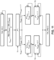
- [ Fig. 9 ], [ Fig. 10 ] and [ Fig. 11 ] are three examples of algorithms of calibration that can be used.
- the transistor is exposed at two different temperatures T1 and T2.
- the assembly is set at one first fixed temperature T1 and the time detection is set at one time t1.
- [ Fig. 11 ] is adapted to the two situations previously described when the resistance R g of the transistor is superior to the resistance R emu of the emulator circuit (R g > R emu ; see [ Fig. 5 ]), and when the resistance R g of the transistor is inferior to the resistance R emu of the emulator circuit (R g ⁇ R emu ; see [ Fig. 6 ]).
- the capacitance C emu is fixed at an intermediate value (for example a middle of the known range) and the temperature is fixed at one first known temperature T1. The time detection is gradually increased.
- the value of the resistance R emu of the emulator circuit with respect to the resistance R g of the transistor is less critical, and R emu may be a fixed resistor value instead of a tunable value.
- T1 or T2 One way to expose a transistor to a known temperature (T1 or T2) is to consider the ambient (heat-sink) temperature when said transistor has been in off-state for several minutes. Another way to expose the transistor to a known temperature is to consider the baseplate temperature when said transistor has been in off-state for several seconds.
- the temperature exposure can be performed ex-situ (i.e. outside the module), with a heat-plate, and/or in-situ, by considering the temperature at two different instants.
- an emulator circuit EMU having a tunable resistance R emu and a tunable capacitor C emu enables to calibrate the emulator circuit EMU in function of the transistor, for example only one time after the manufacturing/assembling process, periodically during the operational life of the module (for example during maintenance operations) or even during the "normal" operations of the modules.
- the range of temperature that can be estimated is related to the resistance R emu of the emulator circuit EMU while the amplitude (the sensitivity) of the temperature that can be deduced from the time t is related to the conductance C emu of the emulator circuit EMU.
- the solutions that we propose here enable to automatically and dynamically optimize the range and the resolution to each transistor and to each state of life (changing characteristics) of each transistor.
- one target of the calibration can be to cover a range of temperatures comprised between 125°C and 200°C (i.e. for protection).
- the target is to cover a range comprised between -40°C and 200°C (i.e. for counting the temperature cycles).
- the sensitivity can be optimized to be the highest.
- the performance of the junction temperature T J estimation circuit can be optimized to get the best precision in each range of temperatures.
- the junction temperature T J is estimated as being T J1 .
- the value T J1 is sufficiently centered in the measured range (curve "A”).
- the time-to-temperature sensitivity is increased, and the value T J1 is kept centered in the measured range (curve "B”).
- the time-to-temperature sensitivity is increased again, and the value T J1 is again kept centered in the measured range (curve "C”).
- the junction temperature T J changes (increases in the example) and is estimated as being T J2 .
- the junction temperature T J T J2 is not in the measurement range anymore (curve “C”).
- the time-to-temperature sensitivity is decreased (by modifying the value of the capacitor C emu of the emulator circuit): the temperature T J2 is in the measurement range but is not centered (Curve “D”).
- the temperature range is moved to center the estimated temperature T J2 (by modifying the value of the resistance R emu of the emulator circuit; Curve "E”)), and the sensitivity is increased (by modifying the value of the capacitor C emu of the emulator circuit; Curve “F”).
- the temperature range is maximized to know the approximate temperature range of the transistor.
- the controller applies the algorithm to set the value of R emu to focus on the temperature and C emu is adjusted to optimize the resolution.
- the algorithm readjusts R emu and C emu to focus the measurement on the new temperature.
- the time sensitivity can be increased. This allows to precisely measure a large range of temperature and over-passed the trade-off range/sensitivity by using different algorithms. Dynamic iterations are implemented to set the emulator circuit (R emu and C emu ). The range/sensitivity trade-off is over-passed. In other words, using several iterations, both a high measurement range and a high sensitivity can be reached.
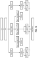
- [ Fig. 13 ] and [ Fig. 14 ] show examples of dynamic estimation/calibration algorithm implementations.
- the example of [ Fig. 13 ] is general and the example of [ Fig. 14 ] is more detailed to consider the two cases above described with respect to [ Fig. 5], [Fig. 6 ] and [ Fig. 11 ].
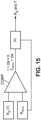
- dynamic estimation of the temperature by using tunable R emu and C emu parameters can also be done by fixing the time duration t close to "0" (to obtain R g (T) ; see [Math. 1]).
- This allows to determinate the temperature and the gate resistance R g (T) value by using a regulator, for example a Proportional, Integral one ("PI" on [ Fig. 15 ]).
- the value R g and the temperature T J can be estimated without measuring the time duration of the output signal of the comparator COMP.
- An aim of the previous description is to measure a junction temperature of a power transistor using the internal gate resistance R g as TSEP at high resolution, low circuit cost, low calibration effort, and with a high circuit genericity.
- calibrations can be made. Two equal currents are injected simultaneously through a control electrode of the transistor (generally the gate) and through an equivalent RC circuit called "emulator circuit".
- emulator circuit an equivalent RC circuit called "emulator circuit”.
- the voltages V ge and V emu are compared with an analogue comparator.
- the time duration (not the amplitude by itself) of the output signal of the comparator is linearly proportional to the temperature of the transistor. This allows to measure the junction temperature of the transistor without ADC.
- a controller for example an FPGA, it is possible to make calibration in situ for different components properties and to repeat the calibration during the operational life of the module to compensate deviation.
- modules according to the above can be used, for example, as power modules and inverters in automotive and powertrain technical fields, in factory automation, air-conditioning systems, HVDC and renewable energies.
Landscapes
- Physics & Mathematics (AREA)
- General Physics & Mathematics (AREA)
- Measurement Of Current Or Voltage (AREA)
- Measuring Temperature Or Quantity Of Heat (AREA)
Abstract
a. duplicating a pulse current;
b. injecting simultaneously
- a first duplicated pulse current to a control electrode of a power transistor of said power semi-conductor module, and
- a second duplicated pulse current to an emulator circuit comprising a resistance in series with a capacitor;
c. comparing a voltage signal of said power transistor and a voltage signal of said emulator circuit in such a way to generate a comparison signal;
d. in function of said comparison signal, measuring duration (Δt) of said voltage signal of said power transistor to reach the same value as said voltage signal of said emulator circuit;
e. converting said measured duration (Δt) into an estimated value of a junction temperature (TJ).
Description
- This disclosure pertains to the field of power semiconductor monitoring, and related calibration method, that are applicable during the operational life of such components.
- It is known to monitor temperature in power semiconductor devices/modules, like multichip power modules, for protection, condition and health monitoring because the temperature is one of the main failure origins. The datasheet of power semiconductor provides the maximum junction temperature where it can operate without thermal runaway and consequent catastrophic failure. Therefore, monitoring the junction temperature, or at least the maximum junction temperature measurement, is a great interest to ensure the safe operation of the device.
- Generally, the free surface of a die is very small. To fix a sensor on it is difficult, and even impossible in some cases. The number of external connections is high, and the acquisition system is complex. To do it in laboratory conditions is very difficult. In real, industrial and operational situations, to use individual PN junction sensors is not realistic. In addition, sensors have to be integrated inside the power module packaging which means that the presence of sensors have to be initially planned during the conception of the module and to retrofit to the existing power modules is impossible.
- Many Temperature Sensitive Electrical Parameters (TSEP) based methods and in-chip sensors for on-line junction temperature estimation on power semiconductor are known. This allows to have direct access to the junction temperature without the need of an external sensor. Typically, the measurement of the TSEP of a transistor is performed with an Analog-to-Digital Converter (ADC). The use of an ADC can be a limitation for low-cost systems since the resolution and sampling speed of the ADC directly relate to the quality of the temperature estimation. A TSEP of a transistor can be a time. More specifically, a TSEP of a transistor can be measured as a time duration relative to a detection threshold. A measurement of time may be a problem because of low temperature to time sensitivity. A simplest way is to monitor the passing of the temperature above a critical, safety-related, temperature value. This can be made with an analogue comparator comparing the TSEP value to a threshold value. Such a technic is described in
EP 3 855 145 A1 - Only one temperature is monitored. The predetermined temperature threshold is selected, generally according to a datasheet provided by the manufacturer.
- Monitoring multiple temperature values is possible but has a direct impact on the circuit and calibration complexity. Multiple temperatures can indeed be monitored by duplicating the monitoring circuit. The number of emulator components is thus multiplied, as well as the calibration effort.
- The Over-Temperature-Detection (OTD) circuit hardware needs to be specific for each monitored device. The TSEP characteristics being unique for each device, a calibration must be done for each OTD circuit. This limits the functionality of the OTD for one specific transistor.
- The OTD circuit is not modifiable, it cannot be adjusted during operation. A deviation of the TSEP during the mission profile of the device cannot be excluded which may alter the operation of the OTD, for example by modifying the measured temperature value.
- When the TSEP of a power transistor is the time, the time-to-temperature sensitivity is low. This will either lead to low precision/accuracy and/or require costly signal conditioning circuits.
- This disclosure improves the situation.
- It is proposed a measurement method for estimating junction temperatures of a power semi-conductor module comprising:
- a. duplicating a pulse current in two duplicated pulse currents;
- b. injecting simultaneously
- a first duplicated pulse current to a control electrode of a power transistor of said power semi-conductor module, and
- a second duplicated pulse current to an emulator circuit comprising a resistance in series with a capacitor;
- c. comparing a voltage signal of said power transistor and a voltage signal of said emulator circuit in such a way to generate a comparison signal;
- d. in function of said comparison signal, measuring duration of said voltage signal of said power transistor to reach the same value as said voltage signal of said emulator circuit;
- e. converting said measured duration into an estimated value of a junction temperature.
- In another aspect, it is proposed a power semi-conductor module comprising:
- at least one power transistor;
- a current pulse source that is provided through a control electrode of said power transistor;
- a current copier arranged to duplicate the current provided by the current pulse source;
- an emulator circuit comprising a resistance in series with a capacitor;
- a comparator arranged to compare a voltage signal of said power transistor and a voltage signal of said emulator circuit in such a way to generate a comparison signal.
- In another aspect, it is proposed a computer software comprising instructions to implement the method as defined here when the software is executed by a processor. In another aspect, it is proposed a computer-readable non-transient recording medium on which a software is registered to implement the method as defined here when the software is executed by a processor.
- The following features, can be optionally implemented, separately or in combination one with the others:
- The resistance of said emulator circuit is tunable. The value of said resistance is set in such a way that the temperature estimation range amplitude is selected. The capacitor of said emulator circuit is tunable. The value of said capacitor is set in such a way that the temperature estimation range position is selected.
- The method further comprises:
- f. modify the value of said resistance of the emulator circuit such that a corresponding temperature estimation range is modified and that the estimated value of a junction temperature get closer to the middle of the modified temperature estimation range;
- g1. if the estimated value of the junction temperature is sufficiently centered in the middle of the modified temperature estimation range according to predefined criteria, modify the value of said capacitor of the emulator circuit such that the sensitivity is increased;
- g2. if the estimated value of the junction temperature is not sufficiently centered in the middle of the modified temperature estimation range according to said predefined criteria, modify the value of said capacitor of the emulator circuit such that the sensitivity is decreased.
- The method further comprises iteratively modifying the value of said resistance while the time duration t is fixed to a value close to zero and until the generated comparison signal corresponds to a situation wherein said voltage signal of said power transistor is equal to said voltage signal of said emulator circuit.
- The module further comprises:
- a controller arranged to tune said resistance and/or said capacitor.
- Other features, details and advantages will be shown in the following detailed description and on the figures, on which:
-
Fig. 1
[Fig. 1 ] is a schematic view of a module according to some embodiments. -
Fig. 2
[Fig. 2 ] is a graphical representation of the measured output voltages during a current pulse and a corresponding comparison signal. -
Fig. 3
[Fig. 3 ] is a graphical representation of the measured output voltages during a current pulse and a corresponding comparison signal. -
Fig. 4
[Fig. 4 ] is a graphical representation of the linear relationship of the signal duration as a function of the temperature deduced from comparisons like in [Fig. 2] and [Fig. 3 ]. -
Fig. 5
[Fig. 5 ] is similar to [Fig. 2] or [Fig. 3 ] in a situation where Cg > Cemu. -
Fig. 6
[Fig. 6 ] is similar to [Fig. 2] or [Fig. 3 ] in a situation where Cg < Cemu. -
Fig. 7
[Fig. 7 ] is a graphic view of the temperature-to-time resolution as a function of the emulator capacitance. -
Fig. 8
[Fig. 8 ] is a schematic representation of a controller arrangement to tune an emulator circuit. -
Fig. 9
[Fig. 9 ] is a flowchart of an algorithm that can be executed during an embodiment. -
Fig. 10
[Fig. 10 ] is a flowchart of an algorithm that can be executed during an embodiment. -
Fig. 11
[Fig. 11 ] is a flowchart of an algorithm that can be executed during an embodiment. -
Fig. 12
[Fig. 12 ] is a graphical representation of a dynamic adaptation of an emulator circuit. -
Fig. 13
[Fig. 13 ] is a flowchart of an algorithm that can be executed during an embodiment. -
Fig. 14
[Fig. 14 ] is a flowchart of an algorithm that can be executed during an embodiment. -
Fig. 15
[Fig. 15 ] is a schematic representation of an embodiment of a dynamic adaptation of an emulator circuit. - Here, the word "power" is used in its general meaning of the technical field of energy conversion (power electronics). In addition, the solutions described hereinafter are made to be used during operational lifetime of the power semi-conductor modules under "normal" conditions, which means that it is not limited to the context of a laboratory or a test bench under ideal and controlled conditions like post-production quality control phases.
- It is now referred to [
Fig. 1 ] showing a modulepower semi-conductor module 1. Thepower semi-conductor module 1 comprises: - at least one power transistor TR;
- a current pulse source CPS that is provided through a control electrode G of said power transistor TR;
- a current copier CC arranged to duplicate the current provided by the current pulse source;
- an emulator circuit EMU comprising a resistance Remu in series with a capacitor Cemu,
- a comparator COMP arranged to compare a voltage signal Vge of said power transistor TR and a voltage signal Vemu of said emulator circuit EMU, here in such a way to generate a comparison signal VCMP.
- On [
Fig. 1 ], themodule 1 further comprises a time detector CHR. The time detector CHR is arranged to measure a time duration of the comparison signal VCMP. Structurally, the time detector CHR can be a specific module by itself or can be a sub-module functionally integrated to the Comparator COMP. - Examples of measurement method for estimating junction temperatures of a power semi-conductor module like the one shown on [
Fig. 1 ] will now be described. - In a first operation, a pulse current is duplicated in two identical pulse currents. In the example of [
Fig. 1 ], a pulse current from the current pulse source CPS is duplicated by the current copier CC, for example a "current mirror circuit". The aim is to inject the same current pulse, simultaneously, in the transistor TR and in the emulator circuit EMU. - In a second operation, the first and second duplicated pulses currents are injected simultaneously respectively in a control electrode of the power transistor TR and in the emulator circuit EMU. In the example of [
Fig. 1 ], the control electrode is the gate G of the transistor TR. Doing this, the internal gate resistance of the transistor (present within the structure of the transistor) is used as a TSEP. - In a third operation, the resulting voltages Vge and Vemu are compared. In the example of [
Fig. 1 ], the comparison is made by means of the comparator COMP between the gate-emitter voltage Vge of the transistor TR and the output voltage Vemu of the emulator circuit EMU. - The resulting voltages Vge and Vemu can be described respectively by the following equations [Math. 1] and [Math. 2].


where I is the current, t is the time and Rg(Tj) is the gate resistor. - The gate resistor Rg depends linearly on the temperature and can be described by the following equation [Math. 3].

- In the example, the comparison is binary: the output signal VCMP is equal to "1" when the transistor voltage is superior or equal to the emulator circuit voltage (Vge ≥ Vemu), and "0" in the other cases (Vge < Vemu). Thus, the time duration of the situation wherein the transistor voltage is superior or equal to the emulator circuit voltage (VCMP = 1) can be measured using equations [Math. 1] and [Math. 2], according to the following equation [Math. 4].

- Here, the difference is analyzed with a binary value ("1" or "0") because the value of the difference is not relevant by itself. Only the duration of the sign of the difference is. In various embodiments, the comparison of the two voltages can be made differently and can be analogic for example.
- The relation between time and temperature is independent of the value of the current injection. Thus, the method is robust to the imperfections of the current pulse source CPS and allows a good precision and a low-drift even if a low-cost current injection circuit is used. The temperature can be measured without additional ADC, considerably reducing the cost of the junction temperature Tj measurement. Instead, a Time-to-Digital Converter (TDC) can be used, or even the time to digital conversion can be implemented in an FPGA, eventually in the same FPGA that generates control signals of a switch and other functions of the
module 1. - The comparison of Vge and Vemu is graphically represented on [
Fig. 2], [Fig. 3] and [Fig. 4]. [Fig. 2 ] corresponds to the implementation under a first temperature T1 while [Fig. 3 ] corresponds to the implementation under a second temperature T2. - In a fourth operation, the measured duration Δt is converted into a junction temperature T thanks to the linear relationship of the duration Δt as a function of the temperature T. As it is represented on [
Fig. 4 ], the said relationship can be deduced from plurality of measurement at various temperatures Tn. - A Time-to-Digital Converter (TDC) can be used to implement the conversion, including TDC known by themselves. Some TDC offer resolutions better than 1ns. For example, the component having the commercial reference "TDC7401ZAXRé has a resolution of 55ps. The temperature resolution can be expressed as a function of the TDC resolution with the following equation [Math. 5].

- The temperature-to-time resolution can easily be less than 1°C/ns, meaning that a TDC with a resolution of 55ps would allow to obtain a temperature resolution of less than 0.055°C. To be convinced of the great resolution that can be reached by such a method, we should compare it to a current injection known in the art of 100mA and a resistance to temperature resolution of 0.013Ω/°C: in such a case, the temperature resolution is in the order of 0.5°C with a known 14bit ADC and a ±5V rail.
- The temperature resolution, and subsequent accuracy and precision can be much lower than state of the art methods.
- In the proposed example, the output signal value of the comparator COMP can be either 0 or 1. Depending on the value of Remu and Cemu, two cases can be considered. The two cases are shown respectively on [
Fig. 5] and [Fig. 6 ]. In a first case ([Fig. 5 ]), Cg and Rg are higher than Cemu and Remu respectively. The output signal VCMP of the comparator COMP is equal to "1" and the length (duration) of the signal will be proportional to the temperature Tj. In a second case ([Fig. 6 ]), Cg and Rg are lower than Cemu and Remu respectively. The output signal VCMP of the comparator COMP is equal to "0" and the length (duration) of the signal will be proportional to the temperature Tj. - In the examples, the emulator circuit EMU is tunable: the value of the resistance Remu can be set and the value of the capacitor Cemu can be set (independently one with respect to the other). In various embodiment, only the resistance is tunable or only the capacitor is tunable. In other embodiments, the emulator circuit EMU is not tunable.
- When the capacitor value Cemu is settable, it is thus possible to estimate the temperature only by setting Cemu independently of the value of Remu. When Remu < Rg (see [
Fig. 5 ]) and Remu > Rg (see [Fig. 6 ]), Cemu < Cg and Cemu > Cg, respectively. Thus, for example, a calibration process only of Cemu at the end of the manufacturing of themodule 1 can be performed, after the Tj estimation circuit is connected to the transistor TR. - For a given value of Remu:
- if no signal ("0") is detected at the output of the comparator COMP, Cemu must be increased;
- if only a positive signal ("1") is detected at the output of the comparator COMP, Cemu must be decreased.
- When the capacitor value Cemu is settable, it is thus possible to increase the temperature-to-time resolution by setting Cemu close to Cg. According to the equation [Math. 5], the closer the Cemu is and the higher the temperature-to-time resolution is. This is shown on [
Fig. 7 ]: the temperature-to-time resolution as a function of Cemu-Cg is plotted. On can see that the resolution increases for Cemu closer to Cg. - Decreasing the capacitance Cemu (during the operational life of the module 1) can be made by use of a laser trimmable chip capacitor built up as multilayer plate capacitors. Vaporizing the top layer with a laser decreases the capacitance by reducing the area of the top electrode. Depending on the industrial context, the resistor trimming process can be replaced by a capacitor trimming process when it is more convenient.
- In some embodiments with an emulator circuit EMU having a tunable resistance Remu and a tunable capacitor Cemu, further operations of calibration can be implemented. In such a case, the
module 1 can further comprise a controller CONT. - As an example, tunable capacitor and resistor can be digitally potentiometers controlled by the controller CONT, such as an FPGA. Only as an example, the component having the commercial reference "NCD2400MTR" can be used and give a range of 200pF with 512 discrete 355fF steps. If this range is not sufficient to cover full range of different device capacitance, the range can be increase by adding several bigger capacitances in parallel with one "NCD2400MTR" and controlled by the FPGA, as shown on [
Fig. 8 ]. - As a second example, a n-bit R-2R resistor ladder network controlled by an FPGA can be used. This allows to get 2n resistors steps directly tunable by the FPGA. As a third example, digital potentiometer such as the component having the commercial reference "AD5258" with 64 resistor steps can be used.
- A person skilled in the art would choose an emulator circuit EMU, including the controller CONT, adapted in function of the transistors to drive and the operational conditions, to adapt the range of capacitance. By using tunable capacitor and resistor, the TSEP of the transistor can be automatically calibrated using different algorithms. This allows to change (only) the transistor and keeping the temperature measurement operational. In addition, during the operational lifetime of the transistor (not only in laboratory conditions on a test bench), calibration procedures can be made regularly to balance any TSEP parameters variation.
- [
Fig. 9 ], [Fig. 10 ] and [Fig. 11 ] are three examples of algorithms of calibration that can be used. - In the example of [
Fig. 9 ], the transistor is exposed at two different temperatures T1 and T2. The capacitor Cemu and the resistor Remu are initially set at their lower values in order to obtain different output voltages between the transistor and the emulator circuit. This situation corresponds to VCMP = 1 if this algorithm of calibration is combined with the comparator COMP above described. The assembly is set at one first fixed temperature T1 and the time detection is set at one time t1. The resistance Remu is gradually increased until obtaining the same output voltages between the transistor and the emulator circuit (VCMP = 0). Then, the time detection is set at another time t2 and the capacitance Cemu is gradually increased until obtaining different output voltages between the transistor and the emulator circuit (VCMP = 1). Doing this, the time detection sensitivity is set. Finally, the temperature is fixed at a second temperature T2 and a time scan is performed until obtaining the same output voltages between the transistor and the emulator circuit (VCMP = 0). - The example of [
Fig. 9 ] enables to reduce the calibration effort because themodule 1 has to be exposed to only two different temperatures T1 and T2. A usual (cheap) FPGA is sufficient to do that. - In the example of [
Fig. 10 ], only the value of the capacitor Cemu is modified. The time detection is gradually increased to set the time detection corresponding to a first temperature T1. Then, the capacitor Cemu is gradually increased to fix the resolution of the detector. Finally, the temperature is fixed at a second temperature T2 and the time detection is gradually increased until obtaining different output voltages between the transistor and the emulator circuit (VCMP = 1). - The example of [
Fig. 10 ] enables to use a fixed (not tunable) resistance Remu. - The example of [
Fig. 11 ] is adapted to the two situations previously described when the resistance Rg of the transistor is superior to the resistance Remu of the emulator circuit (Rg > Remu ; see [Fig. 5 ]), and when the resistance Rg of the transistor is inferior to the resistance Remu of the emulator circuit (Rg < Remu ; see [Fig. 6 ]). Initially, the capacitance Cemu is fixed at an intermediate value (for example a middle of the known range) and the temperature is fixed at one first known temperature T1. The time detection is gradually increased. If the output voltages between the transistor and the emulator circuit was different and become equal (VCMP changes from 1 to 0), it means that Rg > Remu and we are in the case of [Fig. 5 ]. On the contrary, if output voltages between the transistor and the emulator circuit was equal and become different (VCMP changes from 0 to 1), it means that Rg < Remu and we are in case of [Fig. 6 ]. Then, the capacitance Cemu is decreased in the first case (Rg > Remu) and is increased in the second case (Rg < Remu) to set the time sensitivity. Then, the temperature is fixed at a second known temperature T2 and the time detection is gradually increased until obtaining the same output voltages between the transistor and the emulator circuit (VCMP = 0) in the first case (Rg > Remu), or until obtaining different output voltages between the transistor and the emulator circuit (VCMP = 1) in the second case (Rg < Remu). - In the example of [
Fig. 11 ] the value of the resistance Remu of the emulator circuit with respect to the resistance Rg of the transistor is less critical, and Remu may be a fixed resistor value instead of a tunable value. - One way to expose a transistor to a known temperature (T1 or T2) is to consider the ambient (heat-sink) temperature when said transistor has been in off-state for several minutes. Another way to expose the transistor to a known temperature is to consider the baseplate temperature when said transistor has been in off-state for several seconds. The temperature exposure can be performed ex-situ (i.e. outside the module), with a heat-plate, and/or in-situ, by considering the temperature at two different instants.
- As it is above explained, an emulator circuit EMU having a tunable resistance Remu and a tunable capacitor Cemu enables to calibrate the emulator circuit EMU in function of the transistor, for example only one time after the manufacturing/assembling process, periodically during the operational life of the module (for example during maintenance operations) or even during the "normal" operations of the modules. In the following, we will focus on solutions specifically adapted to be implemented dynamically, during the operational life of the module, to dynamically adapt the resolution of the temperature estimation when the temperature changes by mean of an embedded controller.
- The range of temperature that can be estimated is related to the resistance Remu of the emulator circuit EMU while the amplitude (the sensitivity) of the temperature that can be deduced from the time t is related to the conductance Cemu of the emulator circuit EMU. In other words, contrary to the prior art solutions where a definitive compromise must be made between a large amplitude and a high resolution, the solutions that we propose here enable to automatically and dynamically optimize the range and the resolution to each transistor and to each state of life (changing characteristics) of each transistor.
- As an example, one target of the calibration can be to cover a range of temperatures comprised between 125°C and 200°C (i.e. for protection). Alternatively, the target is to cover a range comprised between -40°C and 200°C (i.e. for counting the temperature cycles). For a specified temperature range, the sensitivity can be optimized to be the highest. The performance of the junction temperature TJ estimation circuit can be optimized to get the best precision in each range of temperatures.
- Since a junction temperature TJ has been estimated, the following operation can be implemented:
- f. modify the value of said resistance Remu of the emulator circuit EMU such that a corresponding temperature estimation range is modified and that the estimated value of a junction temperature TJ get closer to the middle of the modified temperature estimation range;
- g1. if the estimated value of the junction temperature TJ is sufficiently centered in the middle of the modified temperature estimation range according to predefined criteria, modify the value of said capacitor Cemu of the emulator circuit EMU such that the sensitivity is increased (and the range is reduced);
- g2. if the estimated value of the junction temperature TJ is not sufficiently centered in the middle of the modified temperature estimation range according to predefined criteria, modify the value of said capacitor Cemu of the emulator circuit EMU such that the sensitivity is decreased (and the range is increased).
- The above operations are graphically illustrated on [
Fig. 12 ]. In a first scenario (left part of [Fig. 12 ]), the junction temperature TJ is estimated as being TJ1. The value TJ1 is sufficiently centered in the measured range (curve "A"). Then, the time-to-temperature sensitivity is increased, and the value TJ1 is kept centered in the measured range (curve "B"). The time-to-temperature sensitivity is increased again, and the value TJ1 is again kept centered in the measured range (curve "C"). In a second scenario (right part of [Fig. 12 ]), the junction temperature TJ changes (increases in the example) and is estimated as being TJ2. The junction temperature TJ=TJ2 is not in the measurement range anymore (curve "C"). The time-to-temperature sensitivity is decreased (by modifying the value of the capacitor Cemu of the emulator circuit): the temperature TJ2 is in the measurement range but is not centered (Curve "D"). The temperature range is moved to center the estimated temperature TJ2 (by modifying the value of the resistance Remu of the emulator circuit; Curve "E")), and the sensitivity is increased (by modifying the value of the capacitor Cemu of the emulator circuit; Curve "F"). - In the example of [
Fig. 12 ], the temperature range is maximized to know the approximate temperature range of the transistor. Once the range of the temperature is known, the controller applies the algorithm to set the value of Remu to focus on the temperature and Cemu is adjusted to optimize the resolution. When the temperature of the transistor changes, the algorithm readjusts Remu and Cemu to focus the measurement on the new temperature. - To summarize, by approaching Cemu close to Cg, the time sensitivity can be increased. This allows to precisely measure a large range of temperature and over-passed the trade-off range/sensitivity by using different algorithms. Dynamic iterations are implemented to set the emulator circuit (Remu and Cemu). The range/sensitivity trade-off is over-passed. In other words, using several iterations, both a high measurement range and a high sensitivity can be reached.
- Only as examples, [
Fig. 13 ] and [Fig. 14 ] show examples of dynamic estimation/calibration algorithm implementations. The example of [Fig. 13 ] is general and the example of [Fig. 14 ] is more detailed to consider the two cases above described with respect to [Fig. 5], [Fig. 6 ] and [Fig. 11 ]. - In various embodiments, dynamic estimation of the temperature by using tunable Remu and Cemu parameters can also be done by fixing the time duration t close to "0" (to obtain Rg(T) ; see [Math. 1]). This method is shown on [
Fig. 15 ], where Cemu is constant and Remu is tuned until obtaining different output voltages between the transistor and the emulator circuit (VCMP = 1). This allows to determinate the temperature and the gate resistance Rg(T) value by using a regulator, for example a Proportional, Integral one ("PI" on [Fig. 15 ]). The value Rg and the temperature TJ can be estimated without measuring the time duration of the output signal of the comparator COMP. - An aim of the previous description is to measure a junction temperature of a power transistor using the internal gate resistance Rg as TSEP at high resolution, low circuit cost, low calibration effort, and with a high circuit genericity. Optionally, calibrations can be made. Two equal currents are injected simultaneously through a control electrode of the transistor (generally the gate) and through an equivalent RC circuit called "emulator circuit". In the embodiments wherein we want to do more than a measure/estimation on a specific transistor, we can further implement calibration steps by using tunable emulator circuit (the resistance Remu and/or the capacitance Cemu being tuned to be in the same range of respectively Rg and Cg of the transistor). The voltages Vge and Vemu are compared with an analogue comparator. The time duration (not the amplitude by itself) of the output signal of the comparator is linearly proportional to the temperature of the transistor. This allows to measure the junction temperature of the transistor without ADC. In addition, by using tunable resistor and capacitor controlled by a controller, for example an FPGA, it is possible to make calibration in situ for different components properties and to repeat the calibration during the operational life of the module to compensate deviation.
- Without limitation, modules according to the above can be used, for example, as power modules and inverters in automotive and powertrain technical fields, in factory automation, air-conditioning systems, HVDC and renewable energies.
- This disclosure is not limited to the methods, modules, components and computer software described here, which are only examples. The invention encompasses every alternative that a person skilled in the art would envisage when reading this text.
-
- 1: module
- CPS: current pulse source
- CC: current copier
- TR: transistor
- EMU: emulator circuit
- COMP: comparator
- CHR: time detector
- CONT: Controller.
Claims (8)
- A measurement method for estimating junction temperatures of a power semi-conductor module (1) comprising:a. duplicating a pulse current in two duplicated pulse currents;b. injecting simultaneously- a first duplicated pulse current to a control electrode (G) of a power transistor (TR) of said power semi-conductor module (1), and- a second duplicated pulse current to an emulator circuit (EMU) comprising a resistance (Remu) in series with a capacitor (Cemu);c. comparing a voltage signal (Vge) of said power transistor (TR) and a voltage signal (Vemu) of said emulator circuit (EMU) in such a way to generate a comparison signal (VCMP);d. in function of said comparison signal (VCMP), measuring duration (Δt) of said voltage signal (Vge) of said power transistor (TR) to reach the same value as said voltage signal (Vemu) of said emulator circuit (EMU);e. converting said measured duration (Δt) into an estimated value of a junction temperature (TJ).
- Method according to the preceding claim, wherein said resistance (Remu of said emulator circuit (EMU) is tunable,wherein the value of said resistance (Remu) is set in such a way that the temperature estimation range amplitude is selected, andwherein said capacitor (Cemu) of said emulator circuit (EMU) is tunable and wherein the value of said capacitor (Cemu) is set in such a way that the temperature estimation range position is selected.
- Method according to one of the preceding claims, further comprising:f. modify the value of said resistance (Remu) of the emulator circuit (EMU) such that a corresponding temperature estimation range is modified and that the estimated value of a junction temperature (TJ) get closer to the middle of the modified temperature estimation range;g1. if the estimated value of the junction temperature (TJ) is sufficiently centered in the middle of the modified temperature estimation range according to predefined criteria, modify the value of said capacitor (Cemu) of the emulator circuit (EMU) such that the sensitivity is increased;g2. if the estimated value of the junction temperature (TJ) is not sufficiently centered in the middle of the modified temperature estimation range according to said predefined criteria, modify the value of said capacitor (Cemu) of the emulator circuit (EMU) such that the sensitivity is decreased.
- Method according to one of claims 1 and 2, further comprising iteratively modifying the value of said resistance (Remu) while the time duration t is fixed to a value close to zero and until the generated comparison signal (VCMP) corresponds to a situation wherein said voltage signal (Vge) of said power transistor (TR) is equal to said voltage signal (Vemu) of said emulator circuit (EMU).
- A power semi-conductor module (1) comprising:- at least one power transistor (TR);- a current pulse source (CPS) that is provided through a control electrode (G) of said power transistor (TR);- a current copier (CC) arranged to duplicate the current provided by the current pulse source;- an emulator circuit (EMU) comprising a resistance (Remu) in series with a capacitor (Cemu);- a comparator (COMP) arranged to compare a voltage signal (Vge) of said power transistor (TR) and a voltage signal (Vemu) of said emulator circuit (EMU) in such a way to generate a comparison signal (VCMP).
- A power semi-conductor module (1) according to the preceding claim further comprising:- a controller (CONT) arranged to tune said resistance (Remu) and/or said capacitor (Cemu).
- Computer software comprising instructions to cause the module (1) of claims 5 or 6 to implement the method according to one of claims 1 to 4 when the software is executed by a processor.
- Computer-readable non-transient recording medium on which a software is registered to implement a method according to one of claims 1 to 4 when the software is executed by a processor.
Priority Applications (4)
| Application Number | Priority Date | Filing Date | Title |
|---|---|---|---|
| EP23305442.8A EP4439026B1 (en) | 2023-03-29 | 2023-03-29 | On-line dynamic resolution of time-based temperature estimation |
| PCT/JP2024/080001 WO2024204867A1 (en) | 2023-03-29 | 2024-01-12 | On-line dynamic resolution of time-based temperature estimation |
| JP2025549241A JP2026512240A (en) | 2023-03-29 | 2024-01-12 | Online dynamic resolution of time-based temperature estimation |
| CN202480006113.4A CN120883031A (en) | 2023-03-29 | 2024-01-12 | Online dynamic resolution for time-based temperature estimation |
Applications Claiming Priority (1)
| Application Number | Priority Date | Filing Date | Title |
|---|---|---|---|
| EP23305442.8A EP4439026B1 (en) | 2023-03-29 | 2023-03-29 | On-line dynamic resolution of time-based temperature estimation |
Publications (2)
| Publication Number | Publication Date |
|---|---|
| EP4439026A1 true EP4439026A1 (en) | 2024-10-02 |
| EP4439026B1 EP4439026B1 (en) | 2025-04-02 |
Family
ID=86226541
Family Applications (1)
| Application Number | Title | Priority Date | Filing Date |
|---|---|---|---|
| EP23305442.8A Active EP4439026B1 (en) | 2023-03-29 | 2023-03-29 | On-line dynamic resolution of time-based temperature estimation |
Country Status (4)
| Country | Link |
|---|---|
| EP (1) | EP4439026B1 (en) |
| JP (1) | JP2026512240A (en) |
| CN (1) | CN120883031A (en) |
| WO (1) | WO2024204867A1 (en) |
Citations (1)
| Publication number | Priority date | Publication date | Assignee | Title |
|---|---|---|---|---|
| EP3855145A1 (en) | 2020-01-21 | 2021-07-28 | Mitsubishi Electric R & D Centre Europe B.V. | Device for sensing an over-temperature of a power semiconductor device |
-
2023
- 2023-03-29 EP EP23305442.8A patent/EP4439026B1/en active Active
-
2024
- 2024-01-12 CN CN202480006113.4A patent/CN120883031A/en active Pending
- 2024-01-12 WO PCT/JP2024/080001 patent/WO2024204867A1/en not_active Ceased
- 2024-01-12 JP JP2025549241A patent/JP2026512240A/en active Pending
Patent Citations (1)
| Publication number | Priority date | Publication date | Assignee | Title |
|---|---|---|---|---|
| EP3855145A1 (en) | 2020-01-21 | 2021-07-28 | Mitsubishi Electric R & D Centre Europe B.V. | Device for sensing an over-temperature of a power semiconductor device |
Non-Patent Citations (1)
| Title |
|---|
| JULIO BRANDELERO ET AL: "On-line Virtual Junction Temperature Measurement via DC Gate Current Injection", CIPS 2018 - 10TH INTERNATIONAL CONFERENCE ON INTEGRATED POWER ELECTRONICS SYSTEMS, 20-22 MARCH 2018, STUTTGART, GERMANY, 5 July 2018 (2018-07-05), Berlin - Offenbach, XP055604490, ISBN: 978-3-8007-4540-1, Retrieved from the Internet <URL:https://ieeexplore.ieee.org/ielx7/8402817/8402818/08403170.pdf?tp=&arnumber=8403170&isnumber=8402818&ref=aHR0cHM6Ly9pZWVleHBsb3JlLmllZWUub3JnL2RvY3VtZW50Lzg0MDMxNzA=> [retrieved on 20190710] * |
Also Published As
| Publication number | Publication date |
|---|---|
| JP2026512240A (en) | 2026-04-15 |
| WO2024204867A1 (en) | 2024-10-03 |
| CN120883031A (en) | 2025-10-31 |
| EP4439026B1 (en) | 2025-04-02 |
Similar Documents
| Publication | Publication Date | Title |
|---|---|---|
| US11525740B2 (en) | Methods of measuring real-time junction temperature in silicon carbide power MOSFET devices using turn-on delay, related circuits, and computer program products | |
| Ma et al. | Modeling and characterization of frequency-domain thermal impedance for IGBT module through heat flow information | |
| EP3049779B1 (en) | Method and apparatus for determining an actual junction temperature of an igbt device | |
| US8602645B2 (en) | Temperature detection system | |
| US7341374B2 (en) | Temperature measurement circuit calibrated through shifting a conversion reference level | |
| Strauss et al. | Measuring the junction temperature of an IGBT using its threshold voltage as a temperature sensitive electrical parameter (TSEP) | |
| US7448797B2 (en) | Component arrangement and method for determining the temperature in a semiconductor component | |
| EP2757357A2 (en) | Systems and methods for an auto-ranging temperature sensor | |
| JP2008513766A (en) | Digital temperature sensor and its calibration | |
| US5970074A (en) | Method and apparatus for measuring threshold characteristic of semiconductor integrated circuit | |
| US9939476B2 (en) | Capacitance measurement | |
| CN118019965A (en) | Method and circuit arrangement for determining the barrier temperature of a semiconductor component having an insulated gate | |
| JP2019536408A (en) | Method for managing health of multi-die power module and multi-die health monitoring device | |
| EP4439026B1 (en) | On-line dynamic resolution of time-based temperature estimation | |
| EP4439025B1 (en) | High-resolution time-based junction temperature estimation and calibration | |
| US6456096B1 (en) | Monolithically compatible impedance measurement | |
| Austrup et al. | Diagnosing degradation in power modules using phase delay changes of electrical response | |
| US11489434B2 (en) | Power transducer including a rate of voltage change detection circuit | |
| US20250155294A1 (en) | Measurement method for estimating temperature of power semiconductor module | |
| US20100145652A1 (en) | Method for estimating the temperature in an internal combustion engine | |
| JP2023551344A (en) | Method and system for determining junction temperature of power semiconductors | |
| Kuojun et al. | A fast baseline and trigger level calibration method in digital oscilloscope | |
| WO2013045960A2 (en) | Procedure and device for measuring silicon temperature and over-temperature protection of a power insulated gate bipolar transistor | |
| Hambali et al. | Computer-based system for calibration of temperature transmitter using RTD | |
| US20240369423A1 (en) | Temperature measurement techniques for battery management circuits |
Legal Events
| Date | Code | Title | Description |
|---|---|---|---|
| PUAI | Public reference made under article 153(3) epc to a published international application that has entered the european phase |
Free format text: ORIGINAL CODE: 0009012 |
|
| STAA | Information on the status of an ep patent application or granted ep patent |
Free format text: STATUS: THE APPLICATION HAS BEEN PUBLISHED |
|
| AK | Designated contracting states |
Kind code of ref document: A1 Designated state(s): AL AT BE BG CH CY CZ DE DK EE ES FI FR GB GR HR HU IE IS IT LI LT LU LV MC ME MK MT NL NO PL PT RO RS SE SI SK SM TR |
|
| STAA | Information on the status of an ep patent application or granted ep patent |
Free format text: STATUS: REQUEST FOR EXAMINATION WAS MADE |
|
| 17P | Request for examination filed |
Effective date: 20241023 |
|
| RBV | Designated contracting states (corrected) |
Designated state(s): AL AT BE BG CH CY CZ DE DK EE ES FI FR GB GR HR HU IE IS IT LI LT LU LV MC ME MK MT NL NO PL PT RO RS SE SI SK SM TR |
|
| GRAP | Despatch of communication of intention to grant a patent |
Free format text: ORIGINAL CODE: EPIDOSNIGR1 |
|
| STAA | Information on the status of an ep patent application or granted ep patent |
Free format text: STATUS: GRANT OF PATENT IS INTENDED |
|
| INTG | Intention to grant announced |
Effective date: 20241212 |
|
| GRAS | Grant fee paid |
Free format text: ORIGINAL CODE: EPIDOSNIGR3 |
|
| GRAA | (expected) grant |
Free format text: ORIGINAL CODE: 0009210 |
|
| STAA | Information on the status of an ep patent application or granted ep patent |
Free format text: STATUS: THE PATENT HAS BEEN GRANTED |
|
| P01 | Opt-out of the competence of the unified patent court (upc) registered |
Free format text: CASE NUMBER: APP_4096/2025 Effective date: 20250124 |
|
| AK | Designated contracting states |
Kind code of ref document: B1 Designated state(s): AL AT BE BG CH CY CZ DE DK EE ES FI FR GB GR HR HU IE IS IT LI LT LU LV MC ME MK MT NL NO PL PT RO RS SE SI SK SM TR |
|
| REG | Reference to a national code |
Ref country code: GB Ref legal event code: FG4D |
|
| REG | Reference to a national code |
Ref country code: CH Ref legal event code: EP |
|
| REG | Reference to a national code |
Ref country code: IE Ref legal event code: FG4D |
|
| REG | Reference to a national code |
Ref country code: DE Ref legal event code: R096 Ref document number: 602023002732 Country of ref document: DE |
|
| REG | Reference to a national code |
Ref country code: NL Ref legal event code: MP Effective date: 20250402 |
|
| PG25 | Lapsed in a contracting state [announced via postgrant information from national office to epo] |
Ref country code: NL Free format text: LAPSE BECAUSE OF FAILURE TO SUBMIT A TRANSLATION OF THE DESCRIPTION OR TO PAY THE FEE WITHIN THE PRESCRIBED TIME-LIMIT Effective date: 20250402 |
|
| REG | Reference to a national code |
Ref country code: AT Ref legal event code: MK05 Ref document number: 1781687 Country of ref document: AT Kind code of ref document: T Effective date: 20250402 |
|
| PG25 | Lapsed in a contracting state [announced via postgrant information from national office to epo] |
Ref country code: PT Free format text: LAPSE BECAUSE OF FAILURE TO SUBMIT A TRANSLATION OF THE DESCRIPTION OR TO PAY THE FEE WITHIN THE PRESCRIBED TIME-LIMIT Effective date: 20250804 Ref country code: FI Free format text: LAPSE BECAUSE OF FAILURE TO SUBMIT A TRANSLATION OF THE DESCRIPTION OR TO PAY THE FEE WITHIN THE PRESCRIBED TIME-LIMIT Effective date: 20250402 Ref country code: ES Free format text: LAPSE BECAUSE OF FAILURE TO SUBMIT A TRANSLATION OF THE DESCRIPTION OR TO PAY THE FEE WITHIN THE PRESCRIBED TIME-LIMIT Effective date: 20250402 |
|
| REG | Reference to a national code |
Ref country code: LT Ref legal event code: MG9D |
|
| PG25 | Lapsed in a contracting state [announced via postgrant information from national office to epo] |
Ref country code: NO Free format text: LAPSE BECAUSE OF FAILURE TO SUBMIT A TRANSLATION OF THE DESCRIPTION OR TO PAY THE FEE WITHIN THE PRESCRIBED TIME-LIMIT Effective date: 20250702 Ref country code: GR Free format text: LAPSE BECAUSE OF FAILURE TO SUBMIT A TRANSLATION OF THE DESCRIPTION OR TO PAY THE FEE WITHIN THE PRESCRIBED TIME-LIMIT Effective date: 20250703 |
|
| PG25 | Lapsed in a contracting state [announced via postgrant information from national office to epo] |
Ref country code: PL Free format text: LAPSE BECAUSE OF FAILURE TO SUBMIT A TRANSLATION OF THE DESCRIPTION OR TO PAY THE FEE WITHIN THE PRESCRIBED TIME-LIMIT Effective date: 20250402 |
|
| PG25 | Lapsed in a contracting state [announced via postgrant information from national office to epo] |
Ref country code: BG Free format text: LAPSE BECAUSE OF FAILURE TO SUBMIT A TRANSLATION OF THE DESCRIPTION OR TO PAY THE FEE WITHIN THE PRESCRIBED TIME-LIMIT Effective date: 20250402 |
|
| PG25 | Lapsed in a contracting state [announced via postgrant information from national office to epo] |
Ref country code: HR Free format text: LAPSE BECAUSE OF FAILURE TO SUBMIT A TRANSLATION OF THE DESCRIPTION OR TO PAY THE FEE WITHIN THE PRESCRIBED TIME-LIMIT Effective date: 20250402 |
|
| PG25 | Lapsed in a contracting state [announced via postgrant information from national office to epo] |
Ref country code: AT Free format text: LAPSE BECAUSE OF FAILURE TO SUBMIT A TRANSLATION OF THE DESCRIPTION OR TO PAY THE FEE WITHIN THE PRESCRIBED TIME-LIMIT Effective date: 20250402 |
|
| PG25 | Lapsed in a contracting state [announced via postgrant information from national office to epo] |
Ref country code: RS Free format text: LAPSE BECAUSE OF FAILURE TO SUBMIT A TRANSLATION OF THE DESCRIPTION OR TO PAY THE FEE WITHIN THE PRESCRIBED TIME-LIMIT Effective date: 20250702 |
|
| PG25 | Lapsed in a contracting state [announced via postgrant information from national office to epo] |
Ref country code: IS Free format text: LAPSE BECAUSE OF FAILURE TO SUBMIT A TRANSLATION OF THE DESCRIPTION OR TO PAY THE FEE WITHIN THE PRESCRIBED TIME-LIMIT Effective date: 20250802 |
|
| PG25 | Lapsed in a contracting state [announced via postgrant information from national office to epo] |
Ref country code: LV Free format text: LAPSE BECAUSE OF FAILURE TO SUBMIT A TRANSLATION OF THE DESCRIPTION OR TO PAY THE FEE WITHIN THE PRESCRIBED TIME-LIMIT Effective date: 20250402 |
|
| REG | Reference to a national code |
Ref country code: DE Ref legal event code: R097 Ref document number: 602023002732 Country of ref document: DE |
|
| PG25 | Lapsed in a contracting state [announced via postgrant information from national office to epo] |
Ref country code: DK Free format text: LAPSE BECAUSE OF FAILURE TO SUBMIT A TRANSLATION OF THE DESCRIPTION OR TO PAY THE FEE WITHIN THE PRESCRIBED TIME-LIMIT Effective date: 20250402 Ref country code: SM Free format text: LAPSE BECAUSE OF FAILURE TO SUBMIT A TRANSLATION OF THE DESCRIPTION OR TO PAY THE FEE WITHIN THE PRESCRIBED TIME-LIMIT Effective date: 20250402 |
|
| PG25 | Lapsed in a contracting state [announced via postgrant information from national office to epo] |
Ref country code: CZ Free format text: LAPSE BECAUSE OF FAILURE TO SUBMIT A TRANSLATION OF THE DESCRIPTION OR TO PAY THE FEE WITHIN THE PRESCRIBED TIME-LIMIT Effective date: 20250402 |
|
| PG25 | Lapsed in a contracting state [announced via postgrant information from national office to epo] |
Ref country code: EE Free format text: LAPSE BECAUSE OF FAILURE TO SUBMIT A TRANSLATION OF THE DESCRIPTION OR TO PAY THE FEE WITHIN THE PRESCRIBED TIME-LIMIT Effective date: 20250402 |
|
| PG25 | Lapsed in a contracting state [announced via postgrant information from national office to epo] |
Ref country code: SK Free format text: LAPSE BECAUSE OF FAILURE TO SUBMIT A TRANSLATION OF THE DESCRIPTION OR TO PAY THE FEE WITHIN THE PRESCRIBED TIME-LIMIT Effective date: 20250402 |
|
| PG25 | Lapsed in a contracting state [announced via postgrant information from national office to epo] |
Ref country code: IT Free format text: LAPSE BECAUSE OF FAILURE TO SUBMIT A TRANSLATION OF THE DESCRIPTION OR TO PAY THE FEE WITHIN THE PRESCRIBED TIME-LIMIT Effective date: 20250402 |
|
| PLBE | No opposition filed within time limit |
Free format text: ORIGINAL CODE: 0009261 |
|
| STAA | Information on the status of an ep patent application or granted ep patent |
Free format text: STATUS: NO OPPOSITION FILED WITHIN TIME LIMIT |
|
| REG | Reference to a national code |
Ref country code: CH Ref legal event code: L10 Free format text: ST27 STATUS EVENT CODE: U-0-0-L10-L00 (AS PROVIDED BY THE NATIONAL OFFICE) Effective date: 20260211 |
|
| 26N | No opposition filed |
Effective date: 20260105 |
|
| PGFP | Annual fee paid to national office [announced via postgrant information from national office to epo] |
Ref country code: DE Payment date: 20260313 Year of fee payment: 4 |
|
| PGFP | Annual fee paid to national office [announced via postgrant information from national office to epo] |
Ref country code: FR Payment date: 20260223 Year of fee payment: 4 |