EP4439011A1 - Photonics gyroscope with broadband light source - Google Patents
Photonics gyroscope with broadband light source Download PDFInfo
- Publication number
- EP4439011A1 EP4439011A1 EP24161512.9A EP24161512A EP4439011A1 EP 4439011 A1 EP4439011 A1 EP 4439011A1 EP 24161512 A EP24161512 A EP 24161512A EP 4439011 A1 EP4439011 A1 EP 4439011A1
- Authority
- EP
- European Patent Office
- Prior art keywords
- waveguide
- photonics
- gyroscope
- resonator
- light source
- Prior art date
- Legal status (The legal status is an assumption and is not a legal conclusion. Google has not performed a legal analysis and makes no representation as to the accuracy of the status listed.)
- Pending
Links
Images

Classifications
-
- G—PHYSICS
- G01—MEASURING; TESTING
- G01C—MEASURING DISTANCES, LEVELS OR BEARINGS; SURVEYING; NAVIGATION; GYROSCOPIC INSTRUMENTS; PHOTOGRAMMETRY OR VIDEOGRAMMETRY
- G01C19/00—Gyroscopes; Turn-sensitive devices using vibrating masses; Turn-sensitive devices without moving masses; Measuring angular rate using gyroscopic effects
- G01C19/58—Turn-sensitive devices without moving masses
- G01C19/64—Gyrometers using the Sagnac effect, i.e. rotation-induced shifts between counter-rotating electromagnetic beams
- G01C19/72—Gyrometers using the Sagnac effect, i.e. rotation-induced shifts between counter-rotating electromagnetic beams with counter-rotating light beams in a passive ring, e.g. fibre laser gyrometers
- G01C19/727—Gyrometers using the Sagnac effect, i.e. rotation-induced shifts between counter-rotating electromagnetic beams with counter-rotating light beams in a passive ring, e.g. fibre laser gyrometers using a passive ring resonator
-
- G—PHYSICS
- G01—MEASURING; TESTING
- G01C—MEASURING DISTANCES, LEVELS OR BEARINGS; SURVEYING; NAVIGATION; GYROSCOPIC INSTRUMENTS; PHOTOGRAMMETRY OR VIDEOGRAMMETRY
- G01C19/00—Gyroscopes; Turn-sensitive devices using vibrating masses; Turn-sensitive devices without moving masses; Measuring angular rate using gyroscopic effects
- G01C19/58—Turn-sensitive devices without moving masses
- G01C19/64—Gyrometers using the Sagnac effect, i.e. rotation-induced shifts between counter-rotating electromagnetic beams
- G01C19/72—Gyrometers using the Sagnac effect, i.e. rotation-induced shifts between counter-rotating electromagnetic beams with counter-rotating light beams in a passive ring, e.g. fibre laser gyrometers
- G01C19/721—Details, e.g. optical or electronical details
- G01C19/722—Details, e.g. optical or electronical details of the mechanical construction
-
- H—ELECTRICITY
- H01—ELECTRIC ELEMENTS
- H01S—DEVICES USING THE PROCESS OF LIGHT AMPLIFICATION BY STIMULATED EMISSION OF RADIATION [LASER] TO AMPLIFY OR GENERATE LIGHT; DEVICES USING STIMULATED EMISSION OF ELECTROMAGNETIC RADIATION IN WAVE RANGES OTHER THAN OPTICAL
- H01S3/00—Lasers, i.e. devices using stimulated emission of electromagnetic radiation in the infrared, visible or ultraviolet wave range
- H01S3/005—Optical devices external to the laser cavity, specially adapted for lasers, e.g. for homogenisation of the beam or for manipulating laser pulses, e.g. pulse shaping
- H01S3/0071—Beam steering, e.g. whereby a mirror outside the cavity is present to change the beam direction
Definitions
- the resonant optical gyroscope often requires narrow linewidth lasers for rate interrogation.
- One or multiple narrow linewidth lasers can be used to lock to the cavity resonances in the gyroscope.
- the rotation rate is determined by comparing the resonance shift between clockwise (CW) and counter-clockwise (CCW) beam directions.
- This narrow linewidth gyroscope system is expensive and complicated.
- the system bias performance is limited by the Kerr effect.
- the Kerr effect is caused by the different phase shifts between counter propagating beams due to the self-phase modulation (SPM) and cross-phase modulation (XPM) and is more prominent with narrow linewidth lasers.
- a photonics gyroscope comprises a light source on a photonics chip, the light source configured to emit a light beam with a broadband spectrum; a waveguide resonator on the photonics chip, the waveguide resonator in optical communication with the light source; a reflective component on the photonics chip and in optical communication with the waveguide resonator; a first optical detector on the photonics chip and in optical communication with the waveguide resonator; a second optical detector on the photonics chip and operatively coupled to the light source; a relative intensity noise (RIN) servo loop coupled between an output of the second optical detector and an input of the light source; and a rate calculation unit configured to receive a signal output from the first optical detector, the rate calculation unit operative to calculate a rotation rate signal for the photonics gyroscope.
- RIN relative intensity noise
- the light beam from the light source is directed into the waveguide resonator such that the light beam propagates in a counterclockwise (CCW) direction as a CCW beam in the waveguide resonator.
- a beam portion of the CCW beam is coupled out of the waveguide resonator toward the reflective component and reflected back by the reflective component as a reflected beam that is optically coupled into the waveguide resonator such that the reflected beam propagates in a clockwise (CW) direction as a CW beam in the waveguide resonator.
- the CW beam is coupled out of the waveguide resonator and directed to the first optical detector, which is operative to detect a resonance frequency shift between the CW and CCW beams caused by rotation of the photonics gyroscope.
- the RIN servo loop is configured to stabilize an intensity of the light beam emitted from the light source such that a bias error and noise in the photonics gyroscope is reduced.
- Photonics gyroscopes that utilize a broadband light source are described herein.
- a photonics gyroscope with a broadband light source compares the intensity difference between clockwise (CW) and counterclockwise (CCW) beam transmissions.
- the optical power at each resonant peak is low; therefore, a typical gyroscope measurement based on one single resonance peak is limited by the shot noise.
- using the broadband light source covers a significant amount (N) of resonance peaks.
- the Angle Random Walk (ARW) will be reduced from the shot noise limited ARW by a factor of the square root of N.
- the bias due to the Kerr effect is greatly reduced due to the broadband light source.
- the photonics gyroscope with a broadband light source is based on an optical waveguide resonator, such as a waveguide ring resonator, and waveguide coupler arrangements.
- An on-chip broadband light source such as at least one superluminescent diode (SLD), emits a light beam that is split into two outputs via a coupler.
- SLD superluminescent diode
- a couple of SLDs can be combined together for broader bandwidth and higher power.
- the light beam in one output is used for a relative intensity noise (RIN) servo loop to stabilize the light source intensity, such that a bias error and noise in the photonics gyroscope is reduced.
- RIN relative intensity noise
- the light beam from the other output is launched into the waveguide resonator in a CCW direction.
- This CCW light beam represents the transmission spectrum of the waveguide resonator in the CCW direction.
- the CCW light beam is then phase modulated and reflected by a reflective component, such as a Bragg grating fabricated on a waveguide, such that the reflected beam is directed in the CW direction in the waveguide resonator.
- the rotation of the photonics gyroscope causes the resonance frequency shift between CW and CCW directions.
- the output intensity varies with the Sagnac frequency shift.
- the phase modulation and demodulation process converts the intensity output from a resonance peak to a linear output.
- the rotation rate magnitude and direction can be calculated from components of the demodulated signal, as well as using those components to suppress effects of the phase delay error between a phase modulator and the reflective component.
- the linewidth of waveguide resonator can be designed to be wider than the maximum Sagnac frequency shift.
- Prior approaches for resonant optical gyroscopes rely on narrow linewidth lasers and resonance locking loops for rate detection, which is complicated and expensive.
- the present approach reduces the complexity and cost by using the broadband light source and integrates all the optical gyroscope components on a single photonics chip.
- Using a broadband light source significantly reduces the bias instability due to the Kerr effect.
- the present integrated photonics gyroscopes can significantly reduce size, weight, and power (SWaP) when implemented as a navigation-grade gyroscope.
- SWaP size, weight, and power
- CMOS complementary metal-oxide-semiconductor
- CMOS complementary metal-oxide-semiconductor
- FIG 1 is a schematic illustration of an integrated photonics gyroscope 100 according to one embodiment.
- the photonics gyroscope 100 generally includes a waveguide resonator 110, such as a waveguide ring resonator, which is in optical communication with a broadband light source 112 through an optical path provided by a first waveguide arrangement 113.
- the optical components of photonics gyroscope 100 can be integrated on a single photonics chip 102.
- the waveguide resonator 110 can be formed to have a large polarization dependent loss, and to intrinsically support one polarization mode, which reduces bias error and instability in photonics gyroscope 100.
- waveguide resonator 110 can have a cavity linewidth of about 1 MHz.
- the light source 112 can be an amplified spontaneous emission (ASE) device, such as a superluminescent diode (SLD), which is configured to emit a light beam with a broadband spectrum.
- ASE amplified spontaneous emission
- SLD superluminescent diode
- two or more SLDs with different center wavelengths can be combined to increase the power and bandwidth of the ASE light.
- the first waveguide arrangement 113 includes a first waveguide 114 optically coupled to an output of light source 112, and a second waveguide 116 optically coupled to waveguide resonator 110.
- a portion of first waveguide 114 is optically coupled to a portion of second waveguide 116 at a first coupler region 118.
- the second waveguide 116 is optically coupled to waveguide resonator 110 at a second coupler region 120 on a first side of waveguide resonator 110.
- the second waveguide 116 is optically coupled between first phase modulator 122 and an input of first optical detector 124.
- a reflective component 134 such as a Bragg grating or an edge high reflective (HR) coating on a waveguide edge, is in optical communication with waveguide resonator 110 through second waveguide arrangement 133 and third phase modulator 132.
- the second waveguide arrangement 133 comprises a third waveguide 135 optically coupled between second phase modulator 130 and third phase modulator 132, and a fourth waveguide 136 optically coupled between reflective component 134 and third phase modulator 132.
- the third waveguide 135 is optically coupled to waveguide resonator 110 at a third coupler region 140 on a second side of waveguide resonator 110.
- the third waveguide 135 is also optically coupled to a portion of a fifth waveguide 138 at a fourth coupler region 142.
- the fifth waveguide 138 is optically coupled between a second optical detector 143 and a third optical detector 144.
- An output from second optical detector 143 communicates with an input of light source 112 to form a relative intensity noise (RIN) servo 145, which is configured to stabilize the intensity of the light beam emitted from light source 112.
- the third optical detector 144 is configured to monitor a reflected beam power.
- first phase modulator 122 and second phase modulator 130 can each be terminated with a large angle cleave (e.g., greater than about 10 degrees), which reduces the back reflection light.
- the first phase modulator 122 and second phase modulator 130 are configured to reduce the bias instability due to the back reflection light by scrambling the phase of any reflected beam to cancel out the back reflection light, which can interfere and cause bias instability in the gyroscope.
- low frequency modulation e.g., 100 Hz
- the phase modulators are used to reduce the bias error due to parasitic light interference.
- a function generator 146 is configured to output a control signal to third phase modulator 132 to impress two phase modulation waveforms at two different frequencies on the light.
- the first is at a modulation frequency f pm (e.g., about 20 kHz) and is used for rate detection, and the second is at a frequency f 3 (e.g., about 100 Hz) and is used to scramble the phase of the light propagated in optical paths between coupler region 140 and reflective component 134. This latter modulation suppresses the bias errors due to parasitic interference of light in those paths.
- a mixer 148 is configured to receive a signal (modulation frequency (f pm )) from function generator 146 and an output signal from first optical detector 124. The mixer 148 combines the signals from function generator 146 and first optical detector 124 to produce a combined signal that is sent to a rate calculation unit 150.
- RIN servo 145, function generator 146, mixer 148, and rate calculation unit 150 are implemented off of photonics chip 102. In other embodiments, one or more of these electronic components can be integrated on photonics chip 102 using standard microfabrication processes.
- a light beam is emitted from broadband light source 112 into first waveguide 114, which directs the light beam to first coupler region 118 where the light beam is coupled into second waveguide 116.
- the broadband light source 112 contains (although not shown) an isolator to prevent lasing and other deleterious effects from potential optical feedback.
- the light beam is directed by second waveguide 116 to second coupler region 120, which couples the light beam into waveguide resonator 110 in a CCW direction as a CCW beam. Any light not coupled into waveguide resonator 110 is directed by second waveguide 116 to first phase modulator 122, which scrambles the phase of this light to cancel out any back reflection of the light.
- a beam portion of the CCW beam in waveguide resonator 110 is optically coupled into third waveguide 135 at third coupler region 140.
- the transmitted beam portion is phase modulated by third phase modulator 132 and directed to reflective component 134 through fourth waveguide 136.
- the reflective component 134 reflects the beam portion back through fourth waveguide 136, to third phase modulator 132, and into third waveguide 135.
- Some of the reflected beam portion is optically coupled at third coupler region 140 into waveguide resonator 110 in a CW direction as a CW beam.
- the remainder of the reflected beam portion in third waveguide 135 is directed to second phase modulator 130, which scrambles the phase of the reflected beam portion to cancel out any errors due to back reflected light.
- some of the CCW light in third waveguide 135 is tapped into fifth waveguide 138 at fourth coupler region 142 and directed to second optical detector 143.
- some of the reflected light in third waveguide 135 is tapped into fifth waveguide 138 at fourth coupler region 142 and directed to third optical detector 144.
- a corresponding electrical signal is sent from second optical detector 143 to an input of light source 112 to provide a feedback loop for RIN servo 145, which stabilizes an intensity of the light beam emitted from light source 112.
- RIN servo 145 can stabilize the ASE intensity in a range from about 20 KHz to about 20 MHz.
- the third optical detector 144 uses the reflected light in fifth waveguide 138 to monitor the reflected beam power, which is the intensity of the CW beam coupled into waveguide resonator 110 and can be used for scale factor calibration or compensation.
- the CW beam is coupled out of waveguide resonator 110 at second coupler region 120 into second waveguide 116, and the CW beam is directed to first optical detector 124.
- the rotation of photonics gyroscope 100 causes a resonance frequency shift between the CW and CCW beams output by waveguide resonator 110, which is detected by first optical detector 124.
- the first optical detector 124 outputs a corresponding electrical signal that is demodulated at f m in mixer 148, which outputs a signal that is sent to rate calculation unit 150 for further processing to determine a rotation rate.
- the output intensity varies with the Sagnac frequency shift.
- the phase modulation and demodulation process convert the intensity output from a resonance peak to a linear output.
- the rotation rate magnitude and direction can be calculated from components of the demodulated signal, as well as using those components to suppress effects of the phase delay variations between phase modulator 132 and reflective component 134.
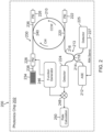
- FIG. 2 is a schematic illustration of an integrated photonics gyroscope 200 according to another embodiment.
- the photonics gyroscope 200 generally includes a waveguide resonator 210, such as a waveguide ring resonator, which is in optical communication with a broadband light source 212 through an optical path provided by a first waveguide arrangement 213.
- a waveguide resonator 210 such as a waveguide ring resonator
- Each of the components of photonics gyroscope 200 can be integrated on a single photonics chip 202.
- the waveguide resonator 210 can be formed to have a large polarization dependent loss, and to intrinsically support one polarization mode, which reduces bias error and instability in photonics gyroscope 200.
- the light source 212 can be an ASE device, such as at least one SLD, which is configured to emit a light beam with a broadband spectrum.
- the first waveguide arrangement 213 includes a first waveguide 214 optically coupled to an output of light source 212, and a second waveguide 216 optically coupled to waveguide resonator 210.
- a portion of first waveguide 214 is optically coupled to a portion of second waveguide 216 at a first coupler region 218.
- the second waveguide 216 is optically coupled to waveguide resonator 210 at a second coupler region 220 on a first side of waveguide resonator 210.
- the second waveguide 216 is optically coupled between first phase modulator 222 and an input of first optical detector 224.
- a second optical detector 225 on photonics chip 202 is operatively coupled to light source 202.
- the first waveguide 214 is optically coupled between light source 214 and second optical detector 225.
- An output from second optical detector 225 communicates with an input of light source 212 to form a RIN servo 227, which is configured to stabilize an intensity of the light beam emitted from light source 212.
- a second phase modulator 226 and a third phase modulator 228, on photonics chip 202 are in optical communication with waveguide resonator 210 through a second waveguide arrangement 230.
- a reflective component 234, such as a Bragg grating or an edge HR coating on a waveguide edge, is in optical communication with waveguide resonator 210 through second waveguide arrangement 230 and third phase modulator 228.
- the second waveguide arrangement 230 comprises a third waveguide 236 optically coupled between second phase modulator 226 and third phase modulator 228, and a fourth waveguide 238 optically coupled between reflective component 234 and third phase modulator 228.
- the third waveguide 236 is optically coupled to waveguide resonator 210 at a third coupler region 240 on a second side of waveguide resonator 210.
- first phase modulator 222 and second phase modulator 226 can each be terminated with a large angle cleave (e.g., greater than about 10 degrees), which reduces the back reflection light.
- the first phase modulator 222 and second phase modulator 226 are configured to reduce the bias instability due to the back reflection light by scrambling the phase of any reflected beam to cancel out the back reflection light, which can interfere and cause some bias.
- a low frequency modulation e.g., about 100 Hz
- a function generator 246 on photonics chip 202 is configured to send a control signal to third phase modulator 228 to impress two phase modulation waveforms at two different frequencies on the light.
- the first is at a modulation frequency f pm (e.g., about 20 kHz) and is used for rate detection, and the second is at a frequency f 3 (e.g., about 100 Hz) and is used to scramble the phase of the light propagated in optical paths including waveguide arrangement 230, phase modulator 228, and reflective component 234. This latter modulation suppresses the bias errors due to parasitic interference of light in those paths.
- a mixer 248 on photonics chip 292 is configured to receive a signal (modulation frequency (f pm )) from function generator 248 and an output signal from first optical detector 224.
- the mixer 248 combines the signals from function generator 246 and the first optical detector 224 to produce a combined signal.
- a rate calculation unit 250 on photonics chip 202 is configured to receive the combined signal form mixer 248.
- the rate calculation unit 250 is operative to calculate a rotation rate signal for photonics gyroscope 200.
- RIN servo 227, function generator 246, mixer 248, and rate calculation unit 250 are located on photonics chip 202. In other embodiments, one or more of these electronic components can be implemented off of photonics chip 202.
- a light beam is emitted from light source 212 into first waveguide 214, which directs the light beam to first coupler region 218 where a first portion of the light beam is coupled into second waveguide 216.
- a second portion of the light beam continues in first waveguide 214 and is directed to an input of second detector 225.
- the first portion of the light beam is directed by second waveguide 216 to second coupler region 220, which couples the light beam into waveguide resonator 210 in a CCW direction as a CCW beam.
- Any light not coupled into waveguide resonator 210 is directed by second waveguide 216 to first phase modulator 222, which scrambles the phase of this light to cancel out any back reflection of the light.
- a second portion of the light beam from light source 212 is directed to an input of second detector 225.
- a corresponding electrical signal is sent from second optical detector 225 to an input of light source 212 to provide a feedback loop for RIN servo 227, which stabilizes the intensity of the light beam emitted from light source 212.
- RIN servo 227 can have noise-reduction in a region around a modulation frequency f pm , potentially chosen to be anywhere in a frequency range from about 20 KHz to about 20 MHz.
- a beam portion of the CCW beam in waveguide resonator 210 is optically coupled into third waveguide 236 at third coupler region 240.
- the beam portion is phase modulated by third phase modulator 228 and directed to reflective component 234 through fourth waveguide 238.
- the reflective component 234 reflects the beam portion back through fourth waveguide 238, to third phase modulator 228, and into third waveguide 236.
- Some of the reflected beam portion is optically coupled at third coupler region 240 into waveguide resonator 210 in a CW direction as a CW beam.
- the remainder of the reflected beam portion in third waveguide 136 is directed to second phase modulator 226, which scrambles the phase of the reflected beam portion to cancel out any errors due to back reflected light.
- the CW beam is coupled out of waveguide resonator 210 at second coupler region 220 into second waveguide 216, and the CW beam is directed to first optical detector 224.
- the rotation of photonics gyroscope 200 causes a resonance frequency shift between the CW and CCW beams output by waveguide resonator 210, which is detected by first optical detector 224.
- the first optical detector 224 outputs a corresponding electrical signal that is demodulated at f m in mixer 248, which outputs a signal that is sent to rate calculation unit 250 for further processing to determine a rotation rate.
- the output intensity varies with the Sagnac frequency shift.
- the phase modulation and demodulation process convert the intensity output from a resonance peak to a linear output.
- the rotation rate magnitude and direction can be calculated from components of the demodulated signal, as well as using those components to suppress effects of the phase delay between phase modulator 228 and reflective component 234.
- Example 1 includes a photonics gyroscope, comprising: a light source on a photonics chip, the light source configured to emit a light beam with a broadband spectrum; a waveguide resonator on the photonics chip, the waveguide resonator in optical communication with the light source; a reflective component on the photonics chip and in optical communication with the waveguide resonator; a first optical detector on the photonics chip and in optical communication with the waveguide resonator; a second optical detector on the photonics chip and operatively coupled to the light source; a relative intensity noise (RIN) servo loop coupled between an output of the second optical detector and an input of the light source; and a rate calculation unit configured to receive a signal output from the first optical detector, the rate calculation unit operative to calculate a rotation rate signal for the photonics gyroscope; wherein the light beam from the light source is directed into the waveguide resonator such that the light beam propagates in a counterclockwise (CCW)
- Example 2 includes the photonics gyroscope of Example 1, wherein the light source comprises an amplified spontaneous emission device, a superluminescent diode, or two or more superluminescent diodes having different center wavelengths.
- the light source comprises an amplified spontaneous emission device, a superluminescent diode, or two or more superluminescent diodes having different center wavelengths.
- Example 3 includes the photonics gyroscope of any of Examples 1-2, wherein the waveguide resonator comprises a waveguide ring resonator.
- Example 4 includes the photonics gyroscope of any of Examples 1-3, wherein the reflective component comprises a Bragg grating, or an edge high reflective coating on a waveguide edge.
- Example 5 includes the photonics gyroscope of any of Examples 1-4, wherein the waveguide resonator is in optical communication with the light source through an optical path provided by a first waveguide arrangement.
- Example 6 includes the photonics gyroscope of Example 5, further comprising a first phase modulator on the photonics chip and in optical communication with the waveguide resonator through the first waveguide arrangement.
- Example 7 includes the photonics gyroscope of Example 6, wherein the first waveguide arrangement comprises: a first waveguide optically coupled to an output of the light source; a second waveguide optically coupled to the waveguide resonator; wherein a portion of the first waveguide is optically coupled to a portion of the second waveguide at a first coupler region; wherein the second waveguide is optically coupled to the waveguide resonator at a second coupler region on a first side of the waveguide resonator.
- Example 8 includes the photonics gyroscope of Example 7, wherein the second waveguide is optically coupled between the first phase modulator and an input of the first optical detector.
- Example 9 includes the photonics gyroscope of any of Examples 5-8, wherein the reflective component is in optical communication with the waveguide resonator through a second waveguide arrangement.
- Example 10 includes the photonics gyroscope of Example 9, further comprising: a second phase modulator on the photonics chip and in optical communication with the waveguide resonator through the second waveguide arrangement; and a third phase modulator on the photonics chip and in optical communication with the waveguide resonator through the second waveguide arrangement.
- Example 11 includes the photonics gyroscope of Example 10, further comprising: a function generator configured to send a control signal to the third phase modulator to adjust a phase modulation frequency; and a mixer configured to receive a signal from the function generator and an output signal from the first optical detector; wherein the mixer combines the signals from the function generator and the first optical detector to produce a combined signal that is sent to the rate calculation unit.
- Example 12 includes the photonics gyroscope of any of Examples 10-11, wherein the second waveguide arrangement comprises: a third waveguide optically coupled between the second phase modulator and the third phase modulator; and a fourth waveguide optically coupled between the reflective component and the third phase modulator.
- Example 13 includes the photonics gyroscope of any of Examples 10-12, wherein a low frequency modulation is applied to the phase modulators to scramble the phase of reflected beams at the phase modulators, thereby allowing the phase modulators to reduce the bias error due to parasitic interference.
- Example 14 includes the photonics gyroscope of any of Examples 12-13, wherein the third waveguide is optically coupled to the waveguide resonator at a third coupler region on a second side of the waveguide resonator.
- Example 15 includes the photonics gyroscope of any of Examples 12-14, wherein the third waveguide is optically coupled to a portion of a fifth waveguide at a fourth coupler region, the fifth waveguide optically coupled between the second optical detector and a third optical detector.
- Example 16 includes the photonics gyroscope of Example 15, wherein the third optical detector is configured to monitor power of the reflected beam.
- Example 17 includes the photonics gyroscope of any of Examples 7-16, wherein the first waveguide is optically coupled between the light source and the second optical detector.
- Example 18 includes a photonics gyroscope, comprising: a light source on a photonics chip, the light source configured to emit a light beam with a broadband spectrum; a waveguide ring resonator on the photonics chip, the waveguide ring resonator in optical communication with the light source through an optical path provided by a first waveguide arrangement; a first phase modulator on the photonics chip and in optical communication with the waveguide ring resonator through the first waveguide arrangement; a reflective component on the photonics chip and in optical communication with the waveguide ring resonator through a second waveguide arrangement; a second phase modulator on the photonics chip and in optical communication with the waveguide ring resonator through the second waveguide arrangement; a third phase modulator on the photonics chip and in optical communication with the waveguide ring resonator through the second waveguide arrangement; a first optical detector on the photonics chip and in optical communication with the waveguide ring resonator and the first phase modulator
- Example 19 includes the photonics gyroscope of Example 18, wherein the light source comprises an amplified spontaneous emission device, a superluminescent diode, or two or more superluminescent diodes having different center wavelengths.
- the light source comprises an amplified spontaneous emission device, a superluminescent diode, or two or more superluminescent diodes having different center wavelengths.
- Example 20 includes the photonics gyroscope of any of Examples 18-19, wherein the reflective component comprises a Bragg grating, or an edge high reflective coating on a waveguide edge.
Landscapes
- Physics & Mathematics (AREA)
- Engineering & Computer Science (AREA)
- Electromagnetism (AREA)
- Optics & Photonics (AREA)
- Power Engineering (AREA)
- General Physics & Mathematics (AREA)
- Radar, Positioning & Navigation (AREA)
- Remote Sensing (AREA)
- Plasma & Fusion (AREA)
- Gyroscopes (AREA)
Abstract
Description
- The resonant optical gyroscope often requires narrow linewidth lasers for rate interrogation. One or multiple narrow linewidth lasers can be used to lock to the cavity resonances in the gyroscope. The rotation rate is determined by comparing the resonance shift between clockwise (CW) and counter-clockwise (CCW) beam directions. This narrow linewidth gyroscope system is expensive and complicated. In addition, the system bias performance is limited by the Kerr effect. The Kerr effect is caused by the different phase shifts between counter propagating beams due to the self-phase modulation (SPM) and cross-phase modulation (XPM) and is more prominent with narrow linewidth lasers.
- The Kerr bias becomes more significant in integrated photonics gyroscopes. Due to the small scale factor, or sensitivity rotation rate, photonics gyroscopes must have very high finesses to reduce the cavity linewidth and increase the gyroscope sensitivity. Therefore, the intracavity intensity of photonics gyroscopes is much higher than the intensity in traditional resonant fiber optical gyroscopes, leading to stronger Kerr effect.
- A photonics gyroscope comprises a light source on a photonics chip, the light source configured to emit a light beam with a broadband spectrum; a waveguide resonator on the photonics chip, the waveguide resonator in optical communication with the light source; a reflective component on the photonics chip and in optical communication with the waveguide resonator; a first optical detector on the photonics chip and in optical communication with the waveguide resonator; a second optical detector on the photonics chip and operatively coupled to the light source; a relative intensity noise (RIN) servo loop coupled between an output of the second optical detector and an input of the light source; and a rate calculation unit configured to receive a signal output from the first optical detector, the rate calculation unit operative to calculate a rotation rate signal for the photonics gyroscope. The light beam from the light source is directed into the waveguide resonator such that the light beam propagates in a counterclockwise (CCW) direction as a CCW beam in the waveguide resonator. A beam portion of the CCW beam is coupled out of the waveguide resonator toward the reflective component and reflected back by the reflective component as a reflected beam that is optically coupled into the waveguide resonator such that the reflected beam propagates in a clockwise (CW) direction as a CW beam in the waveguide resonator. The CW beam is coupled out of the waveguide resonator and directed to the first optical detector, which is operative to detect a resonance frequency shift between the CW and CCW beams caused by rotation of the photonics gyroscope. The RIN servo loop is configured to stabilize an intensity of the light beam emitted from the light source such that a bias error and noise in the photonics gyroscope is reduced.
- Features of the present invention will become apparent to those skilled in the art from the following description with reference to the drawings. Understanding that the drawings depict only typical embodiments and are not therefore to be considered limiting in scope, the invention will be described with additional specificity and detail through the use of the accompanying drawings, in which:
-
Figure 1 is a schematic illustration of a photonics gyroscope, according to one embodiment; and -
Figure 2 is a schematic illustration of a photonics gyroscope, according to another embodiment. - In the following detailed description, embodiments are described in sufficient detail to enable those skilled in the art to practice the invention. It is to be understood that other embodiments may be utilized without departing from the scope of the invention. The following detailed description is, therefore, not to be taken in a limiting sense.
- Photonics gyroscopes that utilize a broadband light source are described herein. A photonics gyroscope with a broadband light source compares the intensity difference between clockwise (CW) and counterclockwise (CCW) beam transmissions. The optical power at each resonant peak is low; therefore, a typical gyroscope measurement based on one single resonance peak is limited by the shot noise. However, using the broadband light source covers a significant amount (N) of resonance peaks. The Angle Random Walk (ARW) will be reduced from the shot noise limited ARW by a factor of the square root of N. The bias due to the Kerr effect is greatly reduced due to the broadband light source.
- The photonics gyroscope with a broadband light source is based on an optical waveguide resonator, such as a waveguide ring resonator, and waveguide coupler arrangements. An on-chip broadband light source, such as at least one superluminescent diode (SLD), emits a light beam that is split into two outputs via a coupler. In some embodiments, a couple of SLDs can be combined together for broader bandwidth and higher power. The light beam in one output is used for a relative intensity noise (RIN) servo loop to stabilize the light source intensity, such that a bias error and noise in the photonics gyroscope is reduced.
- The light beam from the other output is launched into the waveguide resonator in a CCW direction. This CCW light beam represents the transmission spectrum of the waveguide resonator in the CCW direction. The CCW light beam is then phase modulated and reflected by a reflective component, such as a Bragg grating fabricated on a waveguide, such that the reflected beam is directed in the CW direction in the waveguide resonator.
- The rotation of the photonics gyroscope causes the resonance frequency shift between CW and CCW directions. Thus, the output intensity varies with the Sagnac frequency shift. The phase modulation and demodulation process converts the intensity output from a resonance peak to a linear output. The rotation rate magnitude and direction can be calculated from components of the demodulated signal, as well as using those components to suppress effects of the phase delay error between a phase modulator and the reflective component. The linewidth of waveguide resonator can be designed to be wider than the maximum Sagnac frequency shift.
- Prior approaches for resonant optical gyroscopes rely on narrow linewidth lasers and resonance locking loops for rate detection, which is complicated and expensive. The present approach reduces the complexity and cost by using the broadband light source and integrates all the optical gyroscope components on a single photonics chip. Using a broadband light source significantly reduces the bias instability due to the Kerr effect.
- In addition, the present integrated photonics gyroscopes can significantly reduce size, weight, and power (SWaP) when implemented as a navigation-grade gyroscope. Also, complementary metal-oxide-semiconductor (CMOS) compatible integrated circuit manufacturing can be used to fabricate the photonics gyroscopes, providing significant cost reductions.
- Further details regarding the present approach are described as follows and with reference to the drawings.
-
Figure 1 is a schematic illustration of an integratedphotonics gyroscope 100 according to one embodiment. Thephotonics gyroscope 100 generally includes awaveguide resonator 110, such as a waveguide ring resonator, which is in optical communication with abroadband light source 112 through an optical path provided by afirst waveguide arrangement 113. As shown inFigure 1 , the optical components ofphotonics gyroscope 100 can be integrated on asingle photonics chip 102. - The
waveguide resonator 110 can be formed to have a large polarization dependent loss, and to intrinsically support one polarization mode, which reduces bias error and instability inphotonics gyroscope 100. In one embodiment,waveguide resonator 110 can have a cavity linewidth of about 1 MHz. Thelight source 112 can be an amplified spontaneous emission (ASE) device, such as a superluminescent diode (SLD), which is configured to emit a light beam with a broadband spectrum. In some embodiments, two or more SLDs with different center wavelengths can be combined to increase the power and bandwidth of the ASE light. - The
first waveguide arrangement 113 includes afirst waveguide 114 optically coupled to an output oflight source 112, and asecond waveguide 116 optically coupled towaveguide resonator 110. A portion offirst waveguide 114 is optically coupled to a portion ofsecond waveguide 116 at afirst coupler region 118. Thesecond waveguide 116 is optically coupled towaveguide resonator 110 at asecond coupler region 120 on a first side ofwaveguide resonator 110. - A first phase modulator (PM) 122 and a first
optical detector 124, onphotonics chip 102, are in optical communication withwaveguide resonator 110 throughfirst waveguide arrangement 113. Thesecond waveguide 116 is optically coupled betweenfirst phase modulator 122 and an input of firstoptical detector 124. Asecond phase modulator 130 and athird phase modulator 132, onphotonics chip 102, are in optical communication withwaveguide resonator 110 through asecond waveguide arrangement 133. - A
reflective component 134, such as a Bragg grating or an edge high reflective (HR) coating on a waveguide edge, is in optical communication withwaveguide resonator 110 throughsecond waveguide arrangement 133 andthird phase modulator 132. Thesecond waveguide arrangement 133 comprises athird waveguide 135 optically coupled betweensecond phase modulator 130 andthird phase modulator 132, and afourth waveguide 136 optically coupled betweenreflective component 134 andthird phase modulator 132. Thethird waveguide 135 is optically coupled towaveguide resonator 110 at athird coupler region 140 on a second side ofwaveguide resonator 110. Thethird waveguide 135 is also optically coupled to a portion of afifth waveguide 138 at afourth coupler region 142. Thefifth waveguide 138 is optically coupled between a secondoptical detector 143 and a thirdoptical detector 144. - An output from second
optical detector 143 communicates with an input oflight source 112 to form a relative intensity noise (RIN)servo 145, which is configured to stabilize the intensity of the light beam emitted fromlight source 112. The thirdoptical detector 144 is configured to monitor a reflected beam power. - The output of
first phase modulator 122 andsecond phase modulator 130 can each be terminated with a large angle cleave (e.g., greater than about 10 degrees), which reduces the back reflection light. Thefirst phase modulator 122 andsecond phase modulator 130 are configured to reduce the bias instability due to the back reflection light by scrambling the phase of any reflected beam to cancel out the back reflection light, which can interfere and cause bias instability in the gyroscope. In some embodiments, low frequency modulation (e.g., 100 Hz) can be used in all phase modulators to scramble the phase of the reflected beams at the phase modulators. In this way, the phase modulators are used to reduce the bias error due to parasitic light interference. - A
function generator 146 is configured to output a control signal tothird phase modulator 132 to impress two phase modulation waveforms at two different frequencies on the light. The first is at a modulation frequency fpm (e.g., about 20 kHz) and is used for rate detection, and the second is at a frequency f3 (e.g., about 100 Hz) and is used to scramble the phase of the light propagated in optical paths betweencoupler region 140 andreflective component 134. This latter modulation suppresses the bias errors due to parasitic interference of light in those paths. Amixer 148 is configured to receive a signal (modulation frequency (fpm)) fromfunction generator 146 and an output signal from firstoptical detector 124. Themixer 148 combines the signals fromfunction generator 146 and firstoptical detector 124 to produce a combined signal that is sent to arate calculation unit 150. - As shown in
Figure 1 ,RIN servo 145,function generator 146,mixer 148, andrate calculation unit 150 are implemented off ofphotonics chip 102. In other embodiments, one or more of these electronic components can be integrated onphotonics chip 102 using standard microfabrication processes. - During operation of
photonics gyroscope 100, a light beam is emitted frombroadband light source 112 intofirst waveguide 114, which directs the light beam tofirst coupler region 118 where the light beam is coupled intosecond waveguide 116. Thebroadband light source 112 contains (although not shown) an isolator to prevent lasing and other deleterious effects from potential optical feedback. The light beam is directed bysecond waveguide 116 tosecond coupler region 120, which couples the light beam intowaveguide resonator 110 in a CCW direction as a CCW beam. Any light not coupled intowaveguide resonator 110 is directed bysecond waveguide 116 tofirst phase modulator 122, which scrambles the phase of this light to cancel out any back reflection of the light. - A beam portion of the CCW beam in
waveguide resonator 110 is optically coupled intothird waveguide 135 atthird coupler region 140. The transmitted beam portion is phase modulated bythird phase modulator 132 and directed toreflective component 134 throughfourth waveguide 136. Thereflective component 134 reflects the beam portion back throughfourth waveguide 136, tothird phase modulator 132, and intothird waveguide 135. Some of the reflected beam portion is optically coupled atthird coupler region 140 intowaveguide resonator 110 in a CW direction as a CW beam. The remainder of the reflected beam portion inthird waveguide 135 is directed tosecond phase modulator 130, which scrambles the phase of the reflected beam portion to cancel out any errors due to back reflected light. - In addition, some of the CCW light in
third waveguide 135 is tapped intofifth waveguide 138 atfourth coupler region 142 and directed to secondoptical detector 143. Also, some of the reflected light inthird waveguide 135 is tapped intofifth waveguide 138 atfourth coupler region 142 and directed to thirdoptical detector 144. A corresponding electrical signal is sent from secondoptical detector 143 to an input oflight source 112 to provide a feedback loop forRIN servo 145, which stabilizes an intensity of the light beam emitted fromlight source 112. In one embodiment,RIN servo 145 can stabilize the ASE intensity in a range from about 20 KHz to about 20 MHz. The thirdoptical detector 144 uses the reflected light infifth waveguide 138 to monitor the reflected beam power, which is the intensity of the CW beam coupled intowaveguide resonator 110 and can be used for scale factor calibration or compensation. - The CW beam is coupled out of
waveguide resonator 110 atsecond coupler region 120 intosecond waveguide 116, and the CW beam is directed to firstoptical detector 124. The rotation ofphotonics gyroscope 100 causes a resonance frequency shift between the CW and CCW beams output bywaveguide resonator 110, which is detected by firstoptical detector 124. The firstoptical detector 124 outputs a corresponding electrical signal that is demodulated at fm inmixer 148, which outputs a signal that is sent torate calculation unit 150 for further processing to determine a rotation rate. - The output intensity varies with the Sagnac frequency shift. The phase modulation and demodulation process convert the intensity output from a resonance peak to a linear output. The rotation rate magnitude and direction can be calculated from components of the demodulated signal, as well as using those components to suppress effects of the phase delay variations between
phase modulator 132 andreflective component 134. -
Figure 2 is a schematic illustration of anintegrated photonics gyroscope 200 according to another embodiment. Thephotonics gyroscope 200 generally includes awaveguide resonator 210, such as a waveguide ring resonator, which is in optical communication with abroadband light source 212 through an optical path provided by afirst waveguide arrangement 213. Each of the components ofphotonics gyroscope 200 can be integrated on asingle photonics chip 202. - The
waveguide resonator 210 can be formed to have a large polarization dependent loss, and to intrinsically support one polarization mode, which reduces bias error and instability inphotonics gyroscope 200. Thelight source 212 can be an ASE device, such as at least one SLD, which is configured to emit a light beam with a broadband spectrum. - The
first waveguide arrangement 213 includes afirst waveguide 214 optically coupled to an output oflight source 212, and asecond waveguide 216 optically coupled towaveguide resonator 210. A portion offirst waveguide 214 is optically coupled to a portion ofsecond waveguide 216 at afirst coupler region 218. Thesecond waveguide 216 is optically coupled towaveguide resonator 210 at asecond coupler region 220 on a first side ofwaveguide resonator 210. - A first phase modulator (PM) 222 and a first
optical detector 224, onphotonics chip 202, are in optical communication withwaveguide resonator 210 throughfirst waveguide arrangement 213. Thesecond waveguide 216 is optically coupled betweenfirst phase modulator 222 and an input of firstoptical detector 224. - A second
optical detector 225 onphotonics chip 202 is operatively coupled tolight source 202. Thefirst waveguide 214 is optically coupled betweenlight source 214 and secondoptical detector 225. An output from secondoptical detector 225 communicates with an input oflight source 212 to form aRIN servo 227, which is configured to stabilize an intensity of the light beam emitted fromlight source 212. - A
second phase modulator 226 and athird phase modulator 228, onphotonics chip 202, are in optical communication withwaveguide resonator 210 through asecond waveguide arrangement 230. Areflective component 234, such as a Bragg grating or an edge HR coating on a waveguide edge, is in optical communication withwaveguide resonator 210 throughsecond waveguide arrangement 230 andthird phase modulator 228. Thesecond waveguide arrangement 230 comprises athird waveguide 236 optically coupled betweensecond phase modulator 226 andthird phase modulator 228, and afourth waveguide 238 optically coupled betweenreflective component 234 andthird phase modulator 228. Thethird waveguide 236 is optically coupled towaveguide resonator 210 at athird coupler region 240 on a second side ofwaveguide resonator 210. - The output of
first phase modulator 222 andsecond phase modulator 226 can each be terminated with a large angle cleave (e.g., greater than about 10 degrees), which reduces the back reflection light. Thefirst phase modulator 222 andsecond phase modulator 226 are configured to reduce the bias instability due to the back reflection light by scrambling the phase of any reflected beam to cancel out the back reflection light, which can interfere and cause some bias. In some embodiments, a low frequency modulation (e.g., about 100 Hz) can be used in all the phase modulators to scramble the phase of the reflected beams at the phase modulators. The allows the phase modulators to reduce the bias error due to parasitic interference. - A
function generator 246 onphotonics chip 202 is configured to send a control signal tothird phase modulator 228 to impress two phase modulation waveforms at two different frequencies on the light. The first is at a modulation frequency fpm (e.g., about 20 kHz) and is used for rate detection, and the second is at a frequency f3 (e.g., about 100 Hz) and is used to scramble the phase of the light propagated in optical paths includingwaveguide arrangement 230,phase modulator 228, andreflective component 234. This latter modulation suppresses the bias errors due to parasitic interference of light in those paths. Amixer 248 on photonics chip 292 is configured to receive a signal (modulation frequency (fpm)) fromfunction generator 248 and an output signal from firstoptical detector 224. Themixer 248 combines the signals fromfunction generator 246 and the firstoptical detector 224 to produce a combined signal. Arate calculation unit 250 onphotonics chip 202 is configured to receive the combinedsignal form mixer 248. Therate calculation unit 250 is operative to calculate a rotation rate signal forphotonics gyroscope 200. - As shown in
Figure 2 ,RIN servo 227,function generator 246,mixer 248, andrate calculation unit 250 are located onphotonics chip 202. In other embodiments, one or more of these electronic components can be implemented off ofphotonics chip 202. - During operation of
photonics gyroscope 200, a light beam is emitted fromlight source 212 intofirst waveguide 214, which directs the light beam tofirst coupler region 218 where a first portion of the light beam is coupled intosecond waveguide 216. A second portion of the light beam continues infirst waveguide 214 and is directed to an input ofsecond detector 225. The first portion of the light beam is directed bysecond waveguide 216 tosecond coupler region 220, which couples the light beam intowaveguide resonator 210 in a CCW direction as a CCW beam. Any light not coupled intowaveguide resonator 210 is directed bysecond waveguide 216 tofirst phase modulator 222, which scrambles the phase of this light to cancel out any back reflection of the light. - As mentioned above, a second portion of the light beam from
light source 212 is directed to an input ofsecond detector 225. A corresponding electrical signal is sent from secondoptical detector 225 to an input oflight source 212 to provide a feedback loop forRIN servo 227, which stabilizes the intensity of the light beam emitted fromlight source 212. In one embodiment,RIN servo 227 can have noise-reduction in a region around a modulation frequency fpm, potentially chosen to be anywhere in a frequency range from about 20 KHz to about 20 MHz. - A beam portion of the CCW beam in
waveguide resonator 210 is optically coupled intothird waveguide 236 atthird coupler region 240. The beam portion is phase modulated bythird phase modulator 228 and directed toreflective component 234 throughfourth waveguide 238. Thereflective component 234 reflects the beam portion back throughfourth waveguide 238, tothird phase modulator 228, and intothird waveguide 236. Some of the reflected beam portion is optically coupled atthird coupler region 240 intowaveguide resonator 210 in a CW direction as a CW beam. The remainder of the reflected beam portion inthird waveguide 136 is directed tosecond phase modulator 226, which scrambles the phase of the reflected beam portion to cancel out any errors due to back reflected light. - The CW beam is coupled out of
waveguide resonator 210 atsecond coupler region 220 intosecond waveguide 216, and the CW beam is directed to firstoptical detector 224. The rotation ofphotonics gyroscope 200 causes a resonance frequency shift between the CW and CCW beams output bywaveguide resonator 210, which is detected by firstoptical detector 224. The firstoptical detector 224 outputs a corresponding electrical signal that is demodulated at fm inmixer 248, which outputs a signal that is sent torate calculation unit 250 for further processing to determine a rotation rate. - The output intensity varies with the Sagnac frequency shift. The phase modulation and demodulation process convert the intensity output from a resonance peak to a linear output. The rotation rate magnitude and direction can be calculated from components of the demodulated signal, as well as using those components to suppress effects of the phase delay between
phase modulator 228 andreflective component 234. - Example 1 includes a photonics gyroscope, comprising: a light source on a photonics chip, the light source configured to emit a light beam with a broadband spectrum; a waveguide resonator on the photonics chip, the waveguide resonator in optical communication with the light source; a reflective component on the photonics chip and in optical communication with the waveguide resonator; a first optical detector on the photonics chip and in optical communication with the waveguide resonator; a second optical detector on the photonics chip and operatively coupled to the light source; a relative intensity noise (RIN) servo loop coupled between an output of the second optical detector and an input of the light source; and a rate calculation unit configured to receive a signal output from the first optical detector, the rate calculation unit operative to calculate a rotation rate signal for the photonics gyroscope; wherein the light beam from the light source is directed into the waveguide resonator such that the light beam propagates in a counterclockwise (CCW) direction as a CCW beam in the waveguide resonator; wherein a beam portion of the CCW beam is coupled out of the waveguide resonator toward the reflective component and reflected back by the reflective component as a reflected beam that is optically coupled into the waveguide resonator such that the reflected beam propagates in a clockwise (CW) direction as a CW beam in the waveguide resonator; wherein the CW beam is coupled out of the waveguide resonator and directed to the first optical detector, which is operative to detect a resonance frequency shift between the CW and CCW beams caused by rotation of the photonics gyroscope; wherein the RIN servo loop is configured to stabilize an intensity of the light beam emitted from the light source such that a bias error and noise in the photonics gyroscope is reduced.
- Example 2 includes the photonics gyroscope of Example 1, wherein the light source comprises an amplified spontaneous emission device, a superluminescent diode, or two or more superluminescent diodes having different center wavelengths.
- Example 3 includes the photonics gyroscope of any of Examples 1-2, wherein the waveguide resonator comprises a waveguide ring resonator.
- Example 4 includes the photonics gyroscope of any of Examples 1-3, wherein the reflective component comprises a Bragg grating, or an edge high reflective coating on a waveguide edge.
- Example 5 includes the photonics gyroscope of any of Examples 1-4, wherein the waveguide resonator is in optical communication with the light source through an optical path provided by a first waveguide arrangement.
- Example 6 includes the photonics gyroscope of Example 5, further comprising a first phase modulator on the photonics chip and in optical communication with the waveguide resonator through the first waveguide arrangement.
- Example 7 includes the photonics gyroscope of Example 6, wherein the first waveguide arrangement comprises: a first waveguide optically coupled to an output of the light source; a second waveguide optically coupled to the waveguide resonator; wherein a portion of the first waveguide is optically coupled to a portion of the second waveguide at a first coupler region; wherein the second waveguide is optically coupled to the waveguide resonator at a second coupler region on a first side of the waveguide resonator.
- Example 8 includes the photonics gyroscope of Example 7, wherein the second waveguide is optically coupled between the first phase modulator and an input of the first optical detector.
- Example 9 includes the photonics gyroscope of any of Examples 5-8, wherein the reflective component is in optical communication with the waveguide resonator through a second waveguide arrangement.
- Example 10 includes the photonics gyroscope of Example 9, further comprising: a second phase modulator on the photonics chip and in optical communication with the waveguide resonator through the second waveguide arrangement; and a third phase modulator on the photonics chip and in optical communication with the waveguide resonator through the second waveguide arrangement.
- Example 11 includes the photonics gyroscope of Example 10, further comprising: a function generator configured to send a control signal to the third phase modulator to adjust a phase modulation frequency; and a mixer configured to receive a signal from the function generator and an output signal from the first optical detector; wherein the mixer combines the signals from the function generator and the first optical detector to produce a combined signal that is sent to the rate calculation unit.
- Example 12 includes the photonics gyroscope of any of Examples 10-11, wherein the second waveguide arrangement comprises: a third waveguide optically coupled between the second phase modulator and the third phase modulator; and a fourth waveguide optically coupled between the reflective component and the third phase modulator.
- Example 13 includes the photonics gyroscope of any of Examples 10-12, wherein a low frequency modulation is applied to the phase modulators to scramble the phase of reflected beams at the phase modulators, thereby allowing the phase modulators to reduce the bias error due to parasitic interference.
- Example 14 includes the photonics gyroscope of any of Examples 12-13, wherein the third waveguide is optically coupled to the waveguide resonator at a third coupler region on a second side of the waveguide resonator.
- Example 15 includes the photonics gyroscope of any of Examples 12-14, wherein the third waveguide is optically coupled to a portion of a fifth waveguide at a fourth coupler region, the fifth waveguide optically coupled between the second optical detector and a third optical detector.
- Example 16 includes the photonics gyroscope of Example 15, wherein the third optical detector is configured to monitor power of the reflected beam.
- Example 17 includes the photonics gyroscope of any of Examples 7-16, wherein the first waveguide is optically coupled between the light source and the second optical detector.
- Example 18 includes a photonics gyroscope, comprising: a light source on a photonics chip, the light source configured to emit a light beam with a broadband spectrum; a waveguide ring resonator on the photonics chip, the waveguide ring resonator in optical communication with the light source through an optical path provided by a first waveguide arrangement; a first phase modulator on the photonics chip and in optical communication with the waveguide ring resonator through the first waveguide arrangement; a reflective component on the photonics chip and in optical communication with the waveguide ring resonator through a second waveguide arrangement; a second phase modulator on the photonics chip and in optical communication with the waveguide ring resonator through the second waveguide arrangement; a third phase modulator on the photonics chip and in optical communication with the waveguide ring resonator through the second waveguide arrangement; a first optical detector on the photonics chip and in optical communication with the waveguide ring resonator and the first phase modulator through the first waveguide arrangement; a second optical detector on the photonics chip and operatively coupled to the light source; a relative intensity noise (RIN) servo loop coupled between an output of the second optical detector and an input of the light source; a function generator configured to send a control signal to the third phase modulator to adjust a phase modulation frequency; a mixer configured to receive a signal from the function generator and an output signal from the first optical detector, wherein the mixer is configured to combine the received signals to produce a combined signal; a rate calculation unit on the photonics chip and configured to receive the combined signal from the mixer, the rate calculation unit operative to calculate a rotation rate signal for the photonics gyroscope; wherein the light beam from the light source is directed into the waveguide ring resonator by the first waveguide arrangement such that the light beam propagates in a counterclockwise (CCW) direction as a CCW beam in the waveguide ring resonator; wherein a beam portion of the CCW beam is coupled out of the waveguide resonator into the second waveguide arrangement and toward the reflective component, which reflects the beam portion back along the second waveguide arrangement as a reflected beam that is optically coupled into the waveguide ring resonator, such that the reflected beam propagates in a clockwise (CW) direction as a CW beam in the waveguide ring resonator; wherein the CW beam is coupled out of the waveguide ring resonator into the first waveguide arrangement and directed to the first optical detector, which is operative to detect a resonance frequency shift between the CW and CCW beams caused by rotation of the photonics gyroscope; wherein the RIN servo loop is configured to stabilize an intensity of the light beam emitted from the light source such that a bias error and noise in the photonics gyroscope is reduced.
- Example 19 includes the photonics gyroscope of Example 18, wherein the light source comprises an amplified spontaneous emission device, a superluminescent diode, or two or more superluminescent diodes having different center wavelengths.
- Example 20 includes the photonics gyroscope of any of Examples 18-19, wherein the reflective component comprises a Bragg grating, or an edge high reflective coating on a waveguide edge.
- From the foregoing, it will be appreciated that, although specific embodiments have been described herein for purposes of illustration, various modifications may be made without deviating from the scope of the disclosure. Thus, the described embodiments are to be considered in all respects only as illustrative and not restrictive. In addition, all changes that come within the meaning and range of equivalency of the claims are to be embraced within their scope.
Claims (10)
- A photonics gyroscope, comprising:a light source on a photonics chip, the light source configured to emit a light beam with a broadband spectrum;a waveguide resonator on the photonics chip, the waveguide resonator in optical communication with the light source;a reflective component on the photonics chip and in optical communication with the waveguide resonator;a first optical detector on the photonics chip and in optical communication with the waveguide resonator;a second optical detector on the photonics chip and operatively coupled to the light source;a relative intensity noise (RIN) servo loop coupled between an output of the second optical detector and an input of the light source; anda rate calculation unit configured to receive a signal output from the first optical detector, the rate calculation unit operative to calculate a rotation rate signal for the photonics gyroscope;wherein the light beam from the light source is directed into the waveguide resonator such that the light beam propagates in a counterclockwise (CCW) direction as a CCW beam in the waveguide resonator;wherein a beam portion of the CCW beam is coupled out of the waveguide resonator toward the reflective component and reflected back by the reflective component as a reflected beam that is optically coupled into the waveguide resonator such that the reflected beam propagates in a clockwise (CW) direction as a CW beam in the waveguide resonator;wherein the CW beam is coupled out of the waveguide resonator and directed to the first optical detector, which is operative to detect a resonance frequency shift between the CW and CCW beams caused by rotation of the photonics gyroscope;wherein the RIN servo loop is configured to stabilize an intensity of the light beam emitted from the light source such that a bias error and noise in the photonics gyroscope is reduced.
- The photonics gyroscope of claim 1, wherein the light source comprises an amplified spontaneous emission device, a superluminescent diode, or two or more superluminescent diodes having different center wavelengths.
- The photonics gyroscope of claim 1, wherein the waveguide resonator is in optical communication with the light source through an optical path provided by a first waveguide arrangement.
- The photonics gyroscope of claim 3, further comprising a first phase modulator on the photonics chip and in optical communication with the waveguide resonator through the first waveguide arrangement.
- The photonics gyroscope of claim 4, wherein the first waveguide arrangement comprises:a first waveguide optically coupled to an output of the light source;a second waveguide optically coupled to the waveguide resonator;wherein a portion of the first waveguide is optically coupled to a portion of the second waveguide at a first coupler region;wherein the second waveguide is optically coupled to the waveguide resonator at a second coupler region on a first side of the waveguide resonator.
- The photonics gyroscope of claim 5, wherein:the second waveguide is optically coupled between the first phase modulator and an input of the first optical detector; andthe reflective component is in optical communication with the waveguide resonator through a second waveguide arrangement.
- The photonics gyroscope of claim 6, further comprising:a second phase modulator on the photonics chip and in optical communication with the waveguide resonator through the second waveguide arrangement; anda third phase modulator on the photonics chip and in optical communication with the waveguide resonator through the second waveguide arrangement.
- The photonics gyroscope of claim 7, further comprising:a function generator configured to send a control signal to the third phase modulator to adjust a phase modulation frequency; anda mixer configured to receive a signal from the function generator and an output signal from the first optical detector;wherein the mixer combines the signals from the function generator and the first optical detector to produce a combined signal that is sent to the rate calculation unit.
- The photonics gyroscope of claim 8, wherein the second waveguide arrangement comprises:a third waveguide optically coupled between the second phase modulator and the third phase modulator; anda fourth waveguide optically coupled between the reflective component and the third phase modulator;wherein the third waveguide is optically coupled to the waveguide resonator at a third coupler region on a second side of the waveguide resonator.
- The photonics gyroscope of claim 9, wherein the third waveguide is optically coupled to a portion of a fifth waveguide at a fourth coupler region, the fifth waveguide optically coupled between the second optical detector and a third optical detector;
wherein the third optical detector is configured to monitor power of the reflected beam.
Applications Claiming Priority (1)
| Application Number | Priority Date | Filing Date | Title |
|---|---|---|---|
| US18/193,448 US12345530B2 (en) | 2023-03-30 | 2023-03-30 | Photonics gyroscope with broadband light source |
Publications (1)
| Publication Number | Publication Date |
|---|---|
| EP4439011A1 true EP4439011A1 (en) | 2024-10-02 |
Family
ID=90362130
Family Applications (1)
| Application Number | Title | Priority Date | Filing Date |
|---|---|---|---|
| EP24161512.9A Pending EP4439011A1 (en) | 2023-03-30 | 2024-03-05 | Photonics gyroscope with broadband light source |
Country Status (2)
| Country | Link |
|---|---|
| US (1) | US12345530B2 (en) |
| EP (1) | EP4439011A1 (en) |
Families Citing this family (2)
| Publication number | Priority date | Publication date | Assignee | Title |
|---|---|---|---|---|
| US12123718B1 (en) * | 2023-04-11 | 2024-10-22 | Anello Photonics, Inc. | Mitigating bias instabilities in optical gyroscopes |
| US12405111B2 (en) * | 2023-07-06 | 2025-09-02 | Honeywell International Inc. | Resonator optical gyroscopes with dual broadband light sources |
Citations (1)
| Publication number | Priority date | Publication date | Assignee | Title |
|---|---|---|---|---|
| US5327215A (en) * | 1991-10-24 | 1994-07-05 | Bodenseewerk Geratetechnik Gmbh | Sensor having optical passive ring resonator using sagnac effect |
Family Cites Families (17)
| Publication number | Priority date | Publication date | Assignee | Title |
|---|---|---|---|---|
| US20040061863A1 (en) | 2002-08-20 | 2004-04-01 | Digonnet Michel J.F. | Fiber optic sensors with reduced noise |
| US7738109B2 (en) | 2002-08-20 | 2010-06-15 | The Board Of Trustees Of The Leland Stanford Junior University | Fiber optic sensor using a Bragg fiber |
| US7619743B2 (en) | 2006-06-29 | 2009-11-17 | The Board Of Trustees Of The Leland Stanford Junior University | Optical sensor utilizing hollow-core photonic bandgap fiber with low phase thermal constant |
| US7911619B2 (en) | 2007-11-15 | 2011-03-22 | The Board Of Trustees Of The Leland Stanford Junior University | Low-noise fiber optic sensor utilizing a laser source |
| US8744222B2 (en) | 2011-07-27 | 2014-06-03 | National Applied Research Laboratories | Practical silicon photonic multi-function integrated-optic chip for fiber sensor applications |
| US9121708B1 (en) * | 2014-05-08 | 2015-09-01 | Honeywell International Inc. | Resonator fiber optic gyroscope without frequency overlap in sideband-heterodyne-detection modulations |
| US9733084B2 (en) * | 2015-09-09 | 2017-08-15 | Honeywell International Inc. | Single pump cascaded stimulated Brillouin scattering (SBS) ring laser gyro |
| EP3516333B1 (en) | 2016-09-20 | 2023-05-03 | The Board of Trustees of the Leland Stanford Junior University | Optical system and method utilizing a laser-driven light source with white noise modulation |
| KR102551725B1 (en) * | 2017-03-09 | 2023-07-06 | 케이브이에이치 인더스트리즈, 인코포레이티드 | Photon Integrated Circuits for Interferometric Fiber Optic Gyroscopes (IFOGs) |
| US11320267B2 (en) | 2017-03-23 | 2022-05-03 | Kvh Industries, Inc. | Integrated optic wavemeter and method for fiber optic gyroscopes scale factor stabilization |
| US10725243B2 (en) | 2017-04-27 | 2020-07-28 | The Charles Stark Draper Laboratory, Inc. | Stabilized broadband light source apparatus and methods |
| US10852137B2 (en) | 2017-09-29 | 2020-12-01 | Gener8, LLC | Multilayer waveguide optical gyroscope |
| US10731988B1 (en) | 2019-07-10 | 2020-08-04 | Anello Photonics, Inc. | System architecture for integrated photonics optical gyroscopes |
| US11506496B2 (en) | 2019-07-10 | 2022-11-22 | Anello Photonics, Inc. | System architecture for integrated photonics optical gyroscopes |
| IT202000005710A1 (en) | 2020-03-18 | 2021-09-18 | Civitanavi Systems Spa | Semi-finished product for the construction of a gyroscope and gyroscope including the semi-finished product. |
| US11231278B1 (en) | 2020-10-15 | 2022-01-25 | The Board Of Trustees Of The Leland Stanford Junior University | System and method for generating broadband spectrum by phase modulation of multiple wavelengths |
| CN116888748A (en) | 2020-12-16 | 2023-10-13 | 实光半导体私人有限公司 | Photonic integrated chip |
-
2023
- 2023-03-30 US US18/193,448 patent/US12345530B2/en active Active
-
2024
- 2024-03-05 EP EP24161512.9A patent/EP4439011A1/en active Pending
Patent Citations (1)
| Publication number | Priority date | Publication date | Assignee | Title |
|---|---|---|---|---|
| US5327215A (en) * | 1991-10-24 | 1994-07-05 | Bodenseewerk Geratetechnik Gmbh | Sensor having optical passive ring resonator using sagnac effect |
Also Published As
| Publication number | Publication date |
|---|---|
| US20240328783A1 (en) | 2024-10-03 |
| US12345530B2 (en) | 2025-07-01 |
Similar Documents
| Publication | Publication Date | Title |
|---|---|---|
| US9587945B2 (en) | Symmetric three-laser resonator fiber optic gyroscope | |
| US9537283B2 (en) | Laser with transmission and reflection mode feedback control | |
| US9115994B2 (en) | Systems and methods sideband heterodyning detection | |
| US12345530B2 (en) | Photonics gyroscope with broadband light source | |
| US10928200B1 (en) | Frequency pulling reduction in SBS laser | |
| Sanders et al. | Improvements to signal processing and component minaturization of compact resonator fiber optic gyroscopes | |
| JP2014032384A (en) | Narrow bandwidth reflectors for reducing stimulated brillouin scattering in optical cavity | |
| US11486706B2 (en) | Kerr effect reduction in SBS laser gyroscope | |
| US5517305A (en) | Brillouin ring laser gyro | |
| EP4462074B1 (en) | Resonant optical gyroscope with broadband light source and rin reduction techniques | |
| US9170108B1 (en) | Controlled modulation of light beam with highly stable suppression of carrier or sidebands | |
| EP4521063A1 (en) | Optical gyroscope with broadband comb interrogation | |
| US12392612B2 (en) | Systems and methods for effective relative intensity noise subtraction for a broadband resonator optical gyroscope | |
| US12405111B2 (en) | Resonator optical gyroscopes with dual broadband light sources | |
| US6584246B1 (en) | Source, system and method for generating amplified stimulated emission using a coupler mechanism | |
| US12449258B2 (en) | Broadband resonator optical gyroscope with efficient optical power management for low shot noise | |
| EP4567380B1 (en) | Optical circuit for compensating optical lead fluctuations in an rfog | |
| US20250052575A1 (en) | Rfog employing serrodyne frequency shifting | |
| US20240302168A1 (en) | Integrated photonics gyroscope with common intensity modulation | |
| KR100527110B1 (en) | Millimeter wave generator based on the interferometer and optical detecting device |
Legal Events
| Date | Code | Title | Description |
|---|---|---|---|
| PUAI | Public reference made under article 153(3) epc to a published international application that has entered the european phase |
Free format text: ORIGINAL CODE: 0009012 |
|
| STAA | Information on the status of an ep patent application or granted ep patent |
Free format text: STATUS: THE APPLICATION HAS BEEN PUBLISHED |
|
| AK | Designated contracting states |
Kind code of ref document: A1 Designated state(s): AL AT BE BG CH CY CZ DE DK EE ES FI FR GB GR HR HU IE IS IT LI LT LU LV MC ME MK MT NL NO PL PT RO RS SE SI SK SM TR |
|
| STAA | Information on the status of an ep patent application or granted ep patent |
Free format text: STATUS: REQUEST FOR EXAMINATION WAS MADE |
|
| 17P | Request for examination filed |
Effective date: 20241118 |
|
| RBV | Designated contracting states (corrected) |
Designated state(s): AL AT BE BG CH CY CZ DE DK EE ES FI FR GB GR HR HU IE IS IT LI LT LU LV MC ME MK MT NL NO PL PT RO RS SE SI SK SM TR |