EP4436350A1 - Quantization breakdown protection for semiconductors and in particular topological insulators - Google Patents
Quantization breakdown protection for semiconductors and in particular topological insulators Download PDFInfo
- Publication number
- EP4436350A1 EP4436350A1 EP23162996.5A EP23162996A EP4436350A1 EP 4436350 A1 EP4436350 A1 EP 4436350A1 EP 23162996 A EP23162996 A EP 23162996A EP 4436350 A1 EP4436350 A1 EP 4436350A1
- Authority
- EP
- European Patent Office
- Prior art keywords
- edge
- electric contact
- electric
- segment
- electric potential
- Prior art date
- Legal status (The legal status is an assumption and is not a legal conclusion. Google has not performed a legal analysis and makes no representation as to the accuracy of the status listed.)
- Granted
Links
Images




Classifications
-
- H—ELECTRICITY
- H10—SEMICONDUCTOR DEVICES; ELECTRIC SOLID-STATE DEVICES NOT OTHERWISE PROVIDED FOR
- H10N—ELECTRIC SOLID-STATE DEVICES NOT OTHERWISE PROVIDED FOR
- H10N99/00—Subject matter not provided for in other groups of this subclass
- H10N99/05—Devices based on quantum mechanical effects, e.g. quantum interference devices or metal single-electron transistors
Definitions
- the present disclosure relates protecting structures made of semiconducting materials such as topological insulators from quantization breakdown.
- the present disclosure relates to protecting a structure made of a magnetic topological insulator against quantization breakdown which causes a bulk between a first edge of the structure and a second edge of the structure to conduct electrical charges between the edges.
- the charge transport within a magnetic topological insulator may be confined to its chiral edge states. See Fijalkowski, Kajetan M., Nan Liu, Pankaj Mandal, Steffen Schreyeck, Karl Brunner, Charles Gould, and Laurens W. Molenkamp. "Quantum Anomalous Hall Edge Channels Survive up to the Curie Temperature". Nature Communications 12, Nr. 1 (22. September 2021 ).
- chiral edge states may be created in a two-dimensional semiconductor in a magnetic field.
- the charge transport along a chiral edge may be quantized and used to determine the von Klitzing constant.
- the present invention is directed at a method of protecting a structure made of a semiconducting material against quantization breakdown which causes a bulk between a first edge of the structure and a second edge of the structure to conduct electrical charges between the edges. Furthermore, the present invention is directed at a measuring apparatus.
- a method according to the present invention comprises causing two independent electrical currents along the edges and adapting a first electric potential along a first segment of the first edge, which is delimited by a first electric contact and a second electric contact through which a first voltage is applied to the first segment, to a second electric potential along a second segment of the second edge, which is delimited by a third electric contact and a fourth electric contact through which a second voltage is applied to the second segment.
- the semiconducting material may be a magnetic topological insulator.
- magnetic topological insulator as used throughout the description and the claims, particularly refers to a material which exhibits quantum anomalous Hall conductivity along its edges.
- quantum anomalous Hall conductivity particularly refers to conditions under which the edges are electrically connected through the then-conducting bulk.
- bulk as used throughout the description and the claims, particularly refers to a material between the edges.
- the electric field caused by the second electric potential may compensate the electric field caused by the first electric potential such that the resulting electric field is significantly reduced, and in the ideal case becomes zero across the bulk. Otherwise, the uncompensated electric field caused by the first electric potential may result in electrical charge transport across the bulk.
- the structure may form a ring having an outer edge and an inner edge.
- the outer edge of the ring may constitute the first edge and the inner edge of the ring may constitute the second edge.
- the structure may be a multi-terminal Corbino device with two disconnected perimeters such as a Corbino ring with chiral inner and outer edges (i.e., dissipationless inner and outer chiral edge channels).
- the ring may be divided into a first half and a second half, wherein the first segment constitutes the outer edge of the first half and the second segment constitutes the inner edge of the first half. Accordingly, the first and second segments may lie at opposite sides of the bulk and (fully) overlap in the radial direction.
- the first electric contact and the third electric contact may be arranged at a first end of the first half, and the second electric contact and the fourth electric contact may be arranged at a second end of the first half.
- the second voltage between the third electric contact and the fourth electric contact may be inverse to the first voltage between the first electric contact and the second electric contact. Accordingly, the currents along the outer and inner edges may run in opposite directions.
- the electric potential of the first electric contact may be equal to an electric potential of the fourth electric contact, and an electric potential of the second electric contact may be equal to an electric potential of the third electric contact.
- first contact and the third contact may form a first contact pair
- second contact and the fourth contact may form a second contact pair
- the contacts forming a contact pair are (only) radially displaced relative to one another and the voltages across the contact pairs are inverse to each other.
- the above-described steps may be used in a method of determining the von Klitzing constant which comprises the further steps of measuring a third electric potential of the first edge between the first electric contact and the second electric contact, measuring a fourth electric potential of the first edge outside of the first segment, between the second electric contact and the first electric contact, and determining, based on the measured third electric potential and the measured fourth electric potential, the von Klitzing constant.
- the first and second edge can be assigned to be outer and inner edge or inner and outer edge.
- the structure may be exposed to an external magnetic field before or during measuring the third electric potential.
- the structure may be arranged in a measuring apparatus which further comprises a Josephson junction or a Josephson junction array.
- a measuring apparatus which further comprises a Josephson junction or a Josephson junction array.
- the structure and the Josephson junction (array) may form part of a Kibble balance.
- the structure and the Josephson junction or the Josephson junction array may be shielded from external magnetic fields while measuring the third and fourth electric potentials and collecting measurement data for determining the Josephson constant.
- a measuring apparatus comprises a structure made of a material hosting chiral edge states.
- the chiral edge states may result from cooling the material to below its Curie temperature in the case of a magnetic material, or alternatively by applying a magnetic field.
- the apparatus may also include a cooling device and a device to apply a magnetic field, as appropriate to generate the chiral edge states.
- the apparatus may also include a controller configured to inject a first electrical current into the first edge and a second electrical current into the second edge, wherein the controller is further configured to cause the first electrical current and the second electrical current to flow in opposite directions.
- the first electrical current may flow along a first path across a first segment of the first edge and the second electrical current may flow along a second path across a second segment of the second edge.
- the controller may be further configured to cause a voltage between the first segment and the second segment across a bulk of the structure to be zero.
- the inversely biased segments may compensate each other and thus avoid generating a non-zero electric field across the bulk.
- the structure may form a Corbino ring having an outer edge and an inner edge.
- the outer edge of the Corbino ring may constitute the first edge and the inner edge of the Corbino ring may constitute the second edge.
- the Corbino ring may comprise a first half and a second half.
- the first segment may constitute the outer edge of the first half and the second segment may constitute the inner edge of the first half.
- the measuring apparatus may further comprise a first electric contact and a third electric contact arranged at a first end of the first half, and a second electric contact and a fourth electric contact arranged at a second end of the first half, wherein a first voltage between the first electric contact and the second electric contact drives the first electrical current and a second voltage between the third electric contact and the fourth electric contact drives the second electrical current.
- An electric potential of the first electric contact may be equal to an electric potential of the fourth electric contact, and an electric potential of the second electric contact may be equal to an electric potential of the third electric contact.
- the (optional) features of the method may be (optional) features of the apparatus and vice versa.
- Fig. 1 shows a structure 10 made of a semiconducting material such as a magnetically doped topological insulator (e.g., V 0.1 (Bi 0.2 Sb 0.8 ) 1.9 Te 3 ) which has been cooled by a cooling device (not shown) to below its Curie temperature T C .
- a magnetically doped topological insulator e.g., V 0.1 (Bi 0.2 Sb 0.8 ) 1.9 Te 3
- T C Curie temperature
- a two-dimensional semiconductor operating in a magnetic field may also be used to produce the chiral edge states.
- the structure 10 may be arranged in an apparatus 34 which comprises a controller 36.
- the controller 36 may be configured to inject an electrical current I 1 through electric contact 18 into the outer chiral edge 12 by applying a voltage to outer electric contacts 18 and 22.
- the controller 36 may be configured to inject an electrical current I 2 through electric contact 30 into the inner chiral edge 14 by applying a voltage to inner electric contacts 26 and 30.
- the chiral edge segments 12a and 14a may then equilibrate the electric potential along the segments 12a and 14a with the (source) electric contacts 18 and 30, respectively.
- the electric contacts 22 and 26 may be grounded so that the chiral edge segments 12b and 14b may equilibrate the electric potential along those segments with ground.
- the first electrical current I 1 and the second electrical I 2 current may flow in opposite directions.
- the injected electrical currents I 1 and I 2 divide the chiral edges 12 and 14 into two segments 12a and 12b and 14a and 14b, respectively, which differ regarding the electric potential along the segments 12a and 12b and 14a and 14b, respectively. Because the segments 12a and 14a that exhibit the higher electric potential are arranged vis-à-vis each other (as are the segments 12b and 14b which exhibit the lower electric potential), the electric field across the bulk 16 may be significantly reduced, or ideally zero.
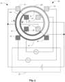
- the structure 10 may form a Corbino ring (instead of a rectangle as shown in Fig. 1 and Fig. 2 ) with the four electric contact pairs (i.e., electric contacts 18 and 26, 20 and 28, 22 and 30, and 24 and 32) being evenly distributed around the Corbino ring (at 0°, 90°, 180°, and 270°).
- injecting the electrical currents I 1 and I 2 may divide the ring into two halves (at 0° and 180°), delineated by electric contacts 18 and 26 on one end and electric contacts 22 and 30 on the other end (as indicated by the broken lines).
- the segments 12a and 14a which exhibit the higher electric potential fully overlap in the radial direction and cause the electric field across the bulk 16 to be substantially zero.
- the segments 12b and 14b which exhibit the lower electric potential e.g., ground.
- a plot representing the potential along the inner edge 14 and projected radially onto the outer edge 12 would match a plot representing the potential along the outer edge 12.
- using the structure 10 instead of a classical Hall bar allows for measurements at a much higher current as it avoids a (non-zero) electric field across the bulk 16 which would otherwise drive (or at least contribute to) the quantization breakdown.
- the controller 36 may measure the voltage between the segments 12a and 12b of the outer edge 12 (or alternatively, or in addition, the voltage between the segments 14a and 14b of the inner edge 14) to determine the von Klitzing constant based on the Quantum Anomalous Hall effect which is exhibited by magnetic topological isolators in the absence of a magnetic field (i.e., zero magnetic field). To this end, the controller 36 may be configured to measure the voltage(s) as a function of the injected electrical current(s).
- the structure 10 may also be used in conducting measurements which exploit the Quantum Hall effect.
- the first electrical current I 1 and the second electrical I 2 may be generated by two separate sources.
- the structure 10 may be provided with a gate contact 38 for tuning.
- the apparatus 34 may comprise a Josephson junction (not shown) to measure the Josephson constant (e.g., by exploiting the AC Josephson effect).
- a magnetic field generator may be switched off and/or the structure 10 and the Josephson junction or Josephson junction array may be shielded from external magnetic fields.
- the structure 10 and the Josephson junction or Josephson junction array may be integrated into a Kibble balance.
- a process for protecting the structure 10 against quantization breakdown may start with a step 40 of causing independent electrical currents I 1 and I 2 along the chiral edges 12 and 14. The process may then be continued at step 42 by adapting a first electric potential along a segment 12a of the edge 12, which is delimited by the electric contacts 18 and 22 through which a voltage is applied to the segment 12a, to a second electric potential along a segment 14a of the edge 14, which is delimited by electric contacts 26 and 30 through which the same voltage is applied to the segment 14a.
Landscapes
- Semiconductor Integrated Circuits (AREA)
Abstract
Description
- The present disclosure relates protecting structures made of semiconducting materials such as topological insulators from quantization breakdown. In particular, the present disclosure relates to protecting a structure made of a magnetic topological insulator against quantization breakdown which causes a bulk between a first edge of the structure and a second edge of the structure to conduct electrical charges between the edges.
- At low temperatures, the charge transport within a magnetic topological insulator may be confined to its chiral edge states. See Fijalkowski, Kajetan M., Nan Liu, Pankaj Mandal, Steffen Schreyeck, Karl Brunner, Charles Gould, and Laurens W. Molenkamp. "Quantum Anomalous Hall Edge Channels Survive up to the Curie Temperature". Nature Communications 12, Nr. 1 (22. September 2021). Alternatively, chiral edge states may be created in a two-dimensional semiconductor in a magnetic field. Moreover, the charge transport along a chiral edge may be quantized and used to determine the von Klitzing constant.
- The present invention is directed at a method of protecting a structure made of a semiconducting material against quantization breakdown which causes a bulk between a first edge of the structure and a second edge of the structure to conduct electrical charges between the edges. Furthermore, the present invention is directed at a measuring apparatus.
- A method according to the present invention comprises causing two independent electrical currents along the edges and adapting a first electric potential along a first segment of the first edge, which is delimited by a first electric contact and a second electric contact through which a first voltage is applied to the first segment, to a second electric potential along a second segment of the second edge, which is delimited by a third electric contact and a fourth electric contact through which a second voltage is applied to the second segment.
- The semiconducting material may be a magnetic topological insulator.
- In this regard, the term "magnetic topological insulator", as used throughout the description and the claims, particularly refers to a material which exhibits quantum anomalous Hall conductivity along its edges. Furthermore, the term "quantization breakdown", as used throughout the description and the claims, particularly refers to conditions under which the edges are electrically connected through the then-conducting bulk. Moreover, the term "bulk", as used throughout the description and the claims, particularly refers to a material between the edges.
- In addition, the formulation "segment delimited by electric contacts", as used throughout the description and the claims, particularly refers to a segment which extends from one contact to the other. Finally, the formulation "electric potential along a segment of the edge", as used throughout the description and the claims, particularly refers to a specific electric potential if the potential does not change along the segment or a function mapping different parts of the segment to different electric potentials if there are different electric potentials along the segment.
- Adapting the first electric potential to the second electric potential allows for ensuring a lower voltage across the bulk. This in turn protects the structure against breakdown for which the voltage is a driver. In other words, the electric field caused by the second electric potential may compensate the electric field caused by the first electric potential such that the resulting electric field is significantly reduced, and in the ideal case becomes zero across the bulk. Otherwise, the uncompensated electric field caused by the first electric potential may result in electrical charge transport across the bulk.
- The structure may form a ring having an outer edge and an inner edge. The outer edge of the ring may constitute the first edge and the inner edge of the ring may constitute the second edge. For example, the structure may be a multi-terminal Corbino device with two disconnected perimeters such as a Corbino ring with chiral inner and outer edges (i.e., dissipationless inner and outer chiral edge channels).
- The ring may be divided into a first half and a second half, wherein the first segment constitutes the outer edge of the first half and the second segment constitutes the inner edge of the first half. Accordingly, the first and second segments may lie at opposite sides of the bulk and (fully) overlap in the radial direction.
- The first electric contact and the third electric contact may be arranged at a first end of the first half, and the second electric contact and the fourth electric contact may be arranged at a second end of the first half. The second voltage between the third electric contact and the fourth electric contact may be inverse to the first voltage between the first electric contact and the second electric contact. Accordingly, the currents along the outer and inner edges may run in opposite directions.
- The electric potential of the first electric contact may be equal to an electric potential of the fourth electric contact, and an electric potential of the second electric contact may be equal to an electric potential of the third electric contact.
- Thus, the first contact and the third contact may form a first contact pair, and the second contact and the fourth contact may form a second contact pair, wherein the contacts forming a contact pair are (only) radially displaced relative to one another and the voltages across the contact pairs are inverse to each other.
- The above-described steps may be used in a method of determining the von Klitzing constant which comprises the further steps of measuring a third electric potential of the first edge between the first electric contact and the second electric contact, measuring a fourth electric potential of the first edge outside of the first segment, between the second electric contact and the first electric contact, and determining, based on the measured third electric potential and the measured fourth electric potential, the von Klitzing constant. For these purposes, the first and second edge can be assigned to be outer and inner edge or inner and outer edge.
- The structure may be exposed to an external magnetic field before or during measuring the third electric potential.
- The structure may be arranged in a measuring apparatus which further comprises a Josephson junction or a Josephson junction array. For example, the structure and the Josephson junction (array) may form part of a Kibble balance.
- The structure and the Josephson junction or the Josephson junction array may be shielded from external magnetic fields while measuring the third and fourth electric potentials and collecting measurement data for determining the Josephson constant.
- A measuring apparatus according to the present invention comprises a structure made of a material hosting chiral edge states. The chiral edge states may result from cooling the material to below its Curie temperature in the case of a magnetic material, or alternatively by applying a magnetic field. The apparatus may also include a cooling device and a device to apply a magnetic field, as appropriate to generate the chiral edge states. The apparatus may also include a controller configured to inject a first electrical current into the first edge and a second electrical current into the second edge, wherein the controller is further configured to cause the first electrical current and the second electrical current to flow in opposite directions.
- The first electrical current may flow along a first path across a first segment of the first edge and the second electrical current may flow along a second path across a second segment of the second edge. The controller may be further configured to cause a voltage between the first segment and the second segment across a bulk of the structure to be zero. In other words, the inversely biased segments may compensate each other and thus avoid generating a non-zero electric field across the bulk.
- The structure may form a Corbino ring having an outer edge and an inner edge. The outer edge of the Corbino ring may constitute the first edge and the inner edge of the Corbino ring may constitute the second edge.
- The Corbino ring may comprise a first half and a second half. The first segment may constitute the outer edge of the first half and the second segment may constitute the inner edge of the first half.
- The measuring apparatus may further comprise a first electric contact and a third electric contact arranged at a first end of the first half, and a second electric contact and a fourth electric contact arranged at a second end of the first half, wherein a first voltage between the first electric contact and the second electric contact drives the first electrical current and a second voltage between the third electric contact and the fourth electric contact drives the second electrical current.
- An electric potential of the first electric contact may be equal to an electric potential of the fourth electric contact, and an electric potential of the second electric contact may be equal to an electric potential of the third electric contact.
- Notably, the (optional) features of the method may be (optional) features of the apparatus and vice versa.
- The foregoing aspects and many of the attendant advantages will become more readily appreciated as the same become better understood by reference to the following description of embodiments, when taken in conjunction with the accompanying drawings, wherein like reference numerals refer to like parts throughout the various views, unless otherwise specified.
-
Fig. 1 schematically illustrates a structure made of a magnetically doped topological insulator having a first chiral edge and a second chiral edge which are separated by an insulating bulk, according to a first example; -
Fig. 2 schematically illustrates an apparatus comprising the structure shown inFig. 1 and a controller for inversely biasing the chiral edge channels to protect the structure from electric field-induced quantization breakdown; -
Fig. 3 schematically illustrates a modification to the structure shown inFig. 1 according to a second example; -
Fig. 4 schematically illustrates an apparatus comprising the modified structure shown inFig. 3 and a controller for inversely biasing the chiral edge channels to protect the modified structure from electric field-induced quantization breakdown; -
Fig. 5 illustrates the use of the apparatus shown inFig. 4 to measure the von Klitzing constant; -
Fig. 6 illustrates a modification to the apparatus shown inFig. 5 . -
Fig. 7 illustrates a modification of the apparatus shown inFig. 5 orFig. 6 ; and -
Fig. 8 shows steps of a process for protecting a structure made of a magnetic topological insulator against quantization breakdown which causes a bulk between a first edge of the structure and a second edge of the structure to conduct electrical charges between the edges. - Notably, the drawings are not drawn to scale and unless otherwise indicated, they are merely intended to conceptually illustrate the structures and procedures described herein.
-
Fig. 1 shows astructure 10 made of a semiconducting material such as a magnetically doped topological insulator (e.g., V0.1(Bi0.2Sb0.8)1.9Te3) which has been cooled by a cooling device (not shown) to below its Curie temperature TC. As a result, thechiral edges structure 10 are electrically disconnected from each other by the insulatingbulk 16 which extends along a closed path between thechiral edges chiral edge 12 is provided by the outerelectric contacts chiral edge 14 is provided by the innerelectric contacts - As an alternative to the magnetically doped topological insulator, a two-dimensional semiconductor operating in a magnetic field may also be used to produce the chiral edge states. As shown in
Fig. 2 , thestructure 10 may be arranged in anapparatus 34 which comprises acontroller 36. Thecontroller 36 may be configured to inject an electrical current I1 throughelectric contact 18 into the outerchiral edge 12 by applying a voltage to outerelectric contacts controller 36 may be configured to inject an electrical current I2 throughelectric contact 30 into the innerchiral edge 14 by applying a voltage to innerelectric contacts chiral edge segments segments electric contacts electric contacts chiral edge segments - As indicated by the arrows, the first electrical current I1 and the second electrical I2 current may flow in opposite directions. Moreover, as schematically illustrated in
Fig. 2 by different shadings, the injected electrical currents I1 and I2 divide thechiral edges segments segments segments segments bulk 16 may be significantly reduced, or ideally zero. - As schematically illustrated in
Fig. 3 thestructure 10 may form a Corbino ring (instead of a rectangle as shown inFig. 1 and Fig. 2 ) with the four electric contact pairs (i.e.,electric contacts Fig. 4 , injecting the electrical currents I1 and I2 may divide the ring into two halves (at 0° and 180°), delineated byelectric contacts electric contacts - In this case, the
segments bulk 16 to be substantially zero. The same holds true for thesegments inner edge 14 and projected radially onto theouter edge 12 would match a plot representing the potential along theouter edge 12. Hence, using thestructure 10 instead of a classical Hall bar allows for measurements at a much higher current as it avoids a (non-zero) electric field across thebulk 16 which would otherwise drive (or at least contribute to) the quantization breakdown. - As schematically illustrated in
Fig. 5 and Fig. 5b, thecontroller 36 may measure the voltage between thesegments segments controller 36 may be configured to measure the voltage(s) as a function of the injected electrical current(s). Of course, thestructure 10 may also be used in conducting measurements which exploit the Quantum Hall effect. As schematically illustrated inFig. 6 , the first electrical current I1 and the second electrical I2 may be generated by two separate sources. Moreover, as schematically illustrated inFig. 7 , thestructure 10 may be provided with agate contact 38 for tuning. - Moreover, the
apparatus 34 may comprise a Josephson junction (not shown) to measure the Josephson constant (e.g., by exploiting the AC Josephson effect). When measuring the Josephson constant, a magnetic field generator may be switched off and/or thestructure 10 and the Josephson junction or Josephson junction array may be shielded from external magnetic fields. Moreover, thestructure 10 and the Josephson junction or Josephson junction array may be integrated into a Kibble balance. - As shown in
Fig. 8 , a process for protecting thestructure 10 against quantization breakdown may start with astep 40 of causing independent electrical currents I1 and I2 along thechiral edges step 42 by adapting a first electric potential along asegment 12a of theedge 12, which is delimited by theelectric contacts segment 12a, to a second electric potential along asegment 14a of theedge 14, which is delimited byelectric contacts segment 14a. -
- 10
- structure
- 12
- edge
- 12a
- segment
- 12b
- segment
- 14
- edge
- 14a
- segment
- 14b
- segment
- 16
- bulk
- 18
- electric contact
- 20
- electric contact
- 22
- electric contact
- 24
- electric contact
- 26
- electric contact
- 28
- electric contact
- 30
- electric contact
- 32
- electric contact
- 34
- apparatus
- 36
- controller
- 38
- gate contact
- 40
- step
- 42
- step
Claims (15)
- A method of protecting a structure (10) made of a semiconducting material against quantization breakdown which causes a bulk (16) between a first edge (12) of the structure (10) and a second edge (14) of the structure (10) to conduct electrical charges between the edges, the method comprising:causing two independent electrical currents along the edges; andadapting a first electric potential along a first segment (12a) of the first edge (12), which is delimited by a first electric contact (18) and a second electric contact (22) through which a first voltage is applied to the first segment (12a), to a second electric potential along a second segment (14a) of the second edge (14), which is delimited by a third electric contact (26) and a fourth electric contact (30) through which a second voltage is applied to the second segment (14a).
- The method of claim 1, wherein the structure (10) forms a ring having an outer edge and an inner edge, the outer edge of the ring constituting the first edge (12) and the inner edge of the ring constituting the second edge (14).
- The method of claim 2, wherein the ring comprises a first half and a second half and wherein the first segment (12a) constitutes the outer edge of the first half and the second segment (14a) constitutes the inner edge of the first half.
- The method of claim 3, wherein the first electric contact (18) and the third electric contact (26) are arranged at a first end of the first half, and the second electric contact (22) and the fourth electric contact (30) are arranged at a second end of the first half, and the second voltage between the third electric contact (26) and the fourth electric contact (30) is inverse to the first voltage between the first electric contact (18) and the second electric contact (22).
- The method of claim 4, wherein an electric potential of the first electric contact (18) is equal to an electric potential of the fourth electric contact (30), and an electric potential of the second electric contact (22) is equal to an electric potential of the third electric contact (26).
- A method of determining the von Klitzing constant using a structure (10) made of a semiconducting material while protecting the structure (10) against quantization breakdown which causes a bulk (16) between a first edge (12) of the structure (10) and a second edge (14) of the structure (10) to conduct electrical charges between the edges (12, 14), in accordance with the steps of the method of any one of claims 1 to 5, the method comprising:measuring a third electric potential of the first edge (12), between the first electric contact (18) and the second electric contact (22), or of the second edge (14), between the third electric contact (26) and the fourth electric contact (30);measuring a fourth electric potential of the first edge (12), outside of the first segment between the second electric contact (22) and the first electric contact (18), or of the second edge (14), outside of the second segment between the fourth electric contact (30) and the third electric contact (26); anddetermining, based on the measured third electric potential and the measured fourth electric potential, the von Klitzing constant.
- The method of claim 6, wherein the structure (10) is exposed to an external magnetic field before or during, measuring the third electric potential.
- The method of claim 6 or 7, wherein the structure (10) is arranged in a measuring apparatus (34) which further comprises a Josephson junction or a Josephson junction array.
- The method of claim 8, wherein the structure (10) and the Josephson junction or the Josephson junction array are shielded from external magnetic fields while measuring the third and fourth electric potentials and collecting measurement data for determining the Josephson constant.
- A measuring apparatus (34), comprising:a structure (10) having a first edge (12) and a second edge (14);a device or devices configured to cool the structure (10) and/or to apply a magnetic field to the structure, thereby causing the first edge (12) and the second edge (14) to develop chiral edge states; anda controller (36) configured to inject a first electrical current into the first edge (12) and a second electrical current into the second edge (14);wherein the controller (36) is further configured to cause the first electrical current and the second electrical current to flow in opposite directions.
- The measuring apparatus (34) of claim 10, wherein the first electrical current flows along a first path across a first segment (12a) of the first edge (12) and the second electrical current flows along a second path across a second segment (14a) of the second edge (14), and wherein the controller (36) is further configured to cause a voltage between the first segment (12a) and the second segment (14a) across a bulk (16) of the structure (10) to be zero.
- The measuring apparatus (34) of claim 10 or 11, wherein the structure (10) forms a Corbino ring having an outer edge and an inner edge, the outer edge of the Corbino ring constituting the first edge (12) and the inner edge of the Corbino ring constituting the second edge (14).
- The measuring apparatus (34) of claim 12, wherein the Corbino ring comprises a first half and a second half and wherein the first segment (12a) constitutes the outer edge of the first half and the second segment (14a) constitutes the inner edge of the first half.
- The measuring apparatus (34) of claim 13, further comprising a first electric contact (18) and a third electric contact (26) arranged at a first end of the first half, and a second electric contact (22) and a fourth electric contact (30) arranged at a second end of the first half, wherein a first voltage between the first electric contact (18) and the second electric contact (22) drives the first electrical current and a second voltage between the third electric contact (26) and the fourth electric contact (30) drives the second electrical current.
- The measuring apparatus (34) of claim 14, wherein an electric potential of the first electric contact (18) is equal to an electric potential of the fourth electric contact (30), and an electric potential of the second electric contact (22) is equal to an electric potential of the third electric contact (26).
Priority Applications (1)
| Application Number | Priority Date | Filing Date | Title |
|---|---|---|---|
| EP23162996.5A EP4436350B1 (en) | 2023-03-20 | 2023-03-20 | Quantization breakdown protection for semiconductors and in particular topological insulators |
Applications Claiming Priority (1)
| Application Number | Priority Date | Filing Date | Title |
|---|---|---|---|
| EP23162996.5A EP4436350B1 (en) | 2023-03-20 | 2023-03-20 | Quantization breakdown protection for semiconductors and in particular topological insulators |
Publications (2)
| Publication Number | Publication Date |
|---|---|
| EP4436350A1 true EP4436350A1 (en) | 2024-09-25 |
| EP4436350B1 EP4436350B1 (en) | 2025-12-24 |
Family
ID=85704798
Family Applications (1)
| Application Number | Title | Priority Date | Filing Date |
|---|---|---|---|
| EP23162996.5A Active EP4436350B1 (en) | 2023-03-20 | 2023-03-20 | Quantization breakdown protection for semiconductors and in particular topological insulators |
Country Status (1)
| Country | Link |
|---|---|
| EP (1) | EP4436350B1 (en) |
Citations (1)
| Publication number | Priority date | Publication date | Assignee | Title |
|---|---|---|---|---|
| EP3975275A1 (en) * | 2020-09-23 | 2022-03-30 | Instytut Fizyki Polskiej Akademii Nauk | Topological transistor structure and topological transistor |
-
2023
- 2023-03-20 EP EP23162996.5A patent/EP4436350B1/en active Active
Patent Citations (1)
| Publication number | Priority date | Publication date | Assignee | Title |
|---|---|---|---|---|
| EP3975275A1 (en) * | 2020-09-23 | 2022-03-30 | Instytut Fizyki Polskiej Akademii Nauk | Topological transistor structure and topological transistor |
Non-Patent Citations (2)
| Title |
|---|
| FIJALKOWSKI KAJETAN M. ET AL: "Quantum anomalous Hall edge channels survive up to the Curie temperature", NATURE COMMUNICATIONS, vol. 12, no. 1, 22 September 2021 (2021-09-22), XP093076081, DOI: 10.1038/s41467-021-25912-w * |
| FIJALKOWSKI, KAJETAN M.NAN LIUPANKAJ MANDALSTEFFEN SCHREYECKKARL BRUNNERCHARLES GOULDLAURENS W. MOLENKAMP: "uantum Anomalous Hall Edge Channels Survive up to the Curie Temperature", NATURE COMMUNICATIONS, vol. 12, no. 1, 22 September 2021 (2021-09-22) |
Also Published As
| Publication number | Publication date |
|---|---|
| EP4436350B1 (en) | 2025-12-24 |
Similar Documents
| Publication | Publication Date | Title |
|---|---|---|
| Wang | Practical ESD Protection Design | |
| US4037140A (en) | Protection circuit for insulated-gate field-effect transistors (IGFETS) | |
| US9806710B2 (en) | Voltage-controlled magnetic-based devices having topological insulator/magnetic insulator heterostructure | |
| Dennison et al. | Temperature and electric field dependence of conduction in low-density polyethylene | |
| Zahn et al. | Transient electric field and space‐charge behavior for unipolar ion conduction | |
| Preethi et al. | Analytical modeling of surrounding gate Junctionless MOSFET using finite differentiation method | |
| EP4436350B1 (en) | Quantization breakdown protection for semiconductors and in particular topological insulators | |
| USRE44922E1 (en) | Compensation for electric drifts of MOS transistors | |
| Baker et al. | Series operation of power MOSFETs for high‐speed, high‐voltage switching applications | |
| US20200235213A1 (en) | High voltage thin-film transistor and method of manufacturing the same | |
| KR102476478B1 (en) | Probabilistic bit device having output voltage/current adaptive reference voltage/current | |
| Dörfler et al. | Correlated Charge Transport in an Organic Coulomb Glass | |
| US20130123111A1 (en) | Electronic device having thermally managed electron path and method of thermal management of very cold electrons | |
| JPH0621346A (en) | Integrated linear high voltage device | |
| Charrier et al. | Leakage current behaviors under high electric field in polymer minicables | |
| Christen | Charge-injection instability in perfect insulators | |
| Zambou et al. | Switching alternating current (AC) using a fully screen‐printed current‐driven transistor | |
| US5565692A (en) | Insulated gate transistor electrostatic charge protection | |
| Zhang et al. | Analysis of PD Characteristics Under Pulse and AC Voltage | |
| Schueller et al. | Charge Accumulation on Slightly Conductive Barrier Systems and Its Effect on Breakdown Voltage in an Air Insulated Rod Plane Arrangement | |
| Konopko et al. | Quantum interference of surface states in bismuth nanowires in transverse magnetic fields | |
| US6953971B2 (en) | Device for adjusting circuits before encapsulation | |
| Pokhabov et al. | Nonequilibrium chemical potential in a two-dimensional electron gas in the quantum-Hall-effect regime | |
| Hauschild et al. | Tests with Combined and Composite Voltages | |
| Amann et al. | Coupled lateral and vertical electron dynamics in semiconductor superlattices |
Legal Events
| Date | Code | Title | Description |
|---|---|---|---|
| PUAI | Public reference made under article 153(3) epc to a published international application that has entered the european phase |
Free format text: ORIGINAL CODE: 0009012 |
|
| STAA | Information on the status of an ep patent application or granted ep patent |
Free format text: STATUS: THE APPLICATION HAS BEEN PUBLISHED |
|
| AK | Designated contracting states |
Kind code of ref document: A1 Designated state(s): AL AT BE BG CH CY CZ DE DK EE ES FI FR GB GR HR HU IE IS IT LI LT LU LV MC ME MK MT NL NO PL PT RO RS SE SI SK SM TR |
|
| STAA | Information on the status of an ep patent application or granted ep patent |
Free format text: STATUS: REQUEST FOR EXAMINATION WAS MADE |
|
| 17P | Request for examination filed |
Effective date: 20250325 |
|
| RIC1 | Information provided on ipc code assigned before grant |
Ipc: H10N 99/00 20230101AFI20250626BHEP |
|
| GRAP | Despatch of communication of intention to grant a patent |
Free format text: ORIGINAL CODE: EPIDOSNIGR1 |
|
| STAA | Information on the status of an ep patent application or granted ep patent |
Free format text: STATUS: GRANT OF PATENT IS INTENDED |
|
| INTG | Intention to grant announced |
Effective date: 20250811 |
|
| GRAS | Grant fee paid |
Free format text: ORIGINAL CODE: EPIDOSNIGR3 |
|
| GRAA | (expected) grant |
Free format text: ORIGINAL CODE: 0009210 |
|
| STAA | Information on the status of an ep patent application or granted ep patent |
Free format text: STATUS: THE PATENT HAS BEEN GRANTED |
|
| AK | Designated contracting states |
Kind code of ref document: B1 Designated state(s): AL AT BE BG CH CY CZ DE DK EE ES FI FR GB GR HR HU IE IS IT LI LT LU LV MC ME MK MT NL NO PL PT RO RS SE SI SK SM TR |
|
| REG | Reference to a national code |
Ref country code: CH Ref legal event code: F10 Free format text: ST27 STATUS EVENT CODE: U-0-0-F10-F00 (AS PROVIDED BY THE NATIONAL OFFICE) Effective date: 20251224 Ref country code: GB Ref legal event code: FG4D |
|
| REG | Reference to a national code |
Ref country code: DE Ref legal event code: R096 Ref document number: 602023009959 Country of ref document: DE |
|
| REG | Reference to a national code |
Ref country code: LT Ref legal event code: MG9D |
|
| PG25 | Lapsed in a contracting state [announced via postgrant information from national office to epo] |
Ref country code: NO Free format text: LAPSE BECAUSE OF FAILURE TO SUBMIT A TRANSLATION OF THE DESCRIPTION OR TO PAY THE FEE WITHIN THE PRESCRIBED TIME-LIMIT Effective date: 20260324 |
|
| PGFP | Annual fee paid to national office [announced via postgrant information from national office to epo] |
Ref country code: DE Payment date: 20260331 Year of fee payment: 4 |
|
| PG25 | Lapsed in a contracting state [announced via postgrant information from national office to epo] |
Ref country code: FI Free format text: LAPSE BECAUSE OF FAILURE TO SUBMIT A TRANSLATION OF THE DESCRIPTION OR TO PAY THE FEE WITHIN THE PRESCRIBED TIME-LIMIT Effective date: 20251224 Ref country code: HR Free format text: LAPSE BECAUSE OF FAILURE TO SUBMIT A TRANSLATION OF THE DESCRIPTION OR TO PAY THE FEE WITHIN THE PRESCRIBED TIME-LIMIT Effective date: 20251224 |
|
| PGFP | Annual fee paid to national office [announced via postgrant information from national office to epo] |
Ref country code: AT Payment date: 20260301 Year of fee payment: 4 |
|
| PG25 | Lapsed in a contracting state [announced via postgrant information from national office to epo] |
Ref country code: RS Free format text: LAPSE BECAUSE OF FAILURE TO SUBMIT A TRANSLATION OF THE DESCRIPTION OR TO PAY THE FEE WITHIN THE PRESCRIBED TIME-LIMIT Effective date: 20260324 |
|
| PGFP | Annual fee paid to national office [announced via postgrant information from national office to epo] |
Ref country code: FR Payment date: 20260309 Year of fee payment: 4 |
|
| PG25 | Lapsed in a contracting state [announced via postgrant information from national office to epo] |
Ref country code: LV Free format text: LAPSE BECAUSE OF FAILURE TO SUBMIT A TRANSLATION OF THE DESCRIPTION OR TO PAY THE FEE WITHIN THE PRESCRIBED TIME-LIMIT Effective date: 20251224 |
|
| REG | Reference to a national code |
Ref country code: NL Ref legal event code: MP Effective date: 20251224 |
|
| PG25 | Lapsed in a contracting state [announced via postgrant information from national office to epo] |
Ref country code: BG Free format text: LAPSE BECAUSE OF FAILURE TO SUBMIT A TRANSLATION OF THE DESCRIPTION OR TO PAY THE FEE WITHIN THE PRESCRIBED TIME-LIMIT Effective date: 20251224 |
|
| REG | Reference to a national code |
Ref country code: AT Ref legal event code: MK05 Ref document number: 1872095 Country of ref document: AT Kind code of ref document: T Effective date: 20251224 |
|
| PG25 | Lapsed in a contracting state [announced via postgrant information from national office to epo] |
Ref country code: NL Free format text: LAPSE BECAUSE OF FAILURE TO SUBMIT A TRANSLATION OF THE DESCRIPTION OR TO PAY THE FEE WITHIN THE PRESCRIBED TIME-LIMIT Effective date: 20251224 |
|
| PG25 | Lapsed in a contracting state [announced via postgrant information from national office to epo] |
Ref country code: LT Free format text: LAPSE BECAUSE OF FAILURE TO SUBMIT A TRANSLATION OF THE DESCRIPTION OR TO PAY THE FEE WITHIN THE PRESCRIBED TIME-LIMIT Effective date: 20251224 |
|
| PG25 | Lapsed in a contracting state [announced via postgrant information from national office to epo] |
Ref country code: SM Free format text: LAPSE BECAUSE OF FAILURE TO SUBMIT A TRANSLATION OF THE DESCRIPTION OR TO PAY THE FEE WITHIN THE PRESCRIBED TIME-LIMIT Effective date: 20251224 |
|
| PG25 | Lapsed in a contracting state [announced via postgrant information from national office to epo] |
Ref country code: ES Free format text: LAPSE BECAUSE OF FAILURE TO SUBMIT A TRANSLATION OF THE DESCRIPTION OR TO PAY THE FEE WITHIN THE PRESCRIBED TIME-LIMIT Effective date: 20251224 |
|
| PG25 | Lapsed in a contracting state [announced via postgrant information from national office to epo] |
Ref country code: PL Free format text: LAPSE BECAUSE OF FAILURE TO SUBMIT A TRANSLATION OF THE DESCRIPTION OR TO PAY THE FEE WITHIN THE PRESCRIBED TIME-LIMIT Effective date: 20251224 |
|
| PG25 | Lapsed in a contracting state [announced via postgrant information from national office to epo] |
Ref country code: IT Free format text: LAPSE BECAUSE OF FAILURE TO SUBMIT A TRANSLATION OF THE DESCRIPTION OR TO PAY THE FEE WITHIN THE PRESCRIBED TIME-LIMIT Effective date: 20251224 |
|
| PG25 | Lapsed in a contracting state [announced via postgrant information from national office to epo] |
Ref country code: AT Free format text: LAPSE BECAUSE OF FAILURE TO SUBMIT A TRANSLATION OF THE DESCRIPTION OR TO PAY THE FEE WITHIN THE PRESCRIBED TIME-LIMIT Effective date: 20251224 |
|
| PG25 | Lapsed in a contracting state [announced via postgrant information from national office to epo] |
Ref country code: EE Free format text: LAPSE BECAUSE OF FAILURE TO SUBMIT A TRANSLATION OF THE DESCRIPTION OR TO PAY THE FEE WITHIN THE PRESCRIBED TIME-LIMIT Effective date: 20251224 |
|
| PG25 | Lapsed in a contracting state [announced via postgrant information from national office to epo] |
Ref country code: IS Free format text: LAPSE BECAUSE OF FAILURE TO SUBMIT A TRANSLATION OF THE DESCRIPTION OR TO PAY THE FEE WITHIN THE PRESCRIBED TIME-LIMIT Effective date: 20260424 Ref country code: PT Free format text: LAPSE BECAUSE OF FAILURE TO SUBMIT A TRANSLATION OF THE DESCRIPTION OR TO PAY THE FEE WITHIN THE PRESCRIBED TIME-LIMIT Effective date: 20260424 |
|
| PG25 | Lapsed in a contracting state [announced via postgrant information from national office to epo] |
Ref country code: CZ Free format text: LAPSE BECAUSE OF FAILURE TO SUBMIT A TRANSLATION OF THE DESCRIPTION OR TO PAY THE FEE WITHIN THE PRESCRIBED TIME-LIMIT Effective date: 20251224 |
|
| PG25 | Lapsed in a contracting state [announced via postgrant information from national office to epo] |
Ref country code: SK Free format text: LAPSE BECAUSE OF FAILURE TO SUBMIT A TRANSLATION OF THE DESCRIPTION OR TO PAY THE FEE WITHIN THE PRESCRIBED TIME-LIMIT Effective date: 20251224 |
|
| PG25 | Lapsed in a contracting state [announced via postgrant information from national office to epo] |
Ref country code: SE Free format text: LAPSE BECAUSE OF FAILURE TO SUBMIT A TRANSLATION OF THE DESCRIPTION OR TO PAY THE FEE WITHIN THE PRESCRIBED TIME-LIMIT Effective date: 20251224 |