EP4436019A1 - Method and control circuit for operating a power converter arrangement - Google Patents
Method and control circuit for operating a power converter arrangement Download PDFInfo
- Publication number
- EP4436019A1 EP4436019A1 EP23162758.9A EP23162758A EP4436019A1 EP 4436019 A1 EP4436019 A1 EP 4436019A1 EP 23162758 A EP23162758 A EP 23162758A EP 4436019 A1 EP4436019 A1 EP 4436019A1
- Authority
- EP
- European Patent Office
- Prior art keywords
- capacitor
- voltage
- output
- input
- power converter
- Prior art date
- Legal status (The legal status is an assumption and is not a legal conclusion. Google has not performed a legal analysis and makes no representation as to the accuracy of the status listed.)
- Pending
Links
- 238000000034 method Methods 0.000 title claims abstract description 44
- 239000003990 capacitor Substances 0.000 claims description 443
- 230000001105 regulatory effect Effects 0.000 description 51
- 238000010586 diagram Methods 0.000 description 44
- 230000001276 controlling effect Effects 0.000 description 16
- 230000001419 dependent effect Effects 0.000 description 13
- 230000010363 phase shift Effects 0.000 description 5
- 230000000295 complement effect Effects 0.000 description 4
- 238000012986 modification Methods 0.000 description 3
- 230000004048 modification Effects 0.000 description 3
- 230000007423 decrease Effects 0.000 description 2
- 238000001914 filtration Methods 0.000 description 2
- 238000002955 isolation Methods 0.000 description 2
- 230000003068 static effect Effects 0.000 description 2
- 238000006243 chemical reaction Methods 0.000 description 1
- 239000004020 conductor Substances 0.000 description 1
- 238000012937 correction Methods 0.000 description 1
- 238000012544 monitoring process Methods 0.000 description 1
- 238000012545 processing Methods 0.000 description 1
Images











Classifications
-
- H—ELECTRICITY
- H02—GENERATION; CONVERSION OR DISTRIBUTION OF ELECTRIC POWER
- H02M—APPARATUS FOR CONVERSION BETWEEN AC AND AC, BETWEEN AC AND DC, OR BETWEEN DC AND DC, AND FOR USE WITH MAINS OR SIMILAR POWER SUPPLY SYSTEMS; CONVERSION OF DC OR AC INPUT POWER INTO SURGE OUTPUT POWER; CONTROL OR REGULATION THEREOF
- H02M1/00—Details of apparatus for conversion
- H02M1/0067—Converter structures employing plural converter units, other than for parallel operation of the units on a single load
- H02M1/007—Plural converter units in cascade
-
- H—ELECTRICITY
- H02—GENERATION; CONVERSION OR DISTRIBUTION OF ELECTRIC POWER
- H02M—APPARATUS FOR CONVERSION BETWEEN AC AND AC, BETWEEN AC AND DC, OR BETWEEN DC AND DC, AND FOR USE WITH MAINS OR SIMILAR POWER SUPPLY SYSTEMS; CONVERSION OF DC OR AC INPUT POWER INTO SURGE OUTPUT POWER; CONTROL OR REGULATION THEREOF
- H02M1/00—Details of apparatus for conversion
- H02M1/32—Means for protecting converters other than automatic disconnection
- H02M1/34—Snubber circuits
- H02M1/344—Active dissipative snubbers
-
- H—ELECTRICITY
- H02—GENERATION; CONVERSION OR DISTRIBUTION OF ELECTRIC POWER
- H02M—APPARATUS FOR CONVERSION BETWEEN AC AND AC, BETWEEN AC AND DC, OR BETWEEN DC AND DC, AND FOR USE WITH MAINS OR SIMILAR POWER SUPPLY SYSTEMS; CONVERSION OF DC OR AC INPUT POWER INTO SURGE OUTPUT POWER; CONTROL OR REGULATION THEREOF
- H02M1/00—Details of apparatus for conversion
- H02M1/0048—Circuits or arrangements for reducing losses
- H02M1/0054—Transistor switching losses
-
- H—ELECTRICITY
- H02—GENERATION; CONVERSION OR DISTRIBUTION OF ELECTRIC POWER
- H02M—APPARATUS FOR CONVERSION BETWEEN AC AND AC, BETWEEN AC AND DC, OR BETWEEN DC AND DC, AND FOR USE WITH MAINS OR SIMILAR POWER SUPPLY SYSTEMS; CONVERSION OF DC OR AC INPUT POWER INTO SURGE OUTPUT POWER; CONTROL OR REGULATION THEREOF
- H02M1/00—Details of apparatus for conversion
- H02M1/0083—Converters characterised by their input or output configuration
- H02M1/0093—Converters characterised by their input or output configuration wherein the output is created by adding a regulated voltage to or subtracting it from an unregulated input
-
- H—ELECTRICITY
- H02—GENERATION; CONVERSION OR DISTRIBUTION OF ELECTRIC POWER
- H02M—APPARATUS FOR CONVERSION BETWEEN AC AND AC, BETWEEN AC AND DC, OR BETWEEN DC AND DC, AND FOR USE WITH MAINS OR SIMILAR POWER SUPPLY SYSTEMS; CONVERSION OF DC OR AC INPUT POWER INTO SURGE OUTPUT POWER; CONTROL OR REGULATION THEREOF
- H02M1/00—Details of apparatus for conversion
- H02M1/10—Arrangements incorporating converting means for enabling loads to be operated at will from different kinds of power supplies, e.g. from AC or DC
-
- H—ELECTRICITY
- H02—GENERATION; CONVERSION OR DISTRIBUTION OF ELECTRIC POWER
- H02M—APPARATUS FOR CONVERSION BETWEEN AC AND AC, BETWEEN AC AND DC, OR BETWEEN DC AND DC, AND FOR USE WITH MAINS OR SIMILAR POWER SUPPLY SYSTEMS; CONVERSION OF DC OR AC INPUT POWER INTO SURGE OUTPUT POWER; CONTROL OR REGULATION THEREOF
- H02M1/00—Details of apparatus for conversion
- H02M1/14—Arrangements for reducing ripples from DC input or output
- H02M1/143—Arrangements for reducing ripples from DC input or output using compensating arrangements
-
- H—ELECTRICITY
- H02—GENERATION; CONVERSION OR DISTRIBUTION OF ELECTRIC POWER
- H02M—APPARATUS FOR CONVERSION BETWEEN AC AND AC, BETWEEN AC AND DC, OR BETWEEN DC AND DC, AND FOR USE WITH MAINS OR SIMILAR POWER SUPPLY SYSTEMS; CONVERSION OF DC OR AC INPUT POWER INTO SURGE OUTPUT POWER; CONTROL OR REGULATION THEREOF
- H02M1/00—Details of apparatus for conversion
- H02M1/14—Arrangements for reducing ripples from DC input or output
- H02M1/15—Arrangements for reducing ripples from DC input or output using active elements
-
- H—ELECTRICITY
- H02—GENERATION; CONVERSION OR DISTRIBUTION OF ELECTRIC POWER
- H02M—APPARATUS FOR CONVERSION BETWEEN AC AND AC, BETWEEN AC AND DC, OR BETWEEN DC AND DC, AND FOR USE WITH MAINS OR SIMILAR POWER SUPPLY SYSTEMS; CONVERSION OF DC OR AC INPUT POWER INTO SURGE OUTPUT POWER; CONTROL OR REGULATION THEREOF
- H02M1/00—Details of apparatus for conversion
- H02M1/42—Circuits or arrangements for compensating for or adjusting power factor in converters or inverters
- H02M1/4208—Arrangements for improving power factor of AC input
- H02M1/4216—Arrangements for improving power factor of AC input operating from a three-phase input voltage
-
- H—ELECTRICITY
- H02—GENERATION; CONVERSION OR DISTRIBUTION OF ELECTRIC POWER
- H02M—APPARATUS FOR CONVERSION BETWEEN AC AND AC, BETWEEN AC AND DC, OR BETWEEN DC AND DC, AND FOR USE WITH MAINS OR SIMILAR POWER SUPPLY SYSTEMS; CONVERSION OF DC OR AC INPUT POWER INTO SURGE OUTPUT POWER; CONTROL OR REGULATION THEREOF
- H02M1/00—Details of apparatus for conversion
- H02M1/42—Circuits or arrangements for compensating for or adjusting power factor in converters or inverters
- H02M1/4208—Arrangements for improving power factor of AC input
- H02M1/4233—Arrangements for improving power factor of AC input using a bridge converter comprising active switches
-
- H—ELECTRICITY
- H02—GENERATION; CONVERSION OR DISTRIBUTION OF ELECTRIC POWER
- H02M—APPARATUS FOR CONVERSION BETWEEN AC AND AC, BETWEEN AC AND DC, OR BETWEEN DC AND DC, AND FOR USE WITH MAINS OR SIMILAR POWER SUPPLY SYSTEMS; CONVERSION OF DC OR AC INPUT POWER INTO SURGE OUTPUT POWER; CONTROL OR REGULATION THEREOF
- H02M3/00—Conversion of DC power input into DC power output
- H02M3/02—Conversion of DC power input into DC power output without intermediate conversion into AC
- H02M3/04—Conversion of DC power input into DC power output without intermediate conversion into AC by static converters
- H02M3/06—Conversion of DC power input into DC power output without intermediate conversion into AC by static converters using resistors or capacitors, e.g. potential divider
- H02M3/07—Conversion of DC power input into DC power output without intermediate conversion into AC by static converters using resistors or capacitors, e.g. potential divider using capacitors charged and discharged alternately by semiconductor devices with control electrode, e.g. charge pumps
-
- H—ELECTRICITY
- H02—GENERATION; CONVERSION OR DISTRIBUTION OF ELECTRIC POWER
- H02M—APPARATUS FOR CONVERSION BETWEEN AC AND AC, BETWEEN AC AND DC, OR BETWEEN DC AND DC, AND FOR USE WITH MAINS OR SIMILAR POWER SUPPLY SYSTEMS; CONVERSION OF DC OR AC INPUT POWER INTO SURGE OUTPUT POWER; CONTROL OR REGULATION THEREOF
- H02M3/00—Conversion of DC power input into DC power output
- H02M3/02—Conversion of DC power input into DC power output without intermediate conversion into AC
- H02M3/04—Conversion of DC power input into DC power output without intermediate conversion into AC by static converters
- H02M3/10—Conversion of DC power input into DC power output without intermediate conversion into AC by static converters using discharge tubes with control electrode or semiconductor devices with control electrode
- H02M3/145—Conversion of DC power input into DC power output without intermediate conversion into AC by static converters using discharge tubes with control electrode or semiconductor devices with control electrode using devices of a triode or transistor type requiring continuous application of a control signal
- H02M3/155—Conversion of DC power input into DC power output without intermediate conversion into AC by static converters using discharge tubes with control electrode or semiconductor devices with control electrode using devices of a triode or transistor type requiring continuous application of a control signal using semiconductor devices only
- H02M3/156—Conversion of DC power input into DC power output without intermediate conversion into AC by static converters using discharge tubes with control electrode or semiconductor devices with control electrode using devices of a triode or transistor type requiring continuous application of a control signal using semiconductor devices only with automatic control of output voltage or current, e.g. switching regulators
- H02M3/158—Conversion of DC power input into DC power output without intermediate conversion into AC by static converters using discharge tubes with control electrode or semiconductor devices with control electrode using devices of a triode or transistor type requiring continuous application of a control signal using semiconductor devices only with automatic control of output voltage or current, e.g. switching regulators including plural semiconductor devices as final control devices for a single load
-
- H—ELECTRICITY
- H02—GENERATION; CONVERSION OR DISTRIBUTION OF ELECTRIC POWER
- H02M—APPARATUS FOR CONVERSION BETWEEN AC AND AC, BETWEEN AC AND DC, OR BETWEEN DC AND DC, AND FOR USE WITH MAINS OR SIMILAR POWER SUPPLY SYSTEMS; CONVERSION OF DC OR AC INPUT POWER INTO SURGE OUTPUT POWER; CONTROL OR REGULATION THEREOF
- H02M7/00—Conversion of AC power input into DC power output; Conversion of DC power input into AC power output
- H02M7/42—Conversion of DC power input into AC power output without possibility of reversal
- H02M7/44—Conversion of DC power input into AC power output without possibility of reversal by static converters
- H02M7/48—Conversion of DC power input into AC power output without possibility of reversal by static converters using discharge tubes with control electrode or semiconductor devices with control electrode
- H02M7/483—Converters with outputs that each can have more than two voltages levels
- H02M7/487—Neutral point clamped inverters
Definitions
- This disclosure relates in general to a power converter arrangement with a power converter, in particular a PFC rectifier, and a buffer circuit.
- the method includes operating a power converter arrangement in a single-phase mode or a three-phase mode.
- the power converter arrangement includes a power converter having three input nodes each configured to receive a respective input voltage, and an output. Furthermore, the power converter arrangement includes a buffer circuit connected to the output of the power converter.
- Operating the power converter arrangement in the single phase mode includes receiving the same input voltage at each of the three input nodes of the power converter, and operating the buffer circuit to regulate at least one output voltage of the buffer circuit.
- Operating the power converter arrangement in the three-phase mode includes operating the buffer circuit to regulate an output voltage at the output of the power converter such that the power converter is enabled to operate in a reduced switching mode, operating the power converter in the reduced switching mode.
- FIG. 1 illustrates one example of a power converter arrangement.
- the power converter arrangement includes a power converter 11 and a buffer circuit 12.
- the power converter 11 includes three input nodes a, b, c and an output x, z. Each of the input nodes a, b, c is configured to receive a respective input voltage Va, Vb, Vc. The input voltages Va, Vb, Vc are referenced to a reference node n, for example.
- the buffer circuit 12 is connected to the output x, z of the power converter 11 and is configured to provide a buffer circuit output voltage Vqr at an output q, r of the buffer circuit 12.
- the output voltage Vqr of the buffer circuit 12 is the output voltage of the power converter arrangement.
- the output voltage Vqr of the power converter arrangement may be received by a load Zo (illustrated in dashed lines), for example.
- an input filter (not illustrated) is connected between the input nodes a, b, c and the power converter 11.
- the power converter 11 is a switched-mode power converter, so that input currents Ia, Ib, Ic received by the power converter 11 from the individual input nodes a, b, c may include current ripples.
- the input filter is configured to filter the input currents Ia, Ib, Ia so that the currents received from the input nodes a, b, c are essentially devoid of current ripples.
- An input filter of this type is commonly known, so that no further explanation is required in this regard input filter.
- the power converter arrangement includes a control circuit (controller) 13 that is configured to control operation of the power converter arrangement. More specifically, the controller is configured to control operation of the power converter 11 and the buffer circuit 12.
- the power converter arrangement includes a further power converter 14 connected to the output q, r of the buffer circuit 12.
- the further power converter 14 is configured to receive the output voltage Vqr provided by the buffer circuit 12 and is configured to power a load Zo connected to an output of the further power converter 14 based on the output voltage Vqr and an output current Iq received from the buffer circuit 12.
- the load Zo is a battery, for example.
- the further power converter 14 may be configured to regulate at least one of a current Izo provided to the load Zo or a voltage Vzo across the load Zo.
- the further power converter 14 is an isolated power converter, which is a power converter that provides for a galvanic isolation between an input and an output of the further power converter number 14.
- the input of the further power converter 14 is connected to the output q, r of the buffer circuit 12, and the output of the further power converter 14 is connected to the load Zo.
- the galvanic isolation between the input and the out output may be implemented using a transformer or may be implemented using capacitors, for example.
- the power converter arrangement may include a further controller 15 that is configured to control operation of the further power converter 14.
- the power converter 13 and the further power converter 15 may share the same resources, such as a microcontroller executing program code for controlling the power converter 11, the buffer circuit 12, and the further power converter 14.
- the power converter 11 is configured to operate in a PFC (power factor correction) mode and, therefore, may also be referred to as PFC rectifier.
- PFC rectifier 11 the input currents Ia, Ia b, Ic received at the inputs a, b, c are regulated dependent on the input voltages Va, Vb, Vc in order to control the power factor. More specifically, the waveforms of the input currents Ia, Ib, Ic are regulated to have the same waveform as the input voltages Va, Vb, Vc.
- the input currents Ia, Ib, Ic can be regulated such that the waveform of each of the input currents Ia, Ib, Ic is in phase with the respective input voltage Va, Vb, Vc, or such that there is a phase shift between the input current Ia, Ib, Ic and the respective input voltage Va, Vb, Vc.
- the input voltages Va, Vb, Vc are alternating input voltages, so that the input currents Ia, Ib, Ic are alternating input currents.
- An average input power received by the PFC rectifier 11 can be controlled by controlling amplitudes of the input currents Ia, Ib, Ic, which is also explained herein further below.
- input currents Ia, Ib, Ic may include current ripples.
- input currents Ia, Ib, Ic as used herein denote average input currents.
- an “average input current” is an input current averaged over one or more drive cycles of the switched-mode operation of the PFC rectifier 11.
- Operating the power converter arrangement includes selecting from operating the power converter arrangement in a single-phase mode or a three-phase mode.
- the input voltage Vabc is a sinusoidal input voltage with a frequency of 50 hertz (Hz) or 60 Hz, for example.
- An RMS (root mean square) value of the input voltage Vabc may range between 100 V RMS and 300 V RMS and is 230 V RMS or 110 V RMS , for example.
- the amplitude of the input voltages Vabc is 2 times the RMS value.
- Figure 3 illustrates a signal diagram of a sinusoidal input voltage Vabc during one period.
- the input voltage illustrated in Figure 3 is a sinusoidal voltage having an RMS value of 230V RMS and an amplitude of 325V.
- the input voltage Vabc is a single-phase voltage received from a power grid, for example.
- Figure 4 illustrates the input power Pin and the average input power Pin_avg of the PFC rectifier operated in the single-phase mode.
- Figure 4 illustrates the input power Pin over one period of the input voltage Vabc.
- the power converter 11 operates in the PFC mode such that the input currents Ia, Ib, Ic each have the same waveform as the input voltage Vabc and are in phase with the input voltage Vabc, so that the input currents Ia, Ib, Ic are sinusoidal input currents in phase with the sinusoidal input voltage Vabc.
- the waveform of the input power Pin is a sine squared waveform having twice the frequency of the frequency of the input voltage Vabc.
- a conventional power converter operating as a PFC rectifier includes an output capacitor connected to the output of the power converter. If, for example, the output capacitor is charged to reach a predefined voltage level at startup and a load draws a constant power from the power converter that equals the average input power Pin_avg the voltage across the output capacitor has a voltage ripple that is in accordance with the varying input power.
- operating the power converter (PFC rectifier) 11 in the three-phase mode includes receiving different input voltages Va, Vb, Vc at the three input nodes a, b, c.
- each of the three input voltages Va, Vb, Vc is a sinusoidal input voltage, wherein the input voltages Va, Vb, Vc have the same frequency and RMS value.
- the frequency is 50 Hz or 60 Hz
- the RMS value is 230 V RMS or 110 V RMS , for example.
- the input voltages Va, Vb, Vc are different by having different phase angles.
- a phase shift between each pair of the input voltages Va, Vb, Vc is 120° (2 ⁇ /3).
- the input voltages Va, Vb, Vc illustrated in Figure 5 are sinusoidal voltages with an RMS value of 230V RMS and an amplitude of 325V.
- the input voltages Va, Vb, Vc are voltages received from a three-phase power grid, for example.
- operating the PFC rectifier 11 in the three-phase mode includes regulating the input current Ia, Ib, Ic received at each of the input nodes a, b, c such that the waveform of the respective input current Ia, Ib, Ic equals the waveform of the respective input voltage Va, Vb, Vc.
- each pair of the input voltage Va, Vb, Vc defines a line-to-line voltage, which is given by the difference of the two input voltages included in the respective pair.
- the line-to-line voltage is the voltage between each pair of the input nodes a, b, c illustrated in Figures 1 and 2 , so that there are three line-to-line voltages Vab, Vbc, Vca (and three inverted line-to-line voltages Vba, Vcb, Vac).
- the line-to-line voltages also have sinusoidal waveforms with the same frequency as the input voltages Va, Vb, Vc.
- the amplitude of the line-to-line voltages is 563V.
- one of the three line-to-line voltages has the highest magnitude (absolute value).
- "highest line-to-line voltage” is the voltage that is given by the line-to-line voltage having the highest magnitude.
- the highest line-to-line voltage Vll is also illustrated in Figure 5 .
- the highest line-to-line voltage, during one period of the input voltages Va, Vb, Vc includes six pulses, so that the waveform of the highest line-to-line voltage has a six-pulse shape and is a six-pulse waveform.
- the PFC rectifier 11 in the three-phase mode, can be operated in a normal operating mode or a reduced switching mode.
- the PFC rectifier 11 includes three rectifier branches (rectifier legs).
- the rectifier branches are not illustrated in Figures 1 and 2 and are explained in detail herein further below.
- Each of the rectifier branches is connected between a respective one of the input nodes a, b, c and the output nodes x, z.
- each of the rectifier branches operates in a switched mode, which includes operating the rectifier branches in a plurality of successive drive cycles.
- the latter may include that one or more switches included in the respective rectifier branch are switched on and off at least once during a respective drive cycle, so that an operating state of the rectifier branches (rectifier stage) changes at least one in a respective drive cycle.
- a PFC rectifier operating in the normal mode is not only configured to regulate waveforms of the input currents but is also configured to regulate an output voltage of the PFC rectifier such that the output voltage is a direct voltage with a predefined voltage level.
- the reduced switching mode is a 1/3 mode, for example.
- the 1/3 mode only one of the rectifier branches is operated in the switched mode, while the other two rectifier branches are statically operated.
- “To statically operate” may include to operate an electronic switch included in the respective rectifier branch in a predefined operating state for a plurality of successive drive cycles, that is, for a certain time period that is much longer than the time period of one drive cycle of the switched-mode operation.
- the rectifier stage that is operated in the switched mode changes several times throughout one period of the input voltages Va, Vb, Vc. According to one example, which one of the rectifier stages is operated in the switched mode is dependent on a relationship between the input voltages Va, Vb, Vc.
- the rectifier stage that receives the intermediate input voltage is operated in the switched mode.
- the "intermediate input voltage” is that one of the input voltages that is between the other two input voltages. That is, at each time one of the three input voltages is the highest input voltage, one of the three input voltages is the lowest input voltage, and the intermediate input voltage is that one of the input voltages that is between the highest and the lowest input voltage.
- the PFC rectifier 11 As compared to operating the PFC rectifier 11 in the normal mode, switching losses that occur in the PFC rectifier 11 can be reduced in the 1/3 mode, so that the efficiency of operating the PFC rectifier 11 is higher in the 1/3 mode than in the normal operating mode.
- the PFC rectifier 11 In the 1/3 mode, the PFC rectifier 11 is configured to regulate the input currents Ia, Ib, Ic.
- the PFC rectifier 11 in the 1/3 mode, the PFC rectifier 11 is not capable of regulating the output voltage Vxz to be a direct voltage with a predefined voltage level. Instead, in order to be able to operate in the 1/3 mode, a waveform of the output voltage of the PFC rectifier is to be regulated by an electronic circuit different from the PFC rectifier 11.
- Selecting from operating the power converter arrangement in the single-phase mode or the three-phase mode may include monitoring the input voltages Va, Vb, Vc and may include operating the power converter (PFC rectifier) 11 in the single-phase mode when the input voltages Va, Vb, Vc are identical and operating the power converter 11 in the three-phase mode when the input voltages are three different (phase shifted) alternating input voltages.
- PFC rectifier PFC rectifier
- selecting from operating the power converter arrangement in the single-phase mode or the three-phase mode includes receiving a mode selection signal by the control circuit 13 and operating the power converter 11 in the single-phase mode or the three-phase mode dependent on the selection signal.
- the selection signal can be any kind of signal that is suitable to enable the controller 13 to select between the two operating modes of the power converter 11.
- the selection signal is a signal manually input by a human user.
- the selection signal is automatically generated by a sensor that is configured to detect whether the power converter arrangement is connected to a three-phase power grid or a single phase power grid.
- the sensor is configured to detect the type of plug that is used to connect the power converter arrangement to the power grid.
- a power converter connected downstream the PFC rectifier is configured to regulate the output voltage of the PFC rectifier in order to enable the PFC rectifier to operate in the 1/3 mode.
- the buffer circuit 12 is synergetically controlled by the controller 13 such that the buffer circuit 12,
- regulating the buffer circuit output voltage Vqr in the single phase mode includes regulating the output voltage Vqr such that it is essentially constant and does not include voltage ripples resulting from the alternating input power received by the PFC rectifier 11 in the single phase mode.
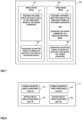
- Figure 7 schematically illustrates one example of a method for operating the power converter arrangement according to Figures 1 and 2 .
- the method 100 includes operating the power converter arrangement either in the single-phase mode 110 or the three-phase mode 120.
- operating the power converter arrangement in the single-phase mode includes receiving the same input voltage Vabc at each of the three input nodes a, b, c of the power converter 11 (111), and operating the buffer circuit 12 to regulate the output voltage Vqr of the buffer circuit 12 (112).
- Operating the power converter arrangement in the three-phase mode includes receiving different input voltages Va, Vb, Vc at the three input nodes a, b, c of the power converter 11 (121), and operating the buffer circuit 12 to regulate the output voltage Vxz of the power converter 11.
- regulating the output voltage Vxz of the power converter 11 is the same as regulating the input voltage of the buffer circuit 12.
- voltage Vxz is referred to as output voltage of the power converter 11 or as input voltage of the buffer circuit 12 in the following.
- the output nodes x, z of the power converter 11 are input nodes of the buffer circuit 12.
- nodes x, z are referred to as output nodes of the power converter 11 or as input nodes of the buffer circuit 12 in the following.
- Figure 8 illustrates a block diagram of the controller 13, which is configured to control operation of the power converter arrangement in accordance with the method illustrated in Figure 7 .
- the controller 13 includes four control units, a first control unit 131 (CON-1P) configured to control operation of the power converter (CON) 11 in the single-phase (1P) mode; a second control unit 132 (BLTF-1P) configured to control operation of the buffer circuit (BUF) 12 in the single-phase (1P) mode; a third control unit 133 (CON-3P) configured to control operation of the power converter (CON) 11 in the three-phase (3P) mode; and a fourth control unit 134 (BLTF-3P) configured to control operation of the buffer circuit (BUF) 12 in the three-phase mode (3P).
- the first, second, third, and fourth control units 13 1, 132, 133, 134 are also referred to as first, second, third, and fourth controllers in the following.
- Figure 8 illustrates the functionality of the controller 13 rather than a specific implementation.
- the controller 13 may be implemented in various ways.
- the controller 13 with the different control units 131, 132, 133, 134 can be implemented as a dedicated control circuit.
- the controller 13 includes a microcontroller, wherein the different control units are implemented as different program codes each configured to operate the microcontroller such that it has the functionality of the respective control unit.
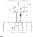
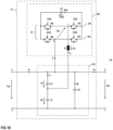
- FIG. 9 illustrates one example of the buffer circuit 12.
- the buffer circuit 12 includes a capacitor circuit 121 with a first capacitor 21 connected between output nodes x, z of the power converter 11 (not illustrated in Figure 9 ) wherein the output nodes x, z of the power converter 11 are also the input nodes of the buffer circuit 12.
- the capacitor circuit 121 further includes a second capacitor 22 connected between output nodes q, r of the buffer circuit 2, and a third capacitor 23.
- the third capacitor 23 is connected between the first capacitor 21 and the second capacitor 22 such that a series circuit including the first capacitor 21 and the third capacitor 23 is connected in parallel with the second capacitor 22.
- the first capacitor 21 is also referred to as input capacitor
- the second capacitor 22 is also referred to as output capacitor
- the third capacitor 23 is also referred to as control capacitor.
- the output voltage Vqr of the buffer circuit 12 is given by the voltage across the second capacitor 22. Furthermore, an input voltage Vxz of the buffer, which is the output voltage Vxz of the power converter 11 (not illustrated in Figure 9 ), equals a voltage Vd across the first capacitor 21.
- a second input node z of the buffer circuit 12, which is identical with a second output node of the power converter, and a second output node r of the buffer circuit 12 are directly connected, so that the output voltage Vqr is given by the input voltage Vxz plus a voltage Vf across the third capacitor 23.
- the output voltage Vqr can be regulated by suitably regulating the voltage Vf across the third capacitor 23.
- the capacitor circuit 21 of the buffer circuit 12 may further include a fourth capacitor 24 and a switchover switch 25 that is controlled by a drive signal S25 provided by the controller 13.
- the switchover switch 25 is configured to connect the fourth capacitor 24 in parallel with the first capacitor 21 (input capacitor of the buffer circuit 2) or in parallel with the second capacitor 22 (output capacitor of the buffer circuit 2).
- the fourth capacitor 24 in the single-phase operation, is connected in parallel with the first capacitor 21 in order to increase an input capacitance of the buffer circuit 12 and, in the three-phase operation, the fourth capacitor 24 is connected in parallel with the second capacitor 22 in order to increase an output capacitance of the buffer circuit 12.
- a capacitance of the fourth capacitor 24 is much higher than capacitances of the first, second, and third capacitors 21, 22, 23.
- the capacitance of the fourth capacitor 24 is between 50 times and 200 times the capacitance of each of the first, second, and third capacitors 21, 22, 23.
- the capacitance of each of the first, second, and third capacitors 21, 22, 23 is selected from between 3 microfarads ( ⁇ F) and 10 microfarads ( ⁇ F), and the capacitance of the fourth capacitor 24 is selected from between 200 ⁇ F and 600 ⁇ F.
- the buffer circuit 12 further includes a voltage regulator 122.
- the voltage regulator 122 is controlled by the controller 13 (not illustrated in Figure 9 ) and is configured to regulate the voltage Vf across the third capacitor (control capacitor) 23 in order to regulate the output voltage Vqr. More specifically, the voltage regulator 122 is controlled by the second control unit 132 of the controller 13. One example of the second control unit 132 is explained herein further below.
- the voltage regulator 122 includes an inductor 31, a buffer capacitor 32, and a bridge circuit 33 with a first half-bridge 34s and a second half-bridge 34t.
- Each of the first and second half-bridges 34s, 34t includes a first electronic switch 35s, 35t and a second electronic switch 36s, 36t connected in series, The series circuit including the first and second electronic switches 35s, 35t, 36s, 36t of each of the half bridges 34s, 34t is connected in parallel with the buffer capacitor 32.
- each of the first and second half bridges 34s, 34t includes a switched node s, t, which is a circuit node at which the respective first and second electronic switches 35s, 35t, 36s, 36t are connected.
- the switched node of one of the two half-bridges 34s, 34t is connected to one of the two circuit nodes of the third capacitor 23, and the switched node of the other one of the two half bridges 34s, 34t is connected to the other one of the two circuit nodes of the third capacitor 23.
- the inductor 31 is connected between the third capacitor 23 and the switched node of one of the two half-bridges 33, 34.
- the inductor 31 is connected between the switched node t of the second half-bridge 34t and a first circuit node of the third capacitor 23, wherein the first circuit node of the third capacitor 23 is the circuit node that is connected to a first output node q of the buffer circuit 12.
- the switched node s of the first half bridge 34s is connected to a second circuit node of the third capacitor 23, wherein the second circuit node of the third capacitor 23 is the circuit node connected to a first input node x of the buffer circuit 2 (which is a first output node of the power converter 11).
- the electronic switches 35s, 35t, 36s, 36t of the first and second half-bridges 34s, 34t may include a switching element and a rectifier element (freewheeling element) connected in parallel with the switching element.
- the electronic switches 35s, 35t, 36s, 36t are implemented as MOSFETs, wherein integrated body diodes of the MOSFETs form the freewheeling element. This, however, is only an example. Any other electronic switch with an integrated or external freewheeling element may be used as well.
- the voltage Vf across the third capacitor 23 is regulated by controlling the switched node voltage Vst. More specifically, the voltage Vf across the third capacitor 23 is regulated by controlling an average switched node voltage Vst_avg.
- the switched node voltage Vst is controlled by controlling operation of the bridge circuit 33.
- the bridge circuit 33 operates in a switched mode.
- operating the bridge circuit 33 in the switched mode includes operating the bridge circuit 33 in a plurality of successive drive cycles wherein, in each of the drive cycles, at least one of the first and second electronic switches of at least one of the first and second half-bridges 34s, 34t is switched on and off.
- the average switched node voltage Vst_avg is the switched node voltage Vst averaged over the duration of one or more drive cycles.
- the switched node voltage Vst of the bridge circuit 33 can be equal to the buffer voltage Vbuf, equal to the inverted buffer voltage -Vbuf, or zero.
- the buffer voltage Vbuf is the voltage across the buffer capacitor 32.
- the polarity (sign) and the voltage level of the average switched node voltage Vst_avg can be adjusted by suitably modulating the switched node voltage Vst between zero and the buffer voltage Vbuf or between zero and the inverted buffer voltage -Vbuf.
- the duty cycle d12 can be positive or negative, wherein the average switched node voltage Vst_avg is positive when the duty cycle d12 is positive and negative when the duty cycle is negative d12.
- the switching frequency f12 is in the range of between 20 kHz and 2 MHz, for example.
- the power converter 11 operates in a switched mode at a switching frequency.
- the switching frequency of the power converter 11 is fixed.
- the switching frequency of the voltage regulator 122 in the buffer circuit 12 is higher than the switching frequency of the power converter 11.
- the switching frequency of the voltage regulator 122 in the buffer circuit 12 is between 2 times and 5 times the switching frequency of the power converter 11, for example.
- an input current Ix received at the input x, z by the buffer circuit 12 essentially equals an output current Iq provided at the output q, r of the buffer circuit 12.
- This current flows through the voltage regulator 122, wherein a (small) portion of the input current Ix is used to charge the buffer capacitor 32, which provides the buffer voltage Vbuf.
- the buffer voltage Vbuf is also regulated or adjusted by the switched mode operation of the bridge circuit 33, which is explained herein further below.
- the voltage Vf across the third capacitor 23 is regulated by suitably controlling the switched node voltage Vst. More specifically, by suitably controlling the switched node voltage Vst, a capacitive current If into or from the third capacitor 23 is regulated in order to regulate the voltage Vf across the third capacitor 23.
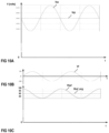
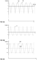
- Figures 10A-10C show signal diagrams that illustrate the operating principle of the buffer circuit 12 according to Figure 9 in the single-phase mode. More specifically, Figures 10A-10C show signal diagrams of the buffer circuit input voltage Vxz, the buffer circuit output voltage Vqr, the voltage Vf across the third capacitor 23, and the buffer voltage Vbuf over one period of the alternating input voltage Vabc (not illustrated in Figures 10A-10C ).
- the input voltage Vxz of the buffer circuit which is the output voltage of the power converter 11, includes voltage ripples that have a frequency that is twice the frequency of the input voltage Vabc. As explained above, this voltage ripples result from the input power Pin having a sine squared waveform.
- the output voltage Vqr is essentially constant.
- this is achieved by regulating the voltage Vf across the third capacitor 23 such that the voltage Vf across the third capacitor 23 includes voltage ripples of the same type as the input voltage Vxz but with a respective phase shift of 180°. "Of the same type” in this regard includes that the voltage ripples of the voltage Vf across the third capacitor 23 have the same frequency and amplitude as the voltage ripples of the input voltage Vxz.
- the input voltage Vxz plus the voltage Vf across the third capacitor 23 equals the output voltage Vqr.
- the capacitor voltage Vf compensates for the voltage ripples included in the input voltage Vxz, so that the output voltage Vqr is essentially constant.
- the voltage Vf across the third capacitor 23 is an alternating voltage, so that a DC offset is essentially zero.
- the output voltage Vqr equals an average of the input voltage Vxz.
- "Essentially zero" in this context means that the voltage Vf across the third capacitor 23 may include a low DC offset which is required for controlling the buffer voltage Vbuf and for compensating losses that may occur in the voltage regulator 122.
- the buffer capacitor 32 is periodically charged and discharged. More specifically, the buffer capacitor 32 is discharged when the third capacitor 23 is to be charged and the buffer capacitor 32 is charged when the third capacitor 23 is to be discharged. Consequently, the buffer voltage Vbuf includes voltage ripples that have essentially the same frequency as the voltage ripples of the input voltage Vxz'.
- the buffer voltage over one period of the alternating input voltage Vabc is illustrated in Figure 10C .
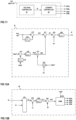
- FIG 11 shows a block diagram of one example of the second control unit 132 (BLTF-1P) that is configured to control operation of the buffer circuit 12 according to Figure 9 in the single-phase mode.
- the second control unit 132 includes a voltage controller 41 that is configured to output a capacitor current reference If ⁇ .
- the capacitor current reference If ⁇ represents a desired current level of a current If into the third capacitor 23 in order to achieve the desired voltage level of the voltage Vf across the third capacitor 23.
- the second control unit 132 includes a current controller 43.
- the current controller 43 receives the capacitor current reference If ⁇ and is configured to control operation of the voltage regulator 122 such that the current If into the third capacitor 23 at least approximately equals the capacitor current reference If ⁇ .
- the current controller 43 controls operation of the bridge circuit 33 by generating drive signals S35s, S35t, S36s, S36t that are received by the electronic switches 35s, 35t, 36s, 36t in the bridge circuit 33 and are configured to switch on or off the electronic switches 35s, 35t, 36s, 36t.
- FIG 12A illustrates a more detailed example of the voltage controller 41 illustrated in Figure 11
- Figure 12B illustrates a more detailed example of the current controller 43 illustrated in Figure 11 .
- the voltage controller 41 generates the capacitor current reference If ⁇ dependent on a measured input voltage Vxz' and a buffer voltage reference Vbuf ⁇ .
- the measured input voltage Vxz' represents the input voltage Vxz of the buffer circuit 12 and can be obtained by measuring the input voltage Vxz using a conventional voltage sensor.
- Voltage sensors are commonly known, so that no further explanation is required in this regard.
- measured voltage denotes a signal obtained by measuring a respective voltage.
- measured current denotes a signal obtained by measuring a respective current using a current sensor.
- the measured input voltage Vxz' is proportional to the input voltage Vxz.
- the input voltage Vxz of the buffer circuit 12 equals a voltage Vd across the first capacitor 21, so that the measured input voltage Vxz' equals a measured capacitor voltage Vd'.
- the voltage controller 41 generates a capacitor voltage reference Vf ⁇ , wherein the capacitor voltage reference Vf ⁇ represents a desired voltage level of the voltage Vf across the third capacitor 23.
- the capacitor voltage reference Vf ⁇ varies over one period of the alternating input voltage Vabc in order to obtain a voltage waveform of the capacitor voltage Vf as illustrated in Figure 10B .
- the capacitor voltage reference Vf ⁇ includes a first capacitor voltage reference Vf1 ⁇ and a second capacitor voltage reference Vf2 ⁇ that are added by an adder 411.
- the first capacitor voltage reference Vf1 ⁇ is dependent on the measured input voltage Vxz' and is a portion of the capacitor voltage reference Vf ⁇ that is required to generate the capacitor voltage Vf dependent on the input voltage Vxz such that the output voltage Vqr is essentially constant.
- the first capacitor voltage reference Vf1 ⁇ is generated to represent a 180° phase-shifted version of the voltage ripples included in the input voltage Vxz. This is achieved by low-pass filtering the inverted measured input voltage -Vxz' by a low-pass filter 412 and by subtracting the low-pass filtered measured input voltage from the inverted measured input voltage -Vxz' by a subtractor 413.
- the inverted measured input voltage -Vxz' instead of the measured input voltage Vxz' ensures that the first capacitor voltage reference Vf1 ⁇ has a phase shift of 180° relative to the voltage ripples included in the measured input voltage Vxz'.
- the output of the subcontractor 413 represents the 180° phase shifted voltage ripples included in the input voltage Vxz.
- the second capacitor voltage reference Vf2 ⁇ is dependent on the buffer voltage reference Vbuf ⁇ and is used to regulate the buffer voltage Vbuf such that the buffer voltage Vbuf or an average of the buffer voltage Vbuf essentially equals the buffer voltage reference Vbuf ⁇ .
- the buffer voltage reference Vbuf ⁇ has a predefined value, wherein the predefined value is selected such that the buffer voltage Vbuf is high enough to achieve an amplitude of the voltage across Vf across the third capacitor 23 that is at least the amplitude of the voltage ripples included in the input voltage Vxz in order to be able to compensate for such voltage ripples by adding the voltage Vf across the third capacitor 23 to the input voltage Vxz across the first capacitor 21.
- the voltage controller 41 generates a buffer voltage error by subtracting a low-pass filtered measured buffer voltage Vbuf' from the buffer voltage reference Vbuf ⁇ by a subtractor 414.
- the measured buffer voltage Vbuf' is obtained by measuring the buffer voltage Vbuf
- the low-pass filtered measured buffer voltage is obtained by low-pass filtering the measured buffer voltage Vbuf' by a low-pass filter 415.
- a controller 416 such as a proportional controller, provides a buffer capacitor current reference Ibuf ⁇ .
- the buffer capacitor current reference Ibuf ⁇ represents a desired current into the buffer capacitor 32, which is the current that is required to adjust the buffer voltage Vbuf such that it equals the buffer voltage reference Vbuf ⁇ .
- the second capacitor voltage reference Vf2 ⁇ is obtained by multiplying, using a multiplier 417, the buffer capacitor current reference Ibuf ⁇ with Vbuf ⁇ /-Iq', wherein Iq' denotes the measured output current.
- the quotient Vbuf ⁇ /-Iq' is provided by a divider 418 based on the capacitor voltage reference Vbuf ⁇ and the measured output current Iq'. The reason for this operation is briefly explained in the following.
- the current IL through the inductor 31 is "quasi" constant and equal to the inverted output current -Iq.
- the voltage controller 41 generates a capacitor voltage error by subtracting, by a subtractor 419, the measured voltage Vf' across the third capacitor 23 from the capacitor voltage reference Vf ⁇ of the third capacitor 23.
- a controller 420 such as a proportional controller, generates the capacitor current reference If ⁇ .
- the capacitor current reference If ⁇ represents the desired current into the third capacitor 23 that is required in order to achieve that the voltage Vf across the third capacitor 23 is in accordance with the capacitor voltage reference Vf ⁇ .
- the current controller 43 generates an inductor current reference IL ⁇ , which represents the desired current level of a current IL through the inductor 31 of the voltage regulator 22.
- Calculating the inductor current reference IL ⁇ includes, for example, adding the inverted capacitor current reference If ⁇ , and the inverted measured input current Ix' by an adder 431.
- a controller 432 such as a proportional controller generates an inductor voltage reference VL ⁇ based on a difference between the inductor current reference IL ⁇ and the measured inductor current IL'. This difference is provided by a subtractor 435, for example.
- the inductor voltage reference VL ⁇ represents the (average) voltage across the inductor 31 that is required in order to achieve an (average) current IL through the inductor that is in accordance with the inductor current reference IL ⁇ . Due to the switched mode operation of the bridge circuit 33 the current IL through the inductor 31 may vary.
- the average inductor current is the current through the inductor 31 averaged over the duration of at least one drive cycle of the bridge circuit 33.
- a subtractor 433 subtracts the measured voltage Vf' across the third capacitor 23 from the inductor voltage reference VL ⁇ in order to obtain a switched node voltage reference Vst ⁇ .
- the switched node voltage reference Vst ⁇ represents the (average) switched node voltage that is required in order to achieve a current through the inductor 31 that is in accordance in accordance with the inductor current reference IL ⁇ , so that the current If into the third capacitor 23 is in accordance with the capacitor current reference If ⁇ and so that the capacitor voltage Vf is in accordance with the capacitor voltage reference Vf ⁇ .
- a PWM modulator 434 receives the switched node voltage reference Vst ⁇ and operates the first and second half bridges 33, 34 such that the (average) switched node voltage Vst is in accordance with the switched node voltage reference Vst ⁇ . More specifically, the PWM modulator 434 generates the drive signals S35s, S35t, S36s, S36t that control operation of the first and second switches 35s, 35t, 36s, 36t of the bridge circuit 33.
- Each of these drive signals S35s, S35t, S36s, S36t switches on or switches off the respective electronic switch, wherein the PWM modulator 434 is configured to adjust the duty cycles of the drive signals S35s, S35t, S36s, S36t dependent on the switched node voltage reference Vst ⁇ and the measured buffer voltage Vbuf such that (as explained with reference to equations (2) to (4)) an average of the switched node voltage Vst at least approximately equals the switched node voltage reference Vst ⁇ .
- Figures 13A-13C show signal diagrams that illustrate the operating principle of the buffer circuit 12 according to Figure 9 in the three-phase mode. More specifically, Figures 13A-13C show signal diagrams of a buffer circuit input voltage reference Vxz ⁇ and a buffer circuit input voltage Vxz, the voltage Vf across the third capacitor 23, and the buffer voltage Vbuf over one period of the alternating input voltage Vabc (not illustrated in Figures 13A-13C ).
- the buffer circuit 12 regulates the voltage level of the input voltage Vxz, which is the output voltage of the power converter (PFC rectifier) 1, wherein regulating the input voltage Vxz of the buffer circuit 12 enables the PFC rectifier 1 to operate in the 1/3 mode.
- the input voltage reference Vxz ⁇ represents the desired voltage level of the input voltage Vxz.
- the buffer circuit 12 is configured to regulate the input voltage Vxz to be in accordance with the input/output voltage reference Vxz ⁇ .
- the voltage Vxz at the output of the PFC rectifier 11 has a six-pulse shape similar to the six-pulse shape of the maximum line-to-line voltage Vll.
- the voltage reference Vxz ⁇ is provided by the third control unit 133 that controls operation of the PFC rectifier 1 in the three-phase mode. This is explained herein further below.
- the output voltage Vqr of the buffer circuit 12 is regulated by the PFC rectifier 11. More specifically, the PFC rectifier 11 regulates an average input power such that the average input power essentially equals a power consumption of the load, so that the output voltage Vqr is essentially constant. As outlined above, In the three-phase mode, variations of the input power are much lower than in the single-phase mode, so that voltage ripples of the output voltage Vqr resulting from the varying input power are much lower in the three-phase mode than in the single-phase mode.
- the output voltage Vqr can be considered to be essentially constant, so that the input voltage Vxz of the buffer circuit, which is given by the output voltage Vqr minus the voltage Vf across the third capacitor 23, can be regulated by regulating the voltage Vf across the third capacitor 23.
- the buffer circuit 12 is controlled by the fourth control unit 134 to adjust the voltage Vf across the third capacitor 23 such that the capacitor voltage Vf essentially equals an inverted version of the six-pulse shaped voltage ripples included in the input voltage reference Vxz ⁇ .
- a signal waveform of the capacitor voltage Vf adjusted in this way is illustrated in Figure 13B .
- the buffer voltage Vbuf varies (oscillates) around the buffer voltage reference Vbuf ⁇ .
- the buffer voltage reference Vbuf ⁇ may be the same as in the single-phase mode.
- FIG 14 shows a block diagram of one example of the fourth control unit 134 (BUF-3P) that is configured to control operation of the buffer circuit 12 according to Figure 9 in the three-phase mode.
- the fourth control unit 134 includes a voltage controller 45 configured to output the capacitor current reference If ⁇ , and a current controller 47 configured to receive the capacitor current reference If ⁇ and to control operation of the voltage regulator 122 such that the current If into the third capacitor 23 at least approximately equals the capacitor current reference If ⁇ .
- the current controller 47 can be implemented in the same way as the current controller 43 illustrated in Figure 12B , so that with regard to the functionality of the current controller 47 reference is made to Figure 12B and the corresponding description.
- the voltage controller 45 is similar to the voltage controller 41 illustrated in Figure 12A and is configured to generate the capacitor voltage reference Vf ⁇ by adding, using an adder 451, a first capacitor voltage reference Vf1 ⁇ and a second capacitor voltage reference Vf2 ⁇ .
- a subtractor 459 in the same way as subtractor 419 according to Figure 12A , generates a capacitor voltage error by subtracting the measured capacitor voltage Vf' from the capacitor voltage reference Vf ⁇ .
- controller 460 which is a proportional controller, for example, generates the capacitor current reference If ⁇ based on the capacitor voltage error.
- the second capacitor voltage reference Vf2 ⁇ is generated in the same way as in the voltage controller 41 according to Figure 12A .
- the subtractor 454 corresponds to subtractor 414 in the voltage controller 41
- low-pass filter 455 corresponds low-pass filter 415
- controller 456 corresponds to controller 416
- multiplier 457 corresponds to multiplier 417
- divider 458 corresponds to divider 418.
- the second capacitor voltage reference Vf2 ⁇ is that portion of the capacitor voltage reference Vf ⁇ that is used to regulate the buffer voltage Vbuf.
- the first capacitor voltage reference Vf1 ⁇ which is usually much higher than the second capacitor voltage reference Vf2 ⁇ and dominates the capacitor voltage reference Vf ⁇ , is that portion of the capacitor voltage reference Vf ⁇ that is used to adjust the capacitor voltage Vf to be in accordance with the inverted voltage ripples included in the input voltage reference Vxz ⁇ .
- generating the first capacitor voltage reference Vf1 ⁇ includes subtracting the measured output voltage Vqr' from the input voltage reference Vxz ⁇ by a subtractor 461 in order to obtain a difference that represents the voltage ripples included in the input voltage reference Vxz ⁇ , and subtracting a low-pass filtered version of this difference from the difference by a further subtractor 453.
- a low-pass filter 452 generates the low-pass filtered difference. Subtracting the low-pass filtered difference from the difference removes a possible DC offset from the difference.
- Figure 16 illustrates a buffer circuit 12 with a capacitor circuit 121 and a voltage regulator 122 according to another example.
- the voltage regulator 122 is implemented in the same way as the voltage regulator 122 according to Figure 9 and includes an inductor 31, a bridge circuit 33, and a buffer capacitor 32.
- the capacitor circuit 121 is different from the capacitor circuit 121 according to Figure 8 in that the third capacitor 23 is connected in series with the first capacitor 21 between the input nodes x, z of the buffer circuit 12,.
- the voltage Vf across the third capacitor 23 is regulated by the voltage regulator 122.
- the first input node x and the first output node q of the buffer circuit 12 are directly connected, so that the load current Iq, different from the buffer circuit 12 according to Figure 9 , does not flow through the voltage regulator 122.
- the regulated voltage Vxz generated at the input of the buffer circuit is the same voltage as the output voltage Vqr, so that possible voltage ripples of this voltage Vxz also occur at the output q, r.
- Figures 17A-17C show signal diagrams that illustrate the operating principle of the buffer circuit 12 according to Figure 16 in the single-phase mode. More specifically, Figures 17A-17C show signal diagrams of the voltage Vd across the first capacitor 21, the voltage Vf across the third capacitor 23 connected in series with the first capacitor 21, the voltage Vbuf across the buffer capacitor 32, and the output voltage Vqr, which equals the input voltage Vxz.
- the voltage Vd across the first capacitor 21 includes voltage ripples. These voltage ripples result from the varying input power in the single-phase mode (see Figure 4 ). Without the voltage regulator 122 voltage ripples would occur both in the voltage Vd across the first capacitor 21 and the voltage Vf across the third capacitor 23. Amplitudes of the voltage ripples in the voltage Vd across the first capacitor 21 and the voltage Vf across the control capacitor 23 may be different and are dependent on the capacitances of the first and second capacitors 21, 23 that form a capacitive voltage divider. According to one example, the capacitance of the control capacitor 23 is much lower than the capacitance of the first capacitor 21.
- the capacitance of the control capacitor 23 is less than 10% or less than 5% of the capacitance of the first capacitor 21.
- Capacitances of the first and second capacitor 21, 22 may be in the same range as the capacitances of the first and second capacitors 21, 22 in the buffer circuit 12 according to Figure 16 .
- the voltage across the third capacitor 23 can be regulated such that this voltage Vf has a waveform that is different from the waveform resulting from the varying input power and counteracts voltage ripples occurring in the voltage Vf across the first capacitor 21.
- the voltage regulator 122 in combination with the control capacitor 23 fulfills two main tasks. First, the voltage regulator 122 generates the voltage Vf across the control capacitor 23 such that voltage ripples in the voltage Vd across the first capacitor 21 are essentially canceled out. Second, a current is injected into the first capacitor 21 that excites the first capacitor 21 to buffer voltage fluctuations resulting from the varying input power Pin.
- the voltage Vf across the third capacitor 23 is regulated such that the capacitor voltage Vf includes voltage ripples of the same type as the voltage Vd across the first capacitor 21 but with a phase shift of 180°. "Of the same type” in this regard includes that the voltage ripples of the voltage Vf across the third capacitor 23 have the same frequency and amplitude as the voltage ripples of the voltage Vd across the first capacitor 21. Referring to the above, the voltage Vd across the first capacitor 21 plus the voltage Vf across the third capacitor 23 equals the output voltage Vqr, so that the capacitor voltage Vf compensates for the voltage ripples included in the voltage Vd across the first capacitor 21 and the output voltage Vqr is essentially constant.
- the buffer voltage Vbuf varies over one period of the varying input voltage (not illustrated in Figures 7A-7C) as the capacitor voltage Vf varies.
- FIG 18 shows a block diagram of the second control unit 132 that is configured to control operation of the buffer circuit 12 illustrated in Figure 16 in the single-phase mode.
- This control unit 132 is in accordance with the second control unit 132 illustrated in Figure 11 .
- the control unit 132 includes a voltage controller 41 configured to provide the capacitor current reference If ⁇ , and a current controller 43 configured to receive the capacitor current reference If ⁇ and to drive the bridge circuit 33 in order to adjust the switched node voltage Vst.
- FIGS 19A, 19B Examples of the voltage controller 41 and the current controller 43 are illustrated in Figures 19A, 19B .
- the voltage controller 41 according to Figure 19A is based on the voltage controller 41 according to Figure 12A
- the current controller 43 according to Figure 19B is based on the current controller 43 according to Figure 12B .
- same parts as in the voltage controller 41 according to Figure 12A are labeled with the same reference numbers
- same parts as in the current controller 43 according to Figure 12B are labeled with the same reference numbers.
- the differences between the voltage controller 41 according to Figure 19A and the voltage controller according Figure 12A and the differences between the current controller 43 according to Figure 19B and the current controller according to Figure 12B are explained.
- the voltage controller 41 generates the capacitor voltage reference Vf ⁇ based on the measured voltage Vd' across the first capacitor 21 and the output voltage reference Vqr ⁇ . More specifically, a difference between the output voltage reference Vqr ⁇ and the measured capacitor voltage Vd' is generated by a subtractor 421. Low-pass filter 412 provides a low-pass filtered version of the difference, and subtractor 413 subtracts the low-pass filtered version of the difference from the difference in order to obtain the capacitor voltage reference Vf ⁇ . Further processing of the capacitor voltage reference Vf ⁇ in order to obtain the capacitor current reference If ⁇ is the same as in the voltage controller 41 according to Figure 12A .
- the voltage controller 41 In addition to the capacitor current reference If ⁇ , the voltage controller 41 according to Figures 18 and 19A generates a further current reference If_buf ⁇ . As explained with reference to Figure 19B , this further current reference If_buf ⁇ forms a portion of the inductor current reference IL ⁇ . More specifically, the further current reference If_buf ⁇ represents a portion of the desired current through the inductor 31 that is required to control the current Ibuf into the buffer capacitor 32 and, therefore, to control the buffer voltage Vbuf.
- generating the further current reference includes generating the buffer current reference Ibuf ⁇ based on the buffer voltage reference Vbuf ⁇ and the measured buffer voltage Vbuf as explained with reference to Figure 12A hereinabove.
- Generating the further current reference If_buf ⁇ further includes multiplying the buffer current reference Ibuf ⁇ with the buffer voltage reference Vbuf ⁇ using a multiplier 422 In order to obtain a buffer power reference Pbuf ⁇ , which represents a power to be received by the buffer capacitor 32 in order to achieve that the buffer voltage Vbuf essentially equals the buffer voltage reference Vbuf ⁇ .
- This buffer power reference Pbuf ⁇ is divided, using a divider 423, by the RMS value of the measured control capacitor voltage Vf'.
- the RMS value is provided by an RMS generator 424 that receives the measured control capacitor voltage Vf'.
- An output signal of the divider 423 is multiplied, by multiplier 425, with the measured control capacitor voltage Vf' in order to obtain the further current reference If_buf ⁇ .
- the further current reference If_buf ⁇ Due to multiplying the divider 423 Output signal with the measured control capacitor voltage Vf', the further current reference If_buf ⁇ is in phase with the voltage Vf across the control capacitor 23.
- an amplitude of this further current reference If_buf ⁇ is dependent on the buffer power reference Pbuf ⁇ .
- an inductor current reference IL ⁇ is generated based on the capacitor current reference If ⁇ .
- the inductor current reference IL ⁇ is processed in the same way as in the current controller 43 according to Figure 12B , in order to generate the switched node voltage reference Vst ⁇ and drive the bridge circuit 33.
- the current controller 43 according to Figure 19B is different from the current controller according to Figure 12B in the way the inductor current reference IL ⁇ is generated based on the capacitor current reference If ⁇ .
- the measured output current Iq' is subtracted from the measured input current Ix' by a subtractor 436 in order to obtain a first difference
- the control capacitor current reference If ⁇ is subtracted from the first difference by a further subtractor 437 in order to obtain a second difference.
- the control capacitor reference If ⁇ is generated by the voltage controller 41 as explained hereinabove.
- the further voltage reference If_buf ⁇ generated by the voltage controller 41 is added to the second difference by an editor 431 in order to obtain the inductor current reference IL ⁇
- Figures 20A-20C show signal diagrams that illustrate the operating principle of the buffer circuit 12 according to Figure 16 in the three-phase mode. More specifically, Figures 20A-20C show signal diagrams of the voltage Vd across the first capacitor 21, the voltage Vf across the third capacitor 23 connected in series with the first capacitor 21, the voltage Vbuf across the buffer capacitor 32, and the input voltage Vxz over one period of the alternating input voltage Vabc (not illustrated in Figures 20A-20C ). Referring to the above, in the buffer circuit 12 according to Figure 16 , the input voltage Vxz equals the output voltage Vqr.
- the buffer circuit 12 regulates the voltage level of the input voltage Vxz, which is the output voltage of the power converter (PFC rectifier) 1, wherein regulating the input voltage of the buffer circuit 12 enables the PFC rectifier 1 to operate in the 1/3 mode.
- the input voltage reference Vxz ⁇ represents the desired voltage level of the input voltage Vxz.
- the buffer circuit 12 is configured to regulate the input voltage Vxz to be in accordance with the input/output voltage reference Vxzv.
- the voltage Vxz at the output of the PFC rectifier 11 has a six-pulse shape similar to the six-pulse shape of the maximum line-to-line voltage Vll.
- the voltage reference Vxz ⁇ is provided by the third control unit 133 (CON-3P) that controls operation of the PFC rectifier 1 in the three-phase mode. This is explained herein further below.
- the voltage Vd across the first capacitor 21 is essentially constant, so that the input voltage Vxz with the six-pulse shape can be achieved by regulating the capacitor voltage Vf across the third capacitor 23 to have a six-pulse shape waveform.
- FIG 21 illustrates a block diagram of the fourth control unit 134 (BUF-3P) that is configured to control operation of the buffer circuit 12 according to Figure 16 in the three-phase mode.
- This control unit 134 is in accordance with the control unit 134 according to Figure 14 and includes a voltage controller 45 configured to generate a capacitor current reference If ⁇ and a current controller 47 configured to receive the capacitor current reference If ⁇ and drive the bridge circuit 33 in accordance with the capacitor current reference If ⁇ .
- FIG. 22 One example of the voltage controller 45 is illustrated in Figure 22 .
- the current controller 47 according to Figure 21 is in accordance with the current controller 43 according to Figure 19B , so that with regard to the current controller 47 reference is made to Figure 19B and the corresponding description.
- the voltage controller 45 illustrated in Figure 22 is very similar to the voltage controller 41 illustrated in Figure 19A and includes the same control topology as the voltage controller 41 illustrated in Figure 19A .
- subtractor 461 corresponds to subtractor 421 in Figure 19A
- low-pass filter 452 corresponds to low-pass filter 412
- subtractor 453 corresponds to subjective 413
- subtractor 459 corresponds to subtractor 419
- controller 460 corresponds to controller 420.
- the voltage controller 45 according to Figure 22 is different from the voltage controller 41 according to Figure 19A only in that the control capacitor reference If ⁇ is generated based on the output voltage reference Vxz ⁇ of the power converter 11 instead of the output voltage reference Vqr ⁇ of the buffer circuit 12. That is, subtractor 461 according to Figure 22 receives the output voltage reference Vxz ⁇ of the power converter 11, while subtractor 421 according to Figure 19A receives the output voltage reference Vqr ⁇ of the buffer circuit 12.
- the control loop for generating the further current reference If_buf ⁇ is identical with the corresponding control loop in the voltage controller 41 according to Figure 19A . That is, in the control loop according to Figure 22 , subtractor 454 corresponds to subtractor 414 in Figure 19A , low-pass filter 455 corresponds to low-pass filter 415, controller 456 corresponds to controller 416, multiplier 462 corresponds to multiplier 422, divider 463 corresponds to divider 423, RMS filter 464 corresponds to RMS filter 424, and multiplier 465 corresponds to multiplier 425.
- Figure 23 illustrates a modification of the buffer circuit 12 according to Figure 16 .
- the buffer circuit according to Figure 23 in the same way as in the buffer circuit according to Figure 16 , the first and third capacitors 21, 23 are connected in series between the input nodes x, z, and the second capacitor 22 is connected between the output nodes q, r of the buffer circuit 12.
- the buffer circuit according to Figure 23 includes a switchover switch 26 that is configured to connect the second capacitor 22 either in parallel with the first capacitor 21 or in parallel with the series circuit including the first and third capacitors 21, 23.
- the switchover switch 26 is controlled by the control circuit 13 (not illustrated in Figure 23 ), wherein the control circuit 13 is configured to operate the switchover switch 26 such that the second capacitor 22 is connected in parallel with the first capacitor 21 in the three-phase mode and is connected in parallel with the series circuit including the first and third capacitors 21, 23 in the single-phase mode.
- the buffer circuit 12 according to Figure 23 operates in the same way as the buffer circuit 12 according to Figure 16 in the single-phase mode.
- the voltage Vd across the first capacitor 21 equals the output voltage Vqr, which is essentially constant, and the input voltage Vxz is regulated by regulating the voltage Vf across the third capacitor 23 to have a waveform of the same type as the waveform illustrated in Figure 20B , so that the input voltage Vxz has a waveform of the type illustrated in Figure 20A .
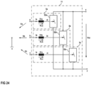
- the PFC rectifier 11 may be implemented in various ways. Different examples for implementing the PFC rectifier 11 are explained in the following. Basically, as illustrated in Figure 24 , the PFC rectifier 11 includes three rectifier stages 5a, 5b, 5c, which may also be referred to as rectifier branches or rectifier legs. Each rectifier stage 5a, 5b, 5c includes an inductor 51a, 52a, 52c connected between a respective one of the input nodes a, b, c and a respective switched node a ⁇ , b ⁇ , c ⁇ .
- Each of the switched nodes a ⁇ , b ⁇ , c ⁇ is connected to the output nodes x, z through a switching circuit 52a, 52b, 52c, wherein each of the switching circuits 52a, 52b, 52c includes at least one electronic switch.
- Regulating the input currents Ia, Ib, Ic includes regulating voltages VLa, VLb, VLc across the inductors 51a, 51b, 51c, wherein regulating the voltages VLa, VLb, VLc includes adjusting electrical potentials at the switched nodes a ⁇ , b ⁇ , c ⁇ .
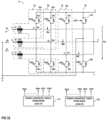
- FIG 25 illustrates one example of a PFC rectifier 11 in greater detail.
- each of the rectifier stages 5a, 5b, 5c has a totem pole topology.
- each of the switching circuits 52a, 52b, 52c includes a half-bridge with a first electronic switch 53a, 53b, 53c and a second electronic switch 54a, 54b, 54c that are connected in series between the output nodes x, z, wherein the output nodes x, y are the input nodes of the buffer circuit 12 (not illustrated in Figure 25 ).
- the switched node a ⁇ , b ⁇ , c ⁇ of each rectifier stage 5a, 5b, 5c is the circuit node at which the first and second switches 53a, 53b, 53c, 54a, 54b, 54c of the respective half-bridge are connected.
- the PFC rectifier 1 includes an unfolding bridge 55 with a first electronic switch 551 and a second electronic switch 552 that are connected in series between the output nodes x, z.
- a circuit node at which the first and second electronic switches 551, 552 are connected is connected to the reference node n of the input voltages Va, Vb, Vc.
- the unfolding bridge 55 is only in operation when the power converter 11 operates in the single-phase mode. In the three-phase mode, the unfolding bridge 55 is not active so that there is no circuit node in the power converter 11 that is connected to the reference node n in the three-phase mode. Furthermore, in the three-phase mode there is essentially no low frequency current into the reference node n.
- Low-frequency in this context means a frequency corresponding to the frequency of the input voltages Va, Vb, Vc or twice this frequency.
- the switching circuits 52a, 52b, 52c and the unfolding bridge 55 are operated by the first control unit 131 (CON-1P) in the single-phase mode and the third control unit 133 (CON-3P) in the three-phase mode.
- each of the first and third control units 131, 133 outputs drive signals S53a, S53b, S53c, S54a, S54b, S54c, S551, S552 received by the respective switches 53a, 53b, 53c, 54a, 54b, 54c, 551, 552.
- the switches 53a, 53b, 53c, 54a, 54b, 54c, 551, 552 may include a switching element and a rectifier element connected in parallel with the switching element. According to one example, the switches are implemented as MOSFETs. This, however, is only an example. Any other electronic switch with an integrated or external freewheeling element may be used as well.
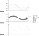
- Figures 26A-26C shows signal diagrams that illustrate operation of the PFC rectifier 11 according to Figure 25 in the single-phase mode.
- the rectifier stages 5a, 5b, 5c operate in the same way.
- Figures 26A-26C illustrate signal diagrams that illustrate operation of only the first rectifier stage 5a, that receives the first input voltage Va illustrated in Figure 26A and the first input current Ia illustrated in Figure 26B .
- a duty cycle da of a switched mode operation of the first rectifier stage 5a is illustrated in Figure 26C .
- the first rectifier stage 5a is operated such that the average input current Ia has the same waveform as the input voltage Va, which is a sinusoidal waveform in the example illustrated in Figures 26A and 26B .
- the rectifier stage 5a is operated in a switched mode. Due to the switched mode operation of the rectifier stage 5a the input current Ia varies around the average input current Ia_avg.
- Figure 26B illustrates the envelope of the input current Ia.
- the average input current Ia_avg (illustrated in the enlarged section illustrated in Figure 26B ) is in the middle of the envelope illustrated in Figure 26B .
- regulating the (average) input current Ia includes regulating an (average) voltage VLa across the inductor 51a.
- Regulating this voltage VLa includes regulating an electrical voltage Va ⁇ at the switched node a ⁇ by a switched mode operation of the switching circuit 52a with the first and second electronic switches 53a, 54a.
- the unfolding bridge 55 is operated by the first control unit 131 such that during a positive halfwave of the input voltage Va the second electronic switch 552, which is the electronic switch connected between the second output node z and the reference node n, is switched on and the first electronic switch 551, which is connected between the first output node x and the reference node n is switched off. Equivalently, during a negative halfwave of the input voltage Va, the first electronic switch 551 is switched on and the second electronic switch 552 is switched off.
- the switching circuit 52a is operated in a switched mode. This includes operating the switching circuit 52a in a plurality of drive cycles. In each of the drive cycles, one of the first and second electronic switches 53a, 54a operates as a control switch and the other one of the first and second electronic switches 53a, 54a operates as a commutation switch.
- the control switch is operated in a PWM (pulsewith modulated) fashion. Operating the control switch in a PWM fashion includes operating the control switch in a plurality of successive drive cycles having a duration T11, includes operating the control switch in an on-state (switched-on state) for an on-time Ton11 and an off-state (switched-off state) for an off time Toff11 in each drive cycle. During the on-time Ton11, the control switch conducts the input current Ia through the inductor 51a.
- the commutation switch takes over the input current.
- the commutation switch may be operated in a complementary PWM fashion, which includes operating the commutation switch in the off-state during the on-time Ton11 and in the on-state during off time Toff11.
- the commutation switch may be operated in an off-state throughout the time period in which the control switch is operated in a PWM fashion.
- the freewheeling element of the commutation switch takes over the current during the off time off the control switch Toff11.
- Operating the commutation element in the complementary PWM fashion helps to reduce switching losses as compared to operating the commutation switch in the off-state.
- the second electronic switch 54a is the control switch that is operated in the PWM fashion and the first electronic switch 53a is the commutation switch.
- the first electronic switch 53a is the control switch that is operated in the PWM fashion and the second electronic switch 54a is the commutation switch.
- the switched node voltage Va ⁇ is zero when the control switch is switched on and essentially equals either the output voltage Vxz or the inverted output voltage -Vxz when the control switch is switched off.
- the switched node voltage Va ⁇ equals the output voltage Vxz when the control switch is switched off
- the switched node voltage equals the inverted output voltage -Vxz when the control switch is switched off.
- Va ⁇ Toff 11
- T 11 ⁇ Vxz 0.5 ⁇ da + 1 ⁇ Vxz
- Va ⁇ Toff 11
- T 11 ⁇ ⁇ Vxz 0.5 ⁇ ⁇ da + 1 ⁇ ⁇ Vxz
- Toff11 denotes the off-time of the control switch.
- da denotes a duty cycle of operating the rectifier stage 5a.
- One example of the duty cycle is illustrated in Figure 26C .
- the duty cycle ranges between -1 and +1.
- the sign of the duty cycle da indicates which of the first and second switches 53a, 54a has its on-time Ton11 and off-time Toff11 defined by equations (5a) and (5b), wherein the other one of the first and second switches is operated in a complementary fashion.
- a negative sign of the duty cycle indicates that the on-time Ton11 and the off-time Toff11 of the second switch 54a is defined by equations (5a) and (5b)
- a positive sign of the duty cycle indicates that the on-time Ton11 and the off time Toff11 of the first switch 53a is defined by equations (5a) and (5b).
- a duty cycle of the rectifier stage 5a of -1 means that the second switch 54a is switched on and the first switch 53a is switched off throughout the drive cycle; a duty cycle of +1 means that the first switch 53a is switched on and the second switch 54a is switched off throughout the drive cycle; a duty cycle of 0 means that each of the first switch 53a and the second switch 54a is switched on 50% of the drive cycle; a duty cycle of -0.5 means that the second switch 54a is switched on 75% of the drive cycle and the first switch 53a is switched on 25% of the drive cycle; and a duty cycle of 0.5 means that the first switch 53a is switched on 75% of the drive cycle and the second switch 54a is switched on 25% of the drive cycle.
- the drive cycle da increases towards the middle of the positive halfwave and, in the present example, is positive in the middle of the positive halfwave. This includes that the first switch 53a is switched on longer than the second switch 54a in drive cycles in the middle of the positive halfwave. In other words, the duration of the off time of the second switch 54a increases towards the middle of the positive halfwave.
- the drive cycle da decreases towards the middle of the negative halfwave and, in the present example, is negative in the middle of the negative halfwave. This includes, that the second switch 54a is switched on longer than the first switch 53a in drive cycles in the middle of the positive halfwave. In other words, the duration of the off time of the first switch 53a increases towards the middle of the positive halfwave.
- the duration T11 of the individual drive cycles is fixed, so that the rectifier stages operate at a fixed switching frequency.
- the fixed switching frequency is selected from between 20 kHz and 2 MHz, for example.
- Duty cycles db, dc of the rectifier stages 5b, 5c can be calculated based on respective switched node voltage references Vb ⁇ ⁇ , Vc ⁇ ⁇ in the same way.
- Figure 27 illustrates one example of the first control unit 131 (CON-1P) that is configured to control operation of the PFC rectifier 11 according to Figure 25 in the single-phase mode.
- the first control unit 131 includes a voltage controller 61 that is configured to generate input current references Ia ⁇ , Ib ⁇ , Ic ⁇ , wherein each of these input current references represents a desired average input current at the respective input node a, b, c.
- the input currents Ia, Ib, Ic may vary.
- Average input current in this context means the average of the respective input current over the duration of at least one drive cycle of the switched mode operation.
- input current denotes the average input current
- measured input current denotes the measured average input current.
- the first control unit 131 further includes a current controller 63, that receives the input current references Ia ⁇ , Ib ⁇ , Ic ⁇ and controls operation of the rectifier stages 5a, 5b, 5c. More specifically, the current controller 63 controls operation of the switching circuits 52a, 52b, 52c by generating the respective drive signals S53a, S53b, S53c, S54a, S54b, S54c received by the switches in the switching circuits 52a, 52b, 52c.
- An unfolding controller 65 controls operation of the unfolding bridge 55 in the way explained above, that is, by switching on the second switch 552 during the positive half wave and switching on the first switch 551 during the negative halfwave of the input voltage Va.
- Figure 28A illustrates one example of the voltage controller 61 according to Figure 27, and Figure 28B illustrates one example of the current controller 63 according to Figure 27 .
- the voltage controller 61 generates a conductance reference G ⁇ , which represents a desired input conductance of the PFC rectifier 11.
- Each of the input current references Ia ⁇ , Ib ⁇ , Ic ⁇ is generated by multiplying, using a respective multiplier 616a, 660b, 660c, the conductor current reference G ⁇ by the respective measured input voltage Va', Vb', Vc'.
- calculating the conductance reference includes subtracting, by a subtractor 611, the measured output voltage Vqr' of the power converter arrangement, which is the measured output voltage Vqr' of the buffer second 12, from an output voltage reference Vqr ⁇ .
- the output voltage reference Vqr ⁇ is a predefined value that defines a desired voltage level of the output voltage Vqr received by the load Z or the further power converter 14.
- a controller 612 such as a proportional controller, calculates the output capacitor reference Iqr ⁇ explained above.
- the output capacitor reference Iqr ⁇ represents a desired current into the second capacitor (output capacitor) 22 that is required in order to ensure that the output voltage Vqr at least approximately equals the output voltage reference Vqr ⁇ .
- An adder 613 adds the output capacitor reference Iqr ⁇ and the measured output current Iq', wherein the result represents an overall current that is to be provided by the PFC rectifier 11 at the circuit node at which the output capacitor 22 is connected to the output q.
- a multiplier 614 multiplies this overall current with the measured output voltage Vqr' in order to obtain an input power reference Pin ⁇ .
- the input power reference Pin ⁇ represents an average of the input power Pin over one period of the alternating input voltage that is required in order to achieve that the output voltage Vqr at least approximately equals the output voltage reference Vqr ⁇ .
- This input power reference Pin ⁇ is divided by 3 2 V 2 , where V denotes the amplitude of the input voltage Vabc, in order to obtain the conductance reference G ⁇ .
- the current controller 63 includes a PWM modulator 634 that receives the switched node voltage references Va ⁇ ⁇ , Vb ⁇ ⁇ , Vc ⁇ ⁇ and the measured output voltage Vxz' and is configured to generate the drive signals S53a, S54a, S53b, S54b, S53c, S54c received by the electronic switches in the switching circuit 52a, 52b, 52c such that the average switched node voltages are adjusted in accordance with equations (5a) and (5b) explained hereinabove.
- the current controller 63 includes three controller branches, wherein each of these controller branches is configured to provide one of the three switched node voltage references Va ⁇ ⁇ , Vb ⁇ ⁇ , Vc ⁇ ⁇ .
- a first controller branch that is configured to generate the first switched node voltage Va ⁇ ⁇ based on the first input current reference Ia ⁇ is briefly explained in the following.
- the other two controller branches are implemented and operated in the same way.
- like parts are labeled with the same reference signs that are different by added character "a" in the first controller branch, "b” and the second controller branch, and "c" in the third controller branch.
- the first controller branch includes an adder 631a that subtracts the measured first input current Ia' from the first input current reference Ia ⁇ to obtain an input current error.
- a controller 632a such as a proportional controller, generates an inductor voltage reference VLa ⁇ based on the input current error.
- the inductor voltage reference VLa ⁇ represents the desired average voltage across the first inductor 51a that is required in order to achieve that the first input current at least approximately equals the first input current reference Ia ⁇ .
- the switched node voltage Va ⁇ ⁇ reference is given by the measured first input voltage Va' (which equals the measured input voltage Vabc' in the single-phase mode) minus the inductor voltage reference VLa ⁇ and is provided by a subtractor 633a that receives the measured input voltage Va' and the inductor voltage reference VLa ⁇ .
- Figures 29A-29C show signal diagrams that illustrate operation of the PFC rectifier 11 according to Figure 25 in the three-phase mode.
- Figure 29A shows signal diagrams of the three different input voltages Va, Vb, Vc
- Figure 29B illustrates envelopes of the input currents Ia, Ib, Ic
- Figure 29C shows duty cycles da, db, dc of switched mode operations (PWM operations) of the rectifier stages 5a, 5b, 5c.
- the unfolding bridge 55 is deactivated. That is, the first and second electronic switches 551, 552 of the unfolding bridge 55 are switched off, so that none of the circuit nodes of the power converter 11 that are active in the three-phase mode is connected to the reference node n.
- the common mode voltage Vcm is the voltage between a virtual midpoint of the output nodes x, z and the reference node n to which the input voltages Va, Vb, Vc are referenced to.
- the duty cycles da, db, dc may vary between -1 and +1. These duty cycles define the on-times and the off times of the first switch 53a, 53b, 53c and the second switch 54a, 54b, 54c in each of the rectifier stages 5a, 5b, 5c in the same way as explained with regard to the duty cycle da and the first and second switches 53a, 54a in the single-phase hereinabove.
- a duty cycle of -1 means that the respective second switch 54a, 54b, 54c is switched on and the respective first switch 53a, 53b, 53c is switched off throughout a respective drive cycle;
- a duty cycle of +1 means that the respective second switch 54a, 54b, 54c is switched off and the respective first switch 53a, 53b, 53c is switched on throughout a respective drive cycle;
- a duty cycle of 0 means that each of the respective first switch 53a, 53b, 53c and the respective second switch 54a, 54b, 54c is switched on 50% of the respective drive cycle.
- the first and second rectifier stages5a, 5b are statically operated as long as the second input voltage Vb is the highest voltage and the first input voltage is the lowest voltage.
- the third and first rectifier stages 5c, 5a are statically operated and the second rectifier stage 5b is operated in the switched mode.
- FIG 30 illustrates one example of the third control unit 133 (CON-3P) that is configured to control operation of the PFC rectifier 11 according to Figure 25 in the three-phase mode.
- the third control unit 133 includes a voltage controller 66 that is configured to generate the input current references Ia ⁇ , Ib ⁇ , Ic ⁇ , wherein each of these input current references Ia ⁇ , Ib ⁇ , Ic ⁇ represents a desired average input current at the respective input node a, b, c.
- the input currents Ia, Ib, Ic may vary.
- Average input current in this context means the average of the respective input current over the duration of at least one drive cycle of the switched mode operation.
- input current denotes the average input current
- measured input current denotes the measured average input current.
- the third control unit 133 further includes a current controller 68, that receives the input current references Ia ⁇ , Ib ⁇ , Ic ⁇ and controls operation of the rectifier stages 5a, 5b, 5c. More specifically, the current controller 63 controls operation of the switching circuits 52a, 52b, 52c by generating the respective drive signals S53a, S53b, S53c, S54a, S54b, S54c received by the switches in the switching circuits 52a, 52b, 52c.
- An unfolding controller 70 controls operation of the unfolding bridge 55 in the way explained above, that is, by deactivating the unfolding bridge 55, wherein deactivating the unfolding bridge 55 includes switching off both the first switch 551 and the second switch 552 throughout the three-phase mode.
- the third control unit 133 outputs an output voltage reference Vxz ⁇ , which represents the desired voltage Vxz at the output of the PFC rectifier 11 and the input of the buffer circuit 12.
- Figure 31A illustrates one example of the voltage controller 66 according to Figure 30
- Figure 31B illustrates one example of the current controller 68 according to Figure 30
- the implementation and the functionality of the voltage controller 66 according to Figure 31A is the same as the implementation and the functionality of the voltage controller 61 according to Figure 28A , so that reference to the description of Figure 28A is made.
- subtractor 661 corresponds to subtractor 611 in Figure 28A
- controller 662 corresponds to controller 612
- adder 663 corresponds to adder 613
- multiplier 664 corresponds to multiplier 614
- divider 665 corresponds to divider 615
- multipliers 666a, 666b, 666c correspond to multipliers 616a, 616b, 616c.
- the current controller 68 according to Figure 31B is based on the current controller 63 according to Figure 28B .
- the current controller 68 according to Figure 31B includes three controller branches, wherein each of these controller branches outputs a respective one of the switched node voltage references Va ⁇ ⁇ , Vb ⁇ ⁇ , Vc ⁇ ⁇ to a PWM modulator 684.
- the PWM modulator in addition to the switch node voltage references Va ⁇ ⁇ , Vb ⁇ ⁇ , Vc ⁇ ⁇ receives the measured output voltage Vxz' and the common mode voltage Vcm and is configured to control operation of the switching circuits 52a, 52, 52c in accordance with equations (6a)-(6c) such that the average switched node voltages Va ⁇ , Vb ⁇ , Vc ⁇ equal the switched node voltage references Va ⁇ ⁇ , Vb ⁇ ⁇ , Vc ⁇ ⁇ .
- the common mode voltage Vcm is provided by a common mode voltage calculator 686 that receives the switched node voltage references Va ⁇ *, Vb ⁇ *, Vc ⁇ * and is configured to obtain (calculate) the common mode voltage reference Vcm* based on the switched node voltage references Va ⁇ *, Vb ⁇ *, Vc ⁇ * as explained with reference to equations (8a) and (8b) hereinabove.
- Each of the three controller branches is in accordance with the three controller branches in the current controller 63 according to Figure 28B . That is, in the current controller 68 according to Figure 31B , subtractors 681a, 681b, 681c correspond to subtractors 631a, 631b, 631c in the current controller 63 according to Figure 28B , controllers 682a, 682b, 682c correspond to controllers 632a, 632b, 632c, and subtractors 683a, 683b, 683c correspond to subtractors 633a, 633b, 633c.
- the current controller 68 furthermore includes a maximum/minimum selector that receives the switched node voltage references Va ⁇ ⁇ , Vb ⁇ ⁇ , Vc ⁇ ⁇ and selects a highest one of these switched node voltage references Va ⁇ ⁇ , Vb ⁇ ⁇ , Vc ⁇ ⁇ as a maximum switched node voltage reference Vmax ⁇ ⁇ and a lowest one of these switched node voltage references Va ⁇ ⁇ , Vb ⁇ ⁇ , Vc ⁇ ⁇ as a minimum switched node voltage reference Vmin ⁇ ⁇ .
- a subtractor 686 calculates the difference between the maximum and the minimum switched node voltage references Vmax ⁇ ⁇ , Vmin ⁇ ⁇ in order to provide the output voltage reference Vxz ⁇ .
- Generating the output voltage reference Vxz ⁇ in this way ensures that at each time the voltage Vx at the first output node x equals the desired switched node voltage at one of the switched nodes a ⁇ , b ⁇ , c ⁇ and the voltage Vz at the second output node z equals the desired switched node voltage at another one of the switched nodes a ⁇ , b ⁇ , c ⁇ .
- the (average) inductor voltages VLa, VLb, VLc are rather low as compared to the amplitudes of the input voltages Va, Vb, Vc, so that each of the switched node voltages Va ⁇ , Vb ⁇ , Vc ⁇ essentially follows the respective input voltages Va, Vb, Vc.
- the maximum switched node voltage reference Vmax ⁇ ⁇ essentially equals the highest one of the three input voltages Va, Vb, Vc
- the minimum switched node voltage reference Vmin ⁇ ⁇ essentially equals the lowest one of the three input voltages Va, Vb, Vc.
- the rectifier stage receiving the highest input voltage is operated in the static mode with a duty cycle of +1
- the rectifier stage receiving the lowest input voltage is operated in the static mode with a duty cycle of -1
- the rectifier stage receiving the intermediate input voltage which is the input voltage between the highest and the lowest input voltage, is operated in the PWM mode with a duty cycle of between -1 and +1.
- FIG 32 illustrates a modification of the PFC rectifier 11 according to Figure 25 .
- the PFC rectifier 11 according to Figure 32 has a Vienna rectifier topology. Different from the PFC rectifier 11 with the totem pole topology according to Figure 25 , the PFC rectifier 11 according to Figure 32 includes a midpoint y. Furthermore, each of the rectifier stages 5a, 5b, 5c, in addition to the first switch 53a, 53b, 53c and the second switch 54a, 54b, 54c includes a third electronic switch 56a, 56b, 56c connected between the respective switched node a ⁇ , b ⁇ , c ⁇ and the midpoint y.
- the first and third controllers 131, 133 control operation of each of the electronic switches 53a-56c in the rectifier stages 5a, 5b, 5c and the switches 551, 552 in the unfolding bridge 52.
- Figures 33A-33C shows signal diagrams that illustrate operation of the PFC rectifier 11 according to Figure 32 in the single-phase mode.
- the signal diagrams according to Figures 33A-33C correspond to the signal diagrams illustrated in Figures 26A-26C .
- Operation of the PFC rectifier 11 according to Figure 32 in the single-phase mode corresponds to operation of the PFC rectifier 11 according to Figure 25 in the single-phase mode, which includes that the first controller 131 according to Figure 32 , for controlling operation of the first switches 53a, 53b, 53c and the second switches 54a, 54b, 54c is implemented in the same way as the first controller 131 according to Figures 27 and 28A-28B . Additionally, the first controller 131 according to Figure 32 is configured to deactivate (switch off) the third switches 56a, 56b, 56c in the single-phase mode. Thus, in the single-phase mode, only the first and second switches of the rectifier stages 5a, 5b, 5c are operated in a switched-mode.
- Figures 34A-34C show signal diagrams that illustrate operation of the PFC rectifier 11 according to Figure 32 in the three-phase mode. These signal diagrams correspond to the signal diagrams illustrated in Figures 29A-29C .
- Operation of the PFC rectifier 11 according to Figure 32 in the three-phase mode is very similar to operation of the PFC rectifier 11 according to Figure 25 in the three-phase mode.
- the third controller 133 according to Figure 32 is very similar to the third controller 133 according to Figures 30 and 31A-31B .
- the voltage controller 66 (not illustrated in Figures 32 ) is implemented in accordance with the example illustrated in Figure 31A .
- One example of the voltage controller 68 included in the third controller 133 according to Figure 32 is illustrated in Figures 35 .
- the voltage controller 68 according to Figure 35 is based on the voltage controller 68 according to Figure 31B and has the same topology and includes the same functional blocks (functional units).
- the voltage controller 68 according to Figures 35 is different from the voltage controller according to Figures 31B in that the PWM circuit 684, in addition to generating the control signals control signals S53a, S54a, S53b, S54b, S53c, S54c for controlling operation of the first and second switches 53a, 54a, 53b, 54b, 53c, 54c, generates drive signals S56a, S56b, S56c for controlling operation of the third switches 56a, 56b, 56c.
- the functionality of the PWM circuit 684 according to Figure 35 is different from the functionality of the PWM circuit 684 according to Figure 31B as briefly explained in the following.
- the PWM circuit according to Figures 35 is configured to calculate the duty cycles da, db, dc of the rectifier stages 5a, 5b, 5c in accordance with equations (7a)-(7c) hereinabove.
- of the duty cycles da, db, dc, in each drive cycle define the on-time duration of the respective third switch 56a, 56b, 56c.
- the PWM circuit 684 is configured to generate the drive signals S56a, S56b, S56c such that the on-time durations of the third switches 56a, 56b, 56c are in accordance with the magnitudes of the duty cycles da, db, dc. More specifically, the PWM circuit 684 adjusts the on-time durations as being given by the magnitude of the respective duty cycle multiplied with the duration of the duty cycle.
- the first and second switches 53a, 53b, 53c, 54a, 54b, 54c may permanently be switched off in the three-phase mode, so that, in each rectifier stage 5a, 5b, 5c, the rectifier element of one of the first and second switches 53a, 53b, 53c, 54a, 54b, 54c takes over the respective inductor current Ia, Ib, Ic when the respective third switch 56a, 56b, 56c is in the off-state.
- the PWM circuit 684 according to Figures 34 only generates the third drive signals 56a, 56b, 56c.
- one of the first and second switches 53a, 53b, 53c, 54a, 54b, 54c in each drive cycle is operated in a complementary fashion to the respective third switch 56a, 56b, 56c.
- the respective first switch 53a, 53b, 53c is operated complementarily to the third switch 56a, 56b, 56c when the respective switched node voltage reference Va ⁇ ⁇ , Vb ⁇ ⁇ , Vc ⁇ ⁇ is positive (which is when the respective duty cycle da, db, dc is positive), and the respective second switch 54a, 54b, 54c is operated complementarily to the third switch 56a, 56b, 56c when the respective switched node voltage reference Va ⁇ ⁇ , Vb ⁇ ⁇ , Vc ⁇ ⁇ is negative (which is when the respective duty cycle da, db, dc is negative).
- the PWM circuit 684 is configured to generate drive signals for each of the switches S54a-S56c in each of the rectifier stages 5a, 5b, 5c.
- Figure 36 illustrates one example of a buffer circuit 12 that is configured to be connected to a 3-level PFC rectifier, such as the PFC rectifier 11 with the Vienna rectifier topology according to Figure 32 .
- the buffer circuit 12 is connected to the output nodes x, z and the midpoint y of the PFC rectifier (not illustrated in Figure 36 ).
- the buffer circuit 12 according to Figure 36 includes two input capacitors 21x, 21z and two output capacitors 22q, 22r.
- the buffer circuits 12 includes two control capacitors 23q, 23r.
- a first capacitor series circuit including the first output capacitor 22q and the first control capacitor 23q are connected between the first output node q and the midpoint y
- a second capacitor series circuit including the second control capacitor 23r and the second output capacitor 22r is connected between the midpoint y and the second output node r.
- the first and second capacitor series circuits are connected between the first output node q and the second output node r such that the first and second control capacitors 23q, 23r are connected at the midpoint y.
- the first input node x (which is identical with the first output node of the PFC rectifier) is directly connected to the first output node q
- the second input node z (which is identical with the second output node of the PFC rectifier) is directly connected to the second output node r.
- the buffer circuit 12 includes to switchover switches 27x, 27z.
- a first one 27x of these switches 27x, 27z is configured to connect the first input capacitor 21x either in parallel with the first output capacitor 22q, or in parallel with the first capacitor series circuit 22q, 23q.
- a second one 27z of these switches 27x, 27z is configured to connect the second input capacitor 21z either in parallel with the second output capacitor 22r or in parallel with the second capacitor series circuit 22r, 23r.
- the switchover switches 27x, 27z are controlled by the control circuit 13 such that in the single-phase mode the first and second input capacitors 21x, 21z are connected in parallel with the first and second capacitor series circuits, respectively. This is illustrated in Figure 36 .
- control circuit 13 controls the switch over switches 27x, 27z such that the first and second input capacitors 21x, 21z are connected in parallel with the first and second output capacitors 22q, 22r, respective. This is illustrated in Figure 38 and explained further below.
- the buffer circuit 12 further includes a voltage regulator 122 that is configured to regulate voltages Vfq, Vfr across the first and second control capacitors 23q, 23r.
- the voltage regulator 122 is similar to the voltage regulators 122 explained before and includes a buffer capacitor 32, a bridge circuit 33, and three inductors 31u, 31v, 31w.
- the bridge circuit 33 includes three half-bridges 34u, 34v, 34w that each include a first electronic switch 35u, 35v, 35w and a second electronic switch 36u, 36v, 36w connected in series with the first electronic switch 35u, 35v, 35w, wherein the series circuits are connected in parallel with the buffer capacitor 32.
- Each of the half-bridges 34u, 34v, 34w includes a switched node u, v, w that is connected to a respective one of the three inductors 31u, 31v, 31w.
- the inductors 31u, 31v, 31w are connected to the control capacitors 23q, 23r, so that by suitably controlling inductor currents ILu, ILv, ILw through the inductors 31u, 31v, 31w currents Ifq, Ifr into the control capacitors 23q, 23r can be controlled in order to regulate the voltages Vfq, Vfr across the control capacitors 23q, 23r.
- a first inductor 31u is connected between the switched node u of a first half-bridge 34u and the circuit node at which the first output capacitor 22q and the first control capacitor 23q are connected
- a second capacitor 31v is connected between the switched node v of a second half bridge 34 v and the circuit node at which the first and second control capacitors 23q, 23r are connected
- a third inductor 31w is connected between the switched node w of a third half-bridge 34w and the circuit node at which the second control capacitor 23r and the second output capacitor 22r are connected.
- the current through each of the inductors 31u, 31v, 31w can be controlled by controlling the voltages at the respective switched nodes u, v, w in the way explained herein before.
- a first further power converter 14q may be connected to the first output capacitor 22q, and a second further power converter 14r may be connected to the second output capacitor 22r.
- Each of these further power converters 14q, 14r can be an isolated power converter.
- Outputs of the further power converters 14q, 14r can be connected in parallel to a load Zo, such as a battery.
- Figures 37A-37D show signal diagrams that illustrate operation of the buffer circuit 12 according to Figure 36 in the single-phase mode. More specifically, Figures 37A-37D shows signal diagrams of the voltage Vqr between the output nodes q, r, of the voltage Vq across the first output capacitor 22q plus the voltage Vr across the second output capacitor 22r, of the voltages Vx, Vz across the first and second input capacitors 21x, 21z, of the voltages Vfq, Vfr across the control capacitors 23q, 23r, and of the buffer voltage Vbuf.
- the output voltage Vxz provided by the PFC rectifier 11 varies due to the varying input power. Consequently, the voltage Vqr between the output nodes q, r (which equals the output voltage Vxz) and the voltages Vx, Vz across the input capacitors 21x, 21z vary.
- the control capacitors 23q, 23r compensate for such variations. For this, referring to Figures 37B and 37C the voltages across the control capacitors 23q, 23r are regulated such that these voltages are alternating voltages with the same frequency and amplitude as the voltage ripples included in the input voltage Vxz. Consequently, the first and second output voltages Vq, Vr are essentially constant.
- the voltage Vx across the first input capacitor 21x equals the voltage Vxy between the first input node x and the midpoint y. Furthermore, the voltage Vz across the second input capacitor 21z equals the voltage Vyz between the midpoint y and the second input node z.
- Figure 38 illustrates operation of the buffer circuit 12 according to Figure 36 in the three-phase node.
- the input capacitors 21x, 21z are connected in parallel with the output capacitors 22q, 22r.
- the voltage Vxy between the first input node x and the midpoint y is regulated by regulating the voltage Vfq across the first control capacitor 23q
- the voltage Vyz between the midpoint y and the second input node z is regulated by regulating the voltage Vfr across the second control capacitor 23r.
- Figures 39A-39D show signal diagrams that illustrate operation of the buffer circuit 12 according to Figure 38 in the three-phase mode. More specifically, Figures 39A-39D show signal diagrams of the voltage Vqr between the output nodes q, r (which equals the voltage Vxz between the input nodes x, z), of the voltages Vq, Vx across the parallel circuit with the first input capacitor 21x and the first output capacitor 22q, of the voltages Vr, Vz across the parallel circuit with the second input capacitor 21z and the second output capacitor 22r, of the voltages Vfq, Vfr across the control capacitors 23q, 23r, and of the buffer voltage Vbuf.
- Figures 40 and 41 show a modification of the buffer circuit 12 according to Figure 36 .
- the buffer circuit 12 according to Figure 40 is different from the buffer circuit 12 according to Figure 36 in that the first and second control capacitors 23q, 23r are connected between the first and second input capacitors 21x, 21z, wherein the first control capacitor 23q is connected between the first input capacitor 21x and the midpoint y and the second control capacitor 23r is connected between the midpoint y and the second input capacitor 21z.
- the crossover switches 27x, 27z are controlled by the control circuit 13 (not illustrated in Figures 40 and 41 ).
- the first crossover switch 27x is configured to connect the first output capacitor 22q in parallel with the first input capacitor 21x or in parallel with a first capacitor series circuit including the first input capacitor 21x and the first control capacitor 23q.
- the second crossover switch 27z is configured to connect the second output capacitor 22r either parallel with the first input capacitor 21z or in parallel with a second capacitor series circuit including the second control capacitor 23r and the second input capacitor 21z.
- the control circuit 13 controls the crossover switches 27x, 27z, to connect the first output capacitor 22q in parallel with the first capacitor series circuit and to connect the second output capacitor 22r in parallel with the second capacitor series circuit.
- the voltage across the first output capacitor 22q is regulated to be essentially constant by regulating the voltage Vfq across the first control capacitor 23q
- the voltage across the second output capacitor 22r is regulated to be essentially constant by regulating the voltage Vfr across the second control capacitor 23r.
- the voltages across the first and second control capacitors 23q, 23r can be regulated by suitably controlling the inductor currents ILu, ILv, ILw.
- the control circuit 13 controls the crossover switches 27x, 27z to connect the first output capacitor 22q in parallel with the first input capacitor 21x and to connect the second output capacitor 22r in parallel with the first input capacitor 21z.
- the voltage Vxz between the first and second input nodes x, z is regulated by regulating the voltages Vfr, Vfq across the control capacitors 23q, 23r.
- Example 1 A method including: selecting from operating a power converter arrangement in a single-phase mode or a three-phase mode, wherein the power converter arrangement includes: a power converter having three input nodes each configured to receive a respective input voltage, and an output; and a buffer circuit connected to the output of the power converter, wherein operating the power converter arrangement in the single phase mode includes: receiving the same input voltage at each of the three input nodes of the power converter; and operating the buffer circuit to regulate at least one output voltage of the buffer circuit, and wherein operating the power converter arrangement in the three-phase mode includes: operating the buffer circuit to regulate at least one output voltage at the output of the power converter such that the power converter is enabled to operate in a reduced switching mode; and operating the power converter in the reduced switching mode.
- Example 2 The method according to claim 1, wherein the reduced switching mode is a 1/3 mode.
- Example 3 The method of claim 1 or 2, wherein the buffer circuit includes a capacitor circuit with at least one control capacitor, and wherein to regulate the at least one output voltage of the buffer circuit in the single-phase mode and to regulate the output of the power converter in the three-phase mode includes to regulate a voltage across the at least one control capacitor.
- Example 4 The method of claim 3, wherein the buffer circuit further includes: an input capacitor coupled between a first output node and a second output node of the power converter; and an output capacitor connected between a first output node and a second output node of the buffer circuit.
- Example 5 The method of claim 4, wherein the control capacitor is connected between the first output node of the power converter and the first output node of the buffer circuit.
- Example 6 The method of claim 5, wherein the method further includes: connecting a further capacitor in parallel with the input capacitor in the single-phase mode; and connecting the further capacitor in parallel with the output capacitor in the three-phase mode.
- Example 7 The method of claim 4, wherein the control capacitor is connected in series with the input capacitor between the first output node and the second output node of the power converter.
- Example 8 The method of claim 7, wherein the method further includes: in the single-phase mode, connecting the output capacitor in parallel with the series circuit including the input capacitor and the control capacitor, and in the three-phase mode, connecting the output capacitor in parallel with the input capacitor.
- Example 9 The method of any one of claims 1 to 8, wherein the power converter is a 2-level PFC rectifier.
- Example 10 The method of any one of claims 1 to 8, wherein the power converter is a 3-level PFC rectifier and includes a first output node, a second output node, and a midpoint.
- the power converter is a 3-level PFC rectifier and includes a first output node, a second output node, and a midpoint.
- Example 11 The method of claim 3, wherein the at least one control capacitor includes a first control capacitor coupled between the first output node and the midpoint and a second control capacitor coupled between the midpoint and the second output node, wherein the capacitor circuit further includes a first input capacitor connected to the first output node, a second input capacitor connected to the second output node, a first output capacitor, and a second output capacitor, and wherein the at least one output voltage includes a first output voltage across the first output capacitor and a second output voltage across the second output capacitor.
- Example 12 The method of claim 11, wherein the buffer circuit further includes: a first capacitor series circuit including the first output capacitor and the first control capacitor connected in series between the first output node and the midpoint, a second capacitor series circuit including the second output capacitor and the second control capacitor connected in series between the midpoint and the second output node, wherein operating the power converter arrangement in the single-phase mode includes connecting the first input capacitor in parallel with the first capacitor series circuit and the second input capacitor in parallel with the second capacitor series circuit, and wherein operating the power converter arrangement in the three-phase mode includes connecting the first input capacitor in parallel with the first output capacitor and the second input capacitor in parallel with the second output capacitor.
- Example 13 The method of claim 11, wherein the buffer circuit further includes: a first capacitor series circuit including the first input capacitor and the first control capacitor connected in series between the first output node and the midpoint, a second capacitor series circuit including the second input capacitor and the second control capacitor connected in series between the midpoint and the second output node, wherein operating the power converter arrangement in the single-phase mode includes connecting the first output capacitor in parallel with the first capacitor series circuit and the second output capacitor in parallel with the second capacitor series circuit, and wherein operating the power converter arrangement in the three-phase mode includes connecting the first input capacitor in parallel with the first output capacitor and the second input capacitor in parallel with the second output capacitor.
- Example 14 The method of any one of the preceding claims, wherein the power converter includes three rectifier stages that are each configured to be operated in a switched mode, wherein operating the power converter in the reduced switching mode includes operating only one of the three rectifier stages in the switched node and operating the remainder of the rectifier stages statically in a predefined operating state.
- Example 15 The method of claim 14, wherein operating only one of the three rectifier stages in the switched mode and operating the remainder of the rectifier stages statically includes operating the one of the three rectifier stages in the switched mode and operating the remainder of the rectifier stages statically for a plurality of successive drive cycles, wherein in each drive cycle and operating state of the one of the three rectifier stages changes at least once.
- Example 16 A control circuit, configured to operate a power converter arrangement including a power converter and a buffer circuit in a single-phase mode or a three-phase mode, wherein to operate the power converter arrangement in the single-phase mode includes: to operate the buffer circuit to regulate at least one output voltage of the buffer circuit, and wherein operating the power converter arrangement in the three-phase mode includes: to operate the buffer circuit to regulate at least one output voltage at the output of the power converter such that the power converter is enabled to operate in a reduced switching mode; and to operate the power converter in the reduced switching mode.
- Example 17 An executable program code including instructions which, when executed by a control circuit including a microcontroller, to cause the control circuit to carry out the method of any one of claims 1 to 15.
Landscapes
- Engineering & Computer Science (AREA)
- Power Engineering (AREA)
- Rectifiers (AREA)
Abstract
A method for operating a power converter, a control circuit for operating a power converter, and an executable program code are disclosed. The method includes selecting from operating a power converter arrangement in a single-phase mode or a three-phase mode. The power converter arrangement includes a power converter (11) having three input nodes (a, b, c) each configured to receive a respective input voltage (Va, Vb, Vc), and an output (x, z), and a buffer circuit (12) connected to the output (x, z) of the power converter (11). Operating the power converter arrangement in the single phase mode includes receiving the same input voltage (Vabc) at each of the three input nodes (a, b, c) of the power converter (11), and operating the buffer circuit to regulate at least one output voltage of the buffer circuit (12) Operating the power converter arrangement in the three-phase mode includes operating the buffer circuit (12) to regulate at least one output voltage (Vxz; Vx, Vz) at the output (x, z) of the power converter (11) such that the power converter (11) is enabled to operate in a reduced switching mode, and operating the power converter (11) in the reduced switching mode.
Description
- This disclosure relates in general to a power converter arrangement with a power converter, in particular a PFC rectifier, and a buffer circuit.
- One example relates to a method. The method includes operating a power converter arrangement in a single-phase mode or a three-phase mode. The power converter arrangement includes a power converter having three input nodes each configured to receive a respective input voltage, and an output. Furthermore, the power converter arrangement includes a buffer circuit connected to the output of the power converter. Operating the power converter arrangement in the single phase mode includes receiving the same input voltage at each of the three input nodes of the power converter, and operating the buffer circuit to regulate at least one output voltage of the buffer circuit. Operating the power converter arrangement in the three-phase mode includes operating the buffer circuit to regulate an output voltage at the output of the power converter such that the power converter is enabled to operate in a reduced switching mode, operating the power converter in the reduced switching mode.
- Examples are explained below with reference to the drawings. The drawings serve to illustrate certain principles, so that only aspects necessary for understanding these principles are illustrated. The drawings are not to scale. In the drawings the same reference characters denote like features.
-
Figure 1 illustrates one example of a power converter arrangement that includes a power converter configured to receive three input voltages and a buffer circuit connected to an output of the power converter; -
Figure 2 illustrates a power converter arrangement of the type illustrated inFigure 1 that further includes a further power converter connected to an output of the buffer circuit; -
Figure 3 shows a signal diagram of an input voltage received by the power converter arrangement in a single-phase mode; -
Figure 4 shows a signal diagram of an input power received by the power converter arrangement in the single-phase mode; -
Figure 5 shows signal diagrams of input voltages received by the power converter arrangement in a three-phase mode; -
Figure 6 illustrates a signal diagram of an input power received by the power converter arrangement in the three-phase mode; -
Figure 7 illustrates one example of a method for operating the power converter arrangement in the single-phase mode or the three-phase mode; -
Figure 8 illustrates one example of a control circuit (controller) of the power converter arrangement, wherein the control circuit includes a first, second, third, and fourth control unit; -
Figure 9 illustrates a circuit diagram of one example of the buffer circuit; -
Figures 10A-10C show signal diagrams that illustrate operation of the buffer circuit according toFigure 9 in the single-phase mode; -
Figure 11 illustrate one example of a control unit configured to control operation of the buffer circuit according toFigure 9 in the single-phase mode; -
Figures 12A-12B illustrate examples of a voltage controller and a current controller of the control unit according toFigure 11 ; -
Figures 13A-13C show signal diagrams that illustrate operation of the buffer circuit according toFigure 9 in the three-phase mode; -
Figure 14 illustrates one example of a control unit configured to control operation of the buffer circuit according toFigure 9 in the three-phase mode; -
Figure 15 illustrates one example of a voltage controller of the control unit according toFigure 14 ; -
Figure 16 illustrates a circuit diagram of another example of the buffer circuit; -
Figures 17A-17C show signal diagrams that illustrate operation of the buffer circuit according toFigure 16 in the single-phase mode; -
Figure 18 illustrates one example of a control unit configured to control operation of the buffer circuit according toFigure 16 in the single-phase mode; -
Figures 19A-19B illustrate examples of a voltage controller and a current controller of the control unit according toFigure 18 ; -
Figures 20A-20C show signal diagrams that illustrate operation of the buffer circuit according toFigure 16 in the three-phase mode; -
Figure 21 illustrates one example of a control unit configured to control operation of the buffer circuit according toFigure 16 in the three-phase mode; -
Figure 22 illustrates one examples of a voltage controller of the control unit according toFigure 21 ; -
Figure 23 illustrates a buffer circuit according to another example; -
Figure 24 schematically illustrates one example of the power converter; -
Figure 25 illustrates one example of a power converter of the type illustrated inFigure 24 that includes a totem pole topology; -
Figures 26A-26C show signal diagrams that illustrate operation of the power converter according toFigure 25 in the single-phase mode; -
Figure 27 illustrates one example of a control unit configured to control operation of the power converter according toFigure 24 in the single-phase mode; -
Figures 28A-28B illustrate examples of a voltage controller and a current controller included in the control unit according toFigure 27 ; -
Figures 29A-29C show signal diagrams that illustrate operation of the power converter according toFigure 25 in the three-phase mode; -
Figure 30 illustrates one example of a control unit configured to control operation of the power converter according toFigure 25 in the three-phase mode; -
Figures 31A-31B illustrate examples of a voltage controller and a current controller included in the control unit according toFigure 30 ; -
Figure 32 illustrates one example of a power converter of the type illustrated inFigure 24 that includes a Vienna rectifier topology; -
Figures 33A-33C show signal diagrams that illustrate operation of the power converter according toFigure 32 in the single-phase mode; -
Figures 34A-34C show signal diagrams that illustrate operation of the power converter according toFigure 31 in the three-phase mode; -
Figure 35 illustrates one example of a voltage controller included in the control circuit of the power converter according toFigures 32 ; -
Figure 36 illustrates one example of a buffer circuit configured to be connected to a power converter of the type illustrated inFigure 32 and operating in the single-phase mode; -
Figures 37A-37D show signal diagrams that illustrate operation of the buffer circuit according toFigure 36 in the single-phase mode; -
Figure 38 illustrates the buffer circuit according toFigure 36 operating in the three-phase mode; -
Figures 39A-39D show signal diagrams that illustrate operation of the buffer circuit according toFigure 36 in the three-phase mode; -
Figure 40 illustrates another example of a buffer circuit configured to be connected to a power converter of the type illustrated inFigure 32 and operating in the single-phase mode; and -
Figure 41 illustrates the buffer circuit according toFigure 40 operating in the three-phase mode. - In the following detailed description, reference is made to the accompanying drawings. The drawings form a part of the description and for the purpose of illustration show examples of how the invention may be used and implemented. It is to be understood that the features of the various embodiments described herein may be combined with each other, unless specifically noted otherwise.
-
Figure 1 illustrates one example of a power converter arrangement. The power converter arrangement includes apower converter 11 and abuffer circuit 12. Thepower converter 11 includes three input nodes a, b, c and an output x, z. Each of the input nodes a, b, c is configured to receive a respective input voltage Va, Vb, Vc. The input voltages Va, Vb, Vc are referenced to a reference node n, for example. Thebuffer circuit 12 is connected to the output x, z of thepower converter 11 and is configured to provide a buffer circuit output voltage Vqr at an output q, r of thebuffer circuit 12. In the example illustrated inFigure 1 , the output voltage Vqr of thebuffer circuit 12 is the output voltage of the power converter arrangement. The output voltage Vqr of the power converter arrangement may be received by a load Zo (illustrated in dashed lines), for example. - Optionally, an input filter (not illustrated) is connected between the input nodes a, b, c and the
power converter 11. As outlined below, thepower converter 11 is a switched-mode power converter, so that input currents Ia, Ib, Ic received by thepower converter 11 from the individual input nodes a, b, c may include current ripples. The input filter is configured to filter the input currents Ia, Ib, Ia so that the currents received from the input nodes a, b, c are essentially devoid of current ripples. An input filter of this type is commonly known, so that no further explanation is required in this regard input filter. - Furthermore, the power converter arrangement includes a control circuit (controller) 13 that is configured to control operation of the power converter arrangement. More specifically, the controller is configured to control operation of the
power converter 11 and thebuffer circuit 12. - According to another example illustrated in
Figure 2 , the power converter arrangement includes afurther power converter 14 connected to the output q, r of thebuffer circuit 12. Thefurther power converter 14 is configured to receive the output voltage Vqr provided by thebuffer circuit 12 and is configured to power a load Zo connected to an output of thefurther power converter 14 based on the output voltage Vqr and an output current Iq received from thebuffer circuit 12. The load Zo is a battery, for example. Thefurther power converter 14 may be configured to regulate at least one of a current Izo provided to the load Zo or a voltage Vzo across the load Zo. - According to one example, the
further power converter 14 is an isolated power converter, which is a power converter that provides for a galvanic isolation between an input and an output of the furtherpower converter number 14. The input of thefurther power converter 14 is connected to the output q, r of thebuffer circuit 12, and the output of thefurther power converter 14 is connected to the load Zo. The galvanic isolation between the input and the out output may be implemented using a transformer or may be implemented using capacitors, for example. - As illustrated, the power converter arrangement may include a
further controller 15 that is configured to control operation of thefurther power converter 14. Thepower converter 13 and thefurther power converter 15 may share the same resources, such as a microcontroller executing program code for controlling thepower converter 11, thebuffer circuit 12, and thefurther power converter 14. - The
power converter 11 according toFigures 1 and 2 is configured to operate in a PFC (power factor correction) mode and, therefore, may also be referred to as PFC rectifier. In thePFC rectifier 11, the input currents Ia, Ia b, Ic received at the inputs a, b, c are regulated dependent on the input voltages Va, Vb, Vc in order to control the power factor. More specifically, the waveforms of the input currents Ia, Ib, Ic are regulated to have the same waveform as the input voltages Va, Vb, Vc. The input currents Ia, Ib, Ic can be regulated such that the waveform of each of the input currents Ia, Ib, Ic is in phase with the respective input voltage Va, Vb, Vc, or such that there is a phase shift between the input current Ia, Ib, Ic and the respective input voltage Va, Vb, Vc. - As outlined below, the input voltages Va, Vb, Vc are alternating input voltages, so that the input currents Ia, Ib, Ic are alternating input currents. An average input power received by the
PFC rectifier 11 can be controlled by controlling amplitudes of the input currents Ia, Ib, Ic, which is also explained herein further below. - Due to the switched-mode operation of the
PFC rectifier 11, the input currents Ia, Ib, Ic may include current ripples. However, unless specifically stated otherwise, input currents Ia, Ib, Ic as used herein denote average input currents. In this context, an "average input current" is an input current averaged over one or more drive cycles of the switched-mode operation of thePFC rectifier 11. - Operating the power converter arrangement includes selecting from operating the power converter arrangement in a single-phase mode or a three-phase mode. Referring to
Figure 3 , operating the power converter arrangement in the single-phase mode includes receiving the same input voltage Vabc at each of the three input nodes a, b, c, so that Vabc = Va = Vb = Vc. The input voltage Vabc is a sinusoidal input voltage with a frequency of 50 hertz (Hz) or 60 Hz, for example. An RMS (root mean square) value of the input voltage Vabc may range between 100 VRMS and 300 VRMS and is 230 VRMS or 110 VRMS, for example. The amplitude of the input voltages Vabc is
-
Figure 3 illustrates a signal diagram of a sinusoidal input voltage Vabc during one period. Just for the purpose of illustration, the input voltage illustrated inFigure 3 is a sinusoidal voltage having an RMS value of 230VRMS and an amplitude of 325V. The input voltage Vabc is a single-phase voltage received from a power grid, for example. -
Figure 4 illustrates the input power Pin and the average input power Pin_avg of the PFC rectifier operated in the single-phase mode. The input power Pin is given by
Figure 4 illustrates the input power Pin over one period of the input voltage Vabc. For the purpose of illustration it is assumed that thepower converter 11 operates in the PFC mode such that the input currents Ia, Ib, Ic each have the same waveform as the input voltage Vabc and are in phase with the input voltage Vabc, so that the input currents Ia, Ib, Ic are sinusoidal input currents in phase with the sinusoidal input voltage Vabc. In this case, as illustrated inFigure 4 , the waveform of the input power Pin is a sine squared waveform having twice the frequency of the frequency of the input voltage Vabc. - A conventional power converter operating as a PFC rectifier includes an output capacitor connected to the output of the power converter. If, for example, the output capacitor is charged to reach a predefined voltage level at startup and a load draws a constant power from the power converter that equals the average input power Pin_avg the voltage across the output capacitor has a voltage ripple that is in accordance with the varying input power.
- Referring to
Figure 5 , operating the power converter (PFC rectifier) 11 in the three-phase mode includes receiving different input voltages Va, Vb, Vc at the three input nodes a, b, c. According to one example, each of the three input voltages Va, Vb, Vc is a sinusoidal input voltage, wherein the input voltages Va, Vb, Vc have the same frequency and RMS value. The frequency is 50 Hz or 60 Hz, the RMS value is 230 VRMS or 110 VRMS, for example. The input voltages Va, Vb, Vc are different by having different phase angles. According to one example, a phase shift between each pair of the input voltages Va, Vb, Vc is 120° (2π/3). Just for the purpose of illustration, the input voltages Va, Vb, Vc illustrated inFigure 5 are sinusoidal voltages with an RMS value of 230VRMS and an amplitude of 325V. The input voltages Va, Vb, Vc are voltages received from a three-phase power grid, for example. - Furthermore, operating the
PFC rectifier 11 in the three-phase mode includes regulating the input current Ia, Ib, Ic received at each of the input nodes a, b, c such that the waveform of the respective input current Ia, Ib, Ic equals the waveform of the respective input voltage Va, Vb, Vc. - In the three-phase mode, each pair of the input voltage Va, Vb, Vc defines a line-to-line voltage, which is given by the difference of the two input voltages included in the respective pair. The line-to-line voltage is the voltage between each pair of the input nodes a, b, c illustrated in
Figures 1 and 2 , so that there are three line-to-line voltages Vab, Vbc, Vca (and three inverted line-to-line voltages Vba, Vcb, Vac). In a power converter arrangement that receives sinusoidal input voltages, the line-to-line voltages also have sinusoidal waveforms with the same frequency as the input voltages Va, Vb, Vc. In an input voltage system with 230VRMS sinusoidal input voltages Va, Vb, Vc, for example, the amplitude of the line-to-line voltages is 563V. - At each time during one period of the input voltages Va, Vb, Vc one of the three line-to-line voltages has the highest magnitude (absolute value). At time instance t1 illustrated in
Figure 5 , for example, the line-to-line voltage having the highest magnitude is line voltage Vab (=Va-Vb), and at time instance t2, for example, the line-to-line voltage having the highest magnitude is line voltage Vca (=Vc-Va). In the following, "highest line-to-line voltage" is the voltage that is given by the line-to-line voltage having the highest magnitude. The highest line-to-line voltage Vll is also illustrated inFigure 5 . The highest line-to-line voltage, during one period of the input voltages Va, Vb, Vc includes six pulses, so that the waveform of the highest line-to-line voltage has a six-pulse shape and is a six-pulse waveform. - When operating the
PFC rectifier 11 in the three-phase mode the input power Pin received by the PFC rectifier is essentially constant. This is illustrated inFigure 6 , which illustrates the input power of thePFC rectifier 11 operated in the three-phase mode. Different from operating thePFC rectifier 11 in the single-phase mode, in the three-phase mode, the input power Pin does not decrease to zero. Voltage ripples that may occur in the input power Pin due to the six-pulse shape of the highest line-to-line voltage and a corresponding six-pulse shape of the overall input current, are not illustrated inFigure 6 and are much lower than in the single-phase mode. Thus voltage ripples that may occur at the output of a conventional PFC rectifier that is operated in the three-phase mode are much lower than in the single-phase mode. - Basically, in the three-phase mode, the
PFC rectifier 11 can be operated in a normal operating mode or a reduced switching mode. ThePFC rectifier 11 includes three rectifier branches (rectifier legs). The rectifier branches are not illustrated inFigures 1 and 2 and are explained in detail herein further below. Each of the rectifier branches is connected between a respective one of the input nodes a, b, c and the output nodes x, z. - In the normal operating mode, which may also be referred to as 3/3 mode, each of the rectifier branches operates in a switched mode, which includes operating the rectifier branches in a plurality of successive drive cycles. The latter may include that one or more switches included in the respective rectifier branch are switched on and off at least once during a respective drive cycle, so that an operating state of the rectifier branches (rectifier stage) changes at least one in a respective drive cycle. A PFC rectifier operating in the normal mode is not only configured to regulate waveforms of the input currents but is also configured to regulate an output voltage of the PFC rectifier such that the output voltage is a direct voltage with a predefined voltage level.
- The reduced switching mode is a 1/3 mode, for example. In the 1/3 mode, only one of the rectifier branches is operated in the switched mode, while the other two rectifier branches are statically operated. "To statically operate" may include to operate an electronic switch included in the respective rectifier branch in a predefined operating state for a plurality of successive drive cycles, that is, for a certain time period that is much longer than the time period of one drive cycle of the switched-mode operation. The rectifier stage that is operated in the switched mode changes several times throughout one period of the input voltages Va, Vb, Vc. According to one example, which one of the rectifier stages is operated in the switched mode is dependent on a relationship between the input voltages Va, Vb, Vc. According to one example, the rectifier stage that receives the intermediate input voltage is operated in the switched mode. The "intermediate input voltage" is that one of the input voltages that is between the other two input voltages. That is, at each time one of the three input voltages is the highest input voltage, one of the three input voltages is the lowest input voltage, and the intermediate input voltage is that one of the input voltages that is between the highest and the lowest input voltage.
- As compared to operating the
PFC rectifier 11 in the normal mode, switching losses that occur in thePFC rectifier 11 can be reduced in the 1/3 mode, so that the efficiency of operating thePFC rectifier 11 is higher in the 1/3 mode than in the normal operating mode. In the 1/3 mode, thePFC rectifier 11 is configured to regulate the input currents Ia, Ib, Ic. However, in the 1/3 mode, thePFC rectifier 11 is not capable of regulating the output voltage Vxz to be a direct voltage with a predefined voltage level. Instead, in order to be able to operate in the 1/3 mode, a waveform of the output voltage of the PFC rectifier is to be regulated by an electronic circuit different from thePFC rectifier 11. - Selecting from operating the power converter arrangement in the single-phase mode or the three-phase mode may include monitoring the input voltages Va, Vb, Vc and may include operating the power converter (PFC rectifier) 11 in the single-phase mode when the input voltages Va, Vb, Vc are identical and operating the
power converter 11 in the three-phase mode when the input voltages are three different (phase shifted) alternating input voltages. - According to another example, selecting from operating the power converter arrangement in the single-phase mode or the three-phase mode includes receiving a mode selection signal by the
control circuit 13 and operating thepower converter 11 in the single-phase mode or the three-phase mode dependent on the selection signal. The selection signal can be any kind of signal that is suitable to enable thecontroller 13 to select between the two operating modes of thepower converter 11. According to one example, the selection signal is a signal manually input by a human user. According to another example, the selection signal is automatically generated by a sensor that is configured to detect whether the power converter arrangement is connected to a three-phase power grid or a single phase power grid. According to one example, the sensor is configured to detect the type of plug that is used to connect the power converter arrangement to the power grid. - In a conventional power converter arrangement with a PFC rectifier, a power converter connected downstream the PFC rectifier is configured to regulate the output voltage of the PFC rectifier in order to enable the PFC rectifier to operate in the 1/3 mode.
- In the power converter arrangement according to
Figures 1 and 2 , thebuffer circuit 12 is synergetically controlled by thecontroller 13 such that thebuffer circuit 12, - (a) in the single-phase mode, regulates the buffer circuit output voltage Vqr, and
- (b) in the three-phase mode regulates the output voltage Vxz of the
PFC rectifier 11. - According to one example, regulating the buffer circuit output voltage Vqr in the single phase mode includes regulating the output voltage Vqr such that it is essentially constant and does not include voltage ripples resulting from the alternating input power received by the
PFC rectifier 11 in the single phase mode. -
Figure 7 schematically illustrates one example of a method for operating the power converter arrangement according toFigures 1 and 2 . Referring toFigure 7 , themethod 100 includes operating the power converter arrangement either in the single-phase mode 110 or the three-phase mode 120. Referring toFigure 7 , and as explained before, operating the power converter arrangement in the single-phase mode includes receiving the same input voltage Vabc at each of the three input nodes a, b, c of the power converter 11 (111), and operating thebuffer circuit 12 to regulate the output voltage Vqr of the buffer circuit 12 (112). Operating the power converter arrangement in the three-phase mode includes receiving different input voltages Va, Vb, Vc at the three input nodes a, b, c of the power converter 11 (121), and operating thebuffer circuit 12 to regulate the output voltage Vxz of thepower converter 11. - It should be noted that regulating the output voltage Vxz of the
power converter 11 is the same as regulating the input voltage of thebuffer circuit 12. Thus, voltage Vxz is referred to as output voltage of thepower converter 11 or as input voltage of thebuffer circuit 12 in the following. Equivalently, the output nodes x, z of thepower converter 11 are input nodes of thebuffer circuit 12. Thus, nodes x, z are referred to as output nodes of thepower converter 11 or as input nodes of thebuffer circuit 12 in the following. - Examples of the method according to
Figure 7 are explained in the following with reference to different examples of thebuffer circuit 12 and thepower converter 11. PFC rectifiers that are capable of operating in a single phase mode or a three-phase mode are basically known, so that the focus of the following explanation is on thebuffer circuit 12 and its operating principle. -
Figure 8 illustrates a block diagram of thecontroller 13, which is configured to control operation of the power converter arrangement in accordance with the method illustrated inFigure 7 . Referring toFigure 8 , thecontroller 13 includes four control units, a first control unit 131 (CON-1P) configured to control operation of the power converter (CON) 11 in the single-phase (1P) mode; a second control unit 132 (BLTF-1P) configured to control operation of the buffer circuit (BUF) 12 in the single-phase (1P) mode; a third control unit 133 (CON-3P) configured to control operation of the power converter (CON) 11 in the three-phase (3P) mode; and a fourth control unit 134 (BLTF-3P) configured to control operation of the buffer circuit (BUF) 12 in the three-phase mode (3P). The first, second, third, andfourth control units 13 1, 132, 133, 134 are also referred to as first, second, third, and fourth controllers in the following. - It should be noted that
Figure 8 illustrates the functionality of thecontroller 13 rather than a specific implementation. Thecontroller 13 may be implemented in various ways. According to one example, thecontroller 13 with thedifferent control units controller 13 includes a microcontroller, wherein the different control units are implemented as different program codes each configured to operate the microcontroller such that it has the functionality of the respective control unit. -
Figure 9 illustrates one example of thebuffer circuit 12. Thebuffer circuit 12 includes acapacitor circuit 121 with afirst capacitor 21 connected between output nodes x, z of the power converter 11 (not illustrated inFigure 9 ) wherein the output nodes x, z of thepower converter 11 are also the input nodes of thebuffer circuit 12. Thecapacitor circuit 121 further includes asecond capacitor 22 connected between output nodes q, r of thebuffer circuit 2, and athird capacitor 23. Thethird capacitor 23 is connected between thefirst capacitor 21 and thesecond capacitor 22 such that a series circuit including thefirst capacitor 21 and thethird capacitor 23 is connected in parallel with thesecond capacitor 22. In the following, thefirst capacitor 21 is also referred to as input capacitor, thesecond capacitor 22 is also referred to as output capacitor, and thethird capacitor 23 is also referred to as control capacitor. - In this
buffer circuit 12, the output voltage Vqr of thebuffer circuit 12 is given by the voltage across thesecond capacitor 22. Furthermore, an input voltage Vxz of the buffer, which is the output voltage Vxz of the power converter 11 (not illustrated inFigure 9 ), equals a voltage Vd across thefirst capacitor 21. In thebuffer circuit 12 according toFigure 9 , a second input node z of thebuffer circuit 12, which is identical with a second output node of the power converter, and a second output node r of thebuffer circuit 12 are directly connected, so that the output voltage Vqr is given by the input voltage Vxz plus a voltage Vf across thethird capacitor 23. Thus, the output voltage Vqr can be regulated by suitably regulating the voltage Vf across thethird capacitor 23. - Referring to
Figure 9 , thecapacitor circuit 21 of thebuffer circuit 12 may further include afourth capacitor 24 and aswitchover switch 25 that is controlled by a drive signal S25 provided by thecontroller 13. Theswitchover switch 25 is configured to connect thefourth capacitor 24 in parallel with the first capacitor 21 (input capacitor of the buffer circuit 2) or in parallel with the second capacitor 22 (output capacitor of the buffer circuit 2). According to one example, in the single-phase operation, thefourth capacitor 24 is connected in parallel with thefirst capacitor 21 in order to increase an input capacitance of thebuffer circuit 12 and, in the three-phase operation, thefourth capacitor 24 is connected in parallel with thesecond capacitor 22 in order to increase an output capacitance of thebuffer circuit 12. - According to one example, a capacitance of the
fourth capacitor 24 is much higher than capacitances of the first, second, andthird capacitors fourth capacitor 24 is between 50 times and 200 times the capacitance of each of the first, second, andthird capacitors third capacitors fourth capacitor 24 is selected from between 200 µF and 600 µF. - Referring to
Figure 9 , thebuffer circuit 12 further includes avoltage regulator 122. Thevoltage regulator 122 is controlled by the controller 13 (not illustrated inFigure 9 ) and is configured to regulate the voltage Vf across the third capacitor (control capacitor) 23 in order to regulate the output voltage Vqr. More specifically, thevoltage regulator 122 is controlled by thesecond control unit 132 of thecontroller 13. One example of thesecond control unit 132 is explained herein further below. - Referring to
Figure 9 , thevoltage regulator 122 includes aninductor 31, abuffer capacitor 32, and a bridge circuit 33 with a first half-bridge 34s and a second half-bridge 34t. Each of the first and second half-bridges electronic switch electronic switch electronic switches half bridges buffer capacitor 32. Furthermore, each of the first andsecond half bridges electronic switches bridges third capacitor 23, and the switched node of the other one of the twohalf bridges third capacitor 23. Theinductor 31 is connected between thethird capacitor 23 and the switched node of one of the two half-bridges 33, 34. - Just for the purpose of illustration, in the
voltage regulator 122 according toFigure 9 , theinductor 31 is connected between the switched node t of the second half-bridge 34t and a first circuit node of thethird capacitor 23, wherein the first circuit node of thethird capacitor 23 is the circuit node that is connected to a first output node q of thebuffer circuit 12. The switched node s of thefirst half bridge 34s is connected to a second circuit node of thethird capacitor 23, wherein the second circuit node of thethird capacitor 23 is the circuit node connected to a first input node x of the buffer circuit 2 (which is a first output node of the power converter 11). - As illustrated, the
electronic switches bridges electronic switches - In the
buffer circuit 12 according toFigure 9 , the voltage Vf across thethird capacitor 23 is regulated by controlling the switched node voltage Vst. More specifically, the voltage Vf across thethird capacitor 23 is regulated by controlling an average switched node voltage Vst_avg. The switched node voltage Vst is controlled by controlling operation of the bridge circuit 33. According to one example, the bridge circuit 33 operates in a switched mode. According to one example, operating the bridge circuit 33 in the switched mode includes operating the bridge circuit 33 in a plurality of successive drive cycles wherein, in each of the drive cycles, at least one of the first and second electronic switches of at least one of the first and second half-bridges - In the
voltage regulator 122 according toFigure 9 , the switched node voltage Vst of the bridge circuit 33 can be equal to the buffer voltage Vbuf, equal to the inverted buffer voltage -Vbuf, or zero. The buffer voltage Vbuf is the voltage across thebuffer capacitor 32. In the example illustrated inFigure 9 , - (a) the switched node voltage Vst equals the buffer voltage Vbuf when the
first switch 35s of thefirst half bridge 34s and thesecond switch 36t of the second half-bridge 34t are switched on, - (b) the switched node voltage Vst equals the inverted buffer voltage -Vbuf when the
first switch 35t of the second half-bridge 34t and thesecond switch 36s of the first half-bridge 34s are switched on, and - (c) the switched node voltage Vst is zero when either the
first switches bridges second switches bridges - The polarity (sign) and the voltage level of the average switched node voltage Vst_avg can be adjusted by suitably modulating the switched node voltage Vst between zero and the buffer voltage Vbuf or between zero and the inverted buffer voltage -Vbuf. In the
voltage regulator 122 according toFigure 9 , the average switched node voltage Vst_avg is given by

- According to one example, the bridge circuit 33 is operated at a fixed switching frequency f12=1/T12, which is given by the reciprocal of the time duration T12 of one drive cycle. According to one example, the switching frequency f12 is in the range of between 20 kHz and 2 MHz, for example.
- Referring to the above, the
power converter 11 operates in a switched mode at a switching frequency. According to one example, the switching frequency of thepower converter 11 is fixed. According to one example, the switching frequency of thevoltage regulator 122 in thebuffer circuit 12 is higher than the switching frequency of thepower converter 11. The switching frequency of thevoltage regulator 122 in thebuffer circuit 12 is between 2 times and 5 times the switching frequency of thepower converter 11, for example. - Based on equations (2) and (3a), the duty cycle d12 that is required to achieve a certain average switched node voltage Vst_avg can be calculated as follows:

- In the
buffer circuit 12 according toFigure 9 , an input current Ix received at the input x, z by thebuffer circuit 12 essentially equals an output current Iq provided at the output q, r of thebuffer circuit 12. This current flows through thevoltage regulator 122, wherein a (small) portion of the input current Ix is used to charge thebuffer capacitor 32, which provides the buffer voltage Vbuf. The buffer voltage Vbuf is also regulated or adjusted by the switched mode operation of the bridge circuit 33, which is explained herein further below. - Referring to the above, the voltage Vf across the
third capacitor 23 is regulated by suitably controlling the switched node voltage Vst. More specifically, by suitably controlling the switched node voltage Vst, a capacitive current If into or from thethird capacitor 23 is regulated in order to regulate the voltage Vf across thethird capacitor 23. -
Figures 10A-10C show signal diagrams that illustrate the operating principle of thebuffer circuit 12 according toFigure 9 in the single-phase mode. More specifically,Figures 10A-10C show signal diagrams of the buffer circuit input voltage Vxz, the buffer circuit output voltage Vqr, the voltage Vf across thethird capacitor 23, and the buffer voltage Vbuf over one period of the alternating input voltage Vabc (not illustrated inFigures 10A-10C ). - Referring to
Figure 10A , the input voltage Vxz of the buffer circuit, which is the output voltage of thepower converter 11, includes voltage ripples that have a frequency that is twice the frequency of the input voltage Vabc. As explained above, this voltage ripples result from the input power Pin having a sine squared waveform. - Referring to
Figure 10A , the output voltage Vqr is essentially constant. Referring toFigure 10B , this is achieved by regulating the voltage Vf across thethird capacitor 23 such that the voltage Vf across thethird capacitor 23 includes voltage ripples of the same type as the input voltage Vxz but with a respective phase shift of 180°. "Of the same type" in this regard includes that the voltage ripples of the voltage Vf across thethird capacitor 23 have the same frequency and amplitude as the voltage ripples of the input voltage Vxz. Referring toFigure 9 , the input voltage Vxz plus the voltage Vf across thethird capacitor 23 equals the output voltage Vqr. Thus, the capacitor voltage Vf compensates for the voltage ripples included in the input voltage Vxz, so that the output voltage Vqr is essentially constant. - In the example illustrated in
Figure 10B , the voltage Vf across thethird capacitor 23 is an alternating voltage, so that a DC offset is essentially zero. In this case, the output voltage Vqr equals an average of the input voltage Vxz. "Essentially zero" in this context means that the voltage Vf across thethird capacitor 23 may include a low DC offset which is required for controlling the buffer voltage Vbuf and for compensating losses that may occur in thevoltage regulator 122. - During operation of the
buffer circuit 12, thebuffer capacitor 32 is periodically charged and discharged. More specifically, thebuffer capacitor 32 is discharged when thethird capacitor 23 is to be charged and thebuffer capacitor 32 is charged when thethird capacitor 23 is to be discharged. Consequently, the buffer voltage Vbuf includes voltage ripples that have essentially the same frequency as the voltage ripples of the input voltage Vxz'. One example of the buffer voltage over one period of the alternating input voltage Vabc is illustrated inFigure 10C . -
Figure 11 shows a block diagram of one example of the second control unit 132 (BLTF-1P) that is configured to control operation of thebuffer circuit 12 according toFigure 9 in the single-phase mode. Referring toFigure 11 , thesecond control unit 132 includes avoltage controller 41 that is configured to output a capacitor current reference If∗. The capacitor current reference If∗ represents a desired current level of a current If into thethird capacitor 23 in order to achieve the desired voltage level of the voltage Vf across thethird capacitor 23. Furthermore, thesecond control unit 132 includes acurrent controller 43. Thecurrent controller 43 receives the capacitor current reference If∗ and is configured to control operation of thevoltage regulator 122 such that the current If into thethird capacitor 23 at least approximately equals the capacitor current reference If∗. More specifically, thecurrent controller 43 controls operation of the bridge circuit 33 by generating drive signals S35s, S35t, S36s, S36t that are received by theelectronic switches electronic switches -
Figure 12A illustrates a more detailed example of thevoltage controller 41 illustrated inFigure 11, and Figure 12B illustrates a more detailed example of thecurrent controller 43 illustrated inFigure 11 . Referring toFigure 12A , thevoltage controller 41 generates the capacitor current reference If∗ dependent on a measured input voltage Vxz' and a buffer voltage reference Vbuf∗. - The measured input voltage Vxz' represents the input voltage Vxz of the
buffer circuit 12 and can be obtained by measuring the input voltage Vxz using a conventional voltage sensor. Voltage sensors are commonly known, so that no further explanation is required in this regard. In the following, "measured voltage" denotes a signal obtained by measuring a respective voltage. Equivalently, "measured current" denotes a signal obtained by measuring a respective current using a current sensor. - According to one example, the measured input voltage Vxz' is proportional to the input voltage Vxz. In the
buffer circuit 12 according toFigure 9 , the input voltage Vxz of thebuffer circuit 12 equals a voltage Vd across thefirst capacitor 21, so that the measured input voltage Vxz' equals a measured capacitor voltage Vd'. - Referring to
Figure 12A , thevoltage controller 41 generates a capacitor voltage reference Vf∗, wherein the capacitor voltage reference Vf∗ represents a desired voltage level of the voltage Vf across thethird capacitor 23. The capacitor voltage reference Vf∗ varies over one period of the alternating input voltage Vabc in order to obtain a voltage waveform of the capacitor voltage Vf as illustrated inFigure 10B . In the example illustrated inFigure 9 , the capacitor voltage reference Vf∗ includes a first capacitor voltage reference Vf1∗ and a second capacitor voltage reference Vf2∗ that are added by anadder 411. - The first capacitor voltage reference Vf1∗ is dependent on the measured input voltage Vxz' and is a portion of the capacitor voltage reference Vf∗ that is required to generate the capacitor voltage Vf dependent on the input voltage Vxz such that the output voltage Vqr is essentially constant. For this, the first capacitor voltage reference Vf1∗ is generated to represent a 180° phase-shifted version of the voltage ripples included in the input voltage Vxz. This is achieved by low-pass filtering the inverted measured input voltage -Vxz' by a low-
pass filter 412 and by subtracting the low-pass filtered measured input voltage from the inverted measured input voltage -Vxz' by asubtractor 413. Using the inverted measured input voltage -Vxz' instead of the measured input voltage Vxz' ensures that the first capacitor voltage reference Vf1∗ has a phase shift of 180° relative to the voltage ripples included in the measured input voltage Vxz'. The output of thesubcontractor 413 represents the 180° phase shifted voltage ripples included in the input voltage Vxz. - The second capacitor voltage reference Vf2∗ is dependent on the buffer voltage reference Vbuf∗ and is used to regulate the buffer voltage Vbuf such that the buffer voltage Vbuf or an average of the buffer voltage Vbuf essentially equals the buffer voltage reference Vbuf∗. The buffer voltage reference Vbuf∗ has a predefined value, wherein the predefined value is selected such that the buffer voltage Vbuf is high enough to achieve an amplitude of the voltage across Vf across the
third capacitor 23 that is at least the amplitude of the voltage ripples included in the input voltage Vxz in order to be able to compensate for such voltage ripples by adding the voltage Vf across thethird capacitor 23 to the input voltage Vxz across thefirst capacitor 21. - Referring to
Figure12A , thevoltage controller 41 generates a buffer voltage error by subtracting a low-pass filtered measured buffer voltage Vbuf' from the buffer voltage reference Vbuf∗ by asubtractor 414. The measured buffer voltage Vbuf' is obtained by measuring the buffer voltage Vbuf, and the low-pass filtered measured buffer voltage is obtained by low-pass filtering the measured buffer voltage Vbuf' by a low-pass filter 415. Acontroller 416, such as a proportional controller, provides a buffer capacitor current reference Ibuf∗. The buffer capacitor current reference Ibuf∗ represents a desired current into thebuffer capacitor 32, which is the current that is required to adjust the buffer voltage Vbuf such that it equals the buffer voltage reference Vbuf∗. - Referring to
Figure 12A , the second capacitor voltage reference Vf2∗ is obtained by multiplying, using amultiplier 417, the buffer capacitor current reference Ibuf∗ with Vbuf∗/-Iq', wherein Iq' denotes the measured output current. The quotient Vbuf∗/-Iq' is provided by adivider 418 based on the capacitor voltage reference Vbuf∗ and the measured output current Iq'. The reason for this operation is briefly explained in the following. - The instantaneous power injected into the
voltage regulator 122 and consequently thebuffer capacitor 32 is Psvi = Vf·IL, where Vf denotes the voltage acrosscontrol capacitor 23 and IL denotes the current through theinductor 31. The current IL through theinductor 31 is "quasi" constant and equal to the inverted output current -Iq. The voltage Vf across thecapacitor 23, however, fluctuates as required by the first capacitor voltage reference Vf1∗. Hence we get the power fluctuation which results in the voltage fluctuation of the buffer capacitor. - The average power injected into the
voltage regulator 122 is given by Psvi_avg = Vf2∗·IL. The low frequency power that is to be injected into the buffer capacitor is Pbuf∗ = Vbuf∗·Ibuf∗. Setting the average power Psvi_avg equal to the low frequency power Pbuf∗ (Psvi_avg = Pbuf∗) results in Vf2∗ = Ibuf∗ · (Vbuf∗/-Iq) and explains the operation performed bymultiplier 417 anddivider 418. In other words, themultiplier 417 and thedivider 418 perform the conversion that "translates" the buffer current reference Ibuf∗ to the second capacitor voltage reference Vf2∗. - Furthermore, referring to
Figure 12A , thevoltage controller 41 generates a capacitor voltage error by subtracting, by asubtractor 419, the measured voltage Vf' across thethird capacitor 23 from the capacitor voltage reference Vf∗ of thethird capacitor 23. Acontroller 420, such as a proportional controller, generates the capacitor current reference If∗. The capacitor current reference If∗ represents the desired current into thethird capacitor 23 that is required in order to achieve that the voltage Vf across thethird capacitor 23 is in accordance with the capacitor voltage reference Vf∗. - Referring to
Figure 12B , thecurrent controller 43 generates an inductor current reference IL∗, which represents the desired current level of a current IL through theinductor 31 of thevoltage regulator 22. Calculating the inductor current reference IL∗ includes, for example, adding the inverted capacitor current reference If∗, and the inverted measured input current Ix' by anadder 431. - Referring to
Figure 12B , acontroller 432, such as a proportional controller generates an inductor voltage reference VL∗ based on a difference between the inductor current reference IL∗ and the measured inductor current IL'. This difference is provided by asubtractor 435, for example. The inductor voltage reference VL∗ represents the (average) voltage across theinductor 31 that is required in order to achieve an (average) current IL through the inductor that is in accordance with the inductor current reference IL∗. Due to the switched mode operation of the bridge circuit 33 the current IL through theinductor 31 may vary. The average inductor current is the current through theinductor 31 averaged over the duration of at least one drive cycle of the bridge circuit 33. - Referring to
Figure 12B , asubtractor 433 subtracts the measured voltage Vf' across thethird capacitor 23 from the inductor voltage reference VL∗ in order to obtain a switched node voltage reference Vst∗. The switched node voltage reference Vst∗ represents the (average) switched node voltage that is required in order to achieve a current through theinductor 31 that is in accordance in accordance with the inductor current reference IL∗, so that the current If into thethird capacitor 23 is in accordance with the capacitor current reference If∗ and so that the capacitor voltage Vf is in accordance with the capacitor voltage reference Vf∗. - Referring to
Figure 12B , aPWM modulator 434 receives the switched node voltage reference Vst∗ and operates the first and second half bridges 33, 34 such that the (average) switched node voltage Vst is in accordance with the switched node voltage reference Vst∗. More specifically, thePWM modulator 434 generates the drive signals S35s, S35t, S36s, S36t that control operation of the first andsecond switches PWM modulator 434 is configured to adjust the duty cycles of the drive signals S35s, S35t, S36s, S36t dependent on the switched node voltage reference Vst∗ and the measured buffer voltage Vbuf such that (as explained with reference to equations (2) to (4)) an average of the switched node voltage Vst at least approximately equals the switched node voltage reference Vst∗. -
Figures 13A-13C show signal diagrams that illustrate the operating principle of thebuffer circuit 12 according toFigure 9 in the three-phase mode. More specifically,Figures 13A-13C show signal diagrams of a buffer circuit input voltage reference Vxz∗ and a buffer circuit input voltage Vxz, the voltage Vf across thethird capacitor 23, and the buffer voltage Vbuf over one period of the alternating input voltage Vabc (not illustrated inFigures 13A-13C ). As explained above, in the three-phase mode, thebuffer circuit 12 regulates the voltage level of the input voltage Vxz, which is the output voltage of the power converter (PFC rectifier) 1, wherein regulating the input voltage Vxz of thebuffer circuit 12 enables thePFC rectifier 1 to operate in the 1/3 mode. The input voltage reference Vxz∗ represents the desired voltage level of the input voltage Vxz. As can be seen fromFigure 13A , thebuffer circuit 12 is configured to regulate the input voltage Vxz to be in accordance with the input/output voltage reference Vxz∗. - Referring to
Figure 13A , in order to enable thePFC rectifier 11 to operate in the 1/3 mode, the voltage Vxz at the output of thePFC rectifier 11 has a six-pulse shape similar to the six-pulse shape of the maximum line-to-line voltage Vll. The voltage reference Vxz∗ is provided by thethird control unit 133 that controls operation of thePFC rectifier 1 in the three-phase mode. This is explained herein further below. - In the three-phase mode, the output voltage Vqr of the
buffer circuit 12 is regulated by thePFC rectifier 11. More specifically, thePFC rectifier 11 regulates an average input power such that the average input power essentially equals a power consumption of the load, so that the output voltage Vqr is essentially constant. As outlined above, In the three-phase mode, variations of the input power are much lower than in the single-phase mode, so that voltage ripples of the output voltage Vqr resulting from the varying input power are much lower in the three-phase mode than in the single-phase mode. Thus, in the three-phase mode, the output voltage Vqr can be considered to be essentially constant, so that the input voltage Vxz of the buffer circuit, which is given by the output voltage Vqr minus the voltage Vf across thethird capacitor 23, can be regulated by regulating the voltage Vf across thethird capacitor 23. - In the three-phase mode, the
buffer circuit 12 is controlled by thefourth control unit 134 to adjust the voltage Vf across thethird capacitor 23 such that the capacitor voltage Vf essentially equals an inverted version of the six-pulse shaped voltage ripples included in the input voltage reference Vxz∗. A signal waveform of the capacitor voltage Vf adjusted in this way is illustrated inFigure 13B . - Referring to
Figure 13C , like in the single-phase mode, the buffer voltage Vbuf varies (oscillates) around the buffer voltage reference Vbuf∗. In the three-phase mode, the buffer voltage reference Vbuf∗ may be the same as in the single-phase mode. -
Figure 14 shows a block diagram of one example of the fourth control unit 134 (BUF-3P) that is configured to control operation of thebuffer circuit 12 according toFigure 9 in the three-phase mode. Like thesecond control unit 132 illustrated inFigure 11 , thefourth control unit 134 includes avoltage controller 45 configured to output the capacitor current reference If∗, and acurrent controller 47 configured to receive the capacitor current reference If∗ and to control operation of thevoltage regulator 122 such that the current If into thethird capacitor 23 at least approximately equals the capacitor current reference If∗. - One example of the
voltage controller 45 is illustrated inFigure 15 . Thecurrent controller 47 can be implemented in the same way as thecurrent controller 43 illustrated inFigure 12B , so that with regard to the functionality of thecurrent controller 47 reference is made toFigure 12B and the corresponding description. - Referring to
Figure 15 , thevoltage controller 45 is similar to thevoltage controller 41 illustrated inFigure 12A and is configured to generate the capacitor voltage reference Vf∗ by adding, using anadder 451, a first capacitor voltage reference Vf1∗ and a second capacitor voltage reference Vf2∗. Asubtractor 459, in the same way assubtractor 419 according toFigure 12A , generates a capacitor voltage error by subtracting the measured capacitor voltage Vf' from the capacitor voltage reference Vf∗. Furthermore,controller 460, which is a proportional controller, for example, generates the capacitor current reference If∗ based on the capacitor voltage error. - In the
voltage controller 45 according toFigure 15 , the second capacitor voltage reference Vf2∗ is generated in the same way as in thevoltage controller 41 according toFigure 12A . Thus, in thevoltage controller 45, thesubtractor 454 corresponds to subtractor 414 in thevoltage controller 41, low-pass filter 455 corresponds low-pass filter 415,controller 456 corresponds tocontroller 416,multiplier 457 corresponds tomultiplier 417, anddivider 458 corresponds to divider 418. The second capacitor voltage reference Vf2∗ is that portion of the capacitor voltage reference Vf∗ that is used to regulate the buffer voltage Vbuf. - The first capacitor voltage reference Vf1∗, which is usually much higher than the second capacitor voltage reference Vf2∗ and dominates the capacitor voltage reference Vf∗, is that portion of the capacitor voltage reference Vf∗ that is used to adjust the capacitor voltage Vf to be in accordance with the inverted voltage ripples included in the input voltage reference Vxz∗. Referring to
Figure 15 , generating the first capacitor voltage reference Vf1∗ includes subtracting the measured output voltage Vqr' from the input voltage reference Vxz∗ by asubtractor 461 in order to obtain a difference that represents the voltage ripples included in the input voltage reference Vxz∗, and subtracting a low-pass filtered version of this difference from the difference by afurther subtractor 453. A low-pass filter 452 generates the low-pass filtered difference. Subtracting the low-pass filtered difference from the difference removes a possible DC offset from the difference. -
Figure 16 illustrates abuffer circuit 12 with acapacitor circuit 121 and avoltage regulator 122 according to another example. Thevoltage regulator 122 is implemented in the same way as thevoltage regulator 122 according toFigure 9 and includes aninductor 31, a bridge circuit 33, and abuffer capacitor 32. Thecapacitor circuit 121 is different from thecapacitor circuit 121 according toFigure 8 in that thethird capacitor 23 is connected in series with thefirst capacitor 21 between the input nodes x, z of thebuffer circuit 12,. The voltage Vf across thethird capacitor 23 is regulated by thevoltage regulator 122. In thebuffer circuit 12 according toFigure 16 , the first input node x and the first output node q of thebuffer circuit 12 are directly connected, so that the load current Iq, different from thebuffer circuit 12 according toFigure 9 , does not flow through thevoltage regulator 122. On the other hand, in the three-phase mode, the regulated voltage Vxz generated at the input of the buffer circuit is the same voltage as the output voltage Vqr, so that possible voltage ripples of this voltage Vxz also occur at the output q, r. -
Figures 17A-17C show signal diagrams that illustrate the operating principle of thebuffer circuit 12 according toFigure 16 in the single-phase mode. More specifically,Figures 17A-17C show signal diagrams of the voltage Vd across thefirst capacitor 21, the voltage Vf across thethird capacitor 23 connected in series with thefirst capacitor 21, the voltage Vbuf across thebuffer capacitor 32, and the output voltage Vqr, which equals the input voltage Vxz. - Referring to
Figure 17A , the voltage Vd across thefirst capacitor 21 includes voltage ripples. These voltage ripples result from the varying input power in the single-phase mode (seeFigure 4 ). Without thevoltage regulator 122 voltage ripples would occur both in the voltage Vd across thefirst capacitor 21 and the voltage Vf across thethird capacitor 23. Amplitudes of the voltage ripples in the voltage Vd across thefirst capacitor 21 and the voltage Vf across thecontrol capacitor 23 may be different and are dependent on the capacitances of the first andsecond capacitors control capacitor 23 is much lower than the capacitance of thefirst capacitor 21. According to one example, the capacitance of thecontrol capacitor 23 is less than 10% or less than 5% of the capacitance of thefirst capacitor 21. Capacitances of the first andsecond capacitor second capacitors buffer circuit 12 according toFigure 16 . - However, due to the
voltage regulator 122 the voltage across thethird capacitor 23 can be regulated such that this voltage Vf has a waveform that is different from the waveform resulting from the varying input power and counteracts voltage ripples occurring in the voltage Vf across the first capacitor 21.Thevoltage regulator 122 in combination with thecontrol capacitor 23 fulfills two main tasks. First, thevoltage regulator 122 generates the voltage Vf across thecontrol capacitor 23 such that voltage ripples in the voltage Vd across thefirst capacitor 21 are essentially canceled out. Second, a current is injected into thefirst capacitor 21 that excites thefirst capacitor 21 to buffer voltage fluctuations resulting from the varying input power Pin. - Referring to
Figure 17B , the voltage Vf across thethird capacitor 23 is regulated such that the capacitor voltage Vf includes voltage ripples of the same type as the voltage Vd across thefirst capacitor 21 but with a phase shift of 180°. "Of the same type" in this regard includes that the voltage ripples of the voltage Vf across thethird capacitor 23 have the same frequency and amplitude as the voltage ripples of the voltage Vd across thefirst capacitor 21. Referring to the above, the voltage Vd across thefirst capacitor 21 plus the voltage Vf across thethird capacitor 23 equals the output voltage Vqr, so that the capacitor voltage Vf compensates for the voltage ripples included in the voltage Vd across thefirst capacitor 21 and the output voltage Vqr is essentially constant. - Referring to
Figure 17C , like in the example explained with reference toFigures 9 and10A-10B , the buffer voltage Vbuf varies over one period of the varying input voltage (not illustrated in Figures 7A-7C) as the capacitor voltage Vf varies. -
Figure 18 shows a block diagram of thesecond control unit 132 that is configured to control operation of thebuffer circuit 12 illustrated inFigure 16 in the single-phase mode. Thiscontrol unit 132 is in accordance with thesecond control unit 132 illustrated inFigure 11 . Thus, thecontrol unit 132 includes avoltage controller 41 configured to provide the capacitor current reference If∗, and acurrent controller 43 configured to receive the capacitor current reference If∗ and to drive the bridge circuit 33 in order to adjust the switched node voltage Vst. - Examples of the
voltage controller 41 and thecurrent controller 43 are illustrated inFigures 19A, 19B . Thevoltage controller 41 according toFigure 19A is based on thevoltage controller 41 according toFigure 12A , and thecurrent controller 43 according toFigure 19B is based on thecurrent controller 43 according toFigure 12B . In thevoltage controller 41 according toFigure 19A same parts as in thevoltage controller 41 according toFigure 12A are labeled with the same reference numbers, and in thecurrent controller 41 according toFigure 19B same parts as in thecurrent controller 43 according toFigure 12B are labeled with the same reference numbers. In the following, mainly the differences between thevoltage controller 41 according toFigure 19A and the voltage controller accordingFigure 12A and the differences between thecurrent controller 43 according toFigure 19B and the current controller according toFigure 12B are explained. - Referring to
Figure 19A , thevoltage controller 41 generates the capacitor voltage reference Vf∗ based on the measured voltage Vd' across thefirst capacitor 21 and the output voltage reference Vqr∗. More specifically, a difference between the output voltage reference Vqr∗ and the measured capacitor voltage Vd' is generated by asubtractor 421. Low-pass filter 412 provides a low-pass filtered version of the difference, andsubtractor 413 subtracts the low-pass filtered version of the difference from the difference in order to obtain the capacitor voltage reference Vf∗. Further processing of the capacitor voltage reference Vf∗ in order to obtain the capacitor current reference If∗ is the same as in thevoltage controller 41 according toFigure 12A . - In addition to the capacitor current reference If∗, the
voltage controller 41 according toFigures 18 and 19A generates a further current reference If_buf∗. As explained with reference toFigure 19B , this further current reference If_buf∗ forms a portion of the inductor current reference IL∗. More specifically, the further current reference If_buf∗ represents a portion of the desired current through theinductor 31 that is required to control the current Ibuf into thebuffer capacitor 32 and, therefore, to control the buffer voltage Vbuf. - Referring to
Figure 19A , generating the further current reference includes generating the buffer current reference Ibuf∗ based on the buffer voltage reference Vbuf∗ and the measured buffer voltage Vbuf as explained with reference toFigure 12A hereinabove. Generating the further current reference If_buf∗ further includes multiplying the buffer current reference Ibuf∗ with the buffer voltage reference Vbuf∗ using amultiplier 422 In order to obtain a buffer power reference Pbuf∗, which represents a power to be received by thebuffer capacitor 32 in order to achieve that the buffer voltage Vbuf essentially equals the buffer voltage reference Vbuf∗. This buffer power reference Pbuf∗ is divided, using adivider 423, by the RMS value of the measured control capacitor voltage Vf'. The RMS value is provided by anRMS generator 424 that receives the measured control capacitor voltage Vf'. An output signal of thedivider 423 is multiplied, bymultiplier 425, with the measured control capacitor voltage Vf' in order to obtain the further current reference If_buf∗. Due to multiplying thedivider 423 Output signal with the measured control capacitor voltage Vf', the further current reference If_buf∗ is in phase with the voltage Vf across thecontrol capacitor 23. Moreover, an amplitude of this further current reference If_buf∗ is dependent on the buffer power reference Pbuf∗. - Referring to
Figure 19B , in thecurrent controller 43, an inductor current reference IL∗ is generated based on the capacitor current reference If∗. The inductor current reference IL∗ is processed in the same way as in thecurrent controller 43 according toFigure 12B , in order to generate the switched node voltage reference Vst∗ and drive the bridge circuit 33. Thecurrent controller 43 according toFigure 19B is different from the current controller according toFigure 12B in the way the inductor current reference IL∗ is generated based on the capacitor current reference If∗. - In the
current controller 43 according toFigure 19B , the measured output current Iq' is subtracted from the measured input current Ix' by asubtractor 436 in order to obtain a first difference, and the control capacitor current reference If∗ is subtracted from the first difference by afurther subtractor 437 in order to obtain a second difference. The control capacitor reference If∗ is generated by thevoltage controller 41 as explained hereinabove. Furthermore, the further voltage reference If_buf∗ generated by thevoltage controller 41 is added to the second difference by aneditor 431 in order to obtain the inductor current reference IL∗ -
Figures 20A-20C show signal diagrams that illustrate the operating principle of thebuffer circuit 12 according toFigure 16 in the three-phase mode. More specifically,Figures 20A-20C show signal diagrams of the voltage Vd across thefirst capacitor 21, the voltage Vf across thethird capacitor 23 connected in series with thefirst capacitor 21, the voltage Vbuf across thebuffer capacitor 32, and the input voltage Vxz over one period of the alternating input voltage Vabc (not illustrated inFigures 20A-20C ). Referring to the above, in thebuffer circuit 12 according toFigure 16 , the input voltage Vxz equals the output voltage Vqr. - As explained above, in the three-phase mode, the
buffer circuit 12 regulates the voltage level of the input voltage Vxz, which is the output voltage of the power converter (PFC rectifier) 1, wherein regulating the input voltage of thebuffer circuit 12 enables thePFC rectifier 1 to operate in the 1/3 mode. The input voltage reference Vxz∗ represents the desired voltage level of the input voltage Vxz. As can be seen fromFigure 20A , thebuffer circuit 12 is configured to regulate the input voltage Vxz to be in accordance with the input/output voltage reference Vxzv. - Referring to
Figure 20A , in order to enable thePFC rectifier 11 to operate in the 1/3 mode, the voltage Vxz at the output of thePFC rectifier 11 has a six-pulse shape similar to the six-pulse shape of the maximum line-to-line voltage Vll. The voltage reference Vxz∗ is provided by the third control unit 133 (CON-3P) that controls operation of thePFC rectifier 1 in the three-phase mode. This is explained herein further below. - In the three-phase mode, the voltage Vd across the
first capacitor 21 is essentially constant, so that the input voltage Vxz with the six-pulse shape can be achieved by regulating the capacitor voltage Vf across thethird capacitor 23 to have a six-pulse shape waveform. -
Figure 21 illustrates a block diagram of the fourth control unit 134 (BUF-3P) that is configured to control operation of thebuffer circuit 12 according toFigure 16 in the three-phase mode. Thiscontrol unit 134 is in accordance with thecontrol unit 134 according toFigure 14 and includes avoltage controller 45 configured to generate a capacitor current reference If∗ and acurrent controller 47 configured to receive the capacitor current reference If∗ and drive the bridge circuit 33 in accordance with the capacitor current reference If∗. - One example of the
voltage controller 45 is illustrated inFigure 22 . Thecurrent controller 47 according toFigure 21 is in accordance with thecurrent controller 43 according toFigure 19B , so that with regard to thecurrent controller 47 reference is made toFigure 19B and the corresponding description. - The
voltage controller 45 illustrated inFigure 22 is very similar to thevoltage controller 41 illustrated inFigure 19A and includes the same control topology as thevoltage controller 41 illustrated inFigure 19A . In thevoltage controller 45 according toFigure 22 , in the control loop for generating the control capacitor reference If∗,subtractor 461 corresponds to subtractor 421 inFigure 19A , low-pass filter 452 corresponds to low-pass filter 412,subtractor 453 corresponds to subjective 413,subtractor 459 corresponds to subtractor 419, andcontroller 460 corresponds tocontroller 420. Thevoltage controller 45 according toFigure 22 is different from thevoltage controller 41 according toFigure 19A only in that the control capacitor reference If∗ is generated based on the output voltage reference Vxz∗ of thepower converter 11 instead of the output voltage reference Vqr∗ of thebuffer circuit 12. That is,subtractor 461 according toFigure 22 receives the output voltage reference Vxz∗ of thepower converter 11, whilesubtractor 421 according toFigure 19A receives the output voltage reference Vqr∗ of thebuffer circuit 12. - In the
voltage controller 45 according toFigure 22 , the control loop for generating the further current reference If_buf∗ is identical with the corresponding control loop in thevoltage controller 41 according toFigure 19A . That is, in the control loop according toFigure 22 ,subtractor 454 corresponds to subtractor 414 inFigure 19A , low-pass filter 455 corresponds to low-pass filter 415,controller 456 corresponds tocontroller 416,multiplier 462 corresponds tomultiplier 422,divider 463 corresponds to divider 423,RMS filter 464 corresponds toRMS filter 424, andmultiplier 465 corresponds tomultiplier 425. -
Figure 23 illustrates a modification of thebuffer circuit 12 according toFigure 16 . In the buffer circuit according toFigure 23 , in the same way as in the buffer circuit according toFigure 16 , the first andthird capacitors second capacitor 22 is connected between the output nodes q, r of thebuffer circuit 12. Different from the buffer circuit according toFigure 16 , the buffer circuit according toFigure 23 includes aswitchover switch 26 that is configured to connect thesecond capacitor 22 either in parallel with thefirst capacitor 21 or in parallel with the series circuit including the first andthird capacitors - The
switchover switch 26 is controlled by the control circuit 13 (not illustrated inFigure 23 ), wherein thecontrol circuit 13 is configured to operate theswitchover switch 26 such that thesecond capacitor 22 is connected in parallel with thefirst capacitor 21 in the three-phase mode and is connected in parallel with the series circuit including the first andthird capacitors buffer circuit 12 according toFigure 23 operates in the same way as thebuffer circuit 12 according toFigure 16 in the single-phase mode. In the three-phase mode, the voltage Vd across thefirst capacitor 21 equals the output voltage Vqr, which is essentially constant, and the input voltage Vxz is regulated by regulating the voltage Vf across thethird capacitor 23 to have a waveform of the same type as the waveform illustrated inFigure 20B , so that the input voltage Vxz has a waveform of the type illustrated inFigure 20A . - The
PFC rectifier 11 may be implemented in various ways. Different examples for implementing thePFC rectifier 11 are explained in the following. Basically, as illustrated inFigure 24 , thePFC rectifier 11 includes threerectifier stages rectifier stage inductor switching circuit circuits inductors -
Figure 25 illustrates one example of aPFC rectifier 11 in greater detail. In thePFC rectifier 11 according toFigure 25 , each of therectifier stages circuits electronic switch electronic switch Figure 25 ). The switched node a\, b\, c\ of eachrectifier stage second switches - Furthermore, the
PFC rectifier 1 includes an unfoldingbridge 55 with a firstelectronic switch 551 and a secondelectronic switch 552 that are connected in series between the output nodes x, z. A circuit node at which the first and secondelectronic switches - It should be noted that the unfolding
bridge 55 is only in operation when thepower converter 11 operates in the single-phase mode. In the three-phase mode, the unfoldingbridge 55 is not active so that there is no circuit node in thepower converter 11 that is connected to the reference node n in the three-phase mode. Furthermore, in the three-phase mode there is essentially no low frequency current into the reference node n. "Low-frequency" in this context means a frequency corresponding to the frequency of the input voltages Va, Vb, Vc or twice this frequency. - The operating principle of a
PFC rectifier 11 with a totem pole topology is known. Thus the operating principle is only briefly explained in the following. - The switching
circuits bridge 55 are operated by the first control unit 131 (CON-1P) in the single-phase mode and the third control unit 133 (CON-3P) in the three-phase mode. For this, each of the first andthird control units respective switches switches -
Figures 26A-26C shows signal diagrams that illustrate operation of thePFC rectifier 11 according toFigure 25 in the single-phase mode. In the single-phase mode, therectifier stages Figures 26A-26C illustrate signal diagrams that illustrate operation of only thefirst rectifier stage 5a, that receives the first input voltage Va illustrated inFigure 26A and the first input current Ia illustrated inFigure 26B . A duty cycle da of a switched mode operation of thefirst rectifier stage 5a is illustrated inFigure 26C . - Operation of the
PFC rectifier 11 in the single-phase mode is explained with reference to operation of thefirst rectifier stage 5a in the following. - As can be seen from
Figures 26A and 26B , thefirst rectifier stage 5a is operated such that the average input current Ia has the same waveform as the input voltage Va, which is a sinusoidal waveform in the example illustrated inFigures 26A and 26B . Therectifier stage 5a is operated in a switched mode. Due to the switched mode operation of therectifier stage 5a the input current Ia varies around the average input current Ia_avg.Figure 26B illustrates the envelope of the input current Ia. The average input current Ia_avg (illustrated in the enlarged section illustrated inFigure 26B ) is in the middle of the envelope illustrated inFigure 26B . - Referring to the above, regulating the (average) input current Ia includes regulating an (average) voltage VLa across the
inductor 51a. Regulating this voltage VLa includes regulating an electrical voltage Va\ at the switched node a\ by a switched mode operation of theswitching circuit 52a with the first and secondelectronic switches bridge 55 is operated by thefirst control unit 131 such that during a positive halfwave of the input voltage Va the secondelectronic switch 552, which is the electronic switch connected between the second output node z and the reference node n, is switched on and the firstelectronic switch 551, which is connected between the first output node x and the reference node n is switched off. Equivalently, during a negative halfwave of the input voltage Va, the firstelectronic switch 551 is switched on and the secondelectronic switch 552 is switched off. - Referring to the above, the switching
circuit 52a is operated in a switched mode. This includes operating theswitching circuit 52a in a plurality of drive cycles. In each of the drive cycles, one of the first and secondelectronic switches electronic switches inductor 51a. - During the off-time Toff11 of the control switch, the commutation switch takes over the input current. For this, the commutation switch may be operated in a complementary PWM fashion, which includes operating the commutation switch in the off-state during the on-time Ton11 and in the on-state during off time Toff11. Alternatively, the commutation switch may be operated in an off-state throughout the time period in which the control switch is operated in a PWM fashion. In this case, the freewheeling element of the commutation switch takes over the current during the off time off the control switch Toff11. Operating the commutation element in the complementary PWM fashion helps to reduce switching losses as compared to operating the commutation switch in the off-state.
- During the positive halfwave of the input voltage Va, the second
electronic switch 54a is the control switch that is operated in the PWM fashion and the firstelectronic switch 53a is the commutation switch. Equivalently, during the negative halfwave of the input voltage Va, the firstelectronic switch 53a is the control switch that is operated in the PWM fashion and the secondelectronic switch 54a is the commutation switch. - The switched node voltage Va\ is zero when the control switch is switched on and essentially equals either the output voltage Vxz or the inverted output voltage -Vxz when the control switch is switched off. During the positive halfwave, the switched node voltage Va\ equals the output voltage Vxz when the control switch is switched off, and, during the negative halfwave, the switched node voltage equals the inverted output voltage -Vxz when the control switch is switched off. Thus, by suitably adjusting the on-time Ton11 and the off-time Toff11 of the control switch the switched node voltage Va\ can be adjusted.
- Basically, during the positive halfwave, the average switched node voltage Va\ is given by

- Equivalently, during the negative halfwave, the average switched node voltage Va\ is given by

- In each case, Toff11 denotes the off-time of the control switch. Furthermore, in equations (4a) and (4b) da denotes a duty cycle of operating the
rectifier stage 5a. One example of the duty cycle is illustrated inFigure 26C . - In the example illustrated in
Figure 26C , the duty cycle ranges between -1 and +1. In this example, a magnitude Idal of the duty cycle defines the on-time and the off-time of one of the first andsecond switches 

- The sign of the duty cycle da indicates which of the first and
second switches second switch 54a is defined by equations (5a) and (5b), and a positive sign of the duty cycle indicates that the on-time Ton11 and the off time Toff11 of thefirst switch 53a is defined by equations (5a) and (5b). - Thus, for example, a duty cycle of the
rectifier stage 5a of -1 means that thesecond switch 54a is switched on and thefirst switch 53a is switched off throughout the drive cycle; a duty cycle of +1 means that thefirst switch 53a is switched on and thesecond switch 54a is switched off throughout the drive cycle; a duty cycle of 0 means that each of thefirst switch 53a and thesecond switch 54a is switched on 50% of the drive cycle; a duty cycle of -0.5 means that thesecond switch 54a is switched on 75% of the drive cycle and thefirst switch 53a is switched on 25% of the drive cycle; and a duty cycle of 0.5 means that thefirst switch 53a is switched on 75% of the drive cycle and thesecond switch 54a is switched on 25% of the drive cycle. - As can be seen from
Figure 26C , at the beginning and the end of the positive halfwave, the duty cycle is essentially da= - 1, so that thesecond switch 54a is switched on and thefirst switch 53a is switched off throughout the respective drive cycle, so that the switched node voltage Va\ is essentially zero. The drive cycle da increases towards the middle of the positive halfwave and, in the present example, is positive in the middle of the positive halfwave. This includes that thefirst switch 53a is switched on longer than thesecond switch 54a in drive cycles in the middle of the positive halfwave. In other words, the duration of the off time of thesecond switch 54a increases towards the middle of the positive halfwave. - Equivalently, at the beginning and the end of the negative halfwave, the duty cycle is essentially da=+1, so that the
second switch 54a is switched off and thefirst switch 53a is switched on throughout the respective drive cycle, so that the switch node voltage Va\ is essentially 0. The drive cycle da decreases towards the middle of the negative halfwave and, in the present example, is negative in the middle of the negative halfwave. This includes, that thesecond switch 54a is switched on longer than thefirst switch 53a in drive cycles in the middle of the positive halfwave. In other words, the duration of the off time of thefirst switch 53a increases towards the middle of the positive halfwave. - According to one example, the duration T11 of the individual drive cycles is fixed, so that the rectifier stages operate at a fixed switching frequency. The fixed switching frequency is selected from between 20 kHz and 2 MHz, for example.
- Based on a switched node voltage reference Va\∗, which represents a desired voltage level of the switched node voltage Va\ and the measured output voltage Vxz', the duty cycle da, during the positive halfwave, can be calculated (adjusted) as follows,

- Equivalently, during the negative halfwave for, the duty cycle can be calculated (adjusted) as follows,

- Duty cycles db, dc of the
rectifier stages -
Figure 27 illustrates one example of the first control unit 131 (CON-1P) that is configured to control operation of thePFC rectifier 11 according toFigure 25 in the single-phase mode. Referring toFigure 27 , thefirst control unit 131 includes avoltage controller 61 that is configured to generate input current references Ia∗, Ib∗, Ic∗, wherein each of these input current references represents a desired average input current at the respective input node a, b, c. As explained above, due to the switched mode operation of therectifier stages - Referring to
Figure 27 , thefirst control unit 131 further includes acurrent controller 63, that receives the input current references Ia∗, Ib∗, Ic∗ and controls operation of therectifier stages current controller 63 controls operation of the switchingcircuits switching circuits controller 65 controls operation of the unfoldingbridge 55 in the way explained above, that is, by switching on thesecond switch 552 during the positive half wave and switching on thefirst switch 551 during the negative halfwave of the input voltage Va. -
Figure 28A illustrates one example of thevoltage controller 61 according toFigure 27, and Figure 28B illustrates one example of thecurrent controller 63 according toFigure 27 . Referring toFigure 28A , thevoltage controller 61 generates a conductance reference G∗, which represents a desired input conductance of thePFC rectifier 11. Each of the input current references Ia∗, Ib∗, Ic∗ is generated by multiplying, using arespective multiplier 616a, 660b, 660c, the conductor current reference G∗ by the respective measured input voltage Va', Vb', Vc'. - Referring to
Figure 28A , calculating the conductance reference includes subtracting, by asubtractor 611, the measured output voltage Vqr' of the power converter arrangement, which is the measured output voltage Vqr' of the buffer second 12, from an output voltage reference Vqr∗. According to one example, the output voltage reference Vqr∗ is a predefined value that defines a desired voltage level of the output voltage Vqr received by the load Z or thefurther power converter 14. Acontroller 612, such as a proportional controller, calculates the output capacitor reference Iqr∗ explained above. The output capacitor reference Iqr∗ represents a desired current into the second capacitor (output capacitor) 22 that is required in order to ensure that the output voltage Vqr at least approximately equals the output voltage reference Vqr∗. Anadder 613 adds the output capacitor reference Iqr∗ and the measured output current Iq', wherein the result represents an overall current that is to be provided by thePFC rectifier 11 at the circuit node at which theoutput capacitor 22 is connected to the output q. Amultiplier 614 multiplies this overall current with the measured output voltage Vqr' in order to obtain an input power reference Pin∗. The input power reference Pin∗ represents an average of the input power Pin over one period of the alternating input voltage that is required in order to achieve that the output voltage Vqr at least approximately equals the output voltage reference Vqr∗. This input power reference Pin∗ is divided by
- It should be noted that a portion of the input power Pin is consumed by the
voltage regulator 122. This portion of the input power Pin, however, is very low, so that it is not considered in the control scheme according toFigure 28A . - Referring to
Figure 28B , thecurrent controller 63 includes aPWM modulator 634 that receives the switched node voltage references Va\∗, Vb\∗, Vc\∗ and the measured output voltage Vxz' and is configured to generate the drive signals S53a, S54a, S53b, S54b, S53c, S54c received by the electronic switches in theswitching circuit - The
current controller 63 according toFigure 28B includes three controller branches, wherein each of these controller branches is configured to provide one of the three switched node voltage references Va\∗, Vb\∗, Vc\∗. In the following, a first controller branch that is configured to generate the first switched node voltage Va\∗ based on the first input current reference Ia∗ is briefly explained in the following. The other two controller branches are implemented and operated in the same way. In the three controller branches, like parts are labeled with the same reference signs that are different by added character "a" in the first controller branch, "b" and the second controller branch, and "c" in the third controller branch. - Referring to
Figure 28B , the first controller branch includes anadder 631a that subtracts the measured first input current Ia' from the first input current reference Ia∗ to obtain an input current error. Acontroller 632a, such as a proportional controller, generates an inductor voltage reference VLa∗ based on the input current error. The inductor voltage reference VLa∗ represents the desired average voltage across thefirst inductor 51a that is required in order to achieve that the first input current at least approximately equals the first input current reference Ia∗. The switched node voltage Va\∗ reference is given by the measured first input voltage Va' (which equals the measured input voltage Vabc' in the single-phase mode) minus the inductor voltage reference VLa∗ and is provided by asubtractor 633a that receives the measured input voltage Va' and the inductor voltage reference VLa∗. -
Figures 29A-29C show signal diagrams that illustrate operation of thePFC rectifier 11 according toFigure 25 in the three-phase mode.Figure 29A shows signal diagrams of the three different input voltages Va, Vb, Vc,Figure 29B illustrates envelopes of the input currents Ia, Ib, Ic, andFigure 29C shows duty cycles da, db, dc of switched mode operations (PWM operations) of therectifier stages - Referring to the above, in the three-phase mode, the unfolding
bridge 55 is deactivated. That is, the first and secondelectronic switches bridge 55 are switched off, so that none of the circuit nodes of thepower converter 11 that are active in the three-phase mode is connected to the reference node n. - Duty cycles of switched mode operations (PWM operations) of the
rectifier stages 


- The common mode voltage Vcm is the voltage between a virtual midpoint of the output nodes x, z and the reference node n to which the input voltages Va, Vb, Vc are referenced to.
- The common mode voltage Vcm can be obtained either by obtaining the median median(.) of the three switched node voltage references Va\∗, Vb\∗, Vc\∗ and multiplying the obtained median with 0.5,


- As can be seen from
Figure 29C , the duty cycles da, db, dc may vary between -1 and +1. These duty cycles define the on-times and the off times of thefirst switch second switch rectifier stages second switches second switch first switch second switch first switch first switch second switch Figure 29C , at each time only one of the three duty cycles is different from -1 and +1. Thus, at each time only one of the threerectifier stages - During a time period in which the second input voltage Vb is the highest voltage and the first input voltage Va is the lowest voltage, for example, the first and
second rectifier stages second rectifier stage 5b is db=+1 so that thefirst switch 53a is switched on throughout the drive cycles and the duty cycle of thefirst rectifier stage 5a is db=-1 so that thesecond switch 54a is switched on throughout the drive cycles. The first and second rectifier stages5a, 5b are statically operated as long as the second input voltage Vb is the highest voltage and the first input voltage is the lowest voltage. When the relationship of the input voltages Va, Vb, Vc changes so that, for example, the third input voltage Vc is the highest input voltage and the first input voltage Va is the lowest input voltage, the third and first rectifier stages 5c, 5a are statically operated and thesecond rectifier stage 5b is operated in the switched mode. -
Figure 30 illustrates one example of the third control unit 133 (CON-3P) that is configured to control operation of thePFC rectifier 11 according toFigure 25 in the three-phase mode. Referring toFigure 30 , thethird control unit 133 includes avoltage controller 66 that is configured to generate the input current references Ia∗, Ib∗, Ic∗, wherein each of these input current references Ia∗, Ib∗, Ic∗ represents a desired average input current at the respective input node a, b, c. As explained above, due to the switched mode operation of therectifier stages - Referring to
Figure 30 , thethird control unit 133 further includes acurrent controller 68, that receives the input current references Ia∗, Ib∗, Ic∗ and controls operation of therectifier stages current controller 63 controls operation of the switchingcircuits switching circuits controller 70 controls operation of the unfoldingbridge 55 in the way explained above, that is, by deactivating the unfoldingbridge 55, wherein deactivating the unfoldingbridge 55 includes switching off both thefirst switch 551 and thesecond switch 552 throughout the three-phase mode. - Moreover, the
third control unit 133 outputs an output voltage reference Vxz∗, which represents the desired voltage Vxz at the output of thePFC rectifier 11 and the input of thebuffer circuit 12. -
Figure 31A illustrates one example of thevoltage controller 66 according toFigure 30 , andFigure 31B illustrates one example of thecurrent controller 68 according toFigure 30 . The implementation and the functionality of thevoltage controller 66 according toFigure 31A is the same as the implementation and the functionality of thevoltage controller 61 according toFigure 28A , so that reference to the description ofFigure 28A is made. In thecontroller 66 according toFigure 31A ,subtractor 661 corresponds to subtractor 611 inFigure 28A ,controller 662 corresponds tocontroller 612,adder 663 corresponds to adder 613,multiplier 664 corresponds tomultiplier 614,divider 665 corresponds to divider 615, andmultipliers multipliers - The
current controller 68 according toFigure 31B is based on thecurrent controller 63 according toFigure 28B . Like thecurrent controller 63 according toFigure 28B , thecurrent controller 68 according toFigure 31B includes three controller branches, wherein each of these controller branches outputs a respective one of the switched node voltage references Va\∗, Vb\∗, Vc\∗ to aPWM modulator 684. The PWM modulator, in addition to the switch node voltage references Va\∗, Vb\∗, Vc\∗ receives the measured output voltage Vxz' and the common mode voltage Vcm and is configured to control operation of the switchingcircuits - The common mode voltage Vcm is provided by a common
mode voltage calculator 686 that receives the switched node voltage references Va\*, Vb\*, Vc\* and is configured to obtain (calculate) the common mode voltage reference Vcm* based on the switched node voltage references Va\*, Vb\*, Vc\* as explained with reference to equations (8a) and (8b) hereinabove. - Each of the three controller branches is in accordance with the three controller branches in the
current controller 63 according toFigure 28B . That is, in thecurrent controller 68 according toFigure 31B , subtractors 681a, 681b, 681c correspond to subtractors 631a, 631b, 631c in thecurrent controller 63 according toFigure 28B ,controllers controllers subtractors - Referring to
Figure 31B , thecurrent controller 68 furthermore includes a maximum/minimum selector that receives the switched node voltage references Va\∗, Vb\∗, Vc\∗ and selects a highest one of these switched node voltage references Va\∗, Vb\∗, Vc\∗ as a maximum switched node voltage reference Vmax\∗ and a lowest one of these switched node voltage references Va\∗, Vb\∗, Vc\∗ as a minimum switched node voltage reference Vmin\∗. It can be shown that when operating thePFC rectifier 11 in the three-phase mode, the maximum switched node voltage reference Vmax\∗ is always positive and the minimum switch node voltage reference Vmin\∗ is always negative. Asubtractor 686 calculates the difference between the maximum and the minimum switched node voltage references Vmax\∗, Vmin\∗ in order to provide the output voltage reference Vxz∗. - Generating the output voltage reference Vxz∗ in this way ensures that at each time the voltage Vx at the first output node x equals the desired switched node voltage at one of the switched nodes a\, b\, c\ and the voltage Vz at the second output node z equals the desired switched node voltage at another one of the switched nodes a\, b\, c\. Thus, considering equations (8a)-(8c), that rectifier stage that has its switched node voltage reference in correspondence with the output voltage Vx at the first output node x can be operated "statically" with a duty cycle of +1, and that rectifier stage that has its switched node voltage reference in correspondence with the output voltage Vz at the second output node z can be operated "statically" with a duty cycle of -1. The remaining rectifier stage is operated in a PWM mode. Thus, by adjusting the output voltage reference Vxz∗ reference based on the switched node voltage references Va\∗, Vb\∗, Vc\∗ two of the three rectifier stages can be statically operated in a predefined operating state for a plurality of successive drive cycles, which is equivalently to operating the
PFC rectifier 11 in the 1/3 mode. - Which of the three rectifier stages operate statically, and which of the three rectifier stages operates in the PWM mode changes several times during each period of the input voltages Va, Vb, Vc. This is briefly explained in the following.
- The (average) inductor voltages VLa, VLb, VLc are rather low as compared to the amplitudes of the input voltages Va, Vb, Vc, so that each of the switched node voltages Va\, Vb\, Vc\ essentially follows the respective input voltages Va, Vb, Vc. Thus, the maximum switched node voltage reference Vmax\∗ essentially equals the highest one of the three input voltages Va, Vb, Vc, and the minimum switched node voltage reference Vmin\∗ essentially equals the lowest one of the three input voltages Va, Vb, Vc. Thus, as can be seen from
Figures 29A-29C , the rectifier stage receiving the highest input voltage is operated in the static mode with a duty cycle of +1, the rectifier stage receiving the lowest input voltage is operated in the static mode with a duty cycle of -1, and the rectifier stage receiving the intermediate input voltage, which is the input voltage between the highest and the lowest input voltage, is operated in the PWM mode with a duty cycle of between -1 and +1. -
Figure 32 illustrates a modification of thePFC rectifier 11 according toFigure 25 . ThePFC rectifier 11 according toFigure 32 has a Vienna rectifier topology. Different from thePFC rectifier 11 with the totem pole topology according toFigure 25 , thePFC rectifier 11 according toFigure 32 includes a midpoint y. Furthermore, each of therectifier stages first switch second switch electronic switch - Referring to
Figure 32 , the first andthird controllers electronic switches 53a-56c in therectifier stages switches -
Figures 33A-33C shows signal diagrams that illustrate operation of thePFC rectifier 11 according toFigure 32 in the single-phase mode. The signal diagrams according toFigures 33A-33C correspond to the signal diagrams illustrated inFigures 26A-26C . - Operation of the
PFC rectifier 11 according toFigure 32 in the single-phase mode corresponds to operation of thePFC rectifier 11 according toFigure 25 in the single-phase mode, which includes that thefirst controller 131 according toFigure 32 , for controlling operation of thefirst switches second switches first controller 131 according toFigures 27 and 28A-28B . Additionally, thefirst controller 131 according toFigure 32 is configured to deactivate (switch off) thethird switches rectifier stages -
Figures 34A-34C show signal diagrams that illustrate operation of thePFC rectifier 11 according toFigure 32 in the three-phase mode. These signal diagrams correspond to the signal diagrams illustrated inFigures 29A-29C . - Operation of the
PFC rectifier 11 according toFigure 32 in the three-phase mode is very similar to operation of thePFC rectifier 11 according toFigure 25 in the three-phase mode. This includes that thethird controller 133 according toFigure 32 is very similar to thethird controller 133 according toFigures 30 and31A-31B . According to one example, in thethird controller 133 according toFigure 32 , the voltage controller 66 (not illustrated inFigures 32 ) is implemented in accordance with the example illustrated inFigure 31A . One example of thevoltage controller 68 included in thethird controller 133 according toFigure 32 is illustrated inFigures 35 . Thevoltage controller 68 according toFigure 35 is based on thevoltage controller 68 according toFigure 31B and has the same topology and includes the same functional blocks (functional units). - The
voltage controller 68 according toFigures 35 is different from the voltage controller according toFigures 31B in that thePWM circuit 684, in addition to generating the control signals control signals S53a, S54a, S53b, S54b, S53c, S54c for controlling operation of the first andsecond switches third switches PWM circuit 684 according toFigure 35 is different from the functionality of thePWM circuit 684 according toFigure 31B as briefly explained in the following. - For operating the
PFC rectifier 11 of the type illustrated inFigure 32 in the three-phase mode, the PWM circuit according toFigures 35 is configured to calculate the duty cycles da, db, dc of therectifier stages PFC rectifier 11 according toFigures 32 , different from thePFC rectifier 11 according toFigure 25 , the magnitudes |da|, |db|, |dc| of the duty cycles da, db, dc, in each drive cycle, define the on-time duration of the respectivethird switch PWM circuit 684 according toFigures 35 is configured to generate the drive signals S56a, S56b, S56c such that the on-time durations of thethird switches PWM circuit 684 adjusts the on-time durations as being given by the magnitude of the respective duty cycle multiplied with the duration of the duty cycle. - The first and
second switches rectifier stage second switches third switch PWM circuit 684 according toFigures 34 only generates thethird drive signals - Alternatively, in each of the
rectifier stages second switches third switch first switch third switch second switch third switch Figures 35 ) thePWM circuit 684 is configured to generate drive signals for each of the switches S54a-S56c in each of therectifier stages -
Figure 36 illustrates one example of abuffer circuit 12 that is configured to be connected to a 3-level PFC rectifier, such as thePFC rectifier 11 with the Vienna rectifier topology according toFigure 32 . Thebuffer circuit 12 is connected to the output nodes x, z and the midpoint y of the PFC rectifier (not illustrated inFigure 36 ). Different from thebuffer circuits 12 explained before, thebuffer circuit 12 according toFigure 36 includes twoinput capacitors output capacitors buffer circuits 12 includes twocontrol capacitors - Referring to
Figure 36 , a first capacitor series circuit including thefirst output capacitor 22q and thefirst control capacitor 23q are connected between the first output node q and the midpoint y, and a second capacitor series circuit including thesecond control capacitor 23r and thesecond output capacitor 22r is connected between the midpoint y and the second output node r. The first and second capacitor series circuits are connected between the first output node q and the second output node r such that the first andsecond control capacitors Figure 36 The first input node x (which is identical with the first output node of the PFC rectifier) is directly connected to the first output node q, and the second input node z (which is identical with the second output node of the PFC rectifier) is directly connected to the second output node r. - Furthermore, the
buffer circuit 12 includes to switchoverswitches switches first input capacitor 21x either in parallel with thefirst output capacitor 22q, or in parallel with the firstcapacitor series circuit switches second input capacitor 21z either in parallel with thesecond output capacitor 22r or in parallel with the secondcapacitor series circuit control circuit 13 such that in the single-phase mode the first andsecond input capacitors Figure 36 . In the three-phase mode, thecontrol circuit 13 controls the switch overswitches second input capacitors second output capacitors Figure 38 and explained further below. - Referring to
Figure 36 , thebuffer circuit 12 further includes avoltage regulator 122 that is configured to regulate voltages Vfq, Vfr across the first andsecond control capacitors voltage regulator 122 is similar to thevoltage regulators 122 explained before and includes abuffer capacitor 32, a bridge circuit 33, and threeinductors bridges electronic switch electronic switch electronic switch buffer capacitor 32. Each of the half-bridges inductors - The
inductors control capacitors inductors control capacitors control capacitors first inductor 31u is connected between the switched node u of a first half-bridge 34u and the circuit node at which thefirst output capacitor 22q and thefirst control capacitor 23q are connected, asecond capacitor 31v is connected between the switched node v of asecond half bridge 34 v and the circuit node at which the first andsecond control capacitors third inductor 31w is connected between the switched node w of a third half-bridge 34w and the circuit node at which thesecond control capacitor 23r and thesecond output capacitor 22r are connected. In this way, the current Ifq into thefirst control capacitor 23q is dependent on the currents ILu, ILv through the first andsecond inductors second inductors second control capacitor 23r is dependent on the currents ILv, ILw through the second andthird inductors third inductors inductors - It should be noted that in the
buffer circuit 12 according toFigures 35 thesecond inductor 31v is optional. Basically, in a closed system, the sum of the three inductor currents ILu, ILv, ILw is zero,
- This means, that the same functionality that can be achieved by using the three
inductors bridges third inductor corresponding half bridges half bridges - Referring to
Figure 36 , a firstfurther power converter 14q may be connected to thefirst output capacitor 22q, and a secondfurther power converter 14r may be connected to thesecond output capacitor 22r. Each of thesefurther power converters further power converters -
Figures 37A-37D show signal diagrams that illustrate operation of thebuffer circuit 12 according toFigure 36 in the single-phase mode. More specifically,Figures 37A-37D shows signal diagrams of the voltage Vqr between the output nodes q, r, of the voltage Vq across thefirst output capacitor 22q plus the voltage Vr across thesecond output capacitor 22r, of the voltages Vx, Vz across the first andsecond input capacitors control capacitors - Referring to the above, in the single-phase mode, the output voltage Vxz provided by the
PFC rectifier 11 varies due to the varying input power. Consequently, the voltage Vqr between the output nodes q, r (which equals the output voltage Vxz) and the voltages Vx, Vz across theinput capacitors control capacitors Figures 37B and 37C the voltages across thecontrol capacitors - Referring to
Figures 35 , in the single-phase mode, the voltage Vx across thefirst input capacitor 21x equals the voltage Vxy between the first input node x and the midpoint y. Furthermore, the voltage Vz across thesecond input capacitor 21z equals the voltage Vyz between the midpoint y and the second input node z. -
Figure 38 illustrates operation of thebuffer circuit 12 according toFigure 36 in the three-phase node. Referring to the above, in the three-phase mode, theinput capacitors output capacitors first control capacitor 23q, and the voltage Vyz between the midpoint y and the second input node z is regulated by regulating the voltage Vfr across thesecond control capacitor 23r. -
Figures 39A-39D show signal diagrams that illustrate operation of thebuffer circuit 12 according toFigure 38 in the three-phase mode. More specifically,Figures 39A-39D show signal diagrams of the voltage Vqr between the output nodes q, r (which equals the voltage Vxz between the input nodes x, z), of the voltages Vq, Vx across the parallel circuit with thefirst input capacitor 21x and thefirst output capacitor 22q, of the voltages Vr, Vz across the parallel circuit with thesecond input capacitor 21z and thesecond output capacitor 22r, of the voltages Vfq, Vfr across thecontrol capacitors - As explained above, in the three-phase mode, the input power received by the PFC rectifier and, therefore, the power provided by the PFC rectifier to the
buffer circuit 12 is devoid of large variations, so that the voltages Vq (=Vx) and Vr (=Vz) across the parallel circuits with thefirst input capacitor 21x and thefirst output capacitor 22q and thesecond input capacitor 21z and thesecond output capacitor 22r are essentially constant (as illustrated inFigures 39B ). Thus, as can be seen fromFigures 39A and 39C , by regulating the voltages Vfq, Vfr across the first andsecond control capacitors PFC rectifier 11 can be regulated to have the desired voltage waveform. -
Figures 40 and41 show a modification of thebuffer circuit 12 according toFigure 36 . Thebuffer circuit 12 according toFigure 40 is different from thebuffer circuit 12 according toFigure 36 in that the first andsecond control capacitors second input capacitors first control capacitor 23q is connected between thefirst input capacitor 21x and the midpoint y and thesecond control capacitor 23r is connected between the midpoint y and thesecond input capacitor 21z. - The crossover switches 27x, 27z are controlled by the control circuit 13 (not illustrated in
Figures 40 and41 ). Thefirst crossover switch 27x is configured to connect thefirst output capacitor 22q in parallel with thefirst input capacitor 21x or in parallel with a first capacitor series circuit including thefirst input capacitor 21x and thefirst control capacitor 23q. Thesecond crossover switch 27z is configured to connect thesecond output capacitor 22r either parallel with thefirst input capacitor 21z or in parallel with a second capacitor series circuit including thesecond control capacitor 23r and thesecond input capacitor 21z. - Referring to
Figure 40 , In the single-phase mode, thecontrol circuit 13 controls thecrossover switches first output capacitor 22q in parallel with the first capacitor series circuit and to connect thesecond output capacitor 22r in parallel with the second capacitor series circuit. In this operating mode, the voltage across thefirst output capacitor 22q is regulated to be essentially constant by regulating the voltage Vfq across thefirst control capacitor 23q, and the voltage across thesecond output capacitor 22r is regulated to be essentially constant by regulating the voltage Vfr across thesecond control capacitor 23r. In the same way as explained with reference toFigure 36 , the voltages across the first andsecond control capacitors - Referring to
Figure 41 , in the three-phase mode, thecontrol circuit 13 controls thecrossover switches first output capacitor 22q in parallel with thefirst input capacitor 21x and to connect thesecond output capacitor 22r in parallel with thefirst input capacitor 21z. In this operating mode, the voltage Vxz between the first and second input nodes x, z is regulated by regulating the voltages Vfr, Vfq across thecontrol capacitors - Some of the aspects explained above are briefly summarized in the following with reference to numbered examples.
- Example 1. A method including: selecting from operating a power converter arrangement in a single-phase mode or a three-phase mode, wherein the power converter arrangement includes: a power converter having three input nodes each configured to receive a respective input voltage, and an output; and a buffer circuit connected to the output of the power converter, wherein operating the power converter arrangement in the single phase mode includes: receiving the same input voltage at each of the three input nodes of the power converter; and operating the buffer circuit to regulate at least one output voltage of the buffer circuit, and wherein operating the power converter arrangement in the three-phase mode includes: operating the buffer circuit to regulate at least one output voltage at the output of the power converter such that the power converter is enabled to operate in a reduced switching mode; and operating the power converter in the reduced switching mode.
- Example 2. The method according to
claim 1, wherein the reduced switching mode is a 1/3 mode. - Example 3. The method of
claim - Example 4. The method of claim 3, wherein the buffer circuit further includes: an input capacitor coupled between a first output node and a second output node of the power converter; and an output capacitor connected between a first output node and a second output node of the buffer circuit.
- Example 5. The method of
claim 4, wherein the control capacitor is connected between the first output node of the power converter and the first output node of the buffer circuit. - Example 6. The method of claim 5, wherein the method further includes: connecting a further capacitor in parallel with the input capacitor in the single-phase mode; and connecting the further capacitor in parallel with the output capacitor in the three-phase mode.
- Example 7. The method of
claim 4, wherein the control capacitor is connected in series with the input capacitor between the first output node and the second output node of the power converter. - Example 8. The method of
claim 7, wherein the method further includes: in the single-phase mode, connecting the output capacitor in parallel with the series circuit including the input capacitor and the control capacitor, and in the three-phase mode, connecting the output capacitor in parallel with the input capacitor. - Example 9. The method of any one of
claims 1 to 8, wherein the power converter is a 2-level PFC rectifier. - Example 10. The method of any one of
claims 1 to 8, wherein the power converter is a 3-level PFC rectifier and includes a first output node, a second output node, and a midpoint. - Example 11. The method of claim 3, wherein the at least one control capacitor includes a first control capacitor coupled between the first output node and the midpoint and a second control capacitor coupled between the midpoint and the second output node, wherein the capacitor circuit further includes a first input capacitor connected to the first output node, a second input capacitor connected to the second output node, a first output capacitor, and a second output capacitor, and wherein the at least one output voltage includes a first output voltage across the first output capacitor and a second output voltage across the second output capacitor.
- Example 12. The method of
claim 11, wherein the buffer circuit further includes: a first capacitor series circuit including the first output capacitor and the first control capacitor connected in series between the first output node and the midpoint, a second capacitor series circuit including the second output capacitor and the second control capacitor connected in series between the midpoint and the second output node, wherein operating the power converter arrangement in the single-phase mode includes connecting the first input capacitor in parallel with the first capacitor series circuit and the second input capacitor in parallel with the second capacitor series circuit, and wherein operating the power converter arrangement in the three-phase mode includes connecting the first input capacitor in parallel with the first output capacitor and the second input capacitor in parallel with the second output capacitor. - Example 13. The method of
claim 11, wherein the buffer circuit further includes: a first capacitor series circuit including the first input capacitor and the first control capacitor connected in series between the first output node and the midpoint, a second capacitor series circuit including the second input capacitor and the second control capacitor connected in series between the midpoint and the second output node, wherein operating the power converter arrangement in the single-phase mode includes connecting the first output capacitor in parallel with the first capacitor series circuit and the second output capacitor in parallel with the second capacitor series circuit, and wherein operating the power converter arrangement in the three-phase mode includes connecting the first input capacitor in parallel with the first output capacitor and the second input capacitor in parallel with the second output capacitor. - Example 14. The method of any one of the preceding claims, wherein the power converter includes three rectifier stages that are each configured to be operated in a switched mode, wherein operating the power converter in the reduced switching mode includes operating only one of the three rectifier stages in the switched node and operating the remainder of the rectifier stages statically in a predefined operating state.
- Example 15. The method of
claim 14, wherein operating only one of the three rectifier stages in the switched mode and operating the remainder of the rectifier stages statically includes operating the one of the three rectifier stages in the switched mode and operating the remainder of the rectifier stages statically for a plurality of successive drive cycles, wherein in each drive cycle and operating state of the one of the three rectifier stages changes at least once. - Example 16. A control circuit, configured to operate a power converter arrangement including a power converter and a buffer circuit in a single-phase mode or a three-phase mode, wherein to operate the power converter arrangement in the single-phase mode includes: to operate the buffer circuit to regulate at least one output voltage of the buffer circuit, and wherein operating the power converter arrangement in the three-phase mode includes: to operate the buffer circuit to regulate at least one output voltage at the output of the power converter such that the power converter is enabled to operate in a reduced switching mode; and to operate the power converter in the reduced switching mode.
- Example 17. An executable program code including instructions which, when executed by a control circuit including a microcontroller, to cause the control circuit to carry out the method of any one of
claims 1 to 15.
Claims (15)
- A method comprising:selecting from operating a power converter arrangement in a single-phase mode or a three-phase mode,wherein the power converter arrangement comprises:a power converter (11) having three input nodes (a, b, c) each configured to receive a respective input voltage (Va, Vb, Vc), and an output (x, z); anda buffer circuit (12) connected to the output (x, z) of the power converter (11),wherein operating the power converter arrangement in the single phase mode comprises:receiving the same input voltage (Vabc) at each of the three input nodes (a, b, c) of the power converter (11); andoperating the buffer circuit (12) to regulate at least one output voltage (Vqr; Vq, Vr) of the buffer circuit (12), andwherein operating the power converter arrangement in the three-phase mode comprises:operating the buffer circuit (12) to regulate at least one output voltage (Vxz; Vx, Vz) at the output (x, z) of the power converter (11) such that the power converter (11) is enabled to operate in a reduced switching mode; andoperating the power converter (11) in the reduced switching mode.
- The method according to claim 1, wherein the reduced switching mode is a 1/3 mode.
- The method of claim 1 or 2,wherein the buffer circuit (12) comprises a capacitor circuit (121) with at least one control capacitor (23; 23q, 23r), andwherein to regulate the at least one output voltage (Vqr; Vq, Vr) of the buffer circuit (12) in the single-phase mode and to regulate the output (x, z) of the power converter (11) in the three-phase mode comprises to regulate a voltage (Vf; Vfq, Vfr) across the at least one control capacitor (23; 23q, 23r).
- The method of claim 3, wherein the buffer circuit (12) further comprises:an input capacitor (21) coupled between a first output node (x) and a second output node (z) of the power converter (11); andan output capacitor (22) connected between a first output node (q) and a second output node (r) of the buffer circuit (12).
- The method of claim 4,
wherein the control capacitor (23) is connected between the first output node (x) of the power converter (11) and the first output node (q) of the buffer circuit (12). - The method of claim 5, wherein the method further comprises:connecting a further capacitor (24) in parallel with the input capacitor (21) in the single-phase mode; andconnecting the further capacitor (24) in parallel with the output capacitor (22) in the three-phase mode.
- The method of claim 4,
wherein the control capacitor (23) is connected in series with the input capacitor (21) between the first output node (x) and the second output node (z) of the power converter. - The method of claim 7, wherein the method further comprises:in the single-phase mode, connecting the output capacitor (22) in parallel with the series circuit including the input capacitor (21) and the control capacitor (23), andin the three-phase mode, connecting the output capacitor (22) in parallel with the input capacitor (21).
- The method of any one of claims 1 to 8,
wherein the power converter (11) is a 2-level PFC rectifier. - The method of any one of claims 1 to 8,
wherein the power converter (11) is a 3-level PFC rectifier and comprises a first output node (x), a second output node (z), and a midpoint (z). - The method of claim 3,wherein the at least one control capacitor comprises a first control capacitor (23q) coupled between the first output node (x) and the midpoint (y) and a second control capacitor (23r) coupled between the midpoint (y) and the second output node (z),wherein the capacitor circuit (121) further comprises a first input capacitor connected to the first output node (x), a second input capacitor connected to the second output node (z), a first output capacitor (22q), and a second output capacitor (22r), andwherein the at least one output voltage comprises a first output voltage ()Vq) across the first output capacitor (22q) and a second output voltage (Vr) across the second output capacitor (22r).
- The method of claim 11,
wherein the buffer circuit (12) further comprises:a first capacitor series circuit including the first output capacitor (22q) and the first control capacitor (23q) connected in series between the first output node (x) and the midpoint (y),a second capacitor series circuit including the second output capacitor (22r) and the second control capacitor (23r) connected in series between the midpoint (y) and the second output node (z),wherein operating the power converter arrangement in the single-phase mode comprises connecting the first input capacitor (21x) in parallel with the first capacitor series circuit and the second input capacitor (21z) in parallel with the second capacitor series circuit, andwherein operating the power converter arrangement in the three-phase mode comprises connecting the first input capacitor (21x) in parallel with the first output capacitor (22q) and the second input capacitor (21z) in parallel with the second output capacitor (22r). - The method of claim 11,
wherein the buffer circuit (12) further comprises:a first capacitor series circuit including the first input capacitor (21x) and the first control capacitor (23q) connected in series between the first output node (x) and the midpoint (y),a second capacitor series circuit including the second input capacitor (21z) and the second control capacitor (23r) connected in series between the midpoint (y) and the second output node (z),wherein operating the power converter arrangement in the single-phase mode comprises connecting the first output capacitor (22q) in parallel with the first capacitor series circuit and the second output capacitor (22r) in parallel with the second capacitor series circuit, andwherein operating the power converter arrangement in the three-phase mode comprises connecting the first input capacitor (21x) in parallel with the first output capacitor (22q) and the second input capacitor (21z) in parallel with the second output capacitor (22r). - A control circuit, configured to operate a power converter arrangement comprising a power converter and a buffer circuit in a single-phase mode or a three-phase mode,
wherein to operate the power converter arrangement in the single-phase mode comprises:to operate the buffer circuit (12) to regulate at least one output voltage (Vqr; Vq, Vr) of the buffer circuit (12), andwherein operating the power converter arrangement in the three-phase mode comprises:to operate the buffer circuit (12) to regulate at least one output voltage (Vxz) at the output (x, z) of the power converter (11) such that the power converter (11) is enabled to operate in a reduced switching mode; andto operate the power converter (11) in the reduced switching mode. - An executable program code comprising instructions which, when executed by a control circuit comprising a microcontroller, to cause the control circuit to carry out the method of any one of claims 1 to 13.
Priority Applications (2)
| Application Number | Priority Date | Filing Date | Title |
|---|---|---|---|
| EP23162758.9A EP4436019A1 (en) | 2023-03-18 | 2023-03-18 | Method and control circuit for operating a power converter arrangement |
| CN202410292221.4A CN118677232A (en) | 2023-03-18 | 2024-03-14 | Method and control circuit for operating a power converter device |
Applications Claiming Priority (1)
| Application Number | Priority Date | Filing Date | Title |
|---|---|---|---|
| EP23162758.9A EP4436019A1 (en) | 2023-03-18 | 2023-03-18 | Method and control circuit for operating a power converter arrangement |
Publications (1)
| Publication Number | Publication Date |
|---|---|
| EP4436019A1 true EP4436019A1 (en) | 2024-09-25 |
Family
ID=85704819
Family Applications (1)
| Application Number | Title | Priority Date | Filing Date |
|---|---|---|---|
| EP23162758.9A Pending EP4436019A1 (en) | 2023-03-18 | 2023-03-18 | Method and control circuit for operating a power converter arrangement |
Country Status (2)
| Country | Link |
|---|---|
| EP (1) | EP4436019A1 (en) |
| CN (1) | CN118677232A (en) |
Cited By (1)
| Publication number | Priority date | Publication date | Assignee | Title |
|---|---|---|---|---|
| DE102025103739A1 (en) * | 2025-01-31 | 2026-08-06 | Infineon Technologies Austria Ag | POWER CONVERTER |
Citations (3)
| Publication number | Priority date | Publication date | Assignee | Title |
|---|---|---|---|---|
| US20160301387A1 (en) * | 2015-04-08 | 2016-10-13 | Schneider Electric Industries Sas | Active filtering system |
| EP3142237A1 (en) * | 2015-05-05 | 2017-03-15 | Schneider Electric IT Corporation | Series active ripple filter |
| US20220021293A1 (en) * | 2018-10-30 | 2022-01-20 | Mahle International Gmbh | On-board chargers (obc) |
-
2023
- 2023-03-18 EP EP23162758.9A patent/EP4436019A1/en active Pending
-
2024
- 2024-03-14 CN CN202410292221.4A patent/CN118677232A/en active Pending
Patent Citations (3)
| Publication number | Priority date | Publication date | Assignee | Title |
|---|---|---|---|---|
| US20160301387A1 (en) * | 2015-04-08 | 2016-10-13 | Schneider Electric Industries Sas | Active filtering system |
| EP3142237A1 (en) * | 2015-05-05 | 2017-03-15 | Schneider Electric IT Corporation | Series active ripple filter |
| US20220021293A1 (en) * | 2018-10-30 | 2022-01-20 | Mahle International Gmbh | On-board chargers (obc) |
Non-Patent Citations (2)
| Title |
|---|
| HARASIMCZUK MICHAL ET AL: "Battery Charging System with Three-level ANPC Converter Operating at Variable Bipolar DC-link", IECON 2021 - 47TH ANNUAL CONFERENCE OF THE IEEE INDUSTRIAL ELECTRONICS SOCIETY, IEEE, 13 October 2021 (2021-10-13), pages 1 - 6, XP034014852, DOI: 10.1109/IECON48115.2021.9589366 * |
| MENZI DAVID ET AL: "Three-Phase Two-Phase-Clamped Boost-Buck Unity Power Factor Rectifier Employing Novel Variable DC Link Voltage Input Current Control", 2018 IEEE INTERNATIONAL POWER ELECTRONICS AND APPLICATION CONFERENCE AND EXPOSITION (PEAC), IEEE, 4 November 2018 (2018-11-04), pages 1 - 8, XP033477061, DOI: 10.1109/PEAC.2018.8590599 * |
Cited By (1)
| Publication number | Priority date | Publication date | Assignee | Title |
|---|---|---|---|---|
| DE102025103739A1 (en) * | 2025-01-31 | 2026-08-06 | Infineon Technologies Austria Ag | POWER CONVERTER |
Also Published As
| Publication number | Publication date |
|---|---|
| CN118677232A (en) | 2024-09-20 |
Similar Documents
| Publication | Publication Date | Title |
|---|---|---|
| JP3634443B2 (en) | Inductive load control circuit | |
| Bode et al. | Implementation of three level hysteresis current control for a single phase voltage source inverter | |
| US9013906B2 (en) | Power system-interconnected inverter device | |
| US9001544B2 (en) | Inverter device | |
| US6842354B1 (en) | Capacitor charge balancing technique for a three-level PWM power converter | |
| EP3896835B1 (en) | Power conversion device | |
| AU2010263537B2 (en) | Three-phase rectifier | |
| JP4029904B2 (en) | Matrix converter and control method of matrix converter | |
| US11411427B2 (en) | Uninterruptible power supply apparatus | |
| US7872887B2 (en) | DC-AC inverter powering a single phase commercial power system | |
| US11894775B2 (en) | Power conversion method using a synergetic control of two power converters | |
| CN115088177B (en) | Determination of filter parameters in an inverter | |
| KR20190041094A (en) | On-board charger system | |
| Yao et al. | A novel SVPWM scheme for Vienna rectifier without current distortion at current zero-crossing point | |
| US11336114B2 (en) | Uninterruptible power supply apparatus | |
| EP3051685A1 (en) | Dc-to-ac conversion apparatus and method of operating the same | |
| CN118677232A (en) | Method and control circuit for operating a power converter device | |
| JP5661818B2 (en) | Mixed DC / AC conversion system and control method thereof | |
| KR100629824B1 (en) | Pulse Width Modulation Method and Switching Signal Generator Using Carrier of Three Phase Four Leg Inverter | |
| JPWO2019097835A1 (en) | Power converter | |
| US20250158507A1 (en) | Method and control circuit for operating a power converter arrangement and power converter arrangement | |
| US20250038667A1 (en) | Method and control circuit for operating a power converter arrangement and power converter arrangement | |
| JP3246584B2 (en) | AC / DC converter | |
| Makoschitz et al. | DC voltage balancing of flying converter cell active rectifier | |
| US20260088706A1 (en) | Method for operating a power converter and power converter |
Legal Events
| Date | Code | Title | Description |
|---|---|---|---|
| PUAI | Public reference made under article 153(3) epc to a published international application that has entered the european phase |
Free format text: ORIGINAL CODE: 0009012 |
|
| STAA | Information on the status of an ep patent application or granted ep patent |
Free format text: STATUS: THE APPLICATION HAS BEEN PUBLISHED |
|
| AK | Designated contracting states |
Kind code of ref document: A1 Designated state(s): AL AT BE BG CH CY CZ DE DK EE ES FI FR GB GR HR HU IE IS IT LI LT LU LV MC ME MK MT NL NO PL PT RO RS SE SI SK SM TR |
|
| STAA | Information on the status of an ep patent application or granted ep patent |
Free format text: STATUS: REQUEST FOR EXAMINATION WAS MADE |
|
| 17P | Request for examination filed |
Effective date: 20250325 |