EP4435812A2 - Electronic component - Google Patents
Electronic component Download PDFInfo
- Publication number
- EP4435812A2 EP4435812A2 EP24163829.5A EP24163829A EP4435812A2 EP 4435812 A2 EP4435812 A2 EP 4435812A2 EP 24163829 A EP24163829 A EP 24163829A EP 4435812 A2 EP4435812 A2 EP 4435812A2
- Authority
- EP
- European Patent Office
- Prior art keywords
- internal electrodes
- connection electrode
- dielectric layer
- stacking direction
- electronic component
- Prior art date
- Legal status (The legal status is an assumption and is not a legal conclusion. Google has not performed a legal analysis and makes no representation as to the accuracy of the status listed.)
- Pending
Links
Images



Classifications
-
- H—ELECTRICITY
- H01—ELECTRIC ELEMENTS
- H01G—CAPACITORS; CAPACITORS, RECTIFIERS, DETECTORS, SWITCHING DEVICES, LIGHT-SENSITIVE OR TEMPERATURE-SENSITIVE DEVICES OF THE ELECTROLYTIC TYPE
- H01G4/00—Fixed capacitors; Processes of their manufacture
- H01G4/002—Details
- H01G4/005—Electrodes
- H01G4/012—Form of non-self-supporting electrodes
-
- H—ELECTRICITY
- H01—ELECTRIC ELEMENTS
- H01G—CAPACITORS; CAPACITORS, RECTIFIERS, DETECTORS, SWITCHING DEVICES, LIGHT-SENSITIVE OR TEMPERATURE-SENSITIVE DEVICES OF THE ELECTROLYTIC TYPE
- H01G2/00—Details of capacitors not covered by a single one of groups H01G4/00-H01G11/00
- H01G2/02—Mountings
- H01G2/06—Mountings specially adapted for mounting on a printed-circuit support
- H01G2/065—Mountings specially adapted for mounting on a printed-circuit support for surface mounting, e.g. chip capacitors
-
- H—ELECTRICITY
- H01—ELECTRIC ELEMENTS
- H01G—CAPACITORS; CAPACITORS, RECTIFIERS, DETECTORS, SWITCHING DEVICES, LIGHT-SENSITIVE OR TEMPERATURE-SENSITIVE DEVICES OF THE ELECTROLYTIC TYPE
- H01G4/00—Fixed capacitors; Processes of their manufacture
- H01G4/002—Details
- H01G4/018—Dielectrics
- H01G4/06—Solid dielectrics
- H01G4/08—Inorganic dielectrics
- H01G4/12—Ceramic dielectrics
- H01G4/1209—Ceramic dielectrics characterised by the ceramic dielectric material
- H01G4/1218—Ceramic dielectrics characterised by the ceramic dielectric material based on titanium oxides or titanates
- H01G4/1227—Ceramic dielectrics characterised by the ceramic dielectric material based on titanium oxides or titanates based on alkaline earth titanates
-
- H—ELECTRICITY
- H01—ELECTRIC ELEMENTS
- H01G—CAPACITORS; CAPACITORS, RECTIFIERS, DETECTORS, SWITCHING DEVICES, LIGHT-SENSITIVE OR TEMPERATURE-SENSITIVE DEVICES OF THE ELECTROLYTIC TYPE
- H01G4/00—Fixed capacitors; Processes of their manufacture
- H01G4/002—Details
- H01G4/228—Terminals
- H01G4/232—Terminals electrically connecting two or more layers of a stacked or rolled capacitor
-
- H—ELECTRICITY
- H01—ELECTRIC ELEMENTS
- H01G—CAPACITORS; CAPACITORS, RECTIFIERS, DETECTORS, SWITCHING DEVICES, LIGHT-SENSITIVE OR TEMPERATURE-SENSITIVE DEVICES OF THE ELECTROLYTIC TYPE
- H01G4/00—Fixed capacitors; Processes of their manufacture
- H01G4/30—Stacked capacitors
-
- H—ELECTRICITY
- H01—ELECTRIC ELEMENTS
- H01G—CAPACITORS; CAPACITORS, RECTIFIERS, DETECTORS, SWITCHING DEVICES, LIGHT-SENSITIVE OR TEMPERATURE-SENSITIVE DEVICES OF THE ELECTROLYTIC TYPE
- H01G4/00—Fixed capacitors; Processes of their manufacture
- H01G4/002—Details
- H01G4/018—Dielectrics
- H01G4/06—Solid dielectrics
- H01G4/08—Inorganic dielectrics
- H01G4/12—Ceramic dielectrics
Definitions
- the present disclosure relates to an electronic component, and more particularly, to a multilayer ceramic capacitor.
- a multilayer ceramic capacitor refers to a chip-shaped condenser mounted on a circuit board of various types of electronic products and configured to be charged with electricity or discharged.
- the multilayer ceramic capacitor has a structure in which internal electrodes having opposite polarities are alternately stacked one by one with dielectric layers (ceramic layers) interposed therebetween.
- a representative method provides a configuration in which a connection electrode penetrates a dielectric layer and a plurality of internal electrodes.
- connection electrode may be manufactured by a process of forming through-holes in the dielectric layer and the plurality of internal electrodes, filling the through-holes with conductive materials, and then performing a sintering process.
- gaps may be formed between the connection electrode and the through-holes because of a difference in sintering contraction percentage between the dielectric layer, the internal electrode, and the conductive material, and outside moisture may penetrate through the gaps, which degrades moisture resistance reliability.
- the present disclosure has been made in an effort to provide an electronic component capable of improving moisture resistance reliability by preventing outside moisture from penetrating into the electronic component through a connection electrode in a configuration in which the connection electrode is used to electrically connect a plurality of internal electrodes.
- An electronic component includes a capacitor body, a connection electrode, and an external electrode.
- the capacitor body includes a dielectric layer, a plurality of internal electrodes disposed in a stacking direction and spaced apart from one another with the dielectric layer interposed therebetween, and first and second surfaces facing each other in the stacking direction.
- the connection electrode includes a main junction portion extending in the stacking direction and configured to penetrate the plurality of internal electrodes, a bypass portion connected to the main junction portion and extending in a planar direction in the dielectric layer, and an end extending from the first surface.
- the connection electrode is connected to the plurality of internal electrodes in the capacitor body.
- the external electrode is positioned on the first surface and connected to the connection electrode.
- the capacitor body may include a lowermost end dielectric layer configured to adjoin the first surface, and the bypass portion may be positioned in the lowermost end dielectric layer.
- the lowermost end dielectric layer may have a larger thickness than the dielectric layer positioned between the plurality of internal electrodes.
- connection electrode may further include a conductive portion connected to the bypass portion.
- the conductive portion may extend in the stacking direction in the lowermost end dielectric layer, may extend to the first surface, and may be in contact with the external electrode.
- the planar direction may include first and second directions orthogonal to each other, and the capacitor body may include third and fourth surfaces facing each other in the first direction.
- the plurality of internal electrodes may include a plurality of first internal electrodes and a plurality of second internal electrodes alternately positioned one by one in the stacking direction. Edges of the plurality of first internal electrodes may be extended from the third surface, and edges of the plurality of second internal electrodes may be extended from the fourth surface.
- the bypass portion may be positioned to extend in the second direction.
- the plurality of first internal electrodes may be positioned at a distance from the fourth surface, and the plurality of second internal electrodes may be positioned at a distance from the third surface.
- the connection electrode may include: a first connection electrode connected to the plurality of first internal electrodes, the first connection electrode may include a first main junction portion positioned between the third surface and the plurality of second internal electrodes; and a second connection electrode connected to the plurality of second internal electrodes, the second connection electrode may include a second main junction portion positioned between the fourth surface and the plurality of first internal electrodes.
- the first connection electrode may include a plurality of first connection electrodes
- the second connection electrode may include a plurality of second connection electrodes.
- the plurality of first connection electrodes may be spaced apart from each other in the second direction
- the plurality of second connection electrodes may be spaced apart from each other in the second direction.
- the capacitor body may further include an insulation layer configured to cover the third surface and the fourth surface.
- An electronic component includes a capacitor body, a connection electrode, and an external electrode.
- the capacitor body includes a dielectric layer, a plurality of internal electrodes disposed in a stacking direction and spaced apart from one another with the dielectric layer interposed therebetween, and first and second surfaces facing each other in the stacking direction.
- the connection electrode is configured to penetrate the plurality of internal electrodes and connected to the plurality of internal electrodes, and the connection electrode has at least one bent portion in the capacitor body and an end extending from the first surface.
- the external electrode is positioned on the first surface and connected to the connection electrode.
- the at least one bent portion may include a first bent portion.
- the connection electrode may further include a main junction portion extending in the stacking direction and configured to penetrate the plurality of internal electrodes, and a bypass portion connected to the main junction portion by means the first bent portion and extending in a planar direction in the dielectric layer.
- the first bent portion may have any one of a shape bent at a right angle and a shape roundly bent.
- the at least one bent portion may further include a first bent portion.
- the connection electrode may further include a conductive portion connected to the bypass portion by the second bent portion.
- the conductive portion may extend in the stacking direction in the dielectric layer, may extend to the first surface, and may be in contact with the external electrode.
- the second bent portion may have any one of a shape bent at a right angle and a shape roundly bent.
- the capacitor body may further include a lowermost end dielectric layer configured to adjoin the first surface, and the bypass portion and the conductive portion may be positioned in the lowermost end dielectric layer.
- the lowermost end dielectric layer may have a larger thickness than the dielectric layer positioned between the plurality of internal electrodes.
- connection electrode may include a plurality of connection electrodes spaced apart from each other.
- An electronic component includes a capacitor body, a connection electrode, and an external electrode.
- the capacitor body includes a dielectric layer, a plurality of internal electrodes disposed in a stacking direction and spaced apart from one another with the dielectric layer interposed therebetween, and first and second surfaces facing each other in the stacking direction.
- the connection electrode includes a main junction portion extending in the stacking direction and configured to penetrate the plurality of internal electrodes, a bypass portion connected to the main junction portion and extending in a direction substantially crossing the stacking direction, and an end extending from the first surface.
- the connection electrode is connected to the plurality of internal electrodes in the capacitor body.
- the external electrode is positioned on the first surface and connected to the connection electrode.
- connection electrode may further include a conductive portion connected to the bypass portion.
- a central axis of the main junction portion along the stacking direction may be offset from a central axis of the conductive portion along the stacking direction.
- the main junction portion and the conductive portion may not overlap each other along the stacking direction.
- the main junction portion may penetrate through at least one internal electrode among the plurality of internal electrodes.
- the penetration of moisture is blocked by the bypass route in the capacitor body even though the moisture is intended to penetrate into the connection electrode from the outside. Therefore, the electronic component according to the embodiment may improve the moisture resistance reliability by effectively blocking the penetration of moisture into the main junction portion.
- one component such as a layer, a film, a region, or a plate
- one component can be positioned “directly on” another component, and one component can also be positioned on another component with other components interposed therebetween.
- one component is described as being positioned “directly above” another component, there is no component therebetween.
- the component may be positioned “above” or “below” the reference part, and this configuration does not necessarily mean that the component is positioned “above” or “on” the reference part in a direction opposite to gravity.
- the word “in a plan view” means when an object is viewed from above, and the word “in a cross-sectional view” means when a cross section made by vertically cutting an object is viewed from a lateral side.
- constituent element when one constituent element is referred to as being “connected to” another constituent element, one constituent element can be “directly connected to” the other constituent element, and one constituent element can also be “indirectly connected to,” “physically connected to,” or “electrically connected to” the other element with other elements therebetween. Further, the constituent elements are defined as different names according to positions or functions thereof, but the constituent elements may be integrated.
- a direction in which main components of the electronic component are stacked is defined as a 'stacking direction' that may be a 'thickness direction'.
- a direction parallel to a plane perpendicular to the stacking direction may be defined as a 'planar direction', and the planar direction may include a 'first direction' and a 'second direction' that are orthogonal to each other.
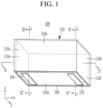
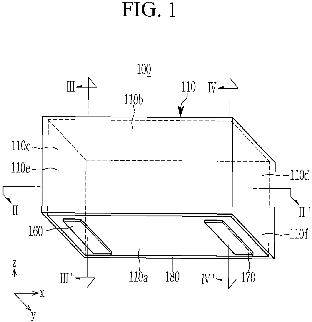
- FIG. 1 is a perspective view illustrating an external shape of an electronic component according to an embodiment
- FIG. 2 is a cross-sectional view of the electronic component taken along line II-II' in FIG. 1
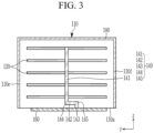
- FIG. 3 is a cross-sectional view of the electronic component taken along line III-III' in FIG. 1
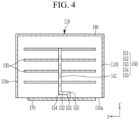
- FIG. 4 is a cross-sectional view of the electronic component taken along line IV-IV' in FIG. 1 .
- an electronic component 100 is a multilayer ceramic capacitor, and specifically includes a capacitor body 110, a first connection electrode 140, a second connection electrode 150, a first external electrode 160, and a second external electrode 170.
- the capacitor body 110 may include a plurality of dielectric layers 112, and a plurality of internal electrodes 120 and 130 disposed in the stacking direction (z-axis direction in the drawings) and spaced apart from one another with one dielectric layer 112 interposed therebetween.
- the plurality of internal electrodes 120 and 130 may include first and second internal electrodes 120 and 130 alternately positioned in the stacking direction.
- the capacitor body 110 may have an approximately hexahedral shape and include first and second surfaces 110a and 110b facing each other in the stacking direction, third and fourth surfaces 110c and 110d facing each other in a first direction (x-axis direction in the drawings), and fifth and sixth surfaces 110e and 110f facing each other in a second direction (y-axis direction in the drawings).
- the first surface 110a and the second surface 110b may be respectively a lower surface and an upper surface of the capacitor body 110.
- the third surface 110c and the fourth surface 110d may be respectively a left surface and a right surface of the capacitor body 110.
- the fifth surface 110e and the sixth surface 110f may be respectively a front surface and a rear surface of the capacitor body 110.
- FIG. 5 is an exploded perspective view of a capacitor body of the electronic component illustrated in FIG. 1 .
- the plurality of dielectric layers 112 may be disposed in the stacking direction, any one of the first internal electrode 120 and the second internal electrode 130 is positioned on each of the dielectric layers 112.
- the first internal electrode 120 and the second internal electrode 130 may be alternately positioned one by one in the stacking direction and each have a smaller area than the dielectric layer 112.
- the dielectric layer 112 may include a ceramic material having high permittivity.
- the ceramic material may include dielectric ceramic containing substances such as BaTiOs, CaTiOs, SrTiOs, or GaZrOs .
- the ceramic material may further include auxiliary substances such as a Mn compound, a Fe compound, a Cr compound, a Co compound, and a Ni compound in addition to the above-mentioned substances.
- the ceramic material may be (Ba 1-x Ca x )TiO 3 , Ba(Ti 1-y Ca y )O 3 , (Ba 1-x Ca x )(Ti 1-y Zr y )O 3 , Ba(Ti 1-y Zr y )O 3 , or the like made by partially applying Ca, Zr, or the like to BaTiO 3 -based dielectric ceramic.
- the first and second internal electrodes 120 and 130 may be manufactured by printing conductive paste containing metal onto the dielectric layer 112.
- the first and second internal electrodes 120 and 130 may each include Ni, Cu, Pd, and Ag as main substances.
- One side (left) edge of the first internal electrode 120 may overlap, in the stacking direction, one side (left) edge of two opposite side edges of the dielectric layer 112 based on the first direction.
- the other side (right) edge of the second internal electrode 130 may overlap, in the stacking direction, the other side (right) edge of the two opposite side edges of the dielectric layer 112 based on the first direction.
- the dielectric layers 112 may be additionally disposed at two opposite ends (an uppermost end and a lowermost end) based on the stacking direction.
- the capacitor body 110 may be manufactured by disposing the plurality of dielectric layers 112 and the first and second internal electrodes 120 and 130 in the above-mentioned way and then performing a sintering process.
- the plurality of dielectric layers 112 may be integrated to the extent that boundaries therebetween cannot be identified.
- an edge of the first internal electrode 120 may be exposed from the third surface 110c of the capacitor body 110, and an edge of the second internal electrode 130 may be exposed from the fourth surface 110d of the capacitor body 110.
- the capacitor body 110 may at least include an insulation layer 180 positioned on the third surface 110c and the fourth surface 110d.
- the insulation layer 180 may at least cover the third surface 110c and the fourth surface 110d to prevent the edges of the first and second internal electrodes 120 and 130 from being exposed from the outside of the capacitor body 110.
- the insulation layer 180 may be positioned on the remaining surfaces of the capacitor body 110, except for the first surface 110a, i.e., positioned on the second to sixth surfaces 110b, 110c, 110d, 110e, and 110f.
- the insulation layer 180 may be manufactured by coating the second to sixth surfaces 110b, 110c, 110d, 110e, and 110f of the capacitor body 110 with insulating resin and then performing a drying process.
- the insulation layer 180 serves to improve durability and reliability of the capacitor body 110.
- the first connection electrode 140 is connected to the plurality of first internal electrodes 120 in the capacitor body 110, and the second connection electrode 150 is connected to the plurality of second internal electrodes 130 in the capacitor body 110.
- the first connection electrode 140 and the second connection electrode 150 are positioned at a distance therebetween in the first direction. The ends of the first and second connection electrodes 140 and 150 may be exposed from the first surface 110a of the capacitor body 110.
- the first connection electrode 140 may include a main junction portion 141 extending in the stacking direction and configured to penetrate the plurality of first internal electrodes 120, and a bypass portion 142 connected to the main junction portion 141 and extending in a planar direction in the dielectric layer 112.
- the bypass portion 142 may extend in a direction substantially crossing the stacking direction.
- the direction substantially crossing the stacking direction may form an angle of more than 0° and 90° or less with the stacking direction.
- the second connection electrode 150 may include a main junction portion 151 extending in the stacking direction and configured to penetrate the plurality of second internal electrodes 130, and a bypass portion 152 connected to the main junction portion 151 and extending in the planar direction in the dielectric layer 112.
- the main junction portion 141 of the first connection electrode 140 may be positioned to be close to the third surface 110c of the capacitor body 110 so as not to adjoin the second internal electrode 130. That is, the main junction portion 141 of the first connection electrode 140 may be positioned at a distance from the edge of the second internal electrode 130 in the first direction and positioned between the third surface 110c of the capacitor body 110 and the edge of the second internal electrode 130.
- the main junction portion 151 of the second connection electrode 150 may be positioned to be close to the fourth surface 110d of the capacitor body 110 so as not to adjoin the first internal electrode 120. That is, the main junction portion 151 of the second connection electrode 150 may be positioned at a distance from the edge of the first internal electrode 120 in the first direction and positioned between the fourth surface 110d of the capacitor body 110 and the edge of the first internal electrode 120.
- the main junction portion 141 of the first connection electrode 140 may penetrate the plurality of first internal electrodes 120 and the plurality of dielectric layers 112 in the stacking direction and be in contact with and electrically connected to the plurality of first internal electrodes 120.
- the main junction portion 151 of the second connection electrode 150 may penetrate the plurality of second internal electrodes 130 and the plurality of dielectric layers 112 in the stacking direction and be in contact with and electrically connected to the plurality of second internal electrodes 130.
- each of the main junction portions 141 and 151 may be positioned at a distance from the first surface 110a of the capacitor body 110. Specifically, one end (lower end) of each of the main junction portions 141 and 151 may be positioned in a lowermost end dielectric layer (indicated by'112a' in FIG. 2 , for convenience) which adjoins the first surface 110a among the plurality of dielectric layers 112 that constitute the capacitor body 110.
- the lowermost end dielectric layer 112a may be a dielectric layer, which is positioned between a lowermost end internal electrode and the first surface 110a among the plurality of internal electrodes 120 and 130, and have a larger thickness than the dielectric layer 112 positioned between the first internal electrode 120 and the second internal electrode 130.
- the thickness of each of the dielectric layers may be measured by, for example, scanning electron microscopy. Other methods and/or tools appreciated by one of ordinary skill in the art, even if not described in the present disclosure, may also be used.
- the bypass portions 142 and 152 may each be connected to one end (lower end) of each of the main junction portions 141 and 151 in the lowermost end dielectric layer 112a and positioned to extend in the planar direction.
- the bypass portions 142 and 152 may extend in the second direction (y-axis direction in the drawings) of the planar direction.
- bypass portions 142 and 152 extend in the first direction (x-axis direction in the drawings) of the planar direction, a distance between the bypass portions 142 and 152 of the first and second connection electrodes 140 and 150 may become closer, and a distance between the first and second external electrodes 160 and 170 to be described below may become closer. In this case, interference may occur between the first connection electrode 140 and the second connection electrode 150.
- the bypass portions 142 and 152 may extend in the second direction of the planar direction and prevent the interference between the first and second connection electrodes 140 and 150.
- the main junction portions 141 and 151 extend in the stacking direction, and the bypass portions 142 and 152 extend in the second direction, such that the first bent portions 144 and 154 are present between the main junction portions 141 and 151 and the bypass portions 142 and 152.
- the first bent portions 144 and 154 may each have various shapes such as a shape bent at a right angle or a shape bent roundly while having a predetermined curvature.
- FIGS. 3 and 4 illustrates the first example.
- the shapes of the first bent portions 144 and 154 are not limited to the illustrated examples.
- the first and second connection electrodes 140 and 150 may include conductive portions 143 and 153 connected to ends of the bypass portions 142 and 152.
- the conductive portions 143 and 153 may extend in the stacking direction in the lowermost end dielectric layer 112a and be exposed from the first surface 110a of the capacitor body 110. That is, the ends of the conductive portions 143 and 153 may be the ends of the first and second connection electrodes 140 and 150.
- the bypass portions 142 and 152 extend in the second direction, and the conductive portions 143 and 153 extend in the stacking direction, such that second bent portions 145 and 155 are present between the bypass portions 142 and 152 and the conductive portions 143 and 153.
- the second bent portions 145 and 155 may each have various shapes such as a shape bent at a right angle or a shape bent roundly while having a predetermined curvature.
- FIGS. 3 and 4 illustrates the first example.
- the shapes of the second bent portions 145 and 155 are not limited to the illustrated examples.
- the first and second connection electrodes 140 and 150 are connected to the plurality of internal electrodes 120 and 130 by means of the main junction portions 141 and 151.
- the main junction portions 141 and 151 may be connected to the bypass portions 142 and 152 and the conductive portions 143 and 153 without being exposed directly from the first surface 110a of the capacitor body 110.
- the first and second connection electrodes 140 and 150 may each have lengths extended by the bypass portions 142 and 152 and the conductive portions 143 and 153 and each have the two bent portions 144, 145, 154, and 155 in the capacitor body 110.
- the first external electrode 160 and the second external electrode 170 may be positioned on the first surface 110a of the capacitor body 110 and positioned at a distance therebetween in the first direction.
- the first external electrode 160 may be connected to the first connection electrode 140 by coming into contact with the end of the first connection electrode 140
- the second external electrode 170 may be connected to the second connection electrode 150 by coming into contact with the end of the second connection electrode 150.
- the first and second external electrodes 160 and 170 may be mounted on a circuit board (not illustrated) of an electronic product and electrically connect the plurality of internal electrodes 120 and 130 and the circuit board.
- the first and second connection electrodes 140 and 150 may be manufactured by forming through-holes in the capacitor body 110, filling the through-holes with conductive materials, and performing a sintering process.
- the first and second connection electrodes 140 and 150 may be manufactured by forming through-holes in the capacitor body 110 by using a laser or the like, filling the through-holes with conductive materials containing metal, and then performing a sintering process.
- fine gaps may be formed around the first and second connection electrodes 140 and 150 because of a difference in contraction percentage between the constituent materials of the capacitor body 110 and the constituent materials of the first and second connection electrodes 140 and 150. Degrees to which the gaps are formed may be different in the main junction portions 141 and 151 and the bypass portions 142 and 152.
- the main junction portions 141 and 151, the dielectric layer 112, and the internal electrodes 120 and 130 are alternately in contact with one another in the stacking direction.
- the three types of constituent elements including the main junction portions 141 and 151, the dielectric layer 112, and the internal electrodes 120 and 130 may mechanically interact with one another to produce various changes in contraction percentage.
- the bypass portions 142 and 152 and the conductive portions 143 and 153 are in contact with the single material, i.e., the dielectric layer 112. Therefore, the occurrence of gaps may be further suppressed in the bypass portions 142 and 152 and the conductive portions 143 and 153 than in the main junction portions 141 and 151.
- the bypass portions 142 and 152 and the conductive portions 143 and 153 may implement very close contact surfaces with the dielectric layer 112.
- the electronic component 100 may improve moisture resistance reliability by effectively blocking the penetration of moisture into the main junction portions 141 and 151.
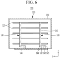
- FIGS. 6 and 7 are cross-sectional views illustrating an interior of an electronic component according to another embodiment.
- an electronic component 200 may include the same basic configuration as the electronic component 100 according to the embodiment described with reference to FIGS. 1 to 4 , except that the first connection electrode 140 is provided as a plurality of first connection electrodes 140, and the second connection electrode 150 is provided as a plurality of second connection electrodes 150.
- the plurality of first connection electrodes 140 may be positioned between the third surface 110c (see FIG. 1 ) of the capacitor body 110 and the plurality of second internal electrodes 130 and positioned at distances therebetween in the second direction.
- the plurality of second connection electrodes 150 may be positioned between the fourth surface 110d (see FIG. 1 ) of the capacitor body 110 and the plurality of first internal electrodes 120 and positioned at distances therebetween in the second direction.
- the plurality of first connection electrodes 140 may be connected to the first external electrode 160, and the plurality of second connection electrodes 150 may be connected to the second external electrode 170.
- FIGS. 6 and 7 illustrate that two first connection electrodes 140 and two second connection electrodes 150 are disposed. However, the number of first and second connection electrodes 140 and 150 is not limited to the illustrated example.
- first connection electrode 140 or any one of the second connection electrodes 150 may serve to connect the plurality of internal electrodes 120 and 130, thereby implementing an effect of reducing a risk caused by the disconnection.
- the electronic component of Example 1 is the electronic component according to the embodiment described with reference to FIGS. 1 to 4
- the electronic component of Example 2 is the electronic component according to the embodiment described with reference to FIGS. 6 and 7 in which the two first connection electrodes and the two second connection electrodes are provided.
- the electronic component of Example 2 includes the same basic configuration as the electronic component of Example 1, except for the number of first and second connection electrodes.
- the electronic component of the Comparative Example includes the same basic configuration as the electronic component of Example 1, except that the first and second connection electrodes are straight shapes parallel to the stacking direction.
- Example 1 Forty electronic components of each of Example 1, Example 2, and Comparative Example were prepared and mounted on circuit boards. Then, moisture resistance reliability was measured by using ESPEC (PR-3J) equipment under a condition of 85°C, relative humidity (R.H.) of 85%, 2Vr (twice a rated voltage), and 300 hours. The results are shown in Table 1 below. (Table 1) Defect rate(%) Comparative Example 47.5 Example 1 0 Example 2 0
Landscapes
- Engineering & Computer Science (AREA)
- Power Engineering (AREA)
- Microelectronics & Electronic Packaging (AREA)
- Manufacturing & Machinery (AREA)
- Chemical & Material Sciences (AREA)
- Ceramic Engineering (AREA)
- Inorganic Chemistry (AREA)
- Fixed Capacitors And Capacitor Manufacturing Machines (AREA)
- Ceramic Capacitors (AREA)
Abstract
Description
- The present disclosure relates to an electronic component, and more particularly, to a multilayer ceramic capacitor.
- A multilayer ceramic capacitor (MLCC) refers to a chip-shaped condenser mounted on a circuit board of various types of electronic products and configured to be charged with electricity or discharged. The multilayer ceramic capacitor has a structure in which internal electrodes having opposite polarities are alternately stacked one by one with dielectric layers (ceramic layers) interposed therebetween.
- Recently, with the trend of manufacturing electronic products having high performance and multiple functions, the use of multilayer ceramic capacitors has increased. With the progress of miniaturization and integration of electronic components, there is a consistently increasing need for multilayer ceramic capacitors having small scales and high capacities. However, a technology for increasing the number of stacked internal electrodes or thinning a dielectric layer, which is a representative method capable of increasing capacitance, gradually approaches a technical limitation, which slows down the improvement.
- Therefore, in order to increase capacitance in other aspects, there has been proposed a method of decreasing volumes of elements irrelevant to the implementation of capacity among constituent elements of the multilayer ceramic capacitor and increasing volumes of parts that contribute to the increase in capacity to the extent of the decreased volumes. For example, a representative method provides a configuration in which a connection electrode penetrates a dielectric layer and a plurality of internal electrodes.
- The connection electrode may be manufactured by a process of forming through-holes in the dielectric layer and the plurality of internal electrodes, filling the through-holes with conductive materials, and then performing a sintering process. However, in this case, gaps may be formed between the connection electrode and the through-holes because of a difference in sintering contraction percentage between the dielectric layer, the internal electrode, and the conductive material, and outside moisture may penetrate through the gaps, which degrades moisture resistance reliability.
- The present disclosure has been made in an effort to provide an electronic component capable of improving moisture resistance reliability by preventing outside moisture from penetrating into the electronic component through a connection electrode in a configuration in which the connection electrode is used to electrically connect a plurality of internal electrodes.
- However, the object to be achieved by the embodiments of the present disclosure is not limited to the above-mentioned object but may be variously expanded without departing from the technical spirit of the present disclosure.
- An electronic component according to an embodiment includes a capacitor body, a connection electrode, and an external electrode. The capacitor body includes a dielectric layer, a plurality of internal electrodes disposed in a stacking direction and spaced apart from one another with the dielectric layer interposed therebetween, and first and second surfaces facing each other in the stacking direction. The connection electrode includes a main junction portion extending in the stacking direction and configured to penetrate the plurality of internal electrodes, a bypass portion connected to the main junction portion and extending in a planar direction in the dielectric layer, and an end extending from the first surface. The connection electrode is connected to the plurality of internal electrodes in the capacitor body. The external electrode is positioned on the first surface and connected to the connection electrode.
- The capacitor body may include a lowermost end dielectric layer configured to adjoin the first surface, and the bypass portion may be positioned in the lowermost end dielectric layer.
- The lowermost end dielectric layer may have a larger thickness than the dielectric layer positioned between the plurality of internal electrodes.
- The connection electrode may further include a conductive portion connected to the bypass portion. The conductive portion may extend in the stacking direction in the lowermost end dielectric layer, may extend to the first surface, and may be in contact with the external electrode.
- The planar direction may include first and second directions orthogonal to each other, and the capacitor body may include third and fourth surfaces facing each other in the first direction. The plurality of internal electrodes may include a plurality of first internal electrodes and a plurality of second internal electrodes alternately positioned one by one in the stacking direction. Edges of the plurality of first internal electrodes may be extended from the third surface, and edges of the plurality of second internal electrodes may be extended from the fourth surface.
- The bypass portion may be positioned to extend in the second direction.
- The plurality of first internal electrodes may be positioned at a distance from the fourth surface, and the plurality of second internal electrodes may be positioned at a distance from the third surface. The connection electrode may include: a first connection electrode connected to the plurality of first internal electrodes, the first connection electrode may include a first main junction portion positioned between the third surface and the plurality of second internal electrodes; and a second connection electrode connected to the plurality of second internal electrodes, the second connection electrode may include a second main junction portion positioned between the fourth surface and the plurality of first internal electrodes.
- The first connection electrode may include a plurality of first connection electrodes, and the second connection electrode may include a plurality of second connection electrodes. The plurality of first connection electrodes may be spaced apart from each other in the second direction, and the plurality of second connection electrodes may be spaced apart from each other in the second direction.
- The capacitor body may further include an insulation layer configured to cover the third surface and the fourth surface.
- An electronic component according to another embodiment includes a capacitor body, a connection electrode, and an external electrode. The capacitor body includes a dielectric layer, a plurality of internal electrodes disposed in a stacking direction and spaced apart from one another with the dielectric layer interposed therebetween, and first and second surfaces facing each other in the stacking direction. The connection electrode is configured to penetrate the plurality of internal electrodes and connected to the plurality of internal electrodes, and the connection electrode has at least one bent portion in the capacitor body and an end extending from the first surface. The external electrode is positioned on the first surface and connected to the connection electrode.
- The at least one bent portion may include a first bent portion. The connection electrode may further include a main junction portion extending in the stacking direction and configured to penetrate the plurality of internal electrodes, and a bypass portion connected to the main junction portion by means the first bent portion and extending in a planar direction in the dielectric layer. The first bent portion may have any one of a shape bent at a right angle and a shape roundly bent.
- The at least one bent portion may further include a first bent portion. The connection electrode may further include a conductive portion connected to the bypass portion by the second bent portion. The conductive portion may extend in the stacking direction in the dielectric layer, may extend to the first surface, and may be in contact with the external electrode. The second bent portion may have any one of a shape bent at a right angle and a shape roundly bent.
- The capacitor body may further include a lowermost end dielectric layer configured to adjoin the first surface, and the bypass portion and the conductive portion may be positioned in the lowermost end dielectric layer.
- The lowermost end dielectric layer may have a larger thickness than the dielectric layer positioned between the plurality of internal electrodes.
- The connection electrode may include a plurality of connection electrodes spaced apart from each other.
- An electronic component according to an embodiment includes a capacitor body, a connection electrode, and an external electrode. The capacitor body includes a dielectric layer, a plurality of internal electrodes disposed in a stacking direction and spaced apart from one another with the dielectric layer interposed therebetween, and first and second surfaces facing each other in the stacking direction. The connection electrode includes a main junction portion extending in the stacking direction and configured to penetrate the plurality of internal electrodes, a bypass portion connected to the main junction portion and extending in a direction substantially crossing the stacking direction, and an end extending from the first surface. The connection electrode is connected to the plurality of internal electrodes in the capacitor body. The external electrode is positioned on the first surface and connected to the connection electrode.
- The connection electrode may further include a conductive portion connected to the bypass portion. In a cross-section of the electronic component in the stacking direction and a direction orthogonal to the stacking direction, a central axis of the main junction portion along the stacking direction may be offset from a central axis of the conductive portion along the stacking direction.
- In a cross-section of the electronic component in the stacking direction and a direction orthogonal to the stacking direction, the main junction portion and the conductive portion may not overlap each other along the stacking direction.
- The main junction portion may penetrate through at least one internal electrode among the plurality of internal electrodes.
- In the electronic component according to the embodiment, the penetration of moisture is blocked by the bypass route in the capacitor body even though the moisture is intended to penetrate into the connection electrode from the outside. Therefore, the electronic component according to the embodiment may improve the moisture resistance reliability by effectively blocking the penetration of moisture into the main junction portion.
-
-
FIG. 1 is a perspective view illustrating an external shape of an electronic component according to an embodiment. -
FIG. 2 is a cross-sectional view of the electronic component taken along line II-II' inFIG. 1 . -
FIG. 3 is a cross-sectional view of the electronic component taken along line III-III' inFIG. 1 . -
FIG. 4 is a cross-sectional view of the electronic component taken along line IV-IV' inFIG. 1 . -
FIG. 5 is an exploded perspective view of a capacitor body of the electronic component illustrated inFIG. 1 . -
FIGS. 6 and7 are cross-sectional views illustrating an interior of an electronic component according to another embodiment. - Hereinafter, embodiments of the present disclosure will be described in detail with reference to the accompanying drawings so that those with ordinary skill in the art to which the present disclosure pertains may easily carry out the embodiments. In the drawings, a part irrelevant to the description will be omitted to clearly describe the present disclosure, and the same or similar constituent elements will be designated by the same reference numerals throughout the specification. Some constituent elements in the accompanying drawings are illustrated in an exaggerated or schematic form or are omitted. A size of each constituent element does not entirely reflect an actual size.
- In addition, it should be interpreted that the accompanying drawings are provided only to allow those skilled in the art to easily understand the embodiments disclosed in the present specification, and the technical spirit disclosed in the present specification is not limited by the accompanying drawings, and includes all alterations, equivalents, and alternatives that are included in the spirit and the technical scope of the present disclosure.
- The terms including ordinal numbers such as "first," "second," and the like may be used to describe various constituent elements, but the constituent elements are not limited by the terms. These terms are used only to distinguish one constituent element from another constituent element.
- In addition, when one component such as a layer, a film, a region, or a plate is described as being positioned "above" or "on" another component, one component can be positioned "directly on" another component, and one component can also be positioned on another component with other components interposed therebetween. On the contrary, when one component is described as being positioned "directly above" another component, there is no component therebetween. In addition, when a component is described as being positioned "above" or "on" a reference part, the component may be positioned "above" or "below" the reference part, and this configuration does not necessarily mean that the component is positioned "above" or "on" the reference part in a direction opposite to gravity.
- Throughout the specification, the terms "comprises," "comprising," "includes," "including," "containing," "has," "having" or other variations thereof are inclusive and therefore specify the presence of stated features, integers, steps, operations, elements, components, and/or combinations thereof, but do not preclude the presence or addition of one or more other features, integers, steps, operations, elements, components, and/or combinations thereof. Therefore, unless explicitly described to the contrary, the word "comprise/include" and variations such as "comprises/includes" or "comprising/including" will be understood to imply the inclusion of stated elements, not the exclusion of any other elements.
- Throughout the specification, the word "in a plan view" means when an object is viewed from above, and the word "in a cross-sectional view" means when a cross section made by vertically cutting an object is viewed from a lateral side.
- Throughout the specification, when one constituent element is referred to as being "connected to" another constituent element, one constituent element can be "directly connected to" the other constituent element, and one constituent element can also be "indirectly connected to," "physically connected to," or "electrically connected to" the other element with other elements therebetween. Further, the constituent elements are defined as different names according to positions or functions thereof, but the constituent elements may be integrated.
- In the present specification, in describing the electronic component, a direction in which main components of the electronic component are stacked is defined as a 'stacking direction' that may be a 'thickness direction'. In addition, a direction parallel to a plane perpendicular to the stacking direction may be defined as a 'planar direction', and the planar direction may include a 'first direction' and a 'second direction' that are orthogonal to each other.
-
FIG. 1 is a perspective view illustrating an external shape of an electronic component according to an embodiment, andFIG. 2 is a cross-sectional view of the electronic component taken along line II-II' inFIG. 1 .FIG. 3 is a cross-sectional view of the electronic component taken along line III-III' inFIG. 1 , andFIG. 4 is a cross-sectional view of the electronic component taken along line IV-IV' inFIG. 1 . - With reference to
FIGS. 1 to 4 , anelectronic component 100 according to an embodiment is a multilayer ceramic capacitor, and specifically includes acapacitor body 110, afirst connection electrode 140, asecond connection electrode 150, a firstexternal electrode 160, and a secondexternal electrode 170. - The
capacitor body 110 may include a plurality ofdielectric layers 112, and a plurality ofinternal electrodes dielectric layer 112 interposed therebetween. The plurality ofinternal electrodes internal electrodes - The
capacitor body 110 may have an approximately hexahedral shape and include first andsecond surfaces fourth surfaces sixth surfaces first surface 110a and thesecond surface 110b may be respectively a lower surface and an upper surface of thecapacitor body 110. Thethird surface 110c and thefourth surface 110d may be respectively a left surface and a right surface of thecapacitor body 110. Thefifth surface 110e and thesixth surface 110f may be respectively a front surface and a rear surface of thecapacitor body 110. -
FIG. 5 is an exploded perspective view of a capacitor body of the electronic component illustrated inFIG. 1 . - With reference to
FIG. 5 , the plurality ofdielectric layers 112 may be disposed in the stacking direction, any one of the firstinternal electrode 120 and the secondinternal electrode 130 is positioned on each of the dielectric layers 112. The firstinternal electrode 120 and the secondinternal electrode 130 may be alternately positioned one by one in the stacking direction and each have a smaller area than thedielectric layer 112. - The
dielectric layer 112 may include a ceramic material having high permittivity. For example, the ceramic material may include dielectric ceramic containing substances such as BaTiOs, CaTiOs, SrTiOs, or GaZrOs . In addition, the ceramic material may further include auxiliary substances such as a Mn compound, a Fe compound, a Cr compound, a Co compound, and a Ni compound in addition to the above-mentioned substances. For example, the ceramic material may be (Ba1-xCax)TiO3, Ba(Ti1-yCay)O3, (Ba1-xCax)(Ti1-yZry)O3, Ba(Ti1-yZry)O3, or the like made by partially applying Ca, Zr, or the like to BaTiO3-based dielectric ceramic. - The first and second
internal electrodes dielectric layer 112. The first and secondinternal electrodes - One side (left) edge of the first
internal electrode 120 may overlap, in the stacking direction, one side (left) edge of two opposite side edges of thedielectric layer 112 based on the first direction. The other side (right) edge of the secondinternal electrode 130 may overlap, in the stacking direction, the other side (right) edge of the two opposite side edges of thedielectric layer 112 based on the first direction. As necessary, thedielectric layers 112 may be additionally disposed at two opposite ends (an uppermost end and a lowermost end) based on the stacking direction. - The
capacitor body 110 may be manufactured by disposing the plurality ofdielectric layers 112 and the first and secondinternal electrodes capacitor body 110 that has been subjected to the sintering process, the plurality ofdielectric layers 112 may be integrated to the extent that boundaries therebetween cannot be identified. - With reference back to
FIGS. 1 to 4 , an edge of the firstinternal electrode 120 may be exposed from thethird surface 110c of thecapacitor body 110, and an edge of the secondinternal electrode 130 may be exposed from thefourth surface 110d of thecapacitor body 110. Thecapacitor body 110 may at least include aninsulation layer 180 positioned on thethird surface 110c and thefourth surface 110d. Theinsulation layer 180 may at least cover thethird surface 110c and thefourth surface 110d to prevent the edges of the first and secondinternal electrodes capacitor body 110. - The
insulation layer 180 may be positioned on the remaining surfaces of thecapacitor body 110, except for thefirst surface 110a, i.e., positioned on the second tosixth surfaces insulation layer 180 may be manufactured by coating the second tosixth surfaces capacitor body 110 with insulating resin and then performing a drying process. Theinsulation layer 180 serves to improve durability and reliability of thecapacitor body 110. - The
first connection electrode 140 is connected to the plurality of firstinternal electrodes 120 in thecapacitor body 110, and thesecond connection electrode 150 is connected to the plurality of secondinternal electrodes 130 in thecapacitor body 110. Thefirst connection electrode 140 and thesecond connection electrode 150 are positioned at a distance therebetween in the first direction. The ends of the first andsecond connection electrodes first surface 110a of thecapacitor body 110. - The
first connection electrode 140 may include amain junction portion 141 extending in the stacking direction and configured to penetrate the plurality of firstinternal electrodes 120, and abypass portion 142 connected to themain junction portion 141 and extending in a planar direction in thedielectric layer 112. In some embodiments of the application, thebypass portion 142 may extend in a direction substantially crossing the stacking direction. For example, the direction substantially crossing the stacking direction may form an angle of more than 0° and 90° or less with the stacking direction. Thesecond connection electrode 150 may include amain junction portion 151 extending in the stacking direction and configured to penetrate the plurality of secondinternal electrodes 130, and abypass portion 152 connected to themain junction portion 151 and extending in the planar direction in thedielectric layer 112. - The
main junction portion 141 of thefirst connection electrode 140 may be positioned to be close to thethird surface 110c of thecapacitor body 110 so as not to adjoin the secondinternal electrode 130. That is, themain junction portion 141 of thefirst connection electrode 140 may be positioned at a distance from the edge of the secondinternal electrode 130 in the first direction and positioned between thethird surface 110c of thecapacitor body 110 and the edge of the secondinternal electrode 130. - The
main junction portion 151 of thesecond connection electrode 150 may be positioned to be close to thefourth surface 110d of thecapacitor body 110 so as not to adjoin the firstinternal electrode 120. That is, themain junction portion 151 of thesecond connection electrode 150 may be positioned at a distance from the edge of the firstinternal electrode 120 in the first direction and positioned between thefourth surface 110d of thecapacitor body 110 and the edge of the firstinternal electrode 120. - The
main junction portion 141 of thefirst connection electrode 140 may penetrate the plurality of firstinternal electrodes 120 and the plurality ofdielectric layers 112 in the stacking direction and be in contact with and electrically connected to the plurality of firstinternal electrodes 120. Themain junction portion 151 of thesecond connection electrode 150 may penetrate the plurality of secondinternal electrodes 130 and the plurality ofdielectric layers 112 in the stacking direction and be in contact with and electrically connected to the plurality of secondinternal electrodes 130. - One end (lower end) of each of the
main junction portions first surface 110a of thecapacitor body 110. Specifically, one end (lower end) of each of themain junction portions FIG. 2 , for convenience) which adjoins thefirst surface 110a among the plurality ofdielectric layers 112 that constitute thecapacitor body 110. The lowermostend dielectric layer 112a may be a dielectric layer, which is positioned between a lowermost end internal electrode and thefirst surface 110a among the plurality ofinternal electrodes dielectric layer 112 positioned between the firstinternal electrode 120 and the secondinternal electrode 130. The thickness of each of the dielectric layers may be measured by, for example, scanning electron microscopy. Other methods and/or tools appreciated by one of ordinary skill in the art, even if not described in the present disclosure, may also be used. - The
bypass portions main junction portions end dielectric layer 112a and positioned to extend in the planar direction. Thebypass portions - Assuming that the
bypass portions bypass portions second connection electrodes external electrodes first connection electrode 140 and thesecond connection electrode 150. Thebypass portions second connection electrodes - The
main junction portions bypass portions bent portions main junction portions bypass portions bent portions FIGS. 3 and4 illustrates the first example. However, the shapes of the firstbent portions - The first and
second connection electrodes conductive portions bypass portions conductive portions end dielectric layer 112a and be exposed from thefirst surface 110a of thecapacitor body 110. That is, the ends of theconductive portions second connection electrodes - The
bypass portions conductive portions bent portions bypass portions conductive portions bent portions FIGS. 3 and4 illustrates the first example. However, the shapes of the secondbent portions - As described above, the first and
second connection electrodes internal electrodes main junction portions main junction portions bypass portions conductive portions first surface 110a of thecapacitor body 110. In thecapacitor body 110, the first andsecond connection electrodes bypass portions conductive portions bent portions capacitor body 110. - The first
external electrode 160 and the secondexternal electrode 170 may be positioned on thefirst surface 110a of thecapacitor body 110 and positioned at a distance therebetween in the first direction. The firstexternal electrode 160 may be connected to thefirst connection electrode 140 by coming into contact with the end of thefirst connection electrode 140, and the secondexternal electrode 170 may be connected to thesecond connection electrode 150 by coming into contact with the end of thesecond connection electrode 150. The first and secondexternal electrodes internal electrodes - The first and
second connection electrodes capacitor body 110, filling the through-holes with conductive materials, and performing a sintering process. For example, the first andsecond connection electrodes capacitor body 110 by using a laser or the like, filling the through-holes with conductive materials containing metal, and then performing a sintering process. - Meanwhile, during the sintering process, fine gaps may be formed around the first and
second connection electrodes capacitor body 110 and the constituent materials of the first andsecond connection electrodes main junction portions bypass portions - Specifically, the
main junction portions dielectric layer 112, and theinternal electrodes main junction portions dielectric layer 112, and theinternal electrodes bypass portions conductive portions dielectric layer 112. Therefore, the occurrence of gaps may be further suppressed in thebypass portions conductive portions main junction portions bypass portions conductive portions dielectric layer 112. - As a result, even though moisture is intended to penetrate into the
main junction portions electronic component 100, the penetration of moisture is blocked by bypass routes including theconductive portions bypass portions electronic component 100 according to the embodiment may improve moisture resistance reliability by effectively blocking the penetration of moisture into themain junction portions -
FIGS. 6 and7 are cross-sectional views illustrating an interior of an electronic component according to another embodiment. - With reference to
FIGS. 6 and7 , anelectronic component 200 according to the present embodiment may include the same basic configuration as theelectronic component 100 according to the embodiment described with reference toFIGS. 1 to 4 , except that thefirst connection electrode 140 is provided as a plurality offirst connection electrodes 140, and thesecond connection electrode 150 is provided as a plurality ofsecond connection electrodes 150. - The plurality of
first connection electrodes 140 may be positioned between thethird surface 110c (seeFIG. 1 ) of thecapacitor body 110 and the plurality of secondinternal electrodes 130 and positioned at distances therebetween in the second direction. The plurality ofsecond connection electrodes 150 may be positioned between thefourth surface 110d (seeFIG. 1 ) of thecapacitor body 110 and the plurality of firstinternal electrodes 120 and positioned at distances therebetween in the second direction. - The plurality of
first connection electrodes 140 may be connected to the firstexternal electrode 160, and the plurality ofsecond connection electrodes 150 may be connected to the secondexternal electrode 170.FIGS. 6 and7 illustrate that twofirst connection electrodes 140 and twosecond connection electrodes 150 are disposed. However, the number of first andsecond connection electrodes - In the
electronic component 200 of the present embodiment, even though any one of thefirst connection electrodes 140 or any one of thesecond connection electrodes 150 is disconnected in thecapacitor body 110, anotherfirst connection electrode 140 or anothersecond connection electrode 150 may serve to connect the plurality ofinternal electrodes - Next, experiments for evaluating moisture resistance reliability on electronic components according to Example 1, Example 2, and Comparative Example will be described.
- The electronic component of Example 1 is the electronic component according to the embodiment described with reference to
FIGS. 1 to 4 , and the electronic component of Example 2 is the electronic component according to the embodiment described with reference toFIGS. 6 and7 in which the two first connection electrodes and the two second connection electrodes are provided. The electronic component of Example 2 includes the same basic configuration as the electronic component of Example 1, except for the number of first and second connection electrodes. The electronic component of the Comparative Example includes the same basic configuration as the electronic component of Example 1, except that the first and second connection electrodes are straight shapes parallel to the stacking direction. - Forty electronic components of each of Example 1, Example 2, and Comparative Example were prepared and mounted on circuit boards. Then, moisture resistance reliability was measured by using ESPEC (PR-3J) equipment under a condition of 85°C, relative humidity (R.H.) of 85%, 2Vr (twice a rated voltage), and 300 hours. The results are shown in Table 1 below.
(Table 1) Defect rate(%) Comparative Example 47.5 Example 1 0 Example 2 0 - It can be seen that in the case of the electronic component of Comparative Example in which the first and second connection electrodes are straight shapes, an insulation resistance defect occurs on half of the electronic component because of penetration of moisture. In contrast, no insulation resistance defect caused by penetration of moisture occurs on the electronic component of Examples 1 and 2. The electronic components of Examples 1 and 2 may provide the bypass routes on the connection electrode, thereby preventing the insulation resistance defect caused by the penetration of moisture.
- While the embodiments of the present disclosure have been described above, the present disclosure is not limited thereto, and various modifications can be made and carried out within the scope of the claims, the detailed description of the disclosure, and the accompanying drawings, and also fall within the scope of the present disclosure.
- The following is a list of further preferred embodiments of the invention:
- Embodiment 1: An electronic component comprising:
- a capacitor body comprising:
a dielectric layer; - a plurality of internal electrodes disposed in a stacking direction and spaced apart from one another with the dielectric layer interposed therebetween; and
first and second surfaces facing each other in the stacking direction; - a connection electrode comprising:
- a main junction portion extending in the stacking direction and configured to penetrate the plurality of internal electrodes;
- a bypass portion connected to the main junction portion and extending in a planar direction in the dielectric layer; and
- an end extending from the first surface, wherein the connection electrode is connected to the plurality of internal electrodes in the capacitor body ; and
- an external electrode positioned on the first surface and connected to the connection electrode.
- a capacitor body comprising:
- Embodiment 2: The electronic component of embodiment 1, wherein:
- the capacitor body comprises a lowermost end dielectric layer configured to adjoin the first surface, and
- the bypass portion is positioned in the lowermost end dielectric layer.
- Embodiment 3: The electronic component of embodiment 2, wherein:
the lowermost end dielectric layer has a larger thickness than the dielectric layer positioned between the plurality of internal electrodes. - Embodiment 4: The electronic component of embodiment 2, wherein:
- the connection electrode further comprises a conductive portion connected to the bypass portion, and
- the conductive portion extends in the stacking direction in the lowermost end dielectric layer, extends to the first surface, and is in contact with the external electrode.
- Embodiment 5: The electronic component of embodiment 1, wherein:
- the planar direction comprises first and second directions orthogonal to each other,
- the capacitor body comprises third and fourth surfaces facing each other in the first direction,
- the plurality of internal electrodes comprises a plurality of first internal electrodes and a plurality of second internal electrodes alternately positioned one by one in the stacking direction, and
- edges of the plurality of first internal electrodes extend from the third surface, and edges of the plurality of second internal electrodes extend from the fourth surface.
- Embodiment 6: The electronic component of embodiment 5, wherein:
the bypass portion is positioned to extend in the second direction. - Embodiment 7: The electronic component of embodiment 5, wherein:
- the plurality of first internal electrodes is positioned at a distance from the fourth surface, the plurality of second internal electrodes is positioned at a distance from the third surface,
- the connection electrode includes:
a first connection electrode connected to the plurality of first internal electrodes, the first connection electrode comprises a first main junction portion positioned between the third surface and the plurality of second internal electrodes; and a second connection electrode connected to the plurality of second internal electrodes, the second connection electrode comprises a second main junction portion positioned between the fourth surface and the plurality of first internal electrodes.
- Embodiment 8: The electronic component of embodiment 7, wherein:
- the first connection electrode includes a plurality of first connection electrodes, the second connection electrode includes a plurality of second connection electrodes,
- the plurality of first connection electrodes is spaced apart from each other in the second direction, and
- the plurality of second connection electrodes is spaced apart from each other in the second direction.
- Embodiment 9: The electronic component of embodiment 7, wherein:
the capacitor body further comprises an insulation layer configured to cover the third surface and the fourth surface. - Embodiment 10: An electronic component comprising:
- a capacitor body comprising:
a dielectric layer; - a plurality of internal electrodes disposed in a stacking direction and spaced apart from one another with the dielectric layer interposed therebetween; and
first and second surfaces facing each other in the stacking direction; - a connection electrode configured to penetrate the plurality of internal electrodes and connected to the plurality of internal electrodes, the connection electrode comprising at least one bent portion in the capacitor body and an end extending from the first surface; and
- an external electrode positioned on the first surface and connected to the connection electrode.
- a capacitor body comprising:
- Embodiment 11: The electronic component of embodiment 10, wherein:
- the at least one bent portion includes a first bent portion, and
- the connection electrode further comprises:
- a main junction portion extending in the stacking direction and configured to penetrate the plurality of internal electrodes; and
- a bypass portion connected to the main junction portion by the first bent portion and extending in a planar direction in the dielectric layer.
- Embodiment 12: The electronic component of embodiment 11, wherein:
- the at least one bent portion further includes a second bent portion, and
- the connection electrode further comprises a conductive portion connected to the bypass portion by the second bent portion, where the conductive portion extends in the stacking direction in the dielectric layer, extends to the first surface, and is in contact with the external electrode.
- Embodiment 13: The electronic component of embodiment 12, wherein:
- the capacitor body further comprises a lowermost end dielectric layer configured to adjoin the first surface, and
- the bypass portion and the conductive portion are positioned in the lowermost end dielectric layer.
- Embodiment 14: The electronic component of embodiment 13, wherein:
the lowermost end dielectric layer has a larger thickness than the dielectric layer positioned between the plurality of internal electrodes. - Embodiment 15: The electronic component of embodiment 11, wherein:
the connection electrode includes a plurality of connection electrodes spaced apart from each other. - Embodiment 16: An electronic component comprising:
- a capacitor body comprising:
a dielectric layer; - a plurality of internal electrodes disposed in a stacking direction and spaced apart from one another with the dielectric layer interposed therebetween; and
first and second surfaces facing each other in the stacking direction; - a connection electrode comprising:
- a main junction portion extending in the stacking direction and configured to penetrate the plurality of internal electrodes;
- a bypass portion connected to the main junction portion and extending in a direction substantially crossing the stacking direction; and
- an end extending from the first surface, wherein the connection electrode is connected to the plurality of internal electrodes in the capacitor body; and
- an external electrode positioned on the first surface and connected to the connection electrode.
- a capacitor body comprising:
- Embodiment 17: The electronic component of embodiment 16, wherein:
- the connection electrode further comprises a conductive portion connected to the bypass portion,
- in a cross-section of the electronic component in the stacking direction and a direction orthogonal to the stacking direction, a central axis of the main junction portion along the stacking direction is offset from a central axis of the conductive portion along the stacking direction.
- Embodiment 18: The electronic component of embodiment 16, wherein:
in a cross-section of the electronic component in the stacking direction and a direction orthogonal to the stacking direction, the main junction portion and the end do not overlap each other along the stacking direction. - Embodiment 19: The electronic component of embodiment 16, wherein the main junction portion penetrates through at least one internal electrode among the plurality of internal electrodes.
Claims (15)
- An electronic component comprising:
a capacitor body comprising:a dielectric layer;a plurality of internal electrodes disposed in a stacking direction and spaced apart from one another with the dielectric layer interposed therebetween; andfirst and second surfaces facing each other in the stacking direction;a connection electrode comprising:a main junction portion extending in the stacking direction and configured to penetrate the plurality of internal electrodes;a bypass portion connected to the main junction portion and extending in a planar direction in the dielectric layer; andan end extending from the first surface, wherein the connection electrode is connected to the plurality of internal electrodes in the capacitor body ; andan external electrode positioned on the first surface and connected to the connection electrode. - The electronic component of claim 1, wherein:the capacitor body comprises a lowermost end dielectric layer configured to adjoin the first surface, andthe bypass portion is positioned in the lowermost end dielectric layer.
- The electronic component of claim 2, wherein:
the lowermost end dielectric layer has a larger thickness than the dielectric layer positioned between the plurality of internal electrodes. - The electronic component of claim 2, wherein:the connection electrode further comprises a conductive portion connected to the bypass portion, andthe conductive portion extends in the stacking direction in the lowermost end dielectric layer, extends to the first surface, and is in contact with the external electrode.
- The electronic component of one of claims 1 to 4, wherein:the planar direction comprises first and second directions orthogonal to each other,the capacitor body comprises third and fourth surfaces facing each other in the first direction,the plurality of internal electrodes comprises a plurality of first internal electrodes and a plurality of second internal electrodes alternately positioned one by one in the stacking direction, andedges of the plurality of first internal electrodes extend from the third surface, and edges of the plurality of second internal electrodes extend from the fourth surface.
- The electronic component of claim 5, wherein:
the bypass portion is positioned to extend in the second direction. - The electronic component of claim 5, wherein:the plurality of first internal electrodes is positioned at a distance from the fourth surface,the plurality of second internal electrodes is positioned at a distance from the third surface,the connection electrode includes:
a first connection electrode connected to the plurality of first internal electrodes, the first connection electrode comprises a first main junction portion positioned between the third surface and the plurality of second internal electrodes; and a second connection electrode connected to the plurality of second internal electrodes, the second connection electrode comprises a second main junction portion positioned between the fourth surface and the plurality of first internal electrodes. - The electronic component of claim 7, wherein:the first connection electrode includes a plurality of first connection electrodes, the second connection electrode includes a plurality of second connection electrodes,the plurality of first connection electrodes is spaced apart from each other in the second direction, andthe plurality of second connection electrodes is spaced apart from each other in the second direction; orwherein:
the capacitor body further comprises an insulation layer configured to cover the third surface and the fourth surface. - An electronic component comprising:a capacitor body comprising:a dielectric layer;a plurality of internal electrodes disposed in a stacking direction and spaced apart from one another with the dielectric layer interposed therebetween; andfirst and second surfaces facing each other in the stacking direction;a connection electrode configured to penetrate the plurality of internal electrodes and connected to the plurality of internal electrodes, the connection electrode comprising at least one bent portion in the capacitor body and an end extending from the first surface; andan external electrode positioned on the first surface and connected to the connection electrode.
- The electronic component of claim 9, wherein:the at least one bent portion includes a first bent portion, andthe connection electrode further comprises:a main junction portion extending in the stacking direction and configured to penetrate the plurality of internal electrodes; anda bypass portion connected to the main junction portion by the first bent portion and extending in a planar direction in the dielectric layer.
- The electronic component of claim 10, wherein:the at least one bent portion further includes a second bent portion, andthe connection electrode further comprises a conductive portion connected to the bypass portion by the second bent portion, where the conductive portion extends in the stacking direction in the dielectric layer, extends to the first surface, and is in contact with the external electrode; and/orwherein:the capacitor body further comprises a lowermost end dielectric layer configured to adjoin the first surface, andthe bypass portion and the conductive portion are positioned in the lowermost end dielectric layer.
- The electronic component of claim 11, wherein:
the lowermost end dielectric layer has a larger thickness than the dielectric layer positioned between the plurality of internal electrodes. - The electronic component of claim 10, wherein:
the connection electrode includes a plurality of connection electrodes spaced apart from each other. - An electronic component comprising:a capacitor body comprising:a dielectric layer;a plurality of internal electrodes disposed in a stacking direction and spaced apart from one another with the dielectric layer interposed therebetween; andfirst and second surfaces facing each other in the stacking direction;a connection electrode comprising:a main junction portion extending in the stacking direction and configured to penetrate the plurality of internal electrodes;a bypass portion connected to the main junction portion and extending in a direction substantially crossing the stacking direction; andan end extending from the first surface, wherein the connection electrode is connected to the plurality of internal electrodes in the capacitor body; andan external electrode positioned on the first surface and connected to the connection electrode.
- The electronic component of claim 14, wherein:the connection electrode further comprises a conductive portion connected to the bypass portion,in a cross-section of the electronic component in the stacking direction and a direction orthogonal to the stacking direction, a central axis of the main junction portion along the stacking direction is offset from a central axis of the conductive portion along the stacking direction; orwherein:in a cross-section of the electronic component in the stacking direction and a direction orthogonal to the stacking direction, the main junction portion and the end do not overlap each other along the stacking direction; orwherein the main junction portion penetrates through at least one internal electrode among the plurality of internal electrodes.
Applications Claiming Priority (1)
| Application Number | Priority Date | Filing Date | Title |
|---|---|---|---|
| KR1020230035231A KR20240140622A (en) | 2023-03-17 | 2023-03-17 | Electronic component |
Publications (2)
| Publication Number | Publication Date |
|---|---|
| EP4435812A2 true EP4435812A2 (en) | 2024-09-25 |
| EP4435812A3 EP4435812A3 (en) | 2025-06-25 |
Family
ID=90366093
Family Applications (1)
| Application Number | Title | Priority Date | Filing Date |
|---|---|---|---|
| EP24163829.5A Pending EP4435812A3 (en) | 2023-03-17 | 2024-03-15 | Electronic component |
Country Status (5)
| Country | Link |
|---|---|
| US (1) | US20240312719A1 (en) |
| EP (1) | EP4435812A3 (en) |
| JP (1) | JP2024133002A (en) |
| KR (1) | KR20240140622A (en) |
| CN (1) | CN118675888A (en) |
Family Cites Families (7)
| Publication number | Priority date | Publication date | Assignee | Title |
|---|---|---|---|---|
| JP5482062B2 (en) * | 2009-09-29 | 2014-04-23 | Tdk株式会社 | Thin film capacitor and method for manufacturing thin film capacitor |
| KR101867982B1 (en) * | 2016-07-20 | 2018-06-18 | 삼성전기주식회사 | Capacitor and board having the same mounted thereon |
| KR102632349B1 (en) * | 2016-09-05 | 2024-02-02 | 삼성전기주식회사 | Capacitor Component |
| KR102691325B1 (en) * | 2016-11-01 | 2024-08-05 | 삼성전기주식회사 | Multilayer electronic component |
| KR101963283B1 (en) * | 2017-02-10 | 2019-03-28 | 삼성전기주식회사 | Capacitor Component |
| KR102427926B1 (en) * | 2017-05-29 | 2022-08-02 | 삼성전기주식회사 | Multilayer ceramic capacitor and method for manufacturing the same |
| KR102391585B1 (en) * | 2017-08-25 | 2022-04-28 | 삼성전기주식회사 | Capacitor Component |
-
2023
- 2023-03-17 KR KR1020230035231A patent/KR20240140622A/en active Pending
-
2024
- 2024-02-29 US US18/592,268 patent/US20240312719A1/en active Pending
- 2024-03-13 JP JP2024039442A patent/JP2024133002A/en active Pending
- 2024-03-15 CN CN202410296009.5A patent/CN118675888A/en active Pending
- 2024-03-15 EP EP24163829.5A patent/EP4435812A3/en active Pending
Also Published As
| Publication number | Publication date |
|---|---|
| JP2024133002A (en) | 2024-10-01 |
| EP4435812A3 (en) | 2025-06-25 |
| KR20240140622A (en) | 2024-09-24 |
| US20240312719A1 (en) | 2024-09-19 |
| CN118675888A (en) | 2024-09-20 |
Similar Documents
| Publication | Publication Date | Title |
|---|---|---|
| US12334262B2 (en) | Multilayer ceramic capacitor and board having the same | |
| KR102552422B1 (en) | Multi-layered ceramic capacitor and method of manufacturing the same | |
| US9013858B2 (en) | Multilayer ceramic electronic component | |
| US11058003B2 (en) | Capacitor and board having the same | |
| KR101832490B1 (en) | Multilayer ceramic capacitor | |
| US11488779B2 (en) | Multilayer ceramic electronic component | |
| US12154722B2 (en) | Capacitor component | |
| KR20130063234A (en) | Multi-layered ceramic electronic component | |
| US11657966B2 (en) | Multilayer electronic component | |
| US20230368976A1 (en) | Multilayer ceramic electronic component | |
| US20250118491A1 (en) | Multilayer electronic component | |
| KR20230045943A (en) | Multilayer capacitor | |
| US20240312719A1 (en) | Electronic component | |
| US20210012966A1 (en) | Multilayered capacitor and board having the same mounted thereon | |
| KR20170065444A (en) | Multilayer ceramic electronic component | |
| EP4394823A2 (en) | Multilayer electronic component | |
| US11600441B2 (en) | Multilayer electronic component | |
| US20250218681A1 (en) | Multilayer electronic component | |
| US11955287B2 (en) | Multilayer electronic component |
Legal Events
| Date | Code | Title | Description |
|---|---|---|---|
| PUAI | Public reference made under article 153(3) epc to a published international application that has entered the european phase |
Free format text: ORIGINAL CODE: 0009012 |
|
| STAA | Information on the status of an ep patent application or granted ep patent |
Free format text: STATUS: THE APPLICATION HAS BEEN PUBLISHED |
|
| AK | Designated contracting states |
Kind code of ref document: A2 Designated state(s): AL AT BE BG CH CY CZ DE DK EE ES FI FR GB GR HR HU IE IS IT LI LT LU LV MC ME MK MT NL NO PL PT RO RS SE SI SK SM TR |
|
| PUAL | Search report despatched |
Free format text: ORIGINAL CODE: 0009013 |
|
| AK | Designated contracting states |
Kind code of ref document: A3 Designated state(s): AL AT BE BG CH CY CZ DE DK EE ES FI FR GB GR HR HU IE IS IT LI LT LU LV MC ME MK MT NL NO PL PT RO RS SE SI SK SM TR |
|
| RIC1 | Information provided on ipc code assigned before grant |
Ipc: H01G 4/12 20060101ALN20250522BHEP Ipc: H01G 2/06 20060101ALN20250522BHEP Ipc: H01G 4/30 20060101ALI20250522BHEP Ipc: H01G 4/232 20060101ALI20250522BHEP Ipc: H01G 4/012 20060101AFI20250522BHEP |
|
| STAA | Information on the status of an ep patent application or granted ep patent |
Free format text: STATUS: REQUEST FOR EXAMINATION WAS MADE |
|
| 17P | Request for examination filed |
Effective date: 20250731 |