EP4435581A1 - Zoned namespaces storage device and system - Google Patents
Zoned namespaces storage device and system Download PDFInfo
- Publication number
- EP4435581A1 EP4435581A1 EP24165284.1A EP24165284A EP4435581A1 EP 4435581 A1 EP4435581 A1 EP 4435581A1 EP 24165284 A EP24165284 A EP 24165284A EP 4435581 A1 EP4435581 A1 EP 4435581A1
- Authority
- EP
- European Patent Office
- Prior art keywords
- zone
- zone write
- write
- submission queue
- sequence number
- Prior art date
- Legal status (The legal status is an assumption and is not a legal conclusion. Google has not performed a legal analysis and makes no representation as to the accuracy of the status listed.)
- Granted
Links
Images


Classifications
-
- G—PHYSICS
- G06—COMPUTING OR CALCULATING; COUNTING
- G06F—ELECTRIC DIGITAL DATA PROCESSING
- G06F3/00—Input arrangements for transferring data to be processed into a form capable of being handled by the computer; Output arrangements for transferring data from processing unit to output unit, e.g. interface arrangements
- G06F3/06—Digital input from, or digital output to, record carriers, e.g. RAID, emulated record carriers or networked record carriers
- G06F3/0601—Interfaces specially adapted for storage systems
- G06F3/0628—Interfaces specially adapted for storage systems making use of a particular technique
- G06F3/0638—Organizing or formatting or addressing of data
- G06F3/0644—Management of space entities, e.g. partitions, extents, pools
-
- G—PHYSICS
- G06—COMPUTING OR CALCULATING; COUNTING
- G06F—ELECTRIC DIGITAL DATA PROCESSING
- G06F3/00—Input arrangements for transferring data to be processed into a form capable of being handled by the computer; Output arrangements for transferring data from processing unit to output unit, e.g. interface arrangements
- G06F3/06—Digital input from, or digital output to, record carriers, e.g. RAID, emulated record carriers or networked record carriers
- G06F3/0601—Interfaces specially adapted for storage systems
- G06F3/0602—Interfaces specially adapted for storage systems specifically adapted to achieve a particular effect
- G06F3/0604—Improving or facilitating administration, e.g. storage management
-
- G—PHYSICS
- G06—COMPUTING OR CALCULATING; COUNTING
- G06F—ELECTRIC DIGITAL DATA PROCESSING
- G06F3/00—Input arrangements for transferring data to be processed into a form capable of being handled by the computer; Output arrangements for transferring data from processing unit to output unit, e.g. interface arrangements
- G06F3/06—Digital input from, or digital output to, record carriers, e.g. RAID, emulated record carriers or networked record carriers
- G06F3/0601—Interfaces specially adapted for storage systems
- G06F3/0602—Interfaces specially adapted for storage systems specifically adapted to achieve a particular effect
- G06F3/061—Improving I/O performance
-
- G—PHYSICS
- G06—COMPUTING OR CALCULATING; COUNTING
- G06F—ELECTRIC DIGITAL DATA PROCESSING
- G06F3/00—Input arrangements for transferring data to be processed into a form capable of being handled by the computer; Output arrangements for transferring data from processing unit to output unit, e.g. interface arrangements
- G06F3/06—Digital input from, or digital output to, record carriers, e.g. RAID, emulated record carriers or networked record carriers
- G06F3/0601—Interfaces specially adapted for storage systems
- G06F3/0602—Interfaces specially adapted for storage systems specifically adapted to achieve a particular effect
- G06F3/0614—Improving the reliability of storage systems
-
- G—PHYSICS
- G06—COMPUTING OR CALCULATING; COUNTING
- G06F—ELECTRIC DIGITAL DATA PROCESSING
- G06F3/00—Input arrangements for transferring data to be processed into a form capable of being handled by the computer; Output arrangements for transferring data from processing unit to output unit, e.g. interface arrangements
- G06F3/06—Digital input from, or digital output to, record carriers, e.g. RAID, emulated record carriers or networked record carriers
- G06F3/0601—Interfaces specially adapted for storage systems
- G06F3/0628—Interfaces specially adapted for storage systems making use of a particular technique
- G06F3/0646—Horizontal data movement in storage systems, i.e. moving data in between storage devices or systems
- G06F3/0652—Erasing, e.g. deleting, data cleaning, moving of data to a wastebasket
-
- G—PHYSICS
- G06—COMPUTING OR CALCULATING; COUNTING
- G06F—ELECTRIC DIGITAL DATA PROCESSING
- G06F3/00—Input arrangements for transferring data to be processed into a form capable of being handled by the computer; Output arrangements for transferring data from processing unit to output unit, e.g. interface arrangements
- G06F3/06—Digital input from, or digital output to, record carriers, e.g. RAID, emulated record carriers or networked record carriers
- G06F3/0601—Interfaces specially adapted for storage systems
- G06F3/0628—Interfaces specially adapted for storage systems making use of a particular technique
- G06F3/0655—Vertical data movement, i.e. input-output transfer; data movement between one or more hosts and one or more storage devices
- G06F3/0659—Command handling arrangements, e.g. command buffers, queues, command scheduling
-
- G—PHYSICS
- G06—COMPUTING OR CALCULATING; COUNTING
- G06F—ELECTRIC DIGITAL DATA PROCESSING
- G06F3/00—Input arrangements for transferring data to be processed into a form capable of being handled by the computer; Output arrangements for transferring data from processing unit to output unit, e.g. interface arrangements
- G06F3/06—Digital input from, or digital output to, record carriers, e.g. RAID, emulated record carriers or networked record carriers
- G06F3/0601—Interfaces specially adapted for storage systems
- G06F3/0668—Interfaces specially adapted for storage systems adopting a particular infrastructure
- G06F3/0671—In-line storage system
- G06F3/0673—Single storage device
-
- G—PHYSICS
- G06—COMPUTING OR CALCULATING; COUNTING
- G06F—ELECTRIC DIGITAL DATA PROCESSING
- G06F3/00—Input arrangements for transferring data to be processed into a form capable of being handled by the computer; Output arrangements for transferring data from processing unit to output unit, e.g. interface arrangements
- G06F3/06—Digital input from, or digital output to, record carriers, e.g. RAID, emulated record carriers or networked record carriers
- G06F3/0601—Interfaces specially adapted for storage systems
- G06F3/0668—Interfaces specially adapted for storage systems adopting a particular infrastructure
- G06F3/0671—In-line storage system
- G06F3/0673—Single storage device
- G06F3/0679—Non-volatile semiconductor memory device, e.g. flash memory, one time programmable memory [OTP]
-
- G—PHYSICS
- G06—COMPUTING OR CALCULATING; COUNTING
- G06F—ELECTRIC DIGITAL DATA PROCESSING
- G06F3/00—Input arrangements for transferring data to be processed into a form capable of being handled by the computer; Output arrangements for transferring data from processing unit to output unit, e.g. interface arrangements
- G06F3/06—Digital input from, or digital output to, record carriers, e.g. RAID, emulated record carriers or networked record carriers
- G06F3/0601—Interfaces specially adapted for storage systems
- G06F3/0668—Interfaces specially adapted for storage systems adopting a particular infrastructure
- G06F3/0671—In-line storage system
- G06F3/0683—Plurality of storage devices
- G06F3/0688—Non-volatile semiconductor memory arrays
Definitions
- the present disclosure relates to the field of storage and more particularly to a zoned namespaces storage device and system.
- the NVMe (non-volatile memory express) specification is a logical-device interface specification for accessing non-volatile storage media which is attached to a host computing device via a Peripheral Component Interconnect (PCI) Express (PCIe) bus.
- PCIe Peripheral Component Interconnect Express
- the NVMe specification may be used with a variety of non-volatile storage media, such as solid state drives (SSDs).
- One focus of the NVMe specification relates to input/output (I/O) communication between a host device, which may access and/or write to the non-volatile storage media, and a memory device which includes the non-volatile storage media.
- I/O input/output
- NVMe implements a paired submission queue and completion queue mechanism, with host software on the host device placing commands into the submission queue. Completions are placed onto the associated completion queue by the memory device controller of the storage device.
- An NVMe device implementing the NVMe specification may process write commands in a Relaxed Ordering mechanism, in which write commands sent by a requester are reordered and completed by a completer in an order that is different from the original order in which the write commands were sent.
- Zoned Namespaces This may pose problems in an NVMe device implementing the Zoned Namespaces (ZNS) specification, which requires that zones be written sequentially.
- ZNS Zoned Namespaces
- each zone of the device address space has a write pointer which keeps track of the position of the next write.
- Zone write commands advance the write pointer to the end of the newly written data. Preserving the sequential order of the zone write commands is especially important to ensure that the write pointer is advanced to the appropriate positions in the address space, so that zone write commands are executed at the correct locations in the non-volatile memory.
- Commands may be scrambled out of order in the following situations:
- a zoned namespaces (ZNS) storage computing device comprises a processor, and non-volatile memory comprising a plurality of zones including a given zone.
- the processor is configured to execute a zone writing program to receive zone write commands, and responsive to receiving the zone write commands, execute the zone write commands on the given zone of the non-volatile memory of the storage computing device in an order specified by zone write sequence numbers included in a zone descriptor for the given zone.
- the present disclosure describes a system and method for preserving the order in which zone write commands are issued on a NVMe ZNS storage device which is connected to a host computing device via a PCI Express (PCIe) bus.
- PCIe PCI Express
- a computing system 10 comprises a storage device 12 including a processor 14, firmware 16, non-volatile memory 18, and a data bus 20 coupled to the processor 14 and the non-volatile memory 18.
- the processor is configured to execute a zone writing program 22 or logic to receive zone write commands 36, and responsive to receiving the zone write commands 36, execute the zone write commands 36 on a given zone of the non-volatile memory 18.
- the processor 14 is a microprocessor, which can include an application specific integrated circuit (ASIC).
- the firmware 16 may be configured as permanent software programmed into a read-only memory of the storage device 12.
- the processor 14 of the storage device 12 communicates with a memory controller 202 of a host device 200 via a PCIe bus 204.
- the storage device 12 may be a rack mounted storage platform containing individual solid state drives, in one particular example.
- the non-volatile memory 18 of the storage device 12 is divided into zoned namespaces, including a plurality of zones 40a, 40b. Each zone 40a, 40b of the non-volatile memory 18 is a contiguous range of logical block addresses that are managed as a single unit.
- the number of zones 40a, 40b in the non-volatile memory 18 is not particularly limited, and the non-volatile memory 18 in the example of Fig. 1 is depicted as having x zones.
- the host device 200 and the storage device 12 store one or a plurality of zone descriptor 24a, 24b, which are data structures containing information about the zones 40a, 40b of the non-volatile memory 18 of the storage device 12.
- Each zone 40a, 40b has an associated zone descriptor 24a, 24b which contains a set of attributes including associated zone write sequence numbers (ZWSN) 26a, 26b, which record an order in which zone write commands 36 are issued by the memory controller 202 of the host device 200 for each zone 40a, 40b.
- the storage device 12 may retrieve the zone descriptors 24a, 24b and the zone write sequence numbers 26a, 26b by sending a zone management receive command 32 to the host device 200 to request a zone descriptor 24a, 24b.
- the host device 200 Responsive to receiving the zone management receive command 32, the host device 200 sends one or a plurality of zone descriptors 24a, 24b to the storage device 12. Accordingly, the storage device 12 can execute the zone write commands 36 in an order which is specified by zone write sequence numbers 26a, 26b included in the zone descriptor 24a, 24b for a given zone 40a, 40b.
- zone descriptors 24a, 24b may include support bits in the reserved fields of their data structures indicating that zone write sequence numbers are supported.
- the reserved fields of the zone write commands 36 may be configured to include the zone write sequence numbers 26a, 26b, so that the storage device 12 may retrieve the zone descriptors 24a, 24b and the zone write sequence numbers 26a, 26b from the reserved fields of the zone write commands.
- FIG. 2 an expanded view is depicted of the storage device 12 of Fig. 1 .
- Each zone write command 36 for each zone is assigned a zone write sequence number 26a, 26b starting with zero for the first sequence number.
- the zone write sequence numbers 26a in the zone zero descriptor 24a comprise write commands 26a(1)-(4) for zone zero 40a.
- the zone write sequence numbers 26b in the zone one descriptor 24b comprise write commands 26b(1)-(4) for zone one 40b.
- the offset0 write command is assigned the SN0 sequence number 26a(1)
- the offset1 write command is assigned the SN1 sequence number 26a(2)
- the offset2 write command is assigned the SN2 sequence number 26a(3)
- the offset3 write command is assigned the SN3 sequence number 26a(4), so that the offset0, offset1, offset2, and offset3 write commands are executed on the logical block addresses of zone zero 40a in this specified order.
- the offset0 write command is assigned the SN0 sequence number 26b(1)
- the offset1 write command is assigned the SN1 sequence number 26b(2)
- the offset2 write command is assigned the SN2 sequence number 26b(3)
- the offsets write command is assigned the SN3 sequence number 26b(4), so that the offset0, offset1, offset2, and offset3 write commands are executed on the logical block addresses of zone one 40b in this specified order.
- the processor 14 opens a given zone on the non-volatile memory 18 for executing zone write commands.
- the zone open command 34 causes the processor 14 to open zone zero 40a and zone one 40b for executing zone write commands 36.
- Each zone is assigned a current zone write sequence number 30a, 30b so that zone zero 40a is assigned a first current zone write sequence number 30a, and zone one 40b is assigned a second current zone write sequence number 30b.
- the current zone write sequence number 30a, 30b for the given zone is reset to zero.
- the processor 14 then receives and holds the zone write commands 36 in a submission queue 28 preserving an order in which the zone write commands 36 were received by the processor 14.
- the zone open command 34 may be configured with a zone write sequence number support bit 34a to indicate to the storage device 12 that that the host device 200 supports zone write sequence numbers 26a, 26b.
- the submission queue 28 includes a first zone write command 28(1) specifying offset1 for zone 0, a second zone write command 28(2) specifying offset3 for zone 0, a third zone write command 28(3) specifying offset0 for zone 1, a fourth zone write command 28(4) specifying offset2 for zone 1, a fifth zone write command 28(5) specifying offset0 for zone 0, a sixth zone write command 28(6) specifying offset2 for zone 0, a seventh zone write command 28(7) specifying offset1 for zone 1, and an eighth zone write command 28(8) specifying offset3 for zone 1, in this order.
- the processor 14 compares the entries of the submission queue 28 to the zone write sequence numbers 26a, 26b included in the zone descriptor 24a, 24b, comparing the current zone write sequence number 30a, 30b of the zone descriptor 24a, 24b with the write commands in the submission queue 28.
- the processor 14 may iterate through the submission queue 28 in a loop to compare each zone write command in the submission queue 28 to the current zone write sequence number 30a, 30b. For example, when the current zone write sequence number 30a for zone 0 is zero, the processor 14 compares the zone write sequence number 26a(1) for zone 0 at sequence number zero (SNO) with the first zone write command 28(1) in the submission queue 28.
- SNO sequence number zero
- the processor 14 compares the current write sequence number 30a to the next zone write command in the submission queue 28: the second zone write command 28(2).
- the processor 14 may use a compare-and-swap (CAS) instruction to perform the comparisons in shared memory.
- CAS compare-and-swap
- the processor 14 determines whether the current zone write sequence number 30a of the zone descriptor 24a matches the write command in the submission queue 28, whether the zone write command in the submission queue 28 has a sequence number which is greater than the current zone write sequence number 30a of the zone descriptor 24a, whether the write command in the submission queue 28 has a sequence number which is less than the current zone write sequence number 30a of the zone descriptor 24a, and whether a timeout timestamp attached to a zone write command has expired.
- the write command is executed by the processor 14, the current zone write sequence number 30a is incremented by one, the write command is removed from the submission queue 28, and a write command confirmation 38 or acknowledgment is sent to the host device 200.
- the current zone write sequence number 30a is zero, and the fifth zone write command 28(5) of the submission queue 28 matches the current zone write sequence number 26a(1) at sequence number zero (SN0), then the fifth zone write command 28(5) is executed by the processor 14, the current zone write sequence number 30a is incremented by one, the fifth zone write command 28(5) is removed from the submission queue 28, and a write command confirmation 38 is sent to the host device 200.
- the write command in the submission queue 28 has a sequence number which is greater than the current zone write sequence number 30a of the zone descriptor 24a, then the write command is held as pending in the submission queue 28, and a timeout timestamp is attached to the write command, recording the time at which the write command was held as pending in the submission queue 28.
- a timeout timestamp is attached to the write command, recording the time at which the write command was held as pending in the submission queue 28.
- the processor 14 determines that the zone write command has expired, and aborts all the write commands in the submission queue 28.
- the processor 14 When the write command in the submission queue 28 has a sequence number which is less than the current zone write sequence number 30a of the zone descriptor 24a, then the processor 14 aborts all the write commands in the submission queue 28. For example, when the current zone write sequence number 30a is three, and the zone write command 28(6) in the submission queue 28 is two, then the processor 14 aborts all the write commands in the submission queue 28.
- a processor is configured as firmware 114 to execute the zone writing program 122. Since the features of the second storage device 112 are similar to the first storage device 12 with the exception of the firmware 114, the detailed description thereof is abbreviated here. Like parts in this example are numbered similarly and share their functions with the exception of the firmware 114, and will not be described again except as below for the sake of brevity.
- the second storage device 112 includes firmware 114, non-volatile memory 118, and a data bus 120 coupled to the firmware 114 and the non-volatile memory 118.
- the firmware 114 is configured to execute zone writing program 122 or logic to perform zone write commands 136 on the non-volatile memory 118 according to the zone writing program 122.
- the firmware 114 may be configured as permanent software programmed into a read-only memory of the storage device 112.
- the host device 200 and the storage device 112 store one or a plurality of zone descriptor 124a, 124b, which are data structures containing information about the zones 140a, 140b of the non-volatile memory 118 of the storage device 112.
- the firmware 114 of the storage device 112 communicates with a memory controller 202 of a host device 200 via a PCIe bus 204. Responsive to receiving a zone open command 134 from the host device 200, the firmware 114 opens a given zone for executing zone write commands. In the example of Fig. 2 , the zone open command 134 causes the firmware 114 to open zone zero 140a and zone 140b for executing zone write commands 136. When a given zone is opened, the current sequence number 130a, 130b for the given zone is reset to zero. The firmware 114 then receives and holds the zone write commands 136 in a submission queue 128 preserving an order in which the zone write commands 136 were received by the firmware 114.
- the firmware 114 determines whether the current zone write sequence number 130a of the zone descriptor 124a matches the write command in the submission queue 128, whether the zone write command in the submission queue 128 has a sequence number which is greater than the current zone write sequence number 130a of the zone descriptor 124a, whether the write command in the submission queue 128 has a sequence number which is less than the current zone write sequence number 130a of the zone descriptor 124a, and whether a timeout timestamp attached to a zone write command has expired.
- the write command is executed by the firmware 114, the current zone write sequence number 130a is incremented by one, the write command is removed from the submission queue 128, and a write command confirmation 138 or acknowledgment is sent to the host device 200.
- the write command in the submission queue 128 has a sequence number which is greater than the current zone write sequence number 130a of the zone descriptor 124a, then the write command is held as pending in the submission queue 128, and a timeout timestamp is attached to the write command, recording the time at which the write command was held as pending in the submission queue 128.
- a zone write command with a timeout timestamp is not executed by the firmware 114 within a predetermined time period, then the firmware 114 determines that the write command has expired, and aborts all the write commands in the submission queue 128.
- the firmware 114 aborts all the write commands in the submission queue 128.
- the reserved fields of the zone write commands 136 may be configured to include the zone write sequence numbers 126a, 126b.
- the zone open command 134 may be configured with a zone write sequence number support bit 134a to indicate to the storage device 112 that that the host device 200 supports zone write sequence numbers 126a, 126b.
- Fig. 3 illustrates a flowchart of a computerized method 300 for executing zone write commands on a given zone of the non-volatile memory of a storage device in an order specified by zone write sequence numbers included in a zone descriptor for the given zone in accordance with a zone writing program.
- the following description of computerized method 300 is provided with reference to the software and hardware components described above and shown in Figs. 1 and 2 . It will be appreciated that computerized method 300 also may be performed in other contexts using other suitable hardware and software components.
- zone management receive command is sent to host device.
- a zone descriptor and zone write sequence numbers are retrieved from the host device.
- Each of the plurality of zones of the non-volatile memory of the storage device has an associated zone descriptor, and each zone descriptor has associated zone write sequence numbers, which record an order in which zone write commands are issued by a memory controller of the host device.
- a zone open command is received from the host device.
- a given zone is opened on the non-volatile memory for executing zone write commands.
- zone write commands are received from the host device.
- zone write commands from the host device are held in a submission queue.
- the zone write commands of the submission queue are compared to the zone write sequence numbers. It is determined whether the current zone write sequence number of the zone descriptor matches the write command in the submission queue, whether the zone write command in the submission queue has a sequence number which is greater than the current zone write sequence number of the zone descriptor, whether the write command in the submission queue has a sequence number which is less than the current zone write sequence number of the zone descriptor, and whether a timeout timestamp attached to a zone write command has expired.
- the zone write command is executed on the given zone of the non-volatile memory of the storage device in an order specified by the zone write sequence numbers included in the zone descriptor for the given zone.
- step 328 responsive to determining that all the zone write commands in the submission queue have been executed, a write command confirmation or acknowledgment is sent to the host device, and at step 330, the zone write operation is terminated.
- the current zone write sequence number is incremented by one.
- the zone write command is removed from the submission queue.
- the next zone write command is identified in the submission queue for comparison to the current zone write sequence number, and the method 300 returns to step 314.
- step 326 responsive to determining that the write command in the submission queue has a sequence number which is less than the current zone write sequence number of the zone descriptor, or responsive to determining that a timeout timestamp attached to a zone write command has expired, all write commands in the submission queue are aborted.
- step 332 responsive to determining that the zone write command in the submission queue has a sequence number which is greater than the current zone write sequence number of the zone descriptor, the zone write command is held as pending in the submission queue.
- step 334 a timeout timestamp is attached to the held zone write command.
- step 336 the next zone write command is identified in the submission queue for comparison to the current zone write sequence number, and the method 300 returns to step 314.
- zone write commands in an NVMe device implementing the ZNS specification allow zone write commands in an NVMe device implementing the ZNS specification to be executed in the original order in which the write commands were sent by a host device. Accordingly, the original sequential order of the zone write commands can be preserved, and zone write commands can be prevented from being executed out of order in various situations, including command fetches, command data transfers, controller-to-firmware APIs, and multi-core processing.
- the methods and processes described herein may be tied to a computing system of one or more computing devices.
- such methods and processes may be implemented as a computer-application program or service, an application-programming interface (API), a library, and/or other computer-program product.
- API application-programming interface
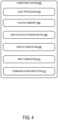
- Fig. 5 schematically shows a non-limiting embodiment of a computing system 400 that can enact one or more of the methods and processes described above.
- Computing system 400 is shown in simplified form.
- Computing system 400 may embody the storage device 12 or host device 200 described above and illustrated in Figs. 1 and 2 .
- Computing system 400 may take the form of one or more personal computers, server computers, tablet computers, home-entertainment computers, network computing devices, gaming devices, mobile computing devices, mobile communication devices (e.g., smart phone), and/or other computing devices, and wearable computing devices such as smart wristwatches and head mounted augmented reality devices.
- Computing system 400 includes a logic processor 402 volatile memory 404, and a non-volatile storage device 406.
- Computing system 400 may optionally include a display subsystem 408, input subsystem 410, communication subsystem 412, and/or other components not shown in Fig. 5.
- Logic processor 402 includes one or more physical devices configured to execute instructions.
- the logic processor may be configured to execute instructions that are part of one or more applications, programs, routines, libraries, objects, components, data structures, or other logical constructs. Such instructions may be implemented to perform a task, implement a data type, transform the state of one or more components, achieve a technical effect, or otherwise arrive at a desired result.
- the logic processor may include one or more physical processors (hardware) configured to execute software instructions. Additionally or alternatively, the logic processor may include one or more hardware logic circuits or firmware devices configured to execute hardware-implemented logic or firmware instructions. Processors of the logic processor 402 may be single-core or multi-core, and the instructions executed thereon may be configured for sequential, parallel, and/or distributed processing. Individual components of the logic processor optionally may be distributed among two or more separate devices, which may be remotely located and/or configured for coordinated processing. Aspects of the logic processor may be virtualized and executed by remotely accessible, networked computing devices configured in a cloud-computing configuration. In such a case, these virtualized aspects are run on different physical logic processors of various different machines, it will be understood.
- Non-volatile storage device 406 includes one or more physical devices configured to hold instructions executable by the logic processors to implement the methods and processes described herein. When such methods and processes are implemented, the state of non-volatile storage device 406 may be transformed-e.g., to hold different data.
- Non-volatile storage device 406 may include physical devices that are removable and/or built-in.
- Non-volatile storage device 406 may include optical memory (e.g., CD, DVD, HD-DVD, etc.), semiconductor memory (e.g., ROM, EPROM, EEPROM, FLASH memory, etc.), and/or magnetic memory (e.g., hard-disk drive, floppy-disk drive, tape drive, MRAM, etc.), or other mass storage device technology.
- Non-volatile storage device 406 may include nonvolatile, dynamic, static, read/write, read-only, sequential-access, location-addressable, file-addressable, and/or content-addressable devices. It will be appreciated that non-volatile storage device 406 is configured to hold instructions even when power is cut to the non-volatile storage device 406.
- Volatile memory 404 may include physical devices that include random access memory. Volatile memory 404 is typically utilized by logic processor 402 to temporarily store information during processing of software instructions. It will be appreciated that volatile memory 404 typically does not continue to store instructions when power is cut to the volatile memory 404.
- logic processor 402, volatile memory 404, and non-volatile storage device 406 may be integrated together into one or more hardware-logic components.
- Such hardware-logic components may include field-programmable gate arrays (FPGAs), program- and application-specific integrated circuits (PASIC / ASICs), program- and application-specific standard products (PSSP / ASSPs), system-on-a-chip (SOC), and complex programmable logic devices (CPLDs), for example.
- FPGAs field-programmable gate arrays
- PASIC / ASICs program- and application-specific integrated circuits
- PSSP / ASSPs program- and application-specific standard products
- SOC system-on-a-chip
- CPLDs complex programmable logic devices
- module may be used to describe an aspect of computing system 400 typically implemented in software by a processor to perform a particular function using portions of volatile memory, which function involves transformative processing that specially configures the processor to perform the function.
- a module, program, or engine may be instantiated via logic processor 402 executing instructions held by non-volatile storage device 406, using portions of volatile memory 404.
- modules, programs, and/or engines may be instantiated from the same application, service, code block, object, library, routine, API, function, etc.
- the same module, program, and/or engine may be instantiated by different applications, services, code blocks, objects, routines, APIs, functions, etc.
- the terms “module,” “program,” and “engine” may encompass individual or groups of executable files, data files, libraries, drivers, scripts, database records, etc.
- display subsystem 408 may be used to present a visual representation of data held by non-volatile storage device 406.
- the visual representation may take the form of a graphical user interface (GUI).
- Display subsystem 408 may include one or more display devices. Such display devices may be combined with logic processor 402, volatile memory 404, and/or non-volatile storage device 406 in a shared enclosure, or such display devices may be peripheral display devices.
- input subsystem 410 may comprise or interface with one or more user-input devices such as a keyboard, mouse, or touch screen.
- user-input devices such as a keyboard, mouse, or touch screen.
- Such componentry may be integrated or peripheral, and the transduction and/or processing of input actions may be handled on- or off-board.
- communication subsystem 412 may be configured to communicatively couple various computing devices described herein with each other, and with other devices.
- Communication subsystem 412 may include wired and/or wireless communication devices compatible with one or more different communication protocols.
- the communication subsystem may be configured for communication via a wireless telephone network, or a wired or wireless local- or wide-area network, such as a HDMI over Wi-Fi connection.
- the communication subsystem may allow computing system 400 to send and/or receive messages to and/or from other devices via a network such as the Internet.
- ZNS zoned namespaces
- the processor being configured to execute a zone writing program to receive zone write commands; and responsive to receiving the zone write commands, execute the zone write commands on the given zone of the non-volatile memory of the storage computing device in an order specified by zone write sequence numbers included in a zone descriptor for the given zone.
- the processor is configured as firmware.
- the processor includes an application specific integrated circuit (ASIC).
- each of the plurality of zones has an associated zone descriptor; and each zone descriptor has associated zone write sequence numbers, which record an order in which zone write commands are issued by a memory controller of a host device.
- the zone write sequence numbers are included in reserved fields of the zone write commands.
- the processor holds zone write commands from a host device in a submission queue; and the processor compares the zone write commands of the submission queue to the zone write sequence numbers.
- the processor is configured as a multi-core processor, and uses a compare-and-swap (CAS) instruction to perform the comparisons in shared memory of the ZNS storage computing device.
- CAS compare-and-swap
- a current zone write sequence number matches a zone write command in the submission queue
- the zone write command is executed by the processor, the current zone write sequence number is incremented by one, and the zone write command is removed from the submission queue.
- the zone write command is held as pending in the submission queue, and a timeout timestamp is attached to the zone write command.
- the processor aborts all the zone write commands in the submission queue.
- Zoned namespaces (ZNS) storage method for executing zone write commands on non-volatile memory comprising a plurality of zones, the method comprising receiving zone write commands; and responsive to receiving the zone write commands, executing the zone write commands on a given zone of the non-volatile memory of a storage device in an order specified by zone write sequence numbers included in a zone descriptor for the given zone.
- the method further comprises retrieving the zone descriptor and the zone write sequence numbers for the given zone from a host device, wherein each of the plurality of zones has an associated zone descriptor; and each zone descriptor has associated zone write sequence numbers, which record an order in which zone write commands are issued by a memory controller of the host device.
- the method further comprises retrieving the zone write sequence numbers from reserved fields of the zone write commands.
- the method further comprises holding zone write commands from a host device in a submission queue; and comparing the zone write commands of the submission queue to the zone write sequence numbers.
- the method further comprises using a compare-and-swap (CAS) instruction to perform the comparisons.
- CAS compare-and-swap
- zone write command in the submission queue has a sequence number which is greater than a current zone write sequence number
- the zone write command is held as pending in the submission queue, and a timeout timestamp is attached to the zone write command.
- a zone write command in the submission queue has a sequence number which is less than a current zone write sequence number, then all the zone write commands in the submission queue are aborted.
- Zoned namespaces storage computing system comprising a storage device comprising non-volatile memory divided into a plurality of zones; and a host device comprising a memory controller, wherein the host device and the storage device store one or a plurality of zone descriptors containing information about one or more of the plurality of zones; the one or the plurality of zone descriptors contain zone write sequence numbers, which record an order in which zone write commands are issued by the memory controller for a given zone of the plurality of zones; the storage device receives the zone write commands; and responsive to receiving the zone write commands, the storage device executes the zone write commands on the given zone of the non-volatile memory of the storage device in an order specified by zone write sequence numbers included in a zone descriptor for the given zone.
- the zone write sequence numbers are included in reserved fields of the zone write commands.
Landscapes
- Engineering & Computer Science (AREA)
- Theoretical Computer Science (AREA)
- Human Computer Interaction (AREA)
- Physics & Mathematics (AREA)
- General Engineering & Computer Science (AREA)
- General Physics & Mathematics (AREA)
- Information Retrieval, Db Structures And Fs Structures Therefor (AREA)
Abstract
Description
- The present disclosure relates to the field of storage and more particularly to a zoned namespaces storage device and system.
- The NVMe (non-volatile memory express) specification is a logical-device interface specification for accessing non-volatile storage media which is attached to a host computing device via a Peripheral Component Interconnect (PCI) Express (PCIe) bus. The NVMe specification may be used with a variety of non-volatile storage media, such as solid state drives (SSDs). One focus of the NVMe specification relates to input/output (I/O) communication between a host device, which may access and/or write to the non-volatile storage media, and a memory device which includes the non-volatile storage media. In this regard, NVMe implements a paired submission queue and completion queue mechanism, with host software on the host device placing commands into the submission queue. Completions are placed onto the associated completion queue by the memory device controller of the storage device.
- An NVMe device implementing the NVMe specification may process write commands in a Relaxed Ordering mechanism, in which write commands sent by a requester are reordered and completed by a completer in an order that is different from the original order in which the write commands were sent.
- This may pose problems in an NVMe device implementing the Zoned Namespaces (ZNS) specification, which requires that zones be written sequentially. Under the ZNS specification, each zone of the device address space has a write pointer which keeps track of the position of the next write. Zone write commands advance the write pointer to the end of the newly written data. Preserving the sequential order of the zone write commands is especially important to ensure that the write pointer is advanced to the appropriate positions in the address space, so that zone write commands are executed at the correct locations in the non-volatile memory.
- Commands may be scrambled out of order in the following situations:
- 1. Command fetch: A controller may fetch submission queue entries from the host memory by sending a memory read request to the host memory. However, the fetched submission queue entries may be scrambled out of order due to various circumstances, including bad link quality.
- 2. Command data transfer: Responsive to receiving a zone write command, the controller may fetch a physical region page (PRP) entry or scatter gather list (SGL) entry to enable a data transfer. However, the resulting data transfer may not preserve the original order of the data.
- 3. Controller-to-firmware Application Program Interface (API): Some controllers use an API like a Host-Tag bitmap for firmware to process the incoming commands. As the bitmap does not contain any order information, the firmware may not preserve the original order of the data.
- 4. Multi-core processing: Some controllers dispatch commands from the same submission queue to different API queues, and then the commands are processed by different cores, which also may lead to commands that are executed out of order.
- In view of the above, a zoned namespaces (ZNS) storage computing device is provided. The ZNS storage computing device comprises a processor, and non-volatile memory comprising a plurality of zones including a given zone. The processor is configured to execute a zone writing program to receive zone write commands, and responsive to receiving the zone write commands, execute the zone write commands on the given zone of the non-volatile memory of the storage computing device in an order specified by zone write sequence numbers included in a zone descriptor for the given zone.
- This Summary is provided to introduce a selection of concepts in a simplified form that are further described below in the Detailed Description. This Summary is not intended to identify key features or essential features of the claimed subject matter, nor is it intended to be used to limit the scope of the claimed subject matter. Furthermore, the claimed subject matter is not limited to implementations that solve any or all disadvantages noted in any part of this disclosure.
-
-
Fig. 1 illustrates a schematic view of a computing system according to an example of the present disclosure. -
Fig. 2 illustrates an expanded schematic view of the storage device of the computing system ofFig. 1 . -
Fig. 3 is a flowchart of a method for writing zone commands on a given zone of non-volatile memory according to an example embodiment of the present disclosure. -
Fig. 4 shows an example computing environment of the present disclosure. - In view of the above issues, the present disclosure describes a system and method for preserving the order in which zone write commands are issued on a NVMe ZNS storage device which is connected to a host computing device via a PCI Express (PCIe) bus.
- Referring to
Fig. 1 , acomputing system 10 comprises astorage device 12 including aprocessor 14,firmware 16,non-volatile memory 18, and a data bus 20 coupled to theprocessor 14 and thenon-volatile memory 18. The processor is configured to execute azone writing program 22 or logic to receive zone writecommands 36, and responsive to receiving the zone writecommands 36, execute the zone writecommands 36 on a given zone of thenon-volatile memory 18. Theprocessor 14 is a microprocessor, which can include an application specific integrated circuit (ASIC). Thefirmware 16 may be configured as permanent software programmed into a read-only memory of thestorage device 12. - The
processor 14 of thestorage device 12 communicates with amemory controller 202 of ahost device 200 via a PCIe bus 204. Thestorage device 12 may be a rack mounted storage platform containing individual solid state drives, in one particular example. Thenon-volatile memory 18 of thestorage device 12 is divided into zoned namespaces, including a plurality ofzones zone non-volatile memory 18 is a contiguous range of logical block addresses that are managed as a single unit. The number ofzones non-volatile memory 18 is not particularly limited, and thenon-volatile memory 18 in the example ofFig. 1 is depicted as having x zones. - The
host device 200 and thestorage device 12 store one or a plurality ofzone descriptor zones non-volatile memory 18 of thestorage device 12. Eachzone associated zone descriptor commands 36 are issued by thememory controller 202 of thehost device 200 for eachzone storage device 12 may retrieve thezone descriptors write sequence numbers command 32 to thehost device 200 to request azone descriptor command 32, thehost device 200 sends one or a plurality ofzone descriptors storage device 12. Accordingly, thestorage device 12 can execute the zone writecommands 36 in an order which is specified by zonewrite sequence numbers zone descriptor zone - Although only two
zone descriptors Fig. 1 , it will be appreciated that theprocessor 14 may retrieve any number of zone descriptors corresponding to the zones of thenon-volatile memory 18 on which zone write commands are to be executed. Thezone descriptors commands 36 may be configured to include the zonewrite sequence numbers storage device 12 may retrieve thezone descriptors sequence numbers - Turning to
Fig. 2 , an expanded view is depicted of thestorage device 12 ofFig. 1 . Each zone writecommand 36 for each zone is assigned a zonewrite sequence number Fig. 2 , the zone writesequence numbers 26a in the zone zerodescriptor 24a comprise writecommands 26a(1)-(4) forzone zero 40a. The zone writesequence numbers 26b in the zone onedescriptor 24b comprise writecommands 26b(1)-(4) for zone one 40b. Forzone zero 40a, the offset0 write command is assigned theSN0 sequence number 26a(1), the offset1 write command is assigned theSN1 sequence number 26a(2), the offset2 write command is assigned theSN2 sequence number 26a(3), and the offset3 write command is assigned theSN3 sequence number 26a(4), so that the offset0, offset1, offset2, and offset3 write commands are executed on the logical block addresses ofzone zero 40a in this specified order. - Similarly, for zone one 40b, the offset0 write command is assigned the
SN0 sequence number 26b(1), the offset1 write command is assigned theSN1 sequence number 26b(2), the offset2 write command is assigned theSN2 sequence number 26b(3), and the offsets write command is assigned theSN3 sequence number 26b(4), so that the offset0, offset1, offset2, and offset3 write commands are executed on the logical block addresses of zone one 40b in this specified order. - Responsive to receiving a zone
open command 34 from thehost device 200, theprocessor 14 opens a given zone on thenon-volatile memory 18 for executing zone write commands. In the example ofFig. 2 , the zoneopen command 34 causes theprocessor 14 to openzone zero 40a and zone one 40b for executing zone writecommands 36. Each zone is assigned a current zonewrite sequence number zone zero 40a is assigned a first current zone writesequence number 30a, and zone one 40b is assigned a second current zone writesequence number 30b. When a given zone is opened, the current zonewrite sequence number processor 14 then receives and holds the zone write commands 36 in asubmission queue 28 preserving an order in which the zone write commands 36 were received by theprocessor 14. The zoneopen command 34 may be configured with a zone write sequencenumber support bit 34a to indicate to thestorage device 12 that that thehost device 200 supports zonewrite sequence numbers - As depicted in the example of
Fig. 2 , the zone commands in thesubmission queue 28 are scrambled due to a bad link quality. Thesubmission queue 28 includes a first zone write command 28(1) specifying offset1 forzone 0, a second zone write command 28(2) specifying offset3 forzone 0, a third zone write command 28(3) specifying offset0 forzone 1, a fourth zone write command 28(4) specifying offset2 forzone 1, a fifth zone write command 28(5) specifying offset0 forzone 0, a sixth zone write command 28(6) specifying offset2 forzone 0, a seventh zone write command 28(7) specifying offset1 forzone 1, and an eighth zone write command 28(8) specifying offset3 forzone 1, in this order. - The
processor 14 then compares the entries of thesubmission queue 28 to the zonewrite sequence numbers zone descriptor write sequence number zone descriptor submission queue 28. Theprocessor 14 may iterate through thesubmission queue 28 in a loop to compare each zone write command in thesubmission queue 28 to the current zonewrite sequence number write sequence number 30a forzone 0 is zero, theprocessor 14 compares the zonewrite sequence number 26a(1) forzone 0 at sequence number zero (SNO) with the first zone write command 28(1) in thesubmission queue 28. When the first zone write command 28(1) does not match the currentwrite sequence number 30a or does not meet the criteria for aborting thesubmission queue 28, then theprocessor 14 compares the currentwrite sequence number 30a to the next zone write command in the submission queue 28: the second zone write command 28(2). When theprocessor 14 is configured as a multi-core processor, then theprocessor 14 may use a compare-and-swap (CAS) instruction to perform the comparisons in shared memory. - The
processor 14 then determines whether the current zonewrite sequence number 30a of thezone descriptor 24a matches the write command in thesubmission queue 28, whether the zone write command in thesubmission queue 28 has a sequence number which is greater than the current zonewrite sequence number 30a of thezone descriptor 24a, whether the write command in thesubmission queue 28 has a sequence number which is less than the current zonewrite sequence number 30a of thezone descriptor 24a, and whether a timeout timestamp attached to a zone write command has expired. - When the current zone
write sequence number 30a of thezone descriptor 24a matches the write command in thesubmission queue 28, then the write command is executed by theprocessor 14, the current zonewrite sequence number 30a is incremented by one, the write command is removed from thesubmission queue 28, and awrite command confirmation 38 or acknowledgment is sent to thehost device 200. For example, when the current zonewrite sequence number 30a is zero, and the fifth zone write command 28(5) of thesubmission queue 28 matches the current zonewrite sequence number 26a(1) at sequence number zero (SN0), then the fifth zone write command 28(5) is executed by theprocessor 14, the current zonewrite sequence number 30a is incremented by one, the fifth zone write command 28(5) is removed from thesubmission queue 28, and awrite command confirmation 38 is sent to thehost device 200. - When the zone write command in the
submission queue 28 has a sequence number which is greater than the current zonewrite sequence number 30a of thezone descriptor 24a, then the write command is held as pending in thesubmission queue 28, and a timeout timestamp is attached to the write command, recording the time at which the write command was held as pending in thesubmission queue 28. For example, when the current zonewrite sequence number 30a is zero, and the first zone write command 28(1) of thesubmission queue 28 has a sequence number of one, which is greater than the current zonewrite sequence number 30a of zero, then the first zone write command 28(1) is held in thesubmission queue 28, and a timeout timestamp is attached to the write command. When a zone write command with a timeout timestamp is not executed by theprocessor 14 within a predetermined time period specified by the timeout stamp, then theprocessor 14 determines that the zone write command has expired, and aborts all the write commands in thesubmission queue 28. - When the write command in the
submission queue 28 has a sequence number which is less than the current zonewrite sequence number 30a of thezone descriptor 24a, then theprocessor 14 aborts all the write commands in thesubmission queue 28. For example, when the current zonewrite sequence number 30a is three, and the zone write command 28(6) in thesubmission queue 28 is two, then theprocessor 14 aborts all the write commands in thesubmission queue 28. - Referring back to
Fig. 1 , operations of asecond storage device 112 are described in detail. In thesecond storage device 112, a processor is configured asfirmware 114 to execute thezone writing program 122. Since the features of thesecond storage device 112 are similar to thefirst storage device 12 with the exception of thefirmware 114, the detailed description thereof is abbreviated here. Like parts in this example are numbered similarly and share their functions with the exception of thefirmware 114, and will not be described again except as below for the sake of brevity. - The
second storage device 112 includesfirmware 114,non-volatile memory 118, and a data bus 120 coupled to thefirmware 114 and thenon-volatile memory 118. Thefirmware 114 is configured to executezone writing program 122 or logic to perform zone write commands 136 on thenon-volatile memory 118 according to thezone writing program 122. Thefirmware 114 may be configured as permanent software programmed into a read-only memory of thestorage device 112. Thehost device 200 and thestorage device 112 store one or a plurality ofzone descriptor zones non-volatile memory 118 of thestorage device 112. - The
firmware 114 of thestorage device 112 communicates with amemory controller 202 of ahost device 200 via a PCIe bus 204. Responsive to receiving a zoneopen command 134 from thehost device 200, thefirmware 114 opens a given zone for executing zone write commands. In the example ofFig. 2 , the zoneopen command 134 causes thefirmware 114 to open zone zero 140a andzone 140b for executing zone write commands 136. When a given zone is opened, thecurrent sequence number firmware 114 then receives and holds the zone write commands 136 in asubmission queue 128 preserving an order in which the zone write commands 136 were received by thefirmware 114. - The
firmware 114 compares the entries of thesubmission queue 128 to the zonewrite sequence numbers zone descriptor write sequence number zone descriptor submission queue 128. When thestorage device 112 is configured as a multi-core processor, then thefirmware 16 may use CAS instruction to perform the comparisons in shared memory. - The
firmware 114 then determines whether the current zonewrite sequence number 130a of thezone descriptor 124a matches the write command in thesubmission queue 128, whether the zone write command in thesubmission queue 128 has a sequence number which is greater than the current zonewrite sequence number 130a of thezone descriptor 124a, whether the write command in thesubmission queue 128 has a sequence number which is less than the current zonewrite sequence number 130a of thezone descriptor 124a, and whether a timeout timestamp attached to a zone write command has expired. - When the current zone
write sequence number 130a of thezone descriptor 124a matches the write command in thesubmission queue 128, then the write command is executed by thefirmware 114, the current zonewrite sequence number 130a is incremented by one, the write command is removed from thesubmission queue 128, and awrite command confirmation 138 or acknowledgment is sent to thehost device 200. - When the write command in the
submission queue 128 has a sequence number which is greater than the current zonewrite sequence number 130a of thezone descriptor 124a, then the write command is held as pending in thesubmission queue 128, and a timeout timestamp is attached to the write command, recording the time at which the write command was held as pending in thesubmission queue 128. When a zone write command with a timeout timestamp is not executed by thefirmware 114 within a predetermined time period, then thefirmware 114 determines that the write command has expired, and aborts all the write commands in thesubmission queue 128. - When the write command in the
submission queue 128 has a sequence number which is less than the current zonewrite sequence number 130a of thezone descriptor 124a, then thefirmware 114 aborts all the write commands in thesubmission queue 128. - The reserved fields of the zone write commands 136 may be configured to include the zone
write sequence numbers open command 134 may be configured with a zone write sequencenumber support bit 134a to indicate to thestorage device 112 that that thehost device 200 supports zonewrite sequence numbers -
Fig. 3 illustrates a flowchart of acomputerized method 300 for executing zone write commands on a given zone of the non-volatile memory of a storage device in an order specified by zone write sequence numbers included in a zone descriptor for the given zone in accordance with a zone writing program. The following description ofcomputerized method 300 is provided with reference to the software and hardware components described above and shown inFigs. 1 and2 . It will be appreciated thatcomputerized method 300 also may be performed in other contexts using other suitable hardware and software components. - At
step 302, zone management receive command is sent to host device. Atstep 304, a zone descriptor and zone write sequence numbers are retrieved from the host device. Each of the plurality of zones of the non-volatile memory of the storage device has an associated zone descriptor, and each zone descriptor has associated zone write sequence numbers, which record an order in which zone write commands are issued by a memory controller of the host device. - At
step 306, a zone open command is received from the host device. Atstep 308, responsive to receiving the zone open command, a given zone is opened on the non-volatile memory for executing zone write commands. Atstep 310, zone write commands are received from the host device. Atstep 312, zone write commands from the host device are held in a submission queue. - At
step 314, the zone write commands of the submission queue are compared to the zone write sequence numbers. It is determined whether the current zone write sequence number of the zone descriptor matches the write command in the submission queue, whether the zone write command in the submission queue has a sequence number which is greater than the current zone write sequence number of the zone descriptor, whether the write command in the submission queue has a sequence number which is less than the current zone write sequence number of the zone descriptor, and whether a timeout timestamp attached to a zone write command has expired. - At
step 316, responsive to determining that the current zone write sequence number of the zone descriptor matches the write command in the submission queue, the zone write command is executed on the given zone of the non-volatile memory of the storage device in an order specified by the zone write sequence numbers included in the zone descriptor for the given zone. Atstep 318, it is determined whether all the zone write commands in the submission queue have been executed. - At
step 328, responsive to determining that all the zone write commands in the submission queue have been executed, a write command confirmation or acknowledgment is sent to the host device, and atstep 330, the zone write operation is terminated. - At
step 320, responsive to determining that all the zone write commands in the submission queue have not been executed, the current zone write sequence number is incremented by one. Atstep 322, the zone write command is removed from the submission queue. Atstep 324, the next zone write command is identified in the submission queue for comparison to the current zone write sequence number, and themethod 300 returns to step 314. - At
step 326, responsive to determining that the write command in the submission queue has a sequence number which is less than the current zone write sequence number of the zone descriptor, or responsive to determining that a timeout timestamp attached to a zone write command has expired, all write commands in the submission queue are aborted. - At
step 332, responsive to determining that the zone write command in the submission queue has a sequence number which is greater than the current zone write sequence number of the zone descriptor, the zone write command is held as pending in the submission queue. Atstep 334, a timeout timestamp is attached to the held zone write command. Atstep 336, the next zone write command is identified in the submission queue for comparison to the current zone write sequence number, and themethod 300 returns to step 314. - The above-described system and method allow zone write commands in an NVMe device implementing the ZNS specification to be executed in the original order in which the write commands were sent by a host device. Accordingly, the original sequential order of the zone write commands can be preserved, and zone write commands can be prevented from being executed out of order in various situations, including command fetches, command data transfers, controller-to-firmware APIs, and multi-core processing.
- In some embodiments, the methods and processes described herein may be tied to a computing system of one or more computing devices. In particular, such methods and processes may be implemented as a computer-application program or service, an application-programming interface (API), a library, and/or other computer-program product.
- Fig. 5 schematically shows a non-limiting embodiment of a
computing system 400 that can enact one or more of the methods and processes described above.Computing system 400 is shown in simplified form.Computing system 400 may embody thestorage device 12 orhost device 200 described above and illustrated inFigs. 1 and2 .Computing system 400 may take the form of one or more personal computers, server computers, tablet computers, home-entertainment computers, network computing devices, gaming devices, mobile computing devices, mobile communication devices (e.g., smart phone), and/or other computing devices, and wearable computing devices such as smart wristwatches and head mounted augmented reality devices. -
Computing system 400 includes alogic processor 402volatile memory 404, and anon-volatile storage device 406.Computing system 400 may optionally include adisplay subsystem 408,input subsystem 410,communication subsystem 412, and/or other components not shown in Fig. 5. -
Logic processor 402 includes one or more physical devices configured to execute instructions. For example, the logic processor may be configured to execute instructions that are part of one or more applications, programs, routines, libraries, objects, components, data structures, or other logical constructs. Such instructions may be implemented to perform a task, implement a data type, transform the state of one or more components, achieve a technical effect, or otherwise arrive at a desired result. - The logic processor may include one or more physical processors (hardware) configured to execute software instructions. Additionally or alternatively, the logic processor may include one or more hardware logic circuits or firmware devices configured to execute hardware-implemented logic or firmware instructions. Processors of the
logic processor 402 may be single-core or multi-core, and the instructions executed thereon may be configured for sequential, parallel, and/or distributed processing. Individual components of the logic processor optionally may be distributed among two or more separate devices, which may be remotely located and/or configured for coordinated processing. Aspects of the logic processor may be virtualized and executed by remotely accessible, networked computing devices configured in a cloud-computing configuration. In such a case, these virtualized aspects are run on different physical logic processors of various different machines, it will be understood. -
Non-volatile storage device 406 includes one or more physical devices configured to hold instructions executable by the logic processors to implement the methods and processes described herein. When such methods and processes are implemented, the state ofnon-volatile storage device 406 may be transformed-e.g., to hold different data. -
Non-volatile storage device 406 may include physical devices that are removable and/or built-in.Non-volatile storage device 406 may include optical memory (e.g., CD, DVD, HD-DVD, etc.), semiconductor memory (e.g., ROM, EPROM, EEPROM, FLASH memory, etc.), and/or magnetic memory (e.g., hard-disk drive, floppy-disk drive, tape drive, MRAM, etc.), or other mass storage device technology.Non-volatile storage device 406 may include nonvolatile, dynamic, static, read/write, read-only, sequential-access, location-addressable, file-addressable, and/or content-addressable devices. It will be appreciated thatnon-volatile storage device 406 is configured to hold instructions even when power is cut to thenon-volatile storage device 406. -
Volatile memory 404 may include physical devices that include random access memory.Volatile memory 404 is typically utilized bylogic processor 402 to temporarily store information during processing of software instructions. It will be appreciated thatvolatile memory 404 typically does not continue to store instructions when power is cut to thevolatile memory 404. - Aspects of
logic processor 402,volatile memory 404, andnon-volatile storage device 406 may be integrated together into one or more hardware-logic components. Such hardware-logic components may include field-programmable gate arrays (FPGAs), program- and application-specific integrated circuits (PASIC / ASICs), program- and application-specific standard products (PSSP / ASSPs), system-on-a-chip (SOC), and complex programmable logic devices (CPLDs), for example. - The terms "module," "program," and "engine" may be used to describe an aspect of
computing system 400 typically implemented in software by a processor to perform a particular function using portions of volatile memory, which function involves transformative processing that specially configures the processor to perform the function. Thus, a module, program, or engine may be instantiated vialogic processor 402 executing instructions held bynon-volatile storage device 406, using portions ofvolatile memory 404. It will be understood that different modules, programs, and/or engines may be instantiated from the same application, service, code block, object, library, routine, API, function, etc. Likewise, the same module, program, and/or engine may be instantiated by different applications, services, code blocks, objects, routines, APIs, functions, etc. The terms "module," "program," and "engine" may encompass individual or groups of executable files, data files, libraries, drivers, scripts, database records, etc. - When included,
display subsystem 408 may be used to present a visual representation of data held bynon-volatile storage device 406. The visual representation may take the form of a graphical user interface (GUI).Display subsystem 408 may include one or more display devices. Such display devices may be combined withlogic processor 402,volatile memory 404, and/ornon-volatile storage device 406 in a shared enclosure, or such display devices may be peripheral display devices. - When included,
input subsystem 410 may comprise or interface with one or more user-input devices such as a keyboard, mouse, or touch screen. Such componentry may be integrated or peripheral, and the transduction and/or processing of input actions may be handled on- or off-board. - When included,
communication subsystem 412 may be configured to communicatively couple various computing devices described herein with each other, and with other devices.Communication subsystem 412 may include wired and/or wireless communication devices compatible with one or more different communication protocols. As non-limiting examples, the communication subsystem may be configured for communication via a wireless telephone network, or a wired or wireless local- or wide-area network, such as a HDMI over Wi-Fi connection. In some embodiments, the communication subsystem may allowcomputing system 400 to send and/or receive messages to and/or from other devices via a network such as the Internet. - The following paragraphs provide additional support for the claims of the subject application. One aspect provides a zoned namespaces (ZNS) storage computing device comprising a processor; and non-volatile memory comprising a plurality of zones including a given zone, the processor being configured to execute a zone writing program to receive zone write commands; and responsive to receiving the zone write commands, execute the zone write commands on the given zone of the non-volatile memory of the storage computing device in an order specified by zone write sequence numbers included in a zone descriptor for the given zone. In this aspect, additionally or alternatively, the processor is configured as firmware. In this aspect, additionally or alternatively, the processor includes an application specific integrated circuit (ASIC). In this aspect, additionally or alternatively, each of the plurality of zones has an associated zone descriptor; and each zone descriptor has associated zone write sequence numbers, which record an order in which zone write commands are issued by a memory controller of a host device. In this aspect, additionally or alternatively, the zone write sequence numbers are included in reserved fields of the zone write commands. In this aspect, additionally or alternatively, the processor holds zone write commands from a host device in a submission queue; and the processor compares the zone write commands of the submission queue to the zone write sequence numbers. In this aspect, additionally or alternatively, the processor is configured as a multi-core processor, and uses a compare-and-swap (CAS) instruction to perform the comparisons in shared memory of the ZNS storage computing device. In this aspect, additionally or alternatively, when a current zone write sequence number matches a zone write command in the submission queue, then the zone write command is executed by the processor, the current zone write sequence number is incremented by one, and the zone write command is removed from the submission queue. In this aspect, additionally or alternatively, when a zone write command in the submission queue has a sequence number which is greater than a current zone write sequence number, then the zone write command is held as pending in the submission queue, and a timeout timestamp is attached to the zone write command. In this aspect, additionally or alternatively, when a zone write command in the submission queue has a sequence number which is less than a current zone write sequence number, then the processor aborts all the zone write commands in the submission queue.
- Another aspect provides a zoned namespaces (ZNS) storage method for executing zone write commands on non-volatile memory comprising a plurality of zones, the method comprising receiving zone write commands; and responsive to receiving the zone write commands, executing the zone write commands on a given zone of the non-volatile memory of a storage device in an order specified by zone write sequence numbers included in a zone descriptor for the given zone. In this aspect, additionally or alternatively, the method further comprises retrieving the zone descriptor and the zone write sequence numbers for the given zone from a host device, wherein each of the plurality of zones has an associated zone descriptor; and each zone descriptor has associated zone write sequence numbers, which record an order in which zone write commands are issued by a memory controller of the host device. In this aspect, additionally or alternatively, the method further comprises retrieving the zone write sequence numbers from reserved fields of the zone write commands. In this aspect, additionally or alternatively, the method further comprises holding zone write commands from a host device in a submission queue; and comparing the zone write commands of the submission queue to the zone write sequence numbers. In this aspect, additionally or alternatively, the method further comprises using a compare-and-swap (CAS) instruction to perform the comparisons. In this aspect, additionally or alternatively, when a current zone write sequence number matches a zone write command in the submission queue, then the zone write command is executed, the current zone write sequence number is incremented by one, and the zone write command is removed from the submission queue. In this aspect, additionally or alternatively, when a zone write command in the submission queue has a sequence number which is greater than a current zone write sequence number, then the zone write command is held as pending in the submission queue, and a timeout timestamp is attached to the zone write command. In this aspect, additionally or alternatively, when a zone write command in the submission queue has a sequence number which is less than a current zone write sequence number, then all the zone write commands in the submission queue are aborted.
- Another aspect provides a zoned namespaces (ZNS) storage computing system comprising a storage device comprising non-volatile memory divided into a plurality of zones; and a host device comprising a memory controller, wherein the host device and the storage device store one or a plurality of zone descriptors containing information about one or more of the plurality of zones; the one or the plurality of zone descriptors contain zone write sequence numbers, which record an order in which zone write commands are issued by the memory controller for a given zone of the plurality of zones; the storage device receives the zone write commands; and responsive to receiving the zone write commands, the storage device executes the zone write commands on the given zone of the non-volatile memory of the storage device in an order specified by zone write sequence numbers included in a zone descriptor for the given zone. In this aspect, additionally or alternatively, the zone write sequence numbers are included in reserved fields of the zone write commands.
- It will be understood that the configurations and/or approaches described herein are exemplary in nature, and that these specific embodiments or examples are not to be considered in a limiting sense, because numerous variations are possible. The specific routines or methods described herein may represent one or more of any number of processing strategies. As such, various acts illustrated and/or described may be performed in the sequence illustrated and/or described, in other sequences, in parallel, or omitted. Likewise, the order of the above-described processes may be changed.
- It will be appreciated that "and/or" as used herein refers to the logical disjunction operation, and thus A and/or B has the following truth table.
A B A and/or B T T T T F T F T T F F F - The subject matter of the present disclosure includes all novel and non-obvious combinations and sub-combinations of the various processes, systems and configurations, and other features, functions, acts, and/or properties disclosed herein, as well as any and all equivalents thereof.
Claims (15)
- A zoned namespaces, ZNS, storage computing device comprising:a processor (14); andnon-volatile memory (18) comprising a plurality of zones (40a, 40b) including a given zone, whereinthe processor (14) is configured to execute a zone writing program to:receive zone write commands (36); andresponsive to receiving the zone write commands (36), execute the zone write commands (36) on the given zone of the non-volatile memory (18) of the storage computing device (12) in an order specified by zone write sequence numbers (24a, 24b) included in a zone descriptor for the given zone.
- The ZNS storage computing device of claim 1, wherein the processor is configured as firmware.
- The ZNS storage computing device of claim 1, wherein the processor includes an application specific integrated circuit, ASIC.
- The ZNS storage computing device of claim 1, whereineach of the plurality of zones has an associated zone descriptor; andeach zone descriptor has associated zone write sequence numbers, which record an order in which zone write commands are issued by a memory controller of a host device.
- The ZNS storage computing device of claim 1, wherein the zone write sequence numbers are included in reserved fields of the zone write commands.
- The ZNS storage computing device of claim 1, whereinthe processor holds zone write commands from a host device in a submission queue; andthe processor compares the zone write commands of the submission queue to the zone write sequence numbers.
- The ZNS storage computing device of claim 6, wherein the processor is configured as a multi-core processor, and uses a compare-and-swap, CAS, instruction to perform the comparisons in shared memory of the ZNS storage computing device, oroptionally, when a current zone write sequence number matches a zone write command in the submission queue, then the zone write command is executed by the processor, the current zone write sequence number is incremented by one, and the zone write command is removed from the submission queue, oroptionally, when a zone write command in the submission queue has a sequence number which is greater than a current zone write sequence number, then the zone write command is held as pending in the submission queue, and a timeout timestamp is attached to the zone write command, oroptionally, when a zone write command in the submission queue has a sequence number which is less than a current zone write sequence number, then the processor aborts all the zone write commands in the submission queue.
- A zoned namespaces, ZNS, storage method for executing zone write commands (36) on non-volatile memory (18) comprising a plurality of zones (40a, 40b), the method comprising:receiving zone write commands (36); andresponsive to receiving the zone write commands (36), executing the zone write commands (36) on a given zone of the non-volatile memory (18) of a storage device (12) in an order specified by zone write sequence numbers (24a, 24b) included in a zone descriptor for the given zone.
- The ZNS storage method of claim 8, further comprising:retrieving the zone descriptor and the zone write sequence numbers for the given zone from a host device, whereineach of the plurality of zones has an associated zone descriptor; andeach zone descriptor has associated zone write sequence numbers, which record an order in which zone write commands are issued by a memory controller of the host device.
- The ZNS storage method of claim 8, further comprising:
retrieving the zone write sequence numbers from reserved fields of the zone write commands. - The ZNS storage method of claim 8, further comprising:holding zone write commands from a host device in a submission queue; andcomparing the zone write commands of the submission queue to the zone write sequence numbers.
- The ZNS storage method of claim 11, further comprising:
using a compare-and-swap, CAS, instruction to perform the comparisons. - The ZNS storage method of claim 11, whereinwhen a current zone write sequence number matches a zone write command in the submission queue, then the zone write command is executed, the current zone write sequence number is incremented by one, and the zone write command is removed from the submission queue, oroptionally, when a zone write command in the submission queue has a sequence number which is greater than a current zone write sequence number, then the zone write command is held as pending in the submission queue, and a timeout timestamp is attached to the zone write command, oroptionally, when a zone write command in the submission queue has a sequence number which is less than a current zone write sequence number, then all the zone write commands in the submission queue are aborted.
- A zoned namespaces, ZNS, storage computing system comprising:a storage device (12) comprising non-volatile memory (18) divided into a plurality of zones (40a, 40b); anda host device (200) comprising a memory controller (202), whereinthe host device (200) and the storage device (12) store one or a plurality of zone descriptors (24a, 24b) containing information about one or more of the plurality of zones (40a, 40b);the one or the plurality of zone descriptors (24a, 24b) contain zone write sequence numbers (26a, 26b), which record an order in which zone write commands (36) are issued by the memory controller (202) for a given zone of the plurality of zones (40a, 40b);the storage device (12) receives the zone write commands (36); andresponsive to receiving the zone write commands (36), the storage device (12) executes the zone write commands (36) on the given zone of the non-volatile memory (18) of the storage device (12) in an order specified by zone write sequence numbers included in a zone descriptor for the given zone.
- The ZNS storage computing system of claim 14, wherein the zone write sequence numbers are included in reserved fields of the zone write commands.
Applications Claiming Priority (1)
| Application Number | Priority Date | Filing Date | Title |
|---|---|---|---|
| US18/189,153 US20230229358A1 (en) | 2023-03-23 | 2023-03-23 | Zoned namespaces storage device and system |
Publications (2)
| Publication Number | Publication Date |
|---|---|
| EP4435581A1 true EP4435581A1 (en) | 2024-09-25 |
| EP4435581B1 EP4435581B1 (en) | 2025-08-06 |
Family
ID=87161862
Family Applications (1)
| Application Number | Title | Priority Date | Filing Date |
|---|---|---|---|
| EP24165284.1A Active EP4435581B1 (en) | 2023-03-23 | 2024-03-21 | Zoned namespaces storage device and system |
Country Status (3)
| Country | Link |
|---|---|
| US (1) | US20230229358A1 (en) |
| EP (1) | EP4435581B1 (en) |
| CN (1) | CN118151849A (en) |
Families Citing this family (2)
| Publication number | Priority date | Publication date | Assignee | Title |
|---|---|---|---|---|
| US12608159B2 (en) * | 2024-02-14 | 2026-04-21 | SanDisk Technologies, Inc. | Efficient sequential write gap processing |
| WO2025179572A1 (en) * | 2024-03-01 | 2025-09-04 | Qualcomm Incorporated | Writing data in zoned storage devices |
Citations (1)
| Publication number | Priority date | Publication date | Assignee | Title |
|---|---|---|---|---|
| WO2021050107A1 (en) * | 2019-09-12 | 2021-03-18 | Western Digital Technologies, Inc. | Non-sequential zoned namespaces |
Family Cites Families (5)
| Publication number | Priority date | Publication date | Assignee | Title |
|---|---|---|---|---|
| US7962780B2 (en) * | 2008-08-22 | 2011-06-14 | International Business Machines Corporation | Command sequence numbering apparatus and method |
| US11017096B2 (en) * | 2018-06-01 | 2021-05-25 | University Of South Florida | Prediction of software vulnerabilities |
| US20200409601A1 (en) * | 2019-06-28 | 2020-12-31 | Western Digital Technologies, Inc. | Hold of Write Commands in Zoned Namespaces |
| US11200161B2 (en) * | 2020-04-20 | 2021-12-14 | Western Digital Technologies, Inc. | Keeping zones open with intermediate padding |
| US11803329B2 (en) * | 2021-11-22 | 2023-10-31 | Netapp, Inc. | Methods and systems for processing write requests in a storage system |
-
2023
- 2023-03-23 US US18/189,153 patent/US20230229358A1/en active Pending
-
2024
- 2024-03-15 CN CN202410301132.1A patent/CN118151849A/en active Pending
- 2024-03-21 EP EP24165284.1A patent/EP4435581B1/en active Active
Patent Citations (1)
| Publication number | Priority date | Publication date | Assignee | Title |
|---|---|---|---|---|
| WO2021050107A1 (en) * | 2019-09-12 | 2021-03-18 | Western Digital Technologies, Inc. | Non-sequential zoned namespaces |
Non-Patent Citations (3)
| Title |
|---|
| ANONYMOUS: "Compare-and-swap - Wikipedia", 21 February 2019 (2019-02-21), pages 1 - 7, XP055883033, Retrieved from the Internet <URL:https://en.wikipedia.org/w/index.php?title=Compare-and-swap&oldid=884339820> [retrieved on 20220124] * |
| BJ�RLING MATIAS: "Zoned Namespaces (ZNS) SSDs: Disrupting the Storage Industry", 22 September 2020 (2020-09-22), XP093124939, Retrieved from the Internet <URL:https://snia.org/sites/default/files/SDC/2020/075-Bj�rling-Zoned-Namespaces-ZNS-SSDs.pdf> [retrieved on 20240129] * |
| MAHESHWARI UMESH UMESH@ALUM MIT EDU: "From blocks to rocks a natural extension of zoned namespaces", PROCEEDINGS OF THE 29TH ACM JOINT MEETING ON EUROPEAN SOFTWARE ENGINEERING CONFERENCE AND SYMPOSIUM ON THE FOUNDATIONS OF SOFTWARE ENGINEERING, ACMPUB27, NEW YORK, NY, USA, 27 July 2021 (2021-07-27), pages 21 - 27, XP058766904, ISBN: 978-1-4503-8563-3, DOI: 10.1145/3465332.3470870 * |
Also Published As
| Publication number | Publication date |
|---|---|
| US20230229358A1 (en) | 2023-07-20 |
| CN118151849A (en) | 2024-06-07 |
| EP4435581B1 (en) | 2025-08-06 |
Similar Documents
| Publication | Publication Date | Title |
|---|---|---|
| EP4435581B1 (en) | Zoned namespaces storage device and system | |
| US10089012B1 (en) | Zero on demand operations based on zeroed chunk tables of storage drive objects stored in main memory | |
| US20180089266A1 (en) | Direct table association in in-memory databases | |
| CN111158939A (en) | Data processing method, data processing device, storage medium and electronic equipment | |
| US11755558B2 (en) | Transaction identifier locking with data row locks | |
| US20130173878A1 (en) | Source-target relations mapping | |
| US8589601B2 (en) | I/O controller and descriptor transfer method | |
| US9471614B2 (en) | Data allocation containers in a partitioned table of a computer database system for holding data based on usage | |
| EP4386566B1 (en) | System and method for allocating memory space | |
| WO2019109514A1 (en) | Datasheet backup method, device, electronic apparatus and medium | |
| US9836239B2 (en) | Recording device and information processing device | |
| US10929347B2 (en) | Defragmenting files having file blocks in multiple point-in-time copies | |
| US10387267B2 (en) | Fast copy using file system block mappings | |
| WO2018194862A1 (en) | File directory synchronization | |
| US20120005441A1 (en) | Copying apparatus, copying method, memory medium, and program | |
| US9778845B2 (en) | File management system | |
| US10996893B2 (en) | Non-volatile storage partition identifier | |
| CN111176726B (en) | Configurable command revocation method and device thereof | |
| US20060047934A1 (en) | Integrated circuit capable of memory access control | |
| CN118778875A (en) | Data storage system, method, device and related equipment | |
| US20230185770A1 (en) | Information processing apparatus, information processing method, and information processing program | |
| EP4604452A1 (en) | Methods and apparatus to manage transmissions between domains and memory | |
| US20220382462A1 (en) | Information processing apparatus, information processing method, and information processing program | |
| EP4202715A1 (en) | Information processing device, information processing method, and information processing program | |
| US9443114B1 (en) | Auto-logging of read/write commands in a storage network |
Legal Events
| Date | Code | Title | Description |
|---|---|---|---|
| PUAI | Public reference made under article 153(3) epc to a published international application that has entered the european phase |
Free format text: ORIGINAL CODE: 0009012 |
|
| STAA | Information on the status of an ep patent application or granted ep patent |
Free format text: STATUS: REQUEST FOR EXAMINATION WAS MADE |
|
| 17P | Request for examination filed |
Effective date: 20240321 |
|
| AK | Designated contracting states |
Kind code of ref document: A1 Designated state(s): AL AT BE BG CH CY CZ DE DK EE ES FI FR GB GR HR HU IE IS IT LI LT LU LV MC ME MK MT NL NO PL PT RO RS SE SI SK SM TR |
|
| GRAP | Despatch of communication of intention to grant a patent |
Free format text: ORIGINAL CODE: EPIDOSNIGR1 |
|
| STAA | Information on the status of an ep patent application or granted ep patent |
Free format text: STATUS: GRANT OF PATENT IS INTENDED |
|
| RIC1 | Information provided on ipc code assigned before grant |
Ipc: G06F 3/06 20060101AFI20250423BHEP |
|
| INTG | Intention to grant announced |
Effective date: 20250512 |
|
| GRAS | Grant fee paid |
Free format text: ORIGINAL CODE: EPIDOSNIGR3 |
|
| GRAA | (expected) grant |
Free format text: ORIGINAL CODE: 0009210 |
|
| STAA | Information on the status of an ep patent application or granted ep patent |
Free format text: STATUS: THE PATENT HAS BEEN GRANTED |
|
| P01 | Opt-out of the competence of the unified patent court (upc) registered |
Free format text: CASE NUMBER: APP_28797/2025 Effective date: 20250617 |
|
| AK | Designated contracting states |
Kind code of ref document: B1 Designated state(s): AL AT BE BG CH CY CZ DE DK EE ES FI FR GB GR HR HU IE IS IT LI LT LU LV MC ME MK MT NL NO PL PT RO RS SE SI SK SM TR |
|
| REG | Reference to a national code |
Ref country code: GB Ref legal event code: FG4D |
|
| REG | Reference to a national code |
Ref country code: CH Ref legal event code: EP |
|
| REG | Reference to a national code |
Ref country code: IE Ref legal event code: FG4D |
|
| REG | Reference to a national code |
Ref country code: DE Ref legal event code: R096 Ref document number: 602024000393 Country of ref document: DE |
|
| REG | Reference to a national code |
Ref country code: NL Ref legal event code: MP Effective date: 20250806 |
|
| PG25 | Lapsed in a contracting state [announced via postgrant information from national office to epo] |
Ref country code: IS Free format text: LAPSE BECAUSE OF FAILURE TO SUBMIT A TRANSLATION OF THE DESCRIPTION OR TO PAY THE FEE WITHIN THE PRESCRIBED TIME-LIMIT Effective date: 20251206 |
|
| PG25 | Lapsed in a contracting state [announced via postgrant information from national office to epo] |
Ref country code: NO Free format text: LAPSE BECAUSE OF FAILURE TO SUBMIT A TRANSLATION OF THE DESCRIPTION OR TO PAY THE FEE WITHIN THE PRESCRIBED TIME-LIMIT Effective date: 20251106 |
|
| REG | Reference to a national code |
Ref country code: LT Ref legal event code: MG9D |
|
| PG25 | Lapsed in a contracting state [announced via postgrant information from national office to epo] |
Ref country code: PT Free format text: LAPSE BECAUSE OF FAILURE TO SUBMIT A TRANSLATION OF THE DESCRIPTION OR TO PAY THE FEE WITHIN THE PRESCRIBED TIME-LIMIT Effective date: 20251209 |
|
| PG25 | Lapsed in a contracting state [announced via postgrant information from national office to epo] |
Ref country code: FI Free format text: LAPSE BECAUSE OF FAILURE TO SUBMIT A TRANSLATION OF THE DESCRIPTION OR TO PAY THE FEE WITHIN THE PRESCRIBED TIME-LIMIT Effective date: 20250806 |
|
| PG25 | Lapsed in a contracting state [announced via postgrant information from national office to epo] |
Ref country code: HR Free format text: LAPSE BECAUSE OF FAILURE TO SUBMIT A TRANSLATION OF THE DESCRIPTION OR TO PAY THE FEE WITHIN THE PRESCRIBED TIME-LIMIT Effective date: 20250806 Ref country code: NL Free format text: LAPSE BECAUSE OF FAILURE TO SUBMIT A TRANSLATION OF THE DESCRIPTION OR TO PAY THE FEE WITHIN THE PRESCRIBED TIME-LIMIT Effective date: 20250806 |
|
| PG25 | Lapsed in a contracting state [announced via postgrant information from national office to epo] |
Ref country code: GR Free format text: LAPSE BECAUSE OF FAILURE TO SUBMIT A TRANSLATION OF THE DESCRIPTION OR TO PAY THE FEE WITHIN THE PRESCRIBED TIME-LIMIT Effective date: 20251107 |
|
| PG25 | Lapsed in a contracting state [announced via postgrant information from national office to epo] |
Ref country code: SE Free format text: LAPSE BECAUSE OF FAILURE TO SUBMIT A TRANSLATION OF THE DESCRIPTION OR TO PAY THE FEE WITHIN THE PRESCRIBED TIME-LIMIT Effective date: 20250806 |
|
| PG25 | Lapsed in a contracting state [announced via postgrant information from national office to epo] |
Ref country code: LV Free format text: LAPSE BECAUSE OF FAILURE TO SUBMIT A TRANSLATION OF THE DESCRIPTION OR TO PAY THE FEE WITHIN THE PRESCRIBED TIME-LIMIT Effective date: 20250806 |
|
| PG25 | Lapsed in a contracting state [announced via postgrant information from national office to epo] |
Ref country code: PL Free format text: LAPSE BECAUSE OF FAILURE TO SUBMIT A TRANSLATION OF THE DESCRIPTION OR TO PAY THE FEE WITHIN THE PRESCRIBED TIME-LIMIT Effective date: 20250806 Ref country code: BG Free format text: LAPSE BECAUSE OF FAILURE TO SUBMIT A TRANSLATION OF THE DESCRIPTION OR TO PAY THE FEE WITHIN THE PRESCRIBED TIME-LIMIT Effective date: 20250806 |
|
| PG25 | Lapsed in a contracting state [announced via postgrant information from national office to epo] |
Ref country code: RS Free format text: LAPSE BECAUSE OF FAILURE TO SUBMIT A TRANSLATION OF THE DESCRIPTION OR TO PAY THE FEE WITHIN THE PRESCRIBED TIME-LIMIT Effective date: 20251106 |
|
| PG25 | Lapsed in a contracting state [announced via postgrant information from national office to epo] |
Ref country code: ES Free format text: LAPSE BECAUSE OF FAILURE TO SUBMIT A TRANSLATION OF THE DESCRIPTION OR TO PAY THE FEE WITHIN THE PRESCRIBED TIME-LIMIT Effective date: 20250806 |
|
| REG | Reference to a national code |
Ref country code: AT Ref legal event code: MK05 Ref document number: 1822647 Country of ref document: AT Kind code of ref document: T Effective date: 20250806 |
|
| PG25 | Lapsed in a contracting state [announced via postgrant information from national office to epo] |
Ref country code: SM Free format text: LAPSE BECAUSE OF FAILURE TO SUBMIT A TRANSLATION OF THE DESCRIPTION OR TO PAY THE FEE WITHIN THE PRESCRIBED TIME-LIMIT Effective date: 20250806 |
|
| PG25 | Lapsed in a contracting state [announced via postgrant information from national office to epo] |
Ref country code: DK Free format text: LAPSE BECAUSE OF FAILURE TO SUBMIT A TRANSLATION OF THE DESCRIPTION OR TO PAY THE FEE WITHIN THE PRESCRIBED TIME-LIMIT Effective date: 20250806 |
|
| PGFP | Annual fee paid to national office [announced via postgrant information from national office to epo] |
Ref country code: DE Payment date: 20260320 Year of fee payment: 3 |
|
| PG25 | Lapsed in a contracting state [announced via postgrant information from national office to epo] |
Ref country code: AT Free format text: LAPSE BECAUSE OF FAILURE TO SUBMIT A TRANSLATION OF THE DESCRIPTION OR TO PAY THE FEE WITHIN THE PRESCRIBED TIME-LIMIT Effective date: 20250806 |
|
| PG25 | Lapsed in a contracting state [announced via postgrant information from national office to epo] |
Ref country code: IT Free format text: LAPSE BECAUSE OF FAILURE TO SUBMIT A TRANSLATION OF THE DESCRIPTION OR TO PAY THE FEE WITHIN THE PRESCRIBED TIME-LIMIT Effective date: 20250806 |
|
| PGFP | Annual fee paid to national office [announced via postgrant information from national office to epo] |
Ref country code: FR Payment date: 20260119 Year of fee payment: 3 |
|
| PG25 | Lapsed in a contracting state [announced via postgrant information from national office to epo] |
Ref country code: CZ Free format text: LAPSE BECAUSE OF FAILURE TO SUBMIT A TRANSLATION OF THE DESCRIPTION OR TO PAY THE FEE WITHIN THE PRESCRIBED TIME-LIMIT Effective date: 20250806 |
|
| PG25 | Lapsed in a contracting state [announced via postgrant information from national office to epo] |
Ref country code: EE Free format text: LAPSE BECAUSE OF FAILURE TO SUBMIT A TRANSLATION OF THE DESCRIPTION OR TO PAY THE FEE WITHIN THE PRESCRIBED TIME-LIMIT Effective date: 20250806 Ref country code: SK Free format text: LAPSE BECAUSE OF FAILURE TO SUBMIT A TRANSLATION OF THE DESCRIPTION OR TO PAY THE FEE WITHIN THE PRESCRIBED TIME-LIMIT Effective date: 20250806 |