EP4435508A1 - Integrated circuit for generating a frequency comb signal, optical system and test and measurement device - Google Patents
Integrated circuit for generating a frequency comb signal, optical system and test and measurement device Download PDFInfo
- Publication number
- EP4435508A1 EP4435508A1 EP23163326.4A EP23163326A EP4435508A1 EP 4435508 A1 EP4435508 A1 EP 4435508A1 EP 23163326 A EP23163326 A EP 23163326A EP 4435508 A1 EP4435508 A1 EP 4435508A1
- Authority
- EP
- European Patent Office
- Prior art keywords
- optical
- integrated circuit
- generation unit
- signal
- photodiode
- Prior art date
- Legal status (The legal status is an assumption and is not a legal conclusion. Google has not performed a legal analysis and makes no representation as to the accuracy of the status listed.)
- Pending
Links
- 230000003287 optical effect Effects 0.000 title claims abstract description 152
- 238000012360 testing method Methods 0.000 title claims abstract description 16
- 238000005259 measurement Methods 0.000 title claims abstract description 14
- 239000000463 material Substances 0.000 claims description 18
- 229910052581 Si3N4 Inorganic materials 0.000 claims description 5
- GQYHUHYESMUTHG-UHFFFAOYSA-N lithium niobate Chemical compound [Li+].[O-][Nb](=O)=O GQYHUHYESMUTHG-UHFFFAOYSA-N 0.000 claims description 5
- HQVNEWCFYHHQES-UHFFFAOYSA-N silicon nitride Chemical compound N12[Si]34N5[Si]62N3[Si]51N64 HQVNEWCFYHHQES-UHFFFAOYSA-N 0.000 claims description 5
- 101150071746 Pbsn gene Proteins 0.000 claims 1
- 230000010354 integration Effects 0.000 abstract description 3
- 239000004065 semiconductor Substances 0.000 description 22
- 239000000758 substrate Substances 0.000 description 14
- 230000009021 linear effect Effects 0.000 description 11
- 238000010586 diagram Methods 0.000 description 10
- 238000001228 spectrum Methods 0.000 description 8
- 230000008901 benefit Effects 0.000 description 5
- 238000000034 method Methods 0.000 description 5
- 238000005516 engineering process Methods 0.000 description 4
- 238000004519 manufacturing process Methods 0.000 description 4
- 238000004891 communication Methods 0.000 description 3
- 230000009022 nonlinear effect Effects 0.000 description 3
- RLLPVAHGXHCWKJ-IEBWSBKVSA-N (3-phenoxyphenyl)methyl (1s,3s)-3-(2,2-dichloroethenyl)-2,2-dimethylcyclopropane-1-carboxylate Chemical compound CC1(C)[C@H](C=C(Cl)Cl)[C@@H]1C(=O)OCC1=CC=CC(OC=2C=CC=CC=2)=C1 RLLPVAHGXHCWKJ-IEBWSBKVSA-N 0.000 description 2
- 238000013459 approach Methods 0.000 description 2
- 238000012512 characterization method Methods 0.000 description 2
- 230000014509 gene expression Effects 0.000 description 2
- 230000007246 mechanism Effects 0.000 description 2
- 230000008569 process Effects 0.000 description 2
- 239000002210 silicon-based material Substances 0.000 description 2
- 230000003595 spectral effect Effects 0.000 description 2
- 238000004544 sputter deposition Methods 0.000 description 2
- JBRZTFJDHDCESZ-UHFFFAOYSA-N AsGa Chemical compound [As]#[Ga] JBRZTFJDHDCESZ-UHFFFAOYSA-N 0.000 description 1
- 238000002231 Czochralski process Methods 0.000 description 1
- 229910003327 LiNbO3 Inorganic materials 0.000 description 1
- XUIMIQQOPSSXEZ-UHFFFAOYSA-N Silicon Chemical compound [Si] XUIMIQQOPSSXEZ-UHFFFAOYSA-N 0.000 description 1
- 238000007792 addition Methods 0.000 description 1
- 238000004458 analytical method Methods 0.000 description 1
- 230000005540 biological transmission Effects 0.000 description 1
- 239000013078 crystal Substances 0.000 description 1
- 238000013016 damping Methods 0.000 description 1
- 230000002950 deficient Effects 0.000 description 1
- 230000001419 dependent effect Effects 0.000 description 1
- 238000000151 deposition Methods 0.000 description 1
- 238000011161 development Methods 0.000 description 1
- 230000018109 developmental process Effects 0.000 description 1
- 229910003460 diamond Inorganic materials 0.000 description 1
- 239000010432 diamond Substances 0.000 description 1
- 230000000694 effects Effects 0.000 description 1
- 238000005530 etching Methods 0.000 description 1
- 230000007274 generation of a signal involved in cell-cell signaling Effects 0.000 description 1
- 238000001459 lithography Methods 0.000 description 1
- 239000000155 melt Substances 0.000 description 1
- 239000000203 mixture Substances 0.000 description 1
- 238000012986 modification Methods 0.000 description 1
- 230000004048 modification Effects 0.000 description 1
- 229910021421 monocrystalline silicon Inorganic materials 0.000 description 1
- 239000002245 particle Substances 0.000 description 1
- 230000000737 periodic effect Effects 0.000 description 1
- 238000012913 prioritisation Methods 0.000 description 1
- 238000012545 processing Methods 0.000 description 1
- 230000001902 propagating effect Effects 0.000 description 1
- 238000005070 sampling Methods 0.000 description 1
- 229910052710 silicon Inorganic materials 0.000 description 1
- 239000010703 silicon Substances 0.000 description 1
- HBMJWWWQQXIZIP-UHFFFAOYSA-N silicon carbide Chemical compound [Si+]#[C-] HBMJWWWQQXIZIP-UHFFFAOYSA-N 0.000 description 1
- 229910010271 silicon carbide Inorganic materials 0.000 description 1
- 239000007787 solid Substances 0.000 description 1
- 230000007480 spreading Effects 0.000 description 1
- 238000003892 spreading Methods 0.000 description 1
- 230000002123 temporal effect Effects 0.000 description 1
- 238000012546 transfer Methods 0.000 description 1
- 230000032258 transport Effects 0.000 description 1
- 230000001960 triggered effect Effects 0.000 description 1
Images



Classifications
-
- G—PHYSICS
- G02—OPTICS
- G02F—OPTICAL DEVICES OR ARRANGEMENTS FOR THE CONTROL OF LIGHT BY MODIFICATION OF THE OPTICAL PROPERTIES OF THE MEDIA OF THE ELEMENTS INVOLVED THEREIN; NON-LINEAR OPTICS; FREQUENCY-CHANGING OF LIGHT; OPTICAL LOGIC ELEMENTS; OPTICAL ANALOGUE/DIGITAL CONVERTERS
- G02F1/00—Devices or arrangements for the control of the intensity, colour, phase, polarisation or direction of light arriving from an independent light source, e.g. switching, gating or modulating; Non-linear optics
- G02F1/35—Non-linear optics
- G02F1/353—Frequency conversion, i.e. wherein a light beam is generated with frequency components different from those of the incident light beams
-
- G—PHYSICS
- G02—OPTICS
- G02F—OPTICAL DEVICES OR ARRANGEMENTS FOR THE CONTROL OF LIGHT BY MODIFICATION OF THE OPTICAL PROPERTIES OF THE MEDIA OF THE ELEMENTS INVOLVED THEREIN; NON-LINEAR OPTICS; FREQUENCY-CHANGING OF LIGHT; OPTICAL LOGIC ELEMENTS; OPTICAL ANALOGUE/DIGITAL CONVERTERS
- G02F1/00—Devices or arrangements for the control of the intensity, colour, phase, polarisation or direction of light arriving from an independent light source, e.g. switching, gating or modulating; Non-linear optics
- G02F1/35—Non-linear optics
- G02F1/3511—Self-focusing or self-trapping of light; Light-induced birefringence; Induced optical Kerr-effect
- G02F1/3513—Soliton propagation
-
- G—PHYSICS
- G02—OPTICS
- G02F—OPTICAL DEVICES OR ARRANGEMENTS FOR THE CONTROL OF LIGHT BY MODIFICATION OF THE OPTICAL PROPERTIES OF THE MEDIA OF THE ELEMENTS INVOLVED THEREIN; NON-LINEAR OPTICS; FREQUENCY-CHANGING OF LIGHT; OPTICAL LOGIC ELEMENTS; OPTICAL ANALOGUE/DIGITAL CONVERTERS
- G02F1/00—Devices or arrangements for the control of the intensity, colour, phase, polarisation or direction of light arriving from an independent light source, e.g. switching, gating or modulating; Non-linear optics
- G02F1/35—Non-linear optics
- G02F1/3511—Self-focusing or self-trapping of light; Light-induced birefringence; Induced optical Kerr-effect
-
- G—PHYSICS
- G02—OPTICS
- G02F—OPTICAL DEVICES OR ARRANGEMENTS FOR THE CONTROL OF LIGHT BY MODIFICATION OF THE OPTICAL PROPERTIES OF THE MEDIA OF THE ELEMENTS INVOLVED THEREIN; NON-LINEAR OPTICS; FREQUENCY-CHANGING OF LIGHT; OPTICAL LOGIC ELEMENTS; OPTICAL ANALOGUE/DIGITAL CONVERTERS
- G02F1/00—Devices or arrangements for the control of the intensity, colour, phase, polarisation or direction of light arriving from an independent light source, e.g. switching, gating or modulating; Non-linear optics
- G02F1/35—Non-linear optics
- G02F1/3501—Constructional details or arrangements of non-linear optical devices, e.g. shape of non-linear crystals
- G02F1/3503—Structural association of optical elements, e.g. lenses, with the non-linear optical device
-
- G—PHYSICS
- G02—OPTICS
- G02F—OPTICAL DEVICES OR ARRANGEMENTS FOR THE CONTROL OF LIGHT BY MODIFICATION OF THE OPTICAL PROPERTIES OF THE MEDIA OF THE ELEMENTS INVOLVED THEREIN; NON-LINEAR OPTICS; FREQUENCY-CHANGING OF LIGHT; OPTICAL LOGIC ELEMENTS; OPTICAL ANALOGUE/DIGITAL CONVERTERS
- G02F1/00—Devices or arrangements for the control of the intensity, colour, phase, polarisation or direction of light arriving from an independent light source, e.g. switching, gating or modulating; Non-linear optics
- G02F1/35—Non-linear optics
- G02F1/3501—Constructional details or arrangements of non-linear optical devices, e.g. shape of non-linear crystals
- G02F1/3507—Arrangements comprising two or more nonlinear optical devices
-
- G—PHYSICS
- G02—OPTICS
- G02F—OPTICAL DEVICES OR ARRANGEMENTS FOR THE CONTROL OF LIGHT BY MODIFICATION OF THE OPTICAL PROPERTIES OF THE MEDIA OF THE ELEMENTS INVOLVED THEREIN; NON-LINEAR OPTICS; FREQUENCY-CHANGING OF LIGHT; OPTICAL LOGIC ELEMENTS; OPTICAL ANALOGUE/DIGITAL CONVERTERS
- G02F1/00—Devices or arrangements for the control of the intensity, colour, phase, polarisation or direction of light arriving from an independent light source, e.g. switching, gating or modulating; Non-linear optics
- G02F1/35—Non-linear optics
- G02F1/355—Non-linear optics characterised by the materials used
- G02F1/3551—Crystals
-
- H—ELECTRICITY
- H01—ELECTRIC ELEMENTS
- H01S—DEVICES USING THE PROCESS OF LIGHT AMPLIFICATION BY STIMULATED EMISSION OF RADIATION [LASER] TO AMPLIFY OR GENERATE LIGHT; DEVICES USING STIMULATED EMISSION OF ELECTROMAGNETIC RADIATION IN WAVE RANGES OTHER THAN OPTICAL
- H01S3/00—Lasers, i.e. devices using stimulated emission of electromagnetic radiation in the infrared, visible or ultraviolet wave range
- H01S3/005—Optical devices external to the laser cavity, specially adapted for lasers, e.g. for homogenisation of the beam or for manipulating laser pulses, e.g. pulse shaping
- H01S3/0085—Modulating the output, i.e. the laser beam is modulated outside the laser cavity
-
- H—ELECTRICITY
- H01—ELECTRIC ELEMENTS
- H01S—DEVICES USING THE PROCESS OF LIGHT AMPLIFICATION BY STIMULATED EMISSION OF RADIATION [LASER] TO AMPLIFY OR GENERATE LIGHT; DEVICES USING STIMULATED EMISSION OF ELECTROMAGNETIC RADIATION IN WAVE RANGES OTHER THAN OPTICAL
- H01S3/00—Lasers, i.e. devices using stimulated emission of electromagnetic radiation in the infrared, visible or ultraviolet wave range
- H01S3/09—Processes or apparatus for excitation, e.g. pumping
- H01S3/091—Processes or apparatus for excitation, e.g. pumping using optical pumping
- H01S3/094—Processes or apparatus for excitation, e.g. pumping using optical pumping by coherent light
- H01S3/094076—Pulsed or modulated pumping
-
- H—ELECTRICITY
- H01—ELECTRIC ELEMENTS
- H01S—DEVICES USING THE PROCESS OF LIGHT AMPLIFICATION BY STIMULATED EMISSION OF RADIATION [LASER] TO AMPLIFY OR GENERATE LIGHT; DEVICES USING STIMULATED EMISSION OF ELECTROMAGNETIC RADIATION IN WAVE RANGES OTHER THAN OPTICAL
- H01S3/00—Lasers, i.e. devices using stimulated emission of electromagnetic radiation in the infrared, visible or ultraviolet wave range
- H01S3/10—Controlling the intensity, frequency, phase, polarisation or direction of the emitted radiation, e.g. switching, gating, modulating or demodulating
- H01S3/11—Mode locking; Q-switching; Other giant-pulse techniques, e.g. cavity dumping
-
- H—ELECTRICITY
- H03—ELECTRONIC CIRCUITRY
- H03B—GENERATION OF OSCILLATIONS, DIRECTLY OR BY FREQUENCY-CHANGING, BY CIRCUITS EMPLOYING ACTIVE ELEMENTS WHICH OPERATE IN A NON-SWITCHING MANNER; GENERATION OF NOISE BY SUCH CIRCUITS
- H03B17/00—Generation of oscillations using radiation source and detector, e.g. with interposed variable obturator
-
- H—ELECTRICITY
- H04—ELECTRIC COMMUNICATION TECHNIQUE
- H04B—TRANSMISSION
- H04B10/00—Transmission systems employing electromagnetic waves other than radio-waves, e.g. infrared, visible or ultraviolet light, or employing corpuscular radiation, e.g. quantum communication
- H04B10/50—Transmitters
- H04B10/501—Structural aspects
- H04B10/506—Multiwavelength transmitters
-
- H—ELECTRICITY
- H04—ELECTRIC COMMUNICATION TECHNIQUE
- H04B—TRANSMISSION
- H04B10/00—Transmission systems employing electromagnetic waves other than radio-waves, e.g. infrared, visible or ultraviolet light, or employing corpuscular radiation, e.g. quantum communication
- H04B10/50—Transmitters
- H04B10/508—Pulse generation, e.g. generation of solitons
-
- G—PHYSICS
- G02—OPTICS
- G02F—OPTICAL DEVICES OR ARRANGEMENTS FOR THE CONTROL OF LIGHT BY MODIFICATION OF THE OPTICAL PROPERTIES OF THE MEDIA OF THE ELEMENTS INVOLVED THEREIN; NON-LINEAR OPTICS; FREQUENCY-CHANGING OF LIGHT; OPTICAL LOGIC ELEMENTS; OPTICAL ANALOGUE/DIGITAL CONVERTERS
- G02F2203/00—Function characteristic
- G02F2203/25—Frequency chirping of an optical modulator; Arrangements or methods for the pre-set or tuning thereof
-
- G—PHYSICS
- G02—OPTICS
- G02F—OPTICAL DEVICES OR ARRANGEMENTS FOR THE CONTROL OF LIGHT BY MODIFICATION OF THE OPTICAL PROPERTIES OF THE MEDIA OF THE ELEMENTS INVOLVED THEREIN; NON-LINEAR OPTICS; FREQUENCY-CHANGING OF LIGHT; OPTICAL LOGIC ELEMENTS; OPTICAL ANALOGUE/DIGITAL CONVERTERS
- G02F2203/00—Function characteristic
- G02F2203/54—Optical pulse train (comb) synthesizer
-
- G—PHYSICS
- G02—OPTICS
- G02F—OPTICAL DEVICES OR ARRANGEMENTS FOR THE CONTROL OF LIGHT BY MODIFICATION OF THE OPTICAL PROPERTIES OF THE MEDIA OF THE ELEMENTS INVOLVED THEREIN; NON-LINEAR OPTICS; FREQUENCY-CHANGING OF LIGHT; OPTICAL LOGIC ELEMENTS; OPTICAL ANALOGUE/DIGITAL CONVERTERS
- G02F2203/00—Function characteristic
- G02F2203/56—Frequency comb synthesizer
Definitions
- the present invention relates to an integrated circuit, in particular a photonic integrated circuit, for generating an electrical and/or optical frequency comb signal.
- the present invention further relates to an optical system and a test and measurement device.
- phase- and amplitude-calibration of spectrum analyzers or oscilloscopes a known reference is often necessary for providing a faster phase and amplitude calibration. This calibration should further be done preferably onsite and not only by means of a factory alignment.
- a so-called comb signal such as a Dirac comb
- the Dirac comb also known as shah function, impulse train or sampling function
- the Dirac comb describes a periodic sequence of Dirac impulses that has the shape of a comb.
- the Dirac comb is often used in signal processing by means of Fourier analysis. In the time domain the Dirac comb represents a train of Dirac pulses which result in the frequency domain to equidistant "pickets" of known amplitude and phase.
- the bandwidth or "picket" with the highest frequency is usually limited.
- a smart cancelling out sequence such as a so-called PRBS-sequence
- a pulsed laser together with a photo diode is employed. This leads to comparably great bandwidths in the range of 100 GHz, however, it results in comparably small power per "picket".
- the frequency comb generation device combines the optical generation of the Dirac train and the cancelling out mechanism of the Dirac pulses in the optical domain and as such combines the benefits of a high bandwidth and at the same time a high output power.
- the present invention provides an integrated circuit having the features of claim 1 and/or by an optical system having the features of claim 14 and/or by a test and measurement device having the features of claim 15.
- the present invention is based on the idea to provide a Kerr-ring for the generation of an optical frequency comb signal. It is the use of this Kerr-ring for the optical frequency comb generation that made integration possible.
- a Kerr-ring denotes a circular type optical waveguide.
- a Kerr-ring is a kind of a non-linear ring resonator within an optical integrated circuit that has nonlinear properties. Due to these nonlinear properties, a short, stable non-linear pulse is generated within the ring resonator. This pulse is also known as soliton or solitary wave.
- a soliton or solitary wave is a self-reinforcing wave packet that maintains its shape while it propagates at a constant velocity. Solitons are caused by a cancellation of nonlinear and dispersive effects in the medium.
- the present invention aims to miniaturize the know concepts for the generation of high frequency comb signals, such as the one described in the technical background.
- all components or at least most of them fit on a single semiconductor chip. This enables significantly higher repetition rates and much lower form factors as in presently known systems.
- the same material system is used for the integrated circuit or optical integrated circuit system.
- any kind of semiconductor material may be used, such as a silicon based materials, in particular monocrystalline silicon, silicon carbide, silicon nitride (Si 3 N 4 ), or non silicon-based material systems, such as lithium niobate (LiNbOs) or gallium arsenide (GaAs).
- a diamond based material may be used.
- test and measurement device may be any optical test and measurement apparatus, a network analyzer, an oscilloscope, a wireless communication tester.
- the invention may also be implemented in or used for signal generators, broadband amplifiers, radio system components, etc.
- the integrated circuit further comprises an optical modulator.
- the optical modulator is preferably integrated in the same semiconductor substrate of the pulse generation unit and is further connected to the pulse generation unit for receiving the generated optical comb signal.
- the optical modulator is configured to generate a modulated optical comb signal based on a modulation control signal.
- the repetition rate can be modified, for example, by only allowing every second pulse of a 100 MHz signal to pass by suitable attenuation, a finer spectrum or repetition rate of, for example, 50 MHz is obtained.
- lithium niobate (LiNbO 3 ) or silicon nitride can be used a preferred material system for the Kerr-ring or Kerr-mircorings.
- Lithium niobate is a transparent, crystalline solid that may be grown from a melt by the Czochralski process. Its single crystals are an important material for optical waveguides, mobile phones, piezoelectric sensors, optical modulators and various other linear and non-linear optical applications. Lithium niobate is sometimes referred to linobate. Additionally, the material of the Kerr-ring may also be silicon nitride.
- the Kerr-ring of the pulse generation unit and/or the optical modulator are completely or at least partially integrated within the material of the semiconductor substrate.
- the Kerr-ring may be produced using commonly known semiconductor manufacturing technologies, such as implanting, doping, lithography, etching, sputtering, etc.
- the Kerr-ring and/or the optical modulator are provided and thus fixedly attached on a surface of the semiconductor substrate.
- the Kerr-ring may be deposited or bonded on the surface for example by deposition techniques, such as sputtering and bonding, respectively.
- At least two Kerr-rings are provided.
- the at least two Kerr-rings may be arranged in parallel to each other. This kind of redundancy allows manufacturing tolerances to be compensated for in a very simple manner and thus order ensure a high signal quality an.
- the at least two Kerr-rings may be arranged in cascade or parallel to each other.
- the integrated circuit further comprises an integrated laser, which is configured to generate the optical high frequency signal for the pulse generation unit.
- the integrated laser is a continuous-wave (CW) laser.
- CW laser emits a light wave of constant intensity.
- the CW laser emits a light wave with a wavelength of 800nm or 1550nm..
- the integrated circuit further comprises a sequence generation unit connected to a control input of the optical modulator.
- the sequence generation is configured to generate the modulation control signal for controlling the optical modulator.
- the sequence generation unit is integrated in the same semiconductor material of the optical modulator and the Kerr-ring of the pulse generation unit. Consequently, all optical components of the test and measuring device - or at least most of them - fit on a single semiconductor chip.
- the sequence generation unit is configured to receive a control signal on the basis of which the sequence generation unit produces the modulation control signal.
- the received control signal may comprise a sequence reset information and/or an information related to the sequence configuration.
- the sequence generation unit is configured to generate a PRBS (Pseudorandom Binary Sequence) signal.
- the pseudorandom binary sequence that can take the values +1 and -1, is a binary signal that approximates the spectrum of white noise and that may be generated by a deterministic random number generator.
- the advantage of the PRBS is the reproducibility of the signal. It is used in communications engineering for code division multiplexing, band spreading, encryption and transmission channel checking, and the like.
- a PRBS can be generated with a linear feedback shift register.
- the PRBS signal generated by the sequence generation unit is part of the modulation control signal and is used for controlling the modulation of the optical modulator.
- the modulation control signal may also comprise equally distanced "1" within “0", a combination of the PRBS with the equally distanced "1" within “0".
- the modulation control signal may also be any arbitrary sequence of "0" and "1".
- the PRBS sequence provides a repeating bit sequence that has certain settable properties. For example, it can be set that the PRBS changes every 15 bits. This results in a corresponding number of additional comb lines of the same amplitude in the characteristic curve such that a finer repetition rate or spectrum is possible.
- the sequence generation unit is configured to operate the optical modulator in a divider mode and/or in an arbitrary mode.
- the sequence generation unit is configured to generate at least one modulation control signal that causes the optical modulator to generate modulated optical comb signals having two different power levels, such as “0" and “1", or preferably more than two different power levels, such as “0", "1” and “0,5". Additionally or alternatively, the sequence generation unit is configured to generate at least one modulation control signal that causes the optical modulator to generate modulated optical comb signals having at least two discrete time shifts. in this way, the delay of the modulation signal can be controlled.
- the sequence generation unit further comprises at least one control input for configuring and controlling the operation of the sequence generation unit.
- the control input of the sequence generation unit is coupled preferably to the pulse generation unit, a reset unit, a sequence configuration unit and/or an external terminal for receiving an externally generated control signal.
- the integrated circuit according to the present invention further comprises in one aspect one first photodiode for generating an electrical comb signal from the modulated optical comb signal.
- the first photodiode that is preferably a broadband photodiode.
- the photodiode generates very fast, broadband electrical pulses when triggered with a repetition rate of, for example, 100 MHz of the optical laser. In this way, a characteristic curve is obtained in the electrical spectrum every 100 MHz, which has a known phase.
- the integrated circuit may comprise at least one second photodiode that is arranged in parallel to the first photodiode.
- the second photodiode is for example of the same type as the first photodiode, e.g. a broadband photodiode, or a narrowband photodiode.
- the first and second photodiodes are preferably integrated within the same semiconductor material.
- the integrated circuit according to the present invention further comprises at least one optical splitter which may be connected downstream the optical modulator and an optical output terminal connected to the optical splitter.
- the splitter may be used for splitting the modulated optical comb signal between an internal signal provided to at least one photodiode within the semiconductor substrate and an external signal provided to an external device, e.g. an external photodiode.
- At least one further optical modulator is provided connected to the pulse generation unit for receiving the generated optical comb signal.
- the further optical modulator which may be identical or at least similar to the optical modulator is connected to or connectable to different photodiode as the optical modulator, in particular via an output terminal to an external photodiode. Additionally or alternatively, the further optical modulator is configured to receive another modulating control signal or the same modulation signal from the sequence generation unit.
- At least one second photodiode connected to the sequence generation unit is provided.
- the sequence generation unit is configured to generate a timing trigger signal for the second photodiode every time a new sequence is generated.
- At least one third photodiode directly connected to the output terminal of the pulse generation unit is provided.
- the third photodiode is used for providing an electrical clock signal or reference signal based on the non-modulated optical comb signal.
- the integrated circuit comprises a phased-locked loop circuit, which is configured to control the frequency of the pulse generation unit and/or of the integrated laser.
- the integrated circuit comprises an external optical input port for receiving an external optical signal and a switching unit.
- the switching unit In a first switching mode the switching unit is configured to connect the optical modulator (and/or further optical modulator) to a first photodiode, and in a second switching mode the switching unit is configured to connect the external optical input port to the first photodiode.
- At least one input terminal for receiving a control signal for controlling the operation of the sequence generation unit and/or for receiving a reference clock signal is provided.
- the integrated circuit 10 may comprise an optical modulator 15 (shown in dotted lines in Fig. 1 ), whichis connected to the pulse generation unit 11, and which is integrated in the same semiconductor substrate 12.
- the integrated circuit 10 shown in Figs. 1, 1A is a so-called photonic integrated circuit (PIC) or integrated optical circuit.
- PIC photonic integrated circuit
- a PIC is a microchip containing two or more photonic components, which form a functional circuit. This technology detects, generates, transports, and processes light. PIC utilize photons (or light particles) as opposed to electrons that are utilized by electric or electronic integrated circuits (ICs).
- the Kerr-ring 20 consists of a linear light guide section 21 and a circular light guide section 22. Both light guide sections 21, 22 are connected to each other at a contact section 23. One end 24 of the linear light guide section 21 functions as an input terminal and the second end 25 functions as an output terminal. The input terminal 24 is used for receiving an optical high frequency signal X1.
- the high frequency signal X1 propagates along the linear light guide section 21 until the contact section 23 is reached. At the contact section 23, at least a portion X1a of the high frequency signal X1 branches towards the circular light guide section 22 while the remaining portion of the high frequency signal X1 keeps propagating along the linear light guide section 21.
- the branched off signal enters the circular light guide section 22 and continues to propagate around the circular light guide section 22 with suitable energy input. Due to non-linear properties of the material of the light guide in connection with the refractive index at the walls of the circular light guide section 22, a pulsed wave signal is generated which continues to propagate around in the circular light guide section 22 as a pulsed wave in the time domain. In the frequency domain, this results in the desired frequency comb.
- This pulsed wave signal X1b reenters the linear light guide section 21 at the contact section 23 such that at the output terminal 25 the pulsed wave signal X2 having the desired frequency comb characteristic is provided.
- Fig. 3 shows a block diagram of a further embodiment of an integrated circuit 10 according to the present invention.
- the integrated circuit 10 comprises the pulse generation unit 11 that comprises the integrated Kerr-ring 20, the optical modulator 15, a sequence generation unit 30 and a photodiode 31.
- the input terminal 24 of the pulse generation unit 11 is used for receiving an optical high frequency signal X1 that is for example generated by an external light source (not shown in Fig. 3 ), such as a laser.
- the pulse generation unit 11 is connected via its output terminal 25 to the optical modulator 15.
- the optical modulator 15 comprises a control terminal 32 that is connected to the sequence generation unit 30.
- the sequence generation unit 30, which is integrated in the same semiconductor substrate, is configured to generate a modulation control signal X3.
- This modulation control signal X3 is used to control the modulation characteristics within the optical modulator 15.
- the optical modulator 15 which receives via (output) terminal 25 the optical pulsed wave signal X2 is configured to generate a modulated optical comb signal X4 based on the modulation control signal X3.
- the generated modulated optical comb signal X4 is provided to the photodiode 31 connected downstream of the optical modulator 15.
- the photodiode 31, which is integrated in the same semiconductor substrate, is preferably a broadband photodiode and is configured to emit an electrical signal X5 that shows the desired high frequency comb characteristic.
- the sequence generation unit 30 is configured to generate a PRBS signal X3 having predefined PRBS bit sequence. In PRBS mode, the sequence generation unit 30 generates the PRBS control signal in such a way that each pulse is passed. With a repetition rate of 100 MHz, a spectral line for the optical comb signal is thus obtained in the spectrum every 100 MHz.
- the sequence generation unit 30 may also be operated to support a divider mode.
- the divider mode only one pulse is passed ("1") followed by a predefined number of non-passed or suppressed pulses ("0").
- the sequence generation unit 30 generates a control signal such to divide the frequency of the repetition rate. For example, by allowing to pass only every second pulse, a frequency of 50 MHz can be set at a repetition rate of 100 MHz, and by allowing to pass every third pulse, a frequency of 33,3 MHz can be set at a repetition rate of 100 MHz. That is, setting a predefined amount of "0" following a "1" allows a desired frequency raster to be set.
- This may be implemented by a comparable simple logic circuit within the sequence generation unit 30, such as an up-counter or a down-counter.
- the sequence generation unit 30 may also be operated to support an arbitrary mode.
- the arbitrary mode In the arbitrary mode, a specific bit sequence of a given length is defined. This makes it possible to generate a fully flexible, user-defined frequency raster at a given repetition rate.
- the arbitrary mode may typically be not implemented by means of a simple logic device, since one usually would need at least a memory device for this purpose. Therefore, the corresponding circuitry is usually arranged externally to the integrated circuit 10. Due to the high setting flexibility of the arbitrary mode, the arbitrary mode typically covers the PRBS mode and the divider mode either.
- Fig. 4 shows a block diagram of an embodiment of an optical system 40 according to the present invention.
- the optical system 40 comprises, in particular, an integrated circuit 10.
- the integrated circuit 10 in Fig. 4 comprises a light source 41, a PLL 42 and two further photodiodes 43, 44.
- the light source 41 is an integrated optical source 41, which can be designed, for example, as a continuous-wave laser.
- the light source 41 is directly coupled to the pulse generation unit 11 via the terminal 24 and is configured to generate the optical high frequency signal X1 for the pulse generation unit 11.
- the phased-locked loop (PLL) 42 is coupled with its input side to the output terminal 25 of the pulse generation unit 11 and with its output side to corresponding control inputs of the light source 41 and the pulse generation unit 11. This enables the PLL to control the wavelength of the optical signal X1 generated by the integrated light source 41 and/or to control the frequency of the pulsed wave signal X2 generated by the pulse generation unit 11, respectively. Employing the PLL 42 ensures that an exact repetition rate of the optical signal is set for use in the modulator 15 or sequence generator 30.
- the pulsed wave signal X2 is fed into the sequence generation unit 30.
- the two further photodiodes 43, 44 may be narrowband photodiodes. In a preferred embodiment, however, the two photodiodes 43, 44 are of the same type as photodiode 31. According to a particular preferred implementation, all photodiodes 31, 43, 44 are broadband photodiodes. This way, one and the same semiconductor technology process may be applied for the production of all photodiodes 31, 43, 44 which is cost efficient.
- One of the photodiodes 44 is connected to the sequence generation unit 30 for receiving a trigger signal X10.
- the sequence generation unit 30 generates this trigger signal X10 every time the (PRBS) sequence is started again.
- the photodiode 44 is then configured to emit a corresponding electrical trigger signal X7, which indicates when the sequence is repeated and thus provides a timing information.
- This trigger signal X7 may be used in an external network analyser or spectral analyser for obtaining an absolute phase reference between the control signal X3 and the electrical signal X5 and a delay information of the signals through a device under test (DUT).
- the other photodiode 43 is connected via the output terminal 25 to the pulse generation unit 11.
- Photodiode 43 is configured to emit an electrical output signal X8 based on the original optical signal X2, which indicates the original repetition rate and thus provides a clock reference.
- the original optical signal X2 is fed out as a clock signal, which can then be evaluated by an external device such as a spectrum analyzer or network analyser (not shown in Fig. 4 ).
- an external device such as a spectrum analyzer or network analyser (not shown in Fig. 4 ).
- These external devices need this clock information as a reference to know on which system clock the integrated circuit 10 is operating.
- Fig. 5 shows a block diagram of a further embodiment of an optical system 40 according to the present invention.
- the optical system 40 in Fig. 5 further comprises a reset unit 46 and a configuration unit 47 which are both coupled to a control interface 48 of the sequence generation unit 30.
- the configuration unit 46 is configured to generate a reset signal X11 that comprises a sequence reset information. This makes it possible to reset the setting set in the sequence generation unit 30, for example to a default setting.
- the configuration unit 47 is configured to generate a configuration signal X12 that comprises an information related to the sequence configuration. This makes it possible to set a specific operating mode with which the sequence generation unit 30 is operated, e.g. a PRBS mode, a divider mode, an arbitrary mode or any other user defined mode.
- a specific operating mode e.g. a PRBS mode, a divider mode, an arbitrary mode or any other user defined mode.
- the configuration unit 46 and the configuration unit 47 are arranged outside the integrated circuit 10, in a preferred embodiment they may also be integrated within the integrated circuit 10.
- the PLL 42 comprises a clock input terminal 50, which is connected to an external clock generator 45.
- the external clock generator 45 is configured to provide a reference frequency X6 for the PLL 42.
- the optical system 40 also comprises a unit 49, which is connected via an input terminal 51 to the integrated circuit 10.
- the unit 49 is configured to generate an external reference pulse signal X9 that may be provided to the photodiode 31.
- This pulse signal X9 is configured such to allow diode characterization of photodiode 31.
- the integrated circuit 10 comprises a switch 52.
- the two input terminals of the switch 52 are connected to the optical modulator 15.
- the output terminal of the switch 52 is connected to the photodiode 31. In this way, photodiode 31 may be operated in a normal operation mode based on the modulated optical comb signal X4 and in diode characterization mode based on the reference pulse signal X9.
- Fig. 6 shows a block diagram of a further embodiment of an optical system 40 according to the present invention.
- a splitter 53 is provided between the optical modulator 15 and the photodiode 31.
- the splitter 53 is configured to split feed the modulated optical comb signal X4 either to photodiode 31 or via an output terminal 54 to an externally arranged further photodiode 55.
- This allows the modulated signal not to be led out of the integrated circuit 10 via the integrated photodiode 31, which is advantageous if, for example, the integrated photodiode 31 is defective, too inaccurate or cannot be used for high-precision applications due to manufacturing tolerances.
- the external photodiode 55 which may be optimized for the specific application can be used.
- a redundancy may be used for at least one of the photodiodes 31, 43, 44, for example by providing one or mode additional photodiodes which are arranged parallel to the corresponding photodiodes 31, 43, 44.
- Fig. 7 shows a block diagram of an embodiment of a test and measurement device 60 according to the present invention.
- the test and measurement device 60 comprises an optical system 40 such as the one shown in Fig. 4 .
- the test and measurement device 60 can alternatively also comprise only an integrated circuit 10 (in Fig. 5 shown in dotted lines) such as the one shown in any of the Figs. 1, 1A , 3 , 4 .
- the test and measurement device 50 may be a spectrum analyser, a network analyzer, an oscilloscope, a wireless communication tester or the like.
- the invention may also be implemented in or used for signal generators, broadband amplifiers, radio system components, etc.
- connections between various elements as shown and described with respect to the drawings may be a type of connection suitable to transfer optical and/or electrical signals from or to the respective nodes, units or devices, for example via intermediate devices. Accordingly, unless implied or stated otherwise the connections may for example be direct connections or indirect connections.
- any reference signs shall not be construed as limiting the claim.
- the word “comprising” does not exclude the presence of other elements or steps then those listed in a claim.
- the terms "a” or “an”, as used herein, are defined as one or more than one.
- the use of introductory phrases such as “at least one” and “one or more” in the claims should not be construed to imply that the introduction of another claim element by the indefinite articles “a” or “an” limits any particular claim containing such introduced claim element to inventions containing only one such element, even when the same claim includes the introductory phrases “one or more” or “at least one” and indefinite articles such as “a” or “an.” The same holds true for the use of definite articles.
Landscapes
- Physics & Mathematics (AREA)
- Nonlinear Science (AREA)
- Optics & Photonics (AREA)
- Electromagnetism (AREA)
- General Physics & Mathematics (AREA)
- Engineering & Computer Science (AREA)
- Chemical & Material Sciences (AREA)
- Crystallography & Structural Chemistry (AREA)
- Plasma & Fusion (AREA)
- Signal Processing (AREA)
- Computer Networks & Wireless Communication (AREA)
- Optical Modulation, Optical Deflection, Nonlinear Optics, Optical Demodulation, Optical Logic Elements (AREA)
- Photometry And Measurement Of Optical Pulse Characteristics (AREA)
Abstract
The present invention relates to an integrated circuit, in particular a photonic integrated circuit, for generating an electrical and/or optical frequency comb signal, the integrated circuit comprising: a pulse generation unit comprising an input port for receiving an optical high frequency signal. The present invention provides a Kerr-ring for the generation of an optical frequency comb signal. The use of the Kerr-ring for the optical frequency comb generation makes the integration possible. The present invention further relates to an optical system and a test and measurement device.
Description
- The present invention relates to an integrated circuit, in particular a photonic integrated circuit, for generating an electrical and/or optical frequency comb signal. The present invention further relates to an optical system and a test and measurement device.
- For phase- and amplitude-calibration of spectrum analyzers or oscilloscopes, a known reference is often necessary for providing a faster phase and amplitude calibration. This calibration should further be done preferably onsite and not only by means of a factory alignment.
- For the generation of a known reference for phase- and amplitude-calibration, a so-called comb signal, such as a Dirac comb, can be used. The Dirac comb (also known as shah function, impulse train or sampling function) describes a periodic sequence of Dirac impulses that has the shape of a comb. The Dirac comb is often used in signal processing by means of Fourier analysis. In the time domain the Dirac comb represents a train of Dirac pulses which result in the frequency domain to equidistant "pickets" of known amplitude and phase. When using a baseband comb, the bandwidth or "picket" with the highest frequency is usually limited.
- Another challenge is the power of each of these "pickets". There is often the need for a very fine frequency grid, however, with a finer frequency grid, the repetition frequency in the time domain is lower and thus fewer Dirac impulses contribute to the total power.
- This can be overcome by using a very high repetition frequency of the Dirac pulses in the time domain (e.g. in the range of 2-10 GHz) and employing a smart canceling out mechanism for damping or cancelling a good portion of the impulses of the Dirac comb. When employing a smart cancelling out sequence (such as a so-called PRBS-sequence), this results in a very fine frequency grid with "pickets" with known amplitude and phase.
- According to another approach for the generation of the electrical train of Dirac pulses, a pulsed laser together with a photo diode is employed. This leads to comparably great bandwidths in the range of 100 GHz, however, it results in comparably small power per "picket".
-
US 10,707,968 B2 - Presently existing optical signal generation devices, such as described above, were miniaturized only to a limited extent, mainly because the currently used optical devices, such as lasers, cannot or can only with great difficulty be integrated in a semiconductor material.
- Against this background, there is a need for an optimized generation of a high frequency comb signal.
- Accordingly, the present invention provides an integrated circuit having the features of
claim 1 and/or by an optical system having the features ofclaim 14 and/or by a test and measurement device having the features ofclaim 15. - According thereto, there is provided:
- An integrated circuit, in particular a photonic integrated circuit, for generating an electrical and/or optical frequency comb signal, the integrated circuit comprising: a pulse generation unit comprising an input port for receiving an optical high frequency signal wherein the pulse generation unit comprises at least one Kerr-ring which is arranged and configured such to generate an optical comb signal from the received optical high frequency signal.
- An optical system, the optical system comprising: at least one integrated circuit according to the present invention, and at least one optical component which is connected to the integrated circuit via an optical or electrical interface, wherein the at least one optical component comprises at least one of the following: an external laser connected via an optical input terminal to the pulse generation unit of the integrated circuit and which is configured to generate an optical high frequency signal; at least one external photodiode connected via an optical output terminal to the integrated circuit.
- A test and measurement device comprising the integrated circuit according to the present invention and/or the optical system according to the present invention.
- The present invention is based on the idea to provide a Kerr-ring for the generation of an optical frequency comb signal. It is the use of this Kerr-ring for the optical frequency comb generation that made integration possible.
- A Kerr-ring denotes a circular type optical waveguide. In particular, a Kerr-ring is a kind of a non-linear ring resonator within an optical integrated circuit that has nonlinear properties. Due to these nonlinear properties, a short, stable non-linear pulse is generated within the ring resonator. This pulse is also known as soliton or solitary wave. A soliton or solitary wave is a self-reinforcing wave packet that maintains its shape while it propagates at a constant velocity. Solitons are caused by a cancellation of nonlinear and dispersive effects in the medium.
- Summarizing the result, the present invention aims to miniaturize the know concepts for the generation of high frequency comb signals, such as the one described in the technical background. Preferably, all components or at least most of them fit on a single semiconductor chip. This enables significantly higher repetition rates and much lower form factors as in presently known systems.
- Furthermore, by integration of the Kerr-ring into a specific semiconductor material, it is now possible to provide comparably small and therefore significantly cheaper devices for the generation of high frequency comb signals.
- For a particular preferred embodiment, the same material system is used for the integrated circuit or optical integrated circuit system. For the substrate of the integrated circuit and as such for the material system, any kind of semiconductor material may be used, such as a silicon based materials, in particular monocrystalline silicon, silicon carbide, silicon nitride (Si3N4), or non silicon-based material systems, such as lithium niobate (LiNbOs) or gallium arsenide (GaAs). Additionally, a diamond based material may be used. However, it may also be productive for some embodiments if different material systems which may comprise a mixture or combination of the above mentions materials are used for the different components of the optical integrated circuit and/or the optical system.
- The test and measurement device according to the present invention may be any optical test and measurement apparatus, a network analyzer, an oscilloscope, a wireless communication tester. The invention may also be implemented in or used for signal generators, broadband amplifiers, radio system components, etc.
- Advantageous configurations and developments emerge from the further dependent claims and from the description with reference to the figures of the drawings.
- In a particular preferred embodiment, the integrated circuit further comprises an optical modulator. The optical modulator is preferably integrated in the same semiconductor substrate of the pulse generation unit and is further connected to the pulse generation unit for receiving the generated optical comb signal. The optical modulator is configured to generate a modulated optical comb signal based on a modulation control signal. Using the modulation technique, the repetition rate can be modified, for example, by only allowing every second pulse of a 100 MHz signal to pass by suitable attenuation, a finer spectrum or repetition rate of, for example, 50 MHz is obtained.
- In a particular preferred embodiment, lithium niobate (LiNbO3) or silicon nitride can be used a preferred material system for the Kerr-ring or Kerr-mircorings. Lithium niobate is a transparent, crystalline solid that may be grown from a melt by the Czochralski process. Its single crystals are an important material for optical waveguides, mobile phones, piezoelectric sensors, optical modulators and various other linear and non-linear optical applications. Lithium niobate is sometimes referred to linobate. Additionally, the material of the Kerr-ring may also be silicon nitride.
- In one embodiment, the Kerr-ring of the pulse generation unit and/or the optical modulator are completely or at least partially integrated within the material of the semiconductor substrate. For this embodiment, the Kerr-ring may be produced using commonly known semiconductor manufacturing technologies, such as implanting, doping, lithography, etching, sputtering, etc. In an alternative embodiment, the Kerr-ring and/or the optical modulator are provided and thus fixedly attached on a surface of the semiconductor substrate. For this embodiment, the Kerr-ring may be deposited or bonded on the surface for example by deposition techniques, such as sputtering and bonding, respectively.
- In a particular preferred embodiment, at least two Kerr-rings are provided. In particular, the at least two Kerr-rings may be arranged in parallel to each other. This kind of redundancy allows manufacturing tolerances to be compensated for in a very simple manner and thus order ensure a high signal quality an. Alternatively or additionally, the at least two Kerr-rings may be arranged in cascade or parallel to each other.
- In one particular preferred embodiment, the integrated circuit further comprises an integrated laser, which is configured to generate the optical high frequency signal for the pulse generation unit. Preferably, the integrated laser is a continuous-wave (CW) laser. Unlike conventional pulse lasers, a CW laser emits a light wave of constant intensity. In the present example, the CW laser emits a light wave with a wavelength of 800nm or 1550nm..
- In one further and particular preferred embodiment, the integrated circuit further comprises a sequence generation unit connected to a control input of the optical modulator. The sequence generation is configured to generate the modulation control signal for controlling the optical modulator. In a further preferred embodiment, the sequence generation unit is integrated in the same semiconductor material of the optical modulator and the Kerr-ring of the pulse generation unit. Consequently, all optical components of the test and measuring device - or at least most of them - fit on a single semiconductor chip.
- In one aspect of the invention, the sequence generation unit is configured to receive a control signal on the basis of which the sequence generation unit produces the modulation control signal. The received control signal may comprise a sequence reset information and/or an information related to the sequence configuration.
- In a particular preferred configuration, the sequence generation unit is configured to generate a PRBS (Pseudorandom Binary Sequence) signal. The pseudorandom binary sequence, that can take the values +1 and -1, is a binary signal that approximates the spectrum of white noise and that may be generated by a deterministic random number generator. The advantage of the PRBS is the reproducibility of the signal. It is used in communications engineering for code division multiplexing, band spreading, encryption and transmission channel checking, and the like. A PRBS can be generated with a linear feedback shift register. The PRBS signal generated by the sequence generation unit is part of the modulation control signal and is used for controlling the modulation of the optical modulator. Instead of a PRBS signal, the modulation control signal may also comprise equally distanced "1" within "0", a combination of the PRBS with the equally distanced "1" within "0". The modulation control signal may also be any arbitrary sequence of "0" and "1". The PRBS sequence provides a repeating bit sequence that has certain settable properties. For example, it can be set that the PRBS changes every 15 bits. This results in a corresponding number of additional comb lines of the same amplitude in the characteristic curve such that a finer repetition rate or spectrum is possible.
- According to an additional or alternative configuration, the sequence generation unit is configured to operate the optical modulator in a divider mode and/or in an arbitrary mode.
- According to a further aspect, the sequence generation unit is configured to generate at least one modulation control signal that causes the optical modulator to generate modulated optical comb signals having two different power levels, such as "0" and "1", or preferably more than two different power levels, such as "0", "1" and "0,5". Additionally or alternatively, the sequence generation unit is configured to generate at least one modulation control signal that causes the optical modulator to generate modulated optical comb signals having at least two discrete time shifts. in this way, the delay of the modulation signal can be controlled.
- According to still another aspect, the sequence generation unit further comprises at least one control input for configuring and controlling the operation of the sequence generation unit. The control input of the sequence generation unit is coupled preferably to the pulse generation unit, a reset unit, a sequence configuration unit and/or an external terminal for receiving an externally generated control signal.
- The integrated circuit according to the present invention further comprises in one aspect one first photodiode for generating an electrical comb signal from the modulated optical comb signal. The first photodiode that is preferably a broadband photodiode. The photodiode generates very fast, broadband electrical pulses when triggered with a repetition rate of, for example, 100 MHz of the optical laser. In this way, a characteristic curve is obtained in the electrical spectrum every 100 MHz, which has a known phase. The integrated circuit may comprise at least one second photodiode that is arranged in parallel to the first photodiode. The second photodiode is for example of the same type as the first photodiode, e.g. a broadband photodiode, or a narrowband photodiode. The first and second photodiodes are preferably integrated within the same semiconductor material.
- The integrated circuit according to the present invention further comprises at least one optical splitter which may be connected downstream the optical modulator and an optical output terminal connected to the optical splitter. The splitter may be used for splitting the modulated optical comb signal between an internal signal provided to at least one photodiode within the semiconductor substrate and an external signal provided to an external device, e.g. an external photodiode.
- According to another configuration, at least one further optical modulator is provided connected to the pulse generation unit for receiving the generated optical comb signal. The further optical modulator, which may be identical or at least similar to the optical modulator is connected to or connectable to different photodiode as the optical modulator, in particular via an output terminal to an external photodiode. Additionally or alternatively, the further optical modulator is configured to receive another modulating control signal or the same modulation signal from the sequence generation unit. By employing a further optical modulator, a redundancy is provided for the output signals, which, in case the regular optical modulator is not working properly, is preferred.
- According to still another configuration, at least one second photodiode connected to the sequence generation unit is provided. The sequence generation unit is configured to generate a timing trigger signal for the second photodiode every time a new sequence is generated.
- According to another configuration, at least one third photodiode directly connected to the output terminal of the pulse generation unit is provided. The third photodiode is used for providing an electrical clock signal or reference signal based on the non-modulated optical comb signal.
- According to a preferred configuration, the integrated circuit comprises a phased-locked loop circuit, which is configured to control the frequency of the pulse generation unit and/or of the integrated laser.
- According to a further configuration, the integrated circuit comprises an external optical input port for receiving an external optical signal and a switching unit. In a first switching mode the switching unit is configured to connect the optical modulator (and/or further optical modulator) to a first photodiode, and in a second switching mode the switching unit is configured to connect the external optical input port to the first photodiode.
- In a preferred aspect, at least one input terminal for receiving a control signal for controlling the operation of the sequence generation unit and/or for receiving a reference clock signal is provided.
- The above embodiments can be combined with each other as desired, if useful. Further possible embodiments, further configurations and implementations of the invention also include combinations, not explicitly mentioned, of features of the invention described herein with respect to the embodiments. In particular, the skilled person will thereby also add individual aspects as improvements or additions to the respective basic form of the present invention.
- For a more comprehensive understanding of the invention and the advantages thereof, exemplary embodiments of the invention are explained in more detail in the following description with reference to the accompanying drawing figures, in which like reference characters designate like parts and in which:
- Fig. 1
- shows a cross section view illustrating a generic embodiment of the integrated circuit according to the present invention;
- Fig. 1A
- shows a cross section view illustrating a further generic embodiment of the integrated circuit according to the present invention;
- Fig. 2
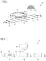
- shows a preferred embodiment of a pulse generation unit formed as a Kerr-ring;
- Fig. 3
- shows a block diagram of a further embodiment of an integrated circuit according to the present invention;
- Fig. 4
- shows a block diagram of an embodiment of an optical system according to the present invention; and
- Fig. 5
- shows a block diagram of a further embodiment of an optical system according to the present invention;
- Fig. 6
- shows a block diagram of a further embodiment of an optical system according to the present invention;
- Fig. 7
- shows a block diagram of an embodiment of a test and measurement device according to the present invention.
- The accompanying drawings are included to provide a fur-ther understanding of the present invention and are incorporated in and constitute a part of this specification. The drawings illustrate particular embodiments of the invention and together with the description serve to explain the principles of the invention. Other embodiments of the invention and many of the resulting advantages of the invention will be readily appreciated, as they become better understood with reference to the following detailed description.
- It will be appreciated that common and/or well understood elements that may be useful or necessary in a commercially feasible embodiment are not necessarily depicted in order to facilitate a more abstracted view of the embodiments. The elements of the drawings are not necessarily illustrated to scale relative to each other. It will further be appreciated that certain actions and/or steps in an embodiment of a method may be described or depicted in a particular order of occurrences while those skilled in the art will understand that such specificity with respect to sequence is not actually required. It will also be under-stood that the terms and expressions used in the present specification have the ordinary meaning as is accorded to such terms and expressions with respect to their corresponding respective areas of inquiry and study, except where specific meanings have otherwise been set forth herein.
-
Figs. 1, 1A show cross section views illustrating generic embodiments of theintegrated circuit 10 according to the present invention. - In
Fig. 1 , theintegrated circuit 10 for generating a frequency comb signal is denoted byreference numeral 10. Theintegrated circuit 10 comprises amongst other components (not shown inFig. 1 ) apulse generation unit 11 that comprises at least one Kerr-ring. - According to the present invention, the
pulse generation unit 11 and thus its at least one Kerr-ring is completely integrated and thus embedded within asemiconductor substrate 12 using known semiconductor technologies. Thesemiconductor substrate 12 can be a silicon substrate. - In another embodiment shown in
Fig. 1A , thepulse generation unit 11 and thus its Kerr-ring is attached via anon-detachable connection 13 on asurface 14 of thesemiconductor substrate 12. Thenon-detachable connection 13 may be a bonding connection, a thermally grown material, a deposited material or the like. - In an additional embodiment the
integrated circuit 10 may comprise an optical modulator 15 (shown in dotted lines inFig. 1 ), whichis connected to thepulse generation unit 11, and which is integrated in thesame semiconductor substrate 12. - In a preferred embodiment, the
integrated circuit 10 shown inFigs. 1, 1A is a so-called photonic integrated circuit (PIC) or integrated optical circuit. A PIC is a microchip containing two or more photonic components, which form a functional circuit. This technology detects, generates, transports, and processes light. PIC utilize photons (or light particles) as opposed to electrons that are utilized by electric or electronic integrated circuits (ICs). -
Fig. 2 shows a preferred embodiment of apulse generation unit 11 formed as a Kerr-ring, which is bonded on thesemiconductor substrate 12 analogously to the embodiment shown inFig. 1A . - The Kerr-
ring 20 consists of a linearlight guide section 21 and a circularlight guide section 22. Bothlight guide sections contact section 23. Oneend 24 of the linearlight guide section 21 functions as an input terminal and thesecond end 25 functions as an output terminal. Theinput terminal 24 is used for receiving an optical high frequency signal X1. The high frequency signal X1 propagates along the linearlight guide section 21 until thecontact section 23 is reached. At thecontact section 23, at least a portion X1a of the high frequency signal X1 branches towards the circularlight guide section 22 while the remaining portion of the high frequency signal X1 keeps propagating along the linearlight guide section 21. The branched off signal enters the circularlight guide section 22 and continues to propagate around the circularlight guide section 22 with suitable energy input. Due to non-linear properties of the material of the light guide in connection with the refractive index at the walls of the circularlight guide section 22, a pulsed wave signal is generated which continues to propagate around in the circularlight guide section 22 as a pulsed wave in the time domain. In the frequency domain, this results in the desired frequency comb. This pulsed wave signal X1b reenters the linearlight guide section 21 at thecontact section 23 such that at theoutput terminal 25 the pulsed wave signal X2 having the desired frequency comb characteristic is provided. -
Fig. 3 shows a block diagram of a further embodiment of anintegrated circuit 10 according to the present invention. - The
integrated circuit 10 comprises thepulse generation unit 11 that comprises the integrated Kerr-ring 20, theoptical modulator 15, asequence generation unit 30 and aphotodiode 31. - The
input terminal 24 of thepulse generation unit 11 is used for receiving an optical high frequency signal X1 that is for example generated by an external light source (not shown inFig. 3 ), such as a laser. - The
pulse generation unit 11 is connected via itsoutput terminal 25 to theoptical modulator 15. Theoptical modulator 15 comprises acontrol terminal 32 that is connected to thesequence generation unit 30. Thesequence generation unit 30, which is integrated in the same semiconductor substrate, is configured to generate a modulation control signal X3. This modulation control signal X3 is used to control the modulation characteristics within theoptical modulator 15. Theoptical modulator 15 which receives via (output) terminal 25 the optical pulsed wave signal X2 is configured to generate a modulated optical comb signal X4 based on the modulation control signal X3. - The generated modulated optical comb signal X4 is provided to the
photodiode 31 connected downstream of theoptical modulator 15. Thephotodiode 31, which is integrated in the same semiconductor substrate, is preferably a broadband photodiode and is configured to emit an electrical signal X5 that shows the desired high frequency comb characteristic. - In a preferred embodiment, the
sequence generation unit 30 is configured to generate a PRBS signal X3 having predefined PRBS bit sequence. In PRBS mode, thesequence generation unit 30 generates the PRBS control signal in such a way that each pulse is passed. With a repetition rate of 100 MHz, a spectral line for the optical comb signal is thus obtained in the spectrum every 100 MHz. - In another embodiment, the
sequence generation unit 30 may also be operated to support a divider mode. In the divider mode, only one pulse is passed ("1") followed by a predefined number of non-passed or suppressed pulses ("0"). This way, thesequence generation unit 30 generates a control signal such to divide the frequency of the repetition rate. For example, by allowing to pass only every second pulse, a frequency of 50 MHz can be set at a repetition rate of 100 MHz, and by allowing to pass every third pulse, a frequency of 33,3 MHz can be set at a repetition rate of 100 MHz. That is, setting a predefined amount of "0" following a "1" allows a desired frequency raster to be set. This may be implemented by a comparable simple logic circuit within thesequence generation unit 30, such as an up-counter or a down-counter. - In another embodiment, the
sequence generation unit 30 may also be operated to support an arbitrary mode. In the arbitrary mode, a specific bit sequence of a given length is defined. This makes it possible to generate a fully flexible, user-defined frequency raster at a given repetition rate. However, the arbitrary mode may typically be not implemented by means of a simple logic device, since one usually would need at least a memory device for this purpose. Therefore, the corresponding circuitry is usually arranged externally to theintegrated circuit 10. Due to the high setting flexibility of the arbitrary mode, the arbitrary mode typically covers the PRBS mode and the divider mode either. -
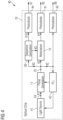
Fig. 4 shows a block diagram of an embodiment of anoptical system 40 according to the present invention. - In
Fig. 4 , the optical system is denoted byreference 40. Theoptical system 40 comprises, in particular, anintegrated circuit 10. - In addition to the embodiment example of
Fig. 3 , theintegrated circuit 10 inFig. 4 comprises alight source 41, aPLL 42 and twofurther photodiodes - The
light source 41 is an integratedoptical source 41, which can be designed, for example, as a continuous-wave laser. Thelight source 41 is directly coupled to thepulse generation unit 11 via the terminal 24 and is configured to generate the optical high frequency signal X1 for thepulse generation unit 11. - The phased-locked loop (PLL) 42 is coupled with its input side to the
output terminal 25 of thepulse generation unit 11 and with its output side to corresponding control inputs of thelight source 41 and thepulse generation unit 11. This enables the PLL to control the wavelength of the optical signal X1 generated by the integratedlight source 41 and/or to control the frequency of the pulsed wave signal X2 generated by thepulse generation unit 11, respectively. Employing thePLL 42 ensures that an exact repetition rate of the optical signal is set for use in themodulator 15 orsequence generator 30. - For synchronizing the
sequence generation unit 30 to the system clock and phase, the pulsed wave signal X2 is fed into thesequence generation unit 30. - The two
further photodiodes photodiodes photodiode 31. According to a particular preferred implementation, allphotodiodes photodiodes - One of the
photodiodes 44 is connected to thesequence generation unit 30 for receiving a trigger signal X10. Thesequence generation unit 30 generates this trigger signal X10 every time the (PRBS) sequence is started again. Thephotodiode 44 is then configured to emit a corresponding electrical trigger signal X7, which indicates when the sequence is repeated and thus provides a timing information. This trigger signal X7 may be used in an external network analyser or spectral analyser for obtaining an absolute phase reference between the control signal X3 and the electrical signal X5 and a delay information of the signals through a device under test (DUT). - The
other photodiode 43 is connected via theoutput terminal 25 to thepulse generation unit 11.Photodiode 43 is configured to emit an electrical output signal X8 based on the original optical signal X2, which indicates the original repetition rate and thus provides a clock reference. In this way, the original optical signal X2 is fed out as a clock signal, which can then be evaluated by an external device such as a spectrum analyzer or network analyser (not shown inFig. 4 ). These external devices need this clock information as a reference to know on which system clock theintegrated circuit 10 is operating. -
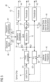
Fig. 5 shows a block diagram of a further embodiment of anoptical system 40 according to the present invention. - The
optical system 40 inFig. 5 further comprises areset unit 46 and aconfiguration unit 47 which are both coupled to acontrol interface 48 of thesequence generation unit 30. - The
configuration unit 46 is configured to generate a reset signal X11 that comprises a sequence reset information. This makes it possible to reset the setting set in thesequence generation unit 30, for example to a default setting. - The
configuration unit 47 is configured to generate a configuration signal X12 that comprises an information related to the sequence configuration. This makes it possible to set a specific operating mode with which thesequence generation unit 30 is operated, e.g. a PRBS mode, a divider mode, an arbitrary mode or any other user defined mode. - While in the embodiment in
Fig. 5 , theconfiguration unit 46 and theconfiguration unit 47 are arranged outside theintegrated circuit 10, in a preferred embodiment they may also be integrated within the integratedcircuit 10. - The
PLL 42 comprises aclock input terminal 50, which is connected to anexternal clock generator 45. Theexternal clock generator 45 is configured to provide a reference frequency X6 for thePLL 42. - The
optical system 40 also comprises aunit 49, which is connected via aninput terminal 51 to theintegrated circuit 10. Theunit 49 is configured to generate an external reference pulse signal X9 that may be provided to thephotodiode 31. This pulse signal X9 is configured such to allow diode characterization ofphotodiode 31. For this purpose, theintegrated circuit 10 comprises aswitch 52. The two input terminals of theswitch 52 are connected to theoptical modulator 15. The output terminal of theswitch 52 is connected to thephotodiode 31. In this way,photodiode 31 may be operated in a normal operation mode based on the modulated optical comb signal X4 and in diode characterization mode based on the reference pulse signal X9. -
Fig. 6 shows a block diagram of a further embodiment of anoptical system 40 according to the present invention. - A
splitter 53 is provided between theoptical modulator 15 and thephotodiode 31. Thesplitter 53 is configured to split feed the modulated optical comb signal X4 either to photodiode 31 or via anoutput terminal 54 to an externally arrangedfurther photodiode 55. This allows the modulated signal not to be led out of theintegrated circuit 10 via theintegrated photodiode 31, which is advantageous if, for example, theintegrated photodiode 31 is defective, too inaccurate or cannot be used for high-precision applications due to manufacturing tolerances. In those cases, theexternal photodiode 55 which may be optimized for the specific application can be used. - In other embodiments (not shown in the figures), for example for the same reasons a redundancy may be used for at least one of the
photodiodes photodiodes -
Fig. 7 shows a block diagram of an embodiment of a test andmeasurement device 60 according to the present invention. The test andmeasurement device 60 comprises anoptical system 40 such as the one shown inFig. 4 . The test andmeasurement device 60 can alternatively also comprise only an integrated circuit 10 (inFig. 5 shown in dotted lines) such as the one shown in any of theFigs. 1, 1A ,3 ,4 . - The test and
measurement device 50 may be a spectrum analyser, a network analyzer, an oscilloscope, a wireless communication tester or the like. The invention may also be implemented in or used for signal generators, broadband amplifiers, radio system components, etc. - In the foregoing specification, the invention has been described with reference to specific examples of embodiments of the invention. It will, however, be evident that various modifications and changes may be made therein without departing from the broader spirit and scope of the invention as set forth in the appended claims. For example, the connections between various elements as shown and described with respect to the drawings may be a type of connection suitable to transfer optical and/or electrical signals from or to the respective nodes, units or devices, for example via intermediate devices. Accordingly, unless implied or stated otherwise the connections may for example be direct connections or indirect connections.
- As the apparatuses implementing the present invention are, for the most part, composed of electronic components and circuits individually known to those skilled in the art, details of the circuitry and its components will not be explained in any greater extent than that considered necessary as illustrated above, for the understanding and appreciation of the underlying concepts of the present invention and in order not to obfuscate or distract from the teachings of the present invention.
- In the description, any reference signs shall not be construed as limiting the claim. The word "comprising" does not exclude the presence of other elements or steps then those listed in a claim. Furthermore, the terms "a" or "an", as used herein, are defined as one or more than one. Also, the use of introductory phrases such as "at least one" and "one or more" in the claims should not be construed to imply that the introduction of another claim element by the indefinite articles "a" or "an" limits any particular claim containing such introduced claim element to inventions containing only one such element, even when the same claim includes the introductory phrases "one or more" or "at least one" and indefinite articles such as "a" or "an." The same holds true for the use of definite articles. Unless stated otherwise, terms such as "first" and "second" are used to arbitrarily distinguish between the elements such terms describe. Thus, these terms are not necessarily intended to indicate temporal or other prioritization of such elements. The mere fact that certain measures are recited in mutually different claims does not indicate that a combination of these measures cannot be used to advantage.
- Skilled artisans will appreciate that the illustrations of chosen elements in the drawings are only used to help to improve the understanding of the functionality and the arrangements of these elements in various embodiments of the present invention. Also, common and well understood elements that are useful or necessary in a commercially feasible embodiment are generally not depicted in the drawings in order to facilitate the understanding of the technical concept of these various embodiments of the present invention. It will further be appreciated that certain procedural stages in the described methods may be described or depicted in a particular order of occurrence while those skilled in the art will understand that such specificity with respect to sequence is not actually required.
-
- 10
- integrated circuit
- 11
- pulse generation unit
- 12
- semiconductor substrate
- 13
- connection
- 14
- surface
- 15
- optical modulator
- 20
- Kerr-ring
- 21
- linear light guide section
- 22
- circular light guide section
- 23
- contact section
- 24
- input terminal
- 25
- output terminal
- 30
- sequence generation unit
- 31
- photodiode
- 32
- control terminal
- 40
- optical system
- 41
- light source
- 42
- PLL
- 43
- photodiode
- 44
- photodiode
- 45
- clock generator
- 46
- reset unit
- 47
- configuration unit
- 48
- control interface
- 49
- unit
- 50
- clock input terminal
- 51
- input terminal
- 52
- switch
- 53
- splitter
- 54
- output terminal
- 55
- (externally arranged) photodiode
- 60
- test and measurement device
- X1
- optical high frequency signal
- X1a
- portion of the high frequency signal
- X2
- pulsed wave signal
- X3
- modulation control signal
- X4
- modulated optical comb signal
- X5
- electrical signal
- X6
- reference frequency
- X7
- trigger signal
- X8
- output signal
- X9
- reference pulse signal
- X10
- trigger signal
- X11
- reset signal
- X12
- configuration signal
Claims (15)
- Integrated circuit, in particular photonic integrated circuit, for generating an electrical and/or optical frequency comb signal, the integrated circuit comprising:
a pulse generation unit comprising an input port for receiving an optical high frequency signal wherein the pulse generation unit comprises at least one Kerr-ring, which is arranged and configured to generate an optical comb signal from the received optical high frequency signal. - Integrated circuit according to claim 1,
further comprising an optical modulator, which is connected to the pulse generation unit for receiving the generated optical comb signal, wherein the optical modulator is configured to generate a modulated optical comb signal based on a modulation control signal. - Integrated circuit according to any of the preceding claims, wherein the material of the Kerr-ring is lithium niobate or silicon nitride.
- Integrated circuit according to any of the preceding claims, wherein at least two Kerr-rings are provided that are arranged in parallel and/or in cascade to each other.
- Integrated circuit according to any of the preceding claims, further comprising a sequence generation unit, which is configured to generate the modulation control signal for controlling the optical modulator.
- Integrated circuit according to claim 5,
wherein the sequence generation unit is configured to generate a PRBS signal that is used for controlling the modulation of the optical modulator and/or wherein sequence generation unit is configured to operate the optical modulator in a divider mode and/or an arbitrary mode. - Integrated circuit according to claim 5 or 6,
wherein the sequence generation unit is configured to generate at least one modulation control signal that causes the optical modulator to generate modulated optical comb signals having at least two different power levels and/or having at least two discrete time shifts. - Integrated circuit according to any of the claim 5 to 7, wherein the the sequence generation unit comprises at least one control input for configuring and controlling the operation of the sequence generation unit, wherein the control input is coupled to at least one of the following:- the pulse generation unit;- a reset unit;- a configuration unit;- an external terminal for receiving an externally generated control signal.
- Integrated circuit according to any of the preceding claims, further comprising at least one first photodiode, in particular a broadband photodiode, for generating an electrical comb signal from the modulated optical comb signal.
- Integrated circuit according to any of the preceding claims,
further comprising at least one optical splitter and an optical output terminal connected to the optical splitter, wherein the optical splitter is configured to split the modulated optical comb signal and to feed the split modulated optical comb signal to the first photodiode and/or the optical output terminal. - Integrated circuit according to any of the preceding claims,
further comprising at least one of:- at least one further optical modulator connected to the pulse generation unit for receiving the generated optical comb signal;- at least one second photodiode connected to the sequence generation unit, wherein the sequence generation unit is configured to generate a timing trigger signal for the second photodiode;at least one third photodiode directly connected to the output terminal of the pulse generation unit. - Integrated circuit according to any of the preceding claims,
further comprising a phased-locked loop circuit, which is configured to control the frequency of the pulse generation unit and/or the repetition rate generated by the integrated laser. - Integrated circuit according to any of the preceding claims,
further comprising an external optical input port for receiving an external optical signal and a switching unit, wherein in a first switching mode the switching unit is configured to connect the optical modulator to a first photodiode, and in a second switching mode the switching unit is configured to connect the external optical input port to the first photodiode. - Optical system, the optical system comprising:at least one integrated circuit according to any of the preceding claims; andat least one optical component, which is connected to the integrated circuit via an optical or electrical interface, wherein the at least one optical component comprises at least one of the following:- an external laser connected via an optical input terminal to the pulse generation unit of the integrated circuit, which is configured to generate an optical high frequency signal;- at least one external photodiode connected via an optical output terminal to the integrated circuit.
- Test and measurement device comprising the integrated circuit according to any of the claims 1 to 13 and/or the optical system according to claim 14.
Priority Applications (3)
| Application Number | Priority Date | Filing Date | Title |
|---|---|---|---|
| EP23163326.4A EP4435508A1 (en) | 2023-03-22 | 2023-03-22 | Integrated circuit for generating a frequency comb signal, optical system and test and measurement device |
| US18/586,855 US20240319561A1 (en) | 2023-03-22 | 2024-02-26 | Integrated circuit for generating a frequency comb signal, optical system and test and measurement device |
| CN202410320423.5A CN118689015A (en) | 2023-03-22 | 2024-03-20 | Integrated circuit, optical system and test and measurement device for generating frequency comb signals |
Applications Claiming Priority (1)
| Application Number | Priority Date | Filing Date | Title |
|---|---|---|---|
| EP23163326.4A EP4435508A1 (en) | 2023-03-22 | 2023-03-22 | Integrated circuit for generating a frequency comb signal, optical system and test and measurement device |
Publications (1)
| Publication Number | Publication Date |
|---|---|
| EP4435508A1 true EP4435508A1 (en) | 2024-09-25 |
Family
ID=85726623
Family Applications (1)
| Application Number | Title | Priority Date | Filing Date |
|---|---|---|---|
| EP23163326.4A Pending EP4435508A1 (en) | 2023-03-22 | 2023-03-22 | Integrated circuit for generating a frequency comb signal, optical system and test and measurement device |
Country Status (3)
| Country | Link |
|---|---|
| US (1) | US20240319561A1 (en) |
| EP (1) | EP4435508A1 (en) |
| CN (1) | CN118689015A (en) |
Citations (6)
| Publication number | Priority date | Publication date | Assignee | Title |
|---|---|---|---|---|
| US20180083414A1 (en) * | 2014-02-24 | 2018-03-22 | Purdue Research Foundation | Mode-locked and wavelength tunable optical frequency comb generation through dynamic control of microresonators |
| CN110168444A (en) * | 2016-10-31 | 2019-08-23 | 加利福尼亚大学董事会 | The frequency comb for being insulated dispersion management generates |
| US20190312402A1 (en) * | 2018-04-10 | 2019-10-10 | Ecole Polytechnique Federale De Lausanne (Epfl) | Multiple soliton comb generation method and device |
| US10707968B2 (en) | 2018-09-19 | 2020-07-07 | Rohde & Schwarz Gmbh & Co. Kg | Frequency comb generating device and method for generating a frequency comb |
| US20210096444A1 (en) * | 2018-04-30 | 2021-04-01 | President And Fellows Of Harvard College | Optical frequency comb generation in integrated lithium niobate devices |
| US20210242654A1 (en) * | 2020-02-03 | 2021-08-05 | Yale University | Octave-Spanning Soliton Comb |
Family Cites Families (1)
| Publication number | Priority date | Publication date | Assignee | Title |
|---|---|---|---|---|
| CN111796469B (en) * | 2019-04-09 | 2022-08-19 | 华为技术有限公司 | Optical frequency comb light source and method for generating optical frequency comb |
-
2023
- 2023-03-22 EP EP23163326.4A patent/EP4435508A1/en active Pending
-
2024
- 2024-02-26 US US18/586,855 patent/US20240319561A1/en active Pending
- 2024-03-20 CN CN202410320423.5A patent/CN118689015A/en active Pending
Patent Citations (6)
| Publication number | Priority date | Publication date | Assignee | Title |
|---|---|---|---|---|
| US20180083414A1 (en) * | 2014-02-24 | 2018-03-22 | Purdue Research Foundation | Mode-locked and wavelength tunable optical frequency comb generation through dynamic control of microresonators |
| CN110168444A (en) * | 2016-10-31 | 2019-08-23 | 加利福尼亚大学董事会 | The frequency comb for being insulated dispersion management generates |
| US20190312402A1 (en) * | 2018-04-10 | 2019-10-10 | Ecole Polytechnique Federale De Lausanne (Epfl) | Multiple soliton comb generation method and device |
| US20210096444A1 (en) * | 2018-04-30 | 2021-04-01 | President And Fellows Of Harvard College | Optical frequency comb generation in integrated lithium niobate devices |
| US10707968B2 (en) | 2018-09-19 | 2020-07-07 | Rohde & Schwarz Gmbh & Co. Kg | Frequency comb generating device and method for generating a frequency comb |
| US20210242654A1 (en) * | 2020-02-03 | 2021-08-05 | Yale University | Octave-Spanning Soliton Comb |
Non-Patent Citations (1)
| Title |
|---|
| JIAYANG WU ET AL: "Harnessing optical micro-combs for microwave photonics", ARXIV.ORG, CORNELL UNIVERSITY LIBRARY, 201 OLIN LIBRARY CORNELL UNIVERSITY ITHACA, NY 14853, 24 October 2017 (2017-10-24), XP081313398, DOI: 10.1109/JSTQE.2018.2805814 * |
Also Published As
| Publication number | Publication date |
|---|---|
| US20240319561A1 (en) | 2024-09-26 |
| CN118689015A (en) | 2024-09-24 |
Similar Documents
| Publication | Publication Date | Title |
|---|---|---|
| Liu et al. | Microwave pulse generation with a silicon dual-parallel modulator | |
| US6819475B2 (en) | Optical frequency converter | |
| CN115754922A (en) | Ultra-wideband multi-channel beam forming method based on Kerr optical frequency comb and network system | |
| US5870211A (en) | Error rate measurement system for high speed optical pulse signals | |
| Bai et al. | Microwave photonic links and transversal microwave photonic applications | |
| Hao et al. | Simultaneous dual-band frequency-agile microwave signal generation with a dual loop Fourier domain mode locked optoelectronic oscillator | |
| US20240319561A1 (en) | Integrated circuit for generating a frequency comb signal, optical system and test and measurement device | |
| Deakin et al. | 2.4-thz bandwidth optical coherent receiver based on a photonic crystal microcomb | |
| US6541951B2 (en) | Optical measurement of target-light waveform | |
| CA2700345A1 (en) | Highly tunable, low jitter optical clock generation | |
| WO2020226728A2 (en) | Radio frequency to optical transmitter | |
| Hauenschild et al. | Demonstration of retiming capability of silicon bipolar time-division multiplexer operating to 24 Gbit/s | |
| CN117014073A (en) | Direct spread spectrum frequency hopping hybrid communication device and method based on single optical frequency comb | |
| CN115912025A (en) | Multi-band reconfigurable Fourier mode-locked optoelectronic oscillator | |
| Rzaigui et al. | Optical heterodyning for reduction of chromatic dispersion sensitivity in 60 GHz mode-locked laser systems | |
| US10200128B1 (en) | RF generation using tunable optical source | |
| Zhang et al. | Chip-Based Widely Tunable and Independently Switchable Multiple Narrow Bandpass Microwave Photonic Filters | |
| Capmany | Microwave photonic filters | |
| RU2845187C1 (en) | Device for quantum distribution of cryptographic key with frequency coding | |
| Deakin | Dual optical frequency comb analog to digital conversion | |
| JP3449019B2 (en) | Optical multiplexing equipment | |
| CN118472788B (en) | Multipath broadband white noise generation method based on chaotic micro-ring optical frequency comb | |
| Ismaeel et al. | A Comprehensive Survey on Microwave Photonic Filter: Design Techniques and Implementations | |
| Abu-Elmaaty et al. | M-PPM Fast Delay Unit Based on Silicon-on-Insulator Coupled Resonator Optical Waveguides | |
| JP2025154648A (en) | Transmitter and transmission method |
Legal Events
| Date | Code | Title | Description |
|---|---|---|---|
| PUAI | Public reference made under article 153(3) epc to a published international application that has entered the european phase |
Free format text: ORIGINAL CODE: 0009012 |
|
| STAA | Information on the status of an ep patent application or granted ep patent |
Free format text: STATUS: THE APPLICATION HAS BEEN PUBLISHED |
|
| AK | Designated contracting states |
Kind code of ref document: A1 Designated state(s): AL AT BE BG CH CY CZ DE DK EE ES FI FR GB GR HR HU IE IS IT LI LT LU LV MC ME MK MT NL NO PL PT RO RS SE SI SK SM TR |
|
| STAA | Information on the status of an ep patent application or granted ep patent |
Free format text: STATUS: REQUEST FOR EXAMINATION WAS MADE |
|
| 17P | Request for examination filed |
Effective date: 20250226 |