EP4435448A1 - High-side driver diagnosis method and battery system - Google Patents
High-side driver diagnosis method and battery system Download PDFInfo
- Publication number
- EP4435448A1 EP4435448A1 EP24164585.2A EP24164585A EP4435448A1 EP 4435448 A1 EP4435448 A1 EP 4435448A1 EP 24164585 A EP24164585 A EP 24164585A EP 4435448 A1 EP4435448 A1 EP 4435448A1
- Authority
- EP
- European Patent Office
- Prior art keywords
- relay
- voltage
- switching element
- relays
- hsd
- Prior art date
- Legal status (The legal status is an assumption and is not a legal conclusion. Google has not performed a legal analysis and makes no representation as to the accuracy of the status listed.)
- Pending
Links
Images



Classifications
-
- G—PHYSICS
- G01—MEASURING; TESTING
- G01R—MEASURING ELECTRIC VARIABLES; MEASURING MAGNETIC VARIABLES
- G01R31/00—Arrangements for testing electric properties; Arrangements for locating electric faults; Arrangements for electrical testing characterised by what is being tested not provided for elsewhere
- G01R31/327—Testing of circuit interrupters, switches or circuit-breakers
- G01R31/3277—Testing of circuit interrupters, switches or circuit-breakers of low voltage devices, e.g. domestic or industrial devices, such as motor protections, relays, rotation switches
- G01R31/3278—Testing of circuit interrupters, switches or circuit-breakers of low voltage devices, e.g. domestic or industrial devices, such as motor protections, relays, rotation switches of relays, solenoids or reed switches
-
- G—PHYSICS
- G01—MEASURING; TESTING
- G01R—MEASURING ELECTRIC VARIABLES; MEASURING MAGNETIC VARIABLES
- G01R31/00—Arrangements for testing electric properties; Arrangements for locating electric faults; Arrangements for electrical testing characterised by what is being tested not provided for elsewhere
- G01R31/50—Testing of electric apparatus, lines, cables or components for short-circuits, continuity, leakage current or incorrect line connections
- G01R31/52—Testing for short-circuits, leakage current or ground faults
-
- G—PHYSICS
- G01—MEASURING; TESTING
- G01R—MEASURING ELECTRIC VARIABLES; MEASURING MAGNETIC VARIABLES
- G01R31/00—Arrangements for testing electric properties; Arrangements for locating electric faults; Arrangements for electrical testing characterised by what is being tested not provided for elsewhere
- G01R31/40—Testing power supplies
-
- G—PHYSICS
- G01—MEASURING; TESTING
- G01R—MEASURING ELECTRIC VARIABLES; MEASURING MAGNETIC VARIABLES
- G01R31/00—Arrangements for testing electric properties; Arrangements for locating electric faults; Arrangements for electrical testing characterised by what is being tested not provided for elsewhere
- G01R31/36—Arrangements for testing, measuring or monitoring the electrical condition of accumulators or electric batteries, e.g. capacity or state of charge [SoC]
-
- G—PHYSICS
- G01—MEASURING; TESTING
- G01R—MEASURING ELECTRIC VARIABLES; MEASURING MAGNETIC VARIABLES
- G01R19/00—Arrangements for measuring currents or voltages or for indicating presence or sign thereof
- G01R19/0038—Circuits for comparing several input signals and for indicating the result of this comparison, e.g. equal, different, greater, smaller (comparing pulses or pulse trains according to amplitude)
-
- G—PHYSICS
- G01—MEASURING; TESTING
- G01R—MEASURING ELECTRIC VARIABLES; MEASURING MAGNETIC VARIABLES
- G01R31/00—Arrangements for testing electric properties; Arrangements for locating electric faults; Arrangements for electrical testing characterised by what is being tested not provided for elsewhere
- G01R31/327—Testing of circuit interrupters, switches or circuit-breakers
- G01R31/3271—Testing of circuit interrupters, switches or circuit-breakers of high voltage or medium voltage devices
- G01R31/3272—Apparatus, systems or circuits therefor
- G01R31/3274—Details related to measuring, e.g. sensing, displaying or computing; Measuring of variables related to the contact pieces, e.g. wear, position or resistance
-
- G—PHYSICS
- G01—MEASURING; TESTING
- G01R—MEASURING ELECTRIC VARIABLES; MEASURING MAGNETIC VARIABLES
- G01R31/00—Arrangements for testing electric properties; Arrangements for locating electric faults; Arrangements for electrical testing characterised by what is being tested not provided for elsewhere
- G01R31/327—Testing of circuit interrupters, switches or circuit-breakers
- G01R31/3271—Testing of circuit interrupters, switches or circuit-breakers of high voltage or medium voltage devices
- G01R31/3275—Fault detection or status indication
-
- G—PHYSICS
- G01—MEASURING; TESTING
- G01R—MEASURING ELECTRIC VARIABLES; MEASURING MAGNETIC VARIABLES
- G01R31/00—Arrangements for testing electric properties; Arrangements for locating electric faults; Arrangements for electrical testing characterised by what is being tested not provided for elsewhere
- G01R31/50—Testing of electric apparatus, lines, cables or components for short-circuits, continuity, leakage current or incorrect line connections
- G01R31/56—Testing of electric apparatus
-
- H—ELECTRICITY
- H01—ELECTRIC ELEMENTS
- H01M—PROCESSES OR MEANS, e.g. BATTERIES, FOR THE DIRECT CONVERSION OF CHEMICAL ENERGY INTO ELECTRICAL ENERGY
- H01M10/00—Secondary cells; Manufacture thereof
- H01M10/42—Methods or arrangements for servicing or maintenance of secondary cells or secondary half-cells
- H01M10/425—Structural combination with electronic components, e.g. electronic circuits integrated to the outside of the casing
-
- H—ELECTRICITY
- H03—ELECTRONIC CIRCUITRY
- H03K—PULSE TECHNIQUE
- H03K17/00—Electronic switching or gating, i.e. not by contact-making and –breaking
- H03K17/51—Electronic switching or gating, i.e. not by contact-making and –breaking characterised by the components used
- H03K17/56—Electronic switching or gating, i.e. not by contact-making and –breaking characterised by the components used by the use, as active elements, of semiconductor devices
- H03K17/687—Electronic switching or gating, i.e. not by contact-making and –breaking characterised by the components used by the use, as active elements, of semiconductor devices the devices being field-effect transistors
- H03K17/6871—Electronic switching or gating, i.e. not by contact-making and –breaking characterised by the components used by the use, as active elements, of semiconductor devices the devices being field-effect transistors the output circuit comprising more than one controlled field-effect transistor
-
- H—ELECTRICITY
- H01—ELECTRIC ELEMENTS
- H01M—PROCESSES OR MEANS, e.g. BATTERIES, FOR THE DIRECT CONVERSION OF CHEMICAL ENERGY INTO ELECTRICAL ENERGY
- H01M10/00—Secondary cells; Manufacture thereof
- H01M10/42—Methods or arrangements for servicing or maintenance of secondary cells or secondary half-cells
- H01M10/425—Structural combination with electronic components, e.g. electronic circuits integrated to the outside of the casing
- H01M2010/4271—Battery management systems including electronic circuits, e.g. control of current or voltage to keep battery in healthy state, cell balancing
Definitions
- the present disclosure relates to a diagnosis method and a battery system.
- a mechanical relay may be used for opening and closing a high voltage battery output in a battery pack.
- the mechanical relay may be formed to include a coil stage and a high current stage, and if a current that is greater than a trip current flows through the coil, a magnetic force is generated to connect opposite terminals of the high current stage to allow a current to flow therethrough.
- the coil stage may include a large inductive reactance and a low resistance to allow a sufficient excitation current to flow to the coil, and the high-current stage may include a very small resistance to reduce power consumption and heat generation.
- a driver that drives such a relay may include a plurality of high-side drivers (HSDs) for driving a plurality of high-side switches between a plurality of relays and a relay driving power supply, and may include a low-side driver (LSD) for driving the low-side switches between the relays and a ground.
- HSDs high-side drivers
- LSD low-side driver
- Various failures may occur in an HSD, a LSD, a relay, a battery, etc. A technique for detecting these failures may be desirable.
- the present disclosure provides a diagnosis method for a high-side driver and a battery system that are capable of detecting a short circuit between a plurality of pins (hereinafter referred to as a pin-to-pin short circuit) that are for applying signals to drive a plurality of high-side switches.
- One or more embodiments of the present disclosure provide a battery system including a battery pack, relays connected to the battery pack, a high-side driver (HSD) configured to apply a relay driving voltage to high-sides of the relays, and a battery management system (BMS) configured to diagnose the HSD based on a voltage measured from first ends of the relays or the HSD.
- HSD high-side driver
- BMS battery management system
- the battery system may further include a low-side driver (LSD) configured to connect a first node, which is connected to low-sides of the relays, and a ground (e.g., the LSD may be connected between low-sides of the relays and a ground).
- LSD low-side driver
- the battery system may further include voltage sensors configured to generate voltage measurement signals, wherein the BMS may include a main control unit (MCU) configured to drive the HSD to supply a voltage (e.g., the relay driving voltage) to relay coils corresponding to the relays, and a diagnostic device configured to diagnose the HSD based on the voltage measurement signals.
- MCU main control unit
- the voltage sensors may be configured to measure high-side voltages of the relays (e.g., voltages from first ends of the relays), wherein the HSD may include first switching elements configured to apply the relay driving voltage to the relays.
- the battery system may further include blocking elements including a diode having an anode connected to a low-side of a corresponding one of the relays, and having a cathode connected to the first node.
- the MCU may be further configured to output driving signals (e.g., high-side driving signals) for the first switching elements to the HSD, wherein the HSD may further include drivers for outputting inverted driving signals obtained by inverting the driving signals (e.g., high-side driving signals) for the first switching elements.
- driving signals e.g., high-side driving signals
- the HSD may further include drivers for outputting inverted driving signals obtained by inverting the driving signals (e.g., high-side driving signals) for the first switching elements.
- the battery system may further include blocking elements including a second switching element including a drain connected to a low-side of a corresponding one of the relays, a source connected to the first node, and a gate for receiving a corresponding one of the inverted driving signals from a corresponding one of the drivers, and a diode having an anode connected to the drain, and a cathode connected to the source.
- blocking elements including a second switching element including a drain connected to a low-side of a corresponding one of the relays, a source connected to the first node, and a gate for receiving a corresponding one of the inverted driving signals from a corresponding one of the drivers, and a diode having an anode connected to the drain, and a cathode connected to the source.
- the voltage sensors may be configured to respectively measure voltages of the relays (e.g., corresponding voltages of the HSD), wherein the MCU may be further configured to generate high-side driving signals corresponding to the relays to transmit them to the HSD, and wherein the HSD may include elements (e.g., "ideal elements") configured to apply the relay driving voltage to the relays, and drivers configured to receive the high-side driving signals from pins to drive the elements.
- elements e.g., "ideal elements”
- the elements may include a first switching element configured to have a drain to which the relay driving voltage is applied, a second switching element configured to have a source connected to a source of the first switching element, and a drain connected to a high-side of one of the relays, a first diode configured to have an anode connected to the source of the first switching element, and a cathode connected to the drain of the first switching element, and a second diode configured to have an anode connected to the source of the second switching element, and a cathode connected to the drain of the second switching element, and wherein the drivers may be further configured to respectively supply voltages (e.g., gate signals) to gates of the first switching elements and to gates of the second switching elements.
- voltages e.g., gate signals
- One of the voltage sensors may be further configured to generate one of the voltage measurement signals by measuring a voltage from a node to which the source of the first switching element and the source of the second switching element is connected, and to transmit the one of the voltage measurement signals to the diagnostic device.
- One or more embodiments of the present disclosure provide a diagnosis method including applying a relay driving voltage to high-sides of relays connected to a battery pack, obtaining voltage signals (e.g., voltage measurement signals) by measuring a voltage from first ends of the relays (e.g., high-side voltages of the relays) or a high-side driver (HSD), and diagnosing the HSD based on the voltage signals.
- voltage signals e.g., voltage measurement signals
- HSD high-side driver
- the diagnosis method may further include connecting a first node, which is connected to low-sides of the relays, and a ground.
- the diagnosis method may further include driving the HSD to supply a voltage (e.g., the relay driving voltage) to relay coils corresponding to the relays.
- a voltage e.g., the relay driving voltage
- the applying of the relay driving voltage may include applying a driving signal (e.g., a high-side driving signal) to a first switching element connected to a high-side of one of the relays, wherein the first switching element may include a gate to which the driving signal (e.g., the high-side driving signal) is applied, a drain to which the relay driving voltage is applied, and a source connected to a high-side of a corresponding relay of the relays, and wherein the first switching element may be configured to transmit the relay driving voltage to the high-side of the corresponding relay based on the driving signal (e.g., the high-side driving signal).
- a driving signal e.g., a high-side driving signal
- the applying of the relay driving voltage may further include applying an inverted driving signal, in which the driving signal (e.g., the high-side driving signal) applied to the first switching element connected to the corresponding relay is inverted, to a blocking element connected to a corresponding low-side of the low-sides of the corresponding relay, wherein the blocking element may be connected between the corresponding relay and the first node, respectively, and may include a second switching element, wherein the second switching element may include a gate for receiving the inverted driving signal, a drain connected to the corresponding low-side, and a source connected to the first node, and wherein the second switching element connects the corresponding low-side to the first node based on the inverted driving signal.
- the driving signal e.g., the high-side driving signal
- the applying of the relay driving voltage may include receiving a high-side driving signal corresponding to a corresponding relay of the relays from a battery management system (BMS), and driving an element (e.g., an "ideal element") to apply the relay driving voltage to the corresponding relay.
- BMS battery management system
- the element may include a first switching element including a drain for receiving the relay driving voltage, and a second switching element including a source connected to a source of the first switching element, and a drain connected to a high-side of the corresponding relay, and wherein the driving of the element (e.g., the "ideal element") may include supplying a voltage (e.g., a gate signal) to a gate of the first switching element and to a gate of the second switching element.
- a voltage e.g., a gate signal
- the measuring of the voltage may include generating a voltage measurement signal by measuring a voltage from a node to which the source of the first switching element and the source of the second switching element of the element are connected, and transmitting the voltage measurement signal to the BMS.
- reliability of diagnosis may be secured through low-side common operation of the plurality of relays, and not only may complex interfaces be simplified, and high costs may be reduced, but also fault diagnosis of HSD is possible.
- an automotive safety integrity level may be improved according to reduction of failures in time (FIT) by broadening a diagnostic area of the battery system.
- a layer, region, or component when referred to as being “electrically connected” or “electrically coupled” to another layer, region, or component, it can be directly electrically connected or coupled to the other layer, region, and/or component or intervening layers, regions, or components may be present.
- directly connected/directly coupled refers to one component directly connecting or coupling another component without an intermediate component.
- expressions such as "at least one of,” or “any one of,” or “one or more of” when preceding a list of elements, modify the entire list of elements and do not modify the individual elements of the list.
- “at least one of X, Y, and Z,” “at least one of X, Y, or Z,” “at least one selected from the group consisting of X, Y, and Z,” and “at least one selected from the group consisting of X, Y, or Z” may be construed as X only, Y only, Z only, any combination of two or more of X, Y, and Z, such as, for instance, XYZ, XYY, YZ, and ZZ, or any variation thereof.
- the expression, such as “at least one of A and B” and “at least one of A or B” may include A, B, or A and B.
- “or” generally means “and/or,” and the term “and/or” includes any and all combinations of one or more of the associated listed items.
- the expression, such as “A and/or B” may include A, B, or A and B.
- first,” “second,” “third,” etc. may be used herein to describe various elements, components, regions, layers and/or sections, these elements, components, regions, layers and/or sections should not be limited by these terms. These terms do not correspond to a particular order, position, or superiority, and are used only used to distinguish one element, member, component, region, area, layer, section, or portion from another element, member, component, region, area, layer, section, or portion. Thus, a first element, component, region, layer or section described below could be termed a second element, component, region, layer or section, without departing from the scope of the present disclosure.
- first element may not require or imply the presence of a second element or other elements.
- first,” second,” etc. may also be used herein to differentiate different categories or sets of elements.
- first, second, etc. may represent “first-category (or first-set),” “second-category (or secondset),” etc., respectively.
- a specific process order may be performed differently from the described order.
- two consecutively described processes may be performed substantially at the same time or performed in an order opposite to the described order.
- the term “substantially,” “about,” “approximately,” and similar terms are used as terms of approximation and not as terms of degree, and are intended to account for the inherent deviations in measured or calculated values that would be recognized by those of ordinary skill in the art.
- “About” or “approximately,” as used herein, is inclusive of the stated value and means within an acceptable range of deviation for the particular value as determined by one of ordinary skill in the art, considering the measurement in question and the error associated with measurement of the particular quantity (i.e., the limitations of the measurement system). For example, “about” may mean within one or more standard deviations, or within ⁇ 30%, 20%, 10%, 5% of the stated value. Further, the use of “may” when describing embodiments of the present disclosure refers to "one or more embodiments of the present disclosure.”
- each block, unit, and/or module may be implemented by dedicated hardware, or a combination of dedicated hardware that performs some functions and a processor (for example, one or more programmed microprocessors and related circuits) that performs a function different from those of the dedicated hardware.
- the block, unit, and/or module may be physically separated into two or more interact individual blocks, units, and/or modules without departing from the scope of the present disclosure.
- the block, unit and/or module may be physically combined into more complex blocks, units, and/or modules without departing from the scope of the present disclosure.
- a program implemented as a set of commands embodying a control algorithm suitable for controlling a second element may be installed in a first element for controlling the second element under a specific control condition among elements according to one or more embodiments.
- a control element may process input data and stored data depending on an installed program to generate output data.
- the control element may include a non-volatile memory to store a program and a memory to store data.
- FIG. 1 illustrates a block diagram schematically showing a battery system according to one or more embodiments of the present disclosure.
- the battery system 1 may include a battery pack 100, a relay bank (e.g., relay unit) 200, a relay driver 300, and a battery management system (BMS) 400.
- a relay bank e.g., relay unit
- BMS battery management system
- An external device 2 may include a load, such as an inverter or a converter and/or a charging device.
- a load such as an inverter or a converter
- opposite ends P+ and P- of the battery system 1 may be connected to a charger to receive power from the charger and may be charged.
- both ends P+ and P- of the battery system 1 may be connected to a load to allow a power supplied by the battery pack 100 to be discharged through the load.
- the battery pack 100 may include a plurality of battery cells connected in series and/or in parallel.
- the relay bank 200 may include a plurality of relays connected to the battery pack 100. A first end of the relay bank 200 may be connected to the battery pack 100, and a second end of the relay bank 200 may be connected to one of opposite ends of the battery system 1.
- the relay bank 200 may include a plurality of relays among at least one first relay connected between a first end (+ terminal) of the battery pack 100 and a first end (P+) of the battery system 1, and may include at least one second relay connected between the other end (- terminal) of the battery pack 100 and a second end (P-) of the battery system 1.
- a number of relays included in the relay bank 200 will be described as plural.
- the relay driver 300 may drive the relay bank 200 under control of the BMS 400.
- the relay driver 300 may include a plurality of high-side drivers (HSDs) and low-side drivers (LSDs).
- HSDs high-side drivers
- LSDs low-side drivers
- the HSDs may drive a high-side switch between a plurality of relays included in the relay driver 300 and a relay driving voltage for driving the relays.
- the LSDs may drive a low-side switch between the multiple relays and a ground.
- the relay driver 300 may drive each of the relays included in the relay bank 200 at a high-side of each of the relays while commonly operating a low-side of the relay bank 200.
- the relay driver 300 may include a blocking element in a high-side channel corresponding to each of the relays.
- the relay driver 300 enables independent diagnosis of the HSDs corresponding to the relays by blocking a voltage and/or a current through a blocking element corresponding to the remaining relays with the exception of one relay to be monitored among the relays.
- the BMS 400 may control an operation of the relay driver 300, and may diagnose a plurality of HSDs.
- the BMS 400 may control an operation of the relay driver 300, including, for example, a plurality of HSDs, LSDs, and blocking elements.
- the BMS 400 also may monitor a voltage and/or a current in the relay bank 200 and/or the relay driver 300.
- the BMS 400 also may diagnose the relay driver 300 based on a measured voltage.
- the BMS 400 may measure voltages from first ends of the relays included in the relay bank 200, and may measure currents from wires included in the relay driver 300.
- the BMS 400 may diagnose a state of the HSDs included in the relay driver 300 by diagnosing the relay driver 300.
- FIG. 2 illustrates a block diagram schematically showing a detailed configuration of the battery system of FIG. 1 .
- the battery system 11 illustrated in FIG. 2 is an example of the battery system 1 of FIG. 1 .
- descriptions of overlapping portions with those of the battery system 1 may be omitted.
- the battery system 11 may include a battery pack 100, a relay bank 200, a relay driver 300, and a BMS 400.
- the relay bank 200 may include a plurality of relays 210, 220, 230, and 240, a plurality of voltage sensors 410, 420, 430, and 440, and a plurality of blocking elements 510, 520, 530, and 540.
- the present disclosure is not limited thereto, and in some embodiments, the voltage sensors 410, 420, 430, and 440 may be included in the HSD 310, or may be distinguished from the HSD 310 and the relay 220.
- the voltage sensors 410, 420, 430, and 440 may respectively measure voltages from first ends of the relays 210, 220, 230, and 240.
- the relay driver 300 may include an HSD 310 and an LSD 320.
- the BMS 400 may include a main control unit (MCU) 401 and a diagnostic device (e.g., a diagnosis unit) 402.
- the external device 2 may include a capacitor C1 and a capacitor C2.
- the relay 210 may be a positive pre-charge relay. A first end of the relay 210 may be connected to a positive terminal (+) of the battery pack 100, and a second end of the relay 210 may be connected to a first end of the capacitor C2.
- the relay 210 may include a relay coil 211.
- the relay 220 may be a positive main relay. A first end of the relay 220 may be connected to a positive terminal (+) of the battery pack 100, and a second end of the relay 220 may be connected to a first end of the capacitor C1.
- the relay 220 may include a relay coil 221.
- the relay 230 may be a negative main relay. A first end of the relay 230 may be connected to a negative terminal (-) of the battery pack 100, and a second end of the relay 230 may be connected to a second end of the capacitor C1.
- the relay 230 may include a relay coil 231.
- the relay 240 may be a negative pre-charge relay. A first end of the relay 240 may be connected to a negative terminal (-) of the battery pack 100, and a second end of the relay 240 may be connected to a second end of the capacitor C2.
- the relay 240 may include a relay coil 241.
- the HSD 310 may supply relay coil voltages to the relay coils 211, 221, 231, and 241.
- the HSD 310 may include a plurality of terminals P11, P12, P13, and P14. Each of the terminals P11, P12, P13, and P14 may correspond to a pin of the HSD 310.
- a low voltage power source LV may be supplied to the HSD 310.
- the low voltage power source LV may be an auxiliary voltage of a vehicle.
- the MCU 401 may generate and transmit a plurality of high-side driving signals HSD1_EN, HSD2_EN, HSD3_EN, and HSD4_EN to the HSD 310.
- the MCU 401 may drive the HSD 310 to supply a voltage to each of the relay coils 211, 221, 231, and 241.
- the HSD 310 may supply a relay coil voltage to a high-side (first end) of each of the relay coils 211, 221, 231, and 241 through the terminals P11, P12, P13, and P14 according to multiple high-side driving signals HSD1_EN, HSD2_EN, HSD3_EN, and HSD4_EN. For example, upon receiving an on-level high-side driving signal HSD1_EN from the MCU 401, the HSD 310 may apply an on-level relay coil voltage to a high-side of the relay coil 211 through the terminal P11.
- a corresponding relay among the relays 210, 220, 230, and 240 may be turned on by a magnetic field caused by a current flowing in the relay coil (e.g., relay coil 211) to which an on-level relay coil voltage is applied among the relay coils 211, 221, 231, and 241.
- the relay e.g., relay 210 to be turned on by the MCU 401 through the high-side driving signals HSD1_EN, HSD2_EN, HSD3_EN, and HSD4_EN is referred to as a target relay.
- Each of a plurality of blocking elements 510, 520, 530, and 540 may be connected to a second end of a corresponding relay coil (e.g., relay coil 211) among the relay coils 211, 221, 231, and 241.
- the blocking elements 510, 520, 530, and 540 may block a voltage supplied to relays other than the target relay among the relays 210, 220, 230, and 240.
- each of the blocking elements 510, 520, 530, and 540 is shown as being connected to a second end of a corresponding relay coil among the plurality of relay coils 211, 221, 231, and 241, but the present disclosure is not limited thereto.
- each of the blocking elements 510, 520, 530, and 540 may be included in the HSD 310 to block a voltage supplied to the remaining relays excluding the target relay among the relays 210, 220, 230, and 240.
- numbers of the relays 210, 220, 230, 240, of the blocking elements 510, 520, 530, and 540 respectively corresponding to the relays 210, 220, 230, and 240, and of voltage sensors 410, 420, 430, and 440 each were illustrated as four, but this is for convenience of description, and the present disclosure is not limited thereto.
- the battery system 11 may include a plurality of relays, a plurality of blocking elements, and a plurality of voltage sensors.
- a number of the blocking elements may correspond to the number of the relays
- a number of the voltage sensors may also correspond to the number of relays. For example, if there are 4 relays, the battery system 11 may also include 4 blocking elements and 4 voltage sensors.
- the MCU 401 may generate and transmit a low-side driving signal LSD_EN to an LSD 320.
- the LSD 320 may connect low-sides of the relay coils 211, 221, 231, and 241 to the ground according to the low-side driving signal LSD_EN.
- a first end (high-side) of each of the relay coils 211, 221, 231, and 241 is connected to the HSD 310, and a second end (low-side) of each of the relay coils 211, 221, 231, and 241 may be connected to the LSD 320.
- a corresponding voltage sensor (e.g., voltage sensor 410) may be provided at a first end of each of the relay coils 211, 221, 231, and 241 (e.g., relay coil 211).
- the voltage sensor 410 may generate a voltage measurement signal VS1 by measuring a voltage of the relay coil 211 at a first end.
- the voltage sensor 420 may generate a voltage measurement signal VS2 by measuring a voltage of the relay coil 221 at a first end.
- the voltage sensor 430 may generate a voltage measurement signal VS3 by measuring a voltage of the relay coil 231 at a first end.
- the voltage sensor 440 may generate a voltage measurement signal VS4 by measuring a voltage of the relay coil 241 at a first end.
- the voltage sensors 410, 420, 430, and 440 may respectively transmit the generated voltage measurement signals VS1, VS2, VS3, and VS4 to the diagnostic device 402.
- the diagnostic device 402 may diagnose the HSD 310 and/or the relays 210, 220, 230, and 240 based on the plurality of voltage measurement signals VS1, VS2, VS3, and VS4.
- each of the voltage sensors 410, 420, 430, and 440 is illustrated as only connecting to the first end of the relays 210, 220, 230, and 240, but this is for convenience of description, and the present disclosure is not limited thereto.
- a voltage sensor may be connected to each of high and low-sides of the relays 210, 220, 230, and 240.
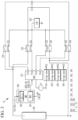
- FIG. 3 illustrates an example circuit diagram if a blocking element included in the battery system of FIG. 2 includes a diode.
- the relay bank 200 and the relay driver 300 of FIG. 2 may include a plurality of relays 210, 220, 230, and 240, an HSD 310_1, an LSD 320, and a plurality of voltage sensors 410, 420, 430, 440, and 450, and a plurality of blocking elements 510_1, 520_1, 530_1, and 540_1.
- a high-side (first end) of the relay 210 is called a node N_HS1
- a high-side (first end) of the relay 220 is called a node N_HS2
- a high-side (first end) of the relay 230 is called a node N_HS3
- a high-side (first end) of the relay 240 is referred to as a node N_HS4.
- a low-side (second end) of each of the relays 210, 220, 230, and 240 is referred to as a node N_LS.
- the relay 210 may include a relay coil 211 and a resistor R1.
- the relay 220 may include a relay coil 221 and a resistor R2.
- the relay 230 may include a relay coil 231 and a resistor R3.
- the relay 240 may include a relay coil 241 and a resistor R4.
- the HSD 310_1 may include a plurality of switching elements M1, M2, M3, and M4.
- the switching elements M1, M2, M3, and M4 may be N-channel metal-oxide-semiconductor field effect transistors (MOSFETs).
- MOSFETs metal-oxide-semiconductor field effect transistors
- the switching elements M1, M2, M3, and M4 may correspond to the relays 210, 220, 230, and 240.
- the switching elements M1, M2, M3, and M4 may respectively receive the high-side driving signals HSD1_EN, HSD2_EN, HSD3_EN, and HSD4_EN from the MCU 401 of FIG. 2 through pins of the HSD 310_1.
- the high-side driving signal HSD1_EN may be applied to a gate of the switching element M1.
- a relay driving voltage Vrly may be applied to the drain of the switching element M1, and the first end of the relay 210 may be connected to a source of the switching element M1. If the on-level high-side driving signal HSD1_EN is applied, a potential difference between a gate and a source becomes more than a threshold voltage (e.g., a predetermined threshold voltage), and thus the switching element M1 is turned on, and the relay driving voltage Vrly may be applied to the relay 210 through the turned-on switching element M1.
- a threshold voltage e.g., a predetermined threshold voltage
- a high-side driving signal HSD2_EN may be applied to a gate of the switching element M2.
- the relay driving voltage Vrly may be applied to a drain of the switching element M2, and a first end of the relay 220 may be connected to a source of the switching element M2. If the on-level high-side driving signal HSD2_EN is applied, a potential difference between a gate and a source becomes more than a threshold voltage (e.g., a predetermined threshold voltage), and thus the switching element M2 is turned on, and the relay driving voltage Vrly may be applied to the relay 220 through the turned-on switching element M2.
- a threshold voltage e.g., a predetermined threshold voltage
- a high-side driving signal HSD3_EN may be applied to a gate of the switching element M3.
- the relay driving voltage Vrly may be applied to a drain of the switching element M3, and a first end of the relay 230 may be connected to a source of the switching element M3. If the on-level high-side driving signal HSD3_EN is applied, a potential difference between a gate and a source becomes more than a threshold voltage (e.g., a predetermined threshold voltage), and thus the switching element M3 is turned on, and the relay driving voltage Vrly may be applied to the relay 230 through the turned-on switching element M3.
- a threshold voltage e.g., a predetermined threshold voltage
- a high-side driving signal HSD4_EN may be applied to a gate of the switching element M4.
- the relay driving voltage Vrly may be applied to a drain of the switching element M4, and a first end of the relay 240 may be connected to a source of the switching element M4. If the on-level high-side driving signal HSD4_EN is applied, a potential difference between a gate and a source becomes more than a threshold voltage (e.g., a predetermined threshold voltage), and thus the switching element M4 is turned on, and the relay driving voltage Vrly may be applied to the relay 240 through the turned-on switching element M4.
- a threshold voltage e.g., a predetermined threshold voltage
- the LSD 320 may include a switching element M5.
- the switching element M5 may be an N-channel MOSFET.
- a plurality of switching elements M5 may receive the low-side driving signal LSD_EN from the MCU 401 of FIG. 2 .
- a low-side driving signal LSD_EN may be applied to a gate of the switching element M5. Second ends of the relays 210, 220, 230, and 240 may be connected to a drain of the switching element M5, and a source of the switching element M5 may be connected to a ground. If the on-level low-side driving signal LSD_EN is applied, the potential difference between the gate and the source becomes equal to or greater than the threshold voltage (e.g., the predetermined threshold voltage), so the switching element M5 may be turned on to connect second ends of the relays 210, 220, 230, and 240 to the ground.
- the threshold voltage e.g., the predetermined threshold voltage
- the voltage sensors 410, 420, 430, 440, and 450 may include a plurality of buffers and a plurality of analog-digital converters (ADCs) 411, 421, 431, 441, and 451, respectively.
- the voltage sensor 410 may include a buffer and an ADC 411.
- Each of the ADCs 411, 421, 431, and 441 may measure a voltage of a corresponding node (e.g., node N_HS1) among the nodes N_HS1, N_HS2, N_HS3, and N_HS4, and may generate a corresponding voltage measurement signal (e.g., voltage measurement signal VS11) of a plurality of voltage measurement signals VS11, VS12, VS13, and VS14 representing the measured voltage.
- the ADC 451 may measure the voltage of the node N_LS and may generate a voltage measurement signal VS21 representing the measured voltage.
- the ADCs 411, 421, 431, 441, and 451 may respectively transmit the generated voltage measurement signals VS11, VS12, VS13, VS14, and VS21 to the diagnostic device 402 of FIG. 2 .
- the diagnostic device 402 may receive the voltage measurement signals VS11, VS12, VS13, VS14 and VS21, and may diagnose the HSD 310_1 based on them.
- the blocking element 510_1 may include a diode D1.
- An anode of the diode D1 may be connected to the low-side of the relay 210, and a cathode of the diode D1 may be connected to the node N_LS.
- the blocking element 520_1 may include a diode D2.
- An anode of the diode D2 may be connected to the low-side of the relay 220, and a cathode of the diode D2 may be connected to the node N_LS.
- the blocking element 530_1 may include a diode D3.
- An anode of the diode D3 may be connected to the low-side of the relay 230, and a cathode of the diode D3 may be connected to the node N_LS.
- the blocking element 540_1 may include a diode D4.
- An anode of the diode D4 may be connected to the low-side of the relay 240, and a cathode of the diode D4 may be connected to the node N_LS.
- the MCU 401 may operate the switching elements M1 to M5 through the high-side driving signals HSD1_EN, HSD2_EN, HSD3_EN, and HSD4_EN and the low-side driving signal LSD_EN, and may supply the relay driving voltage Vrly to a target relay (e.g., relay 210) among the relays 210, 220, 230, and 240.
- the diagnostic device 402 may derive a high-side voltage of each of the plurality of relays 210, 220, 230, and 240 based on the received voltage measurement signals VS11, VS12, VS13, and VS14.
- a current flowing in the target relay 210 according to the relay driving voltage Vrly may flow to the remaining relays 220, 230, and 240 (e.g., the relays 210, 220, 230, and 240 excluding the target relay 210) through the node N_LS.
- the nodes N_HS1, N_HS2, N_HS3, and N_HS4 may exhibit a same voltage value.
- the diagnostic device 402 has difficulty determining whether a short circuit between pins of the HSD 310_1 has occurred based on the voltage measurement signals VS12, VS13, and VS14.
- the blocking elements 510_1, 520_1, 530_1, and 540_1 may be included to block a current flowing in the direction of the diodes D1, D2, D3, and D4 from the node N_LS toward the relays 210, 220, 230, and 240, respectively.
- the diagnostic device 402 may determine whether a short circuit between the pins of the HSD 310_1 has occurred based on the voltage measurement signals VS12, VS13, and VS14.
- the diagnostic device 402 may diagnose that a short circuit between pins corresponding to a corresponding relay (e.g., relay 220) among the pins of the HSD 310_1 has occurred.
- the relay driver 300 includes an HSD 310_1, the HSD 310_1 includes a plurality of switching elements M1, M2, M3, and M4, and the switching elements M1, M2, M3, and M4 are illustrated as being controlled by the high-side driving signals HSD1_EN, HSD2_EN, HSD3_EN, and HSD4_EN, but the present disclosure is not limited thereto.
- the relay driver 300 may include a plurality of HSDs, each of the HSDs may include a switching element, and the switching element included in each of the HSDs may be controlled by the high-side driving signals HSD1_EN, HSD2_EN, HSD3_EN, and HSD4_EN.
- FIG. 4 illustrates an example circuit diagram if a blocking element included in the battery system of FIG. 2 includes a P-channel switch.
- the relay bank 200 and the relay driver 300 of FIG. 2 may include a plurality of relays 210, 220, 230, and 240, an HSD 310_2, an LSD 320, a plurality of voltage sensors 410, 420, 430, 440, and 450, and a plurality of blocking elements 510_2, 520_2, 530_2, and 540_2.
- the HSD 310_2 of FIG. 4 may be an example of the HSD 310 of FIG. 2
- the blocking elements 510_2, 520_2, 530_2, and 540_2 of FIG. 4 may be an example of the blocking elements 510, 520, 530, and 540 of FIG. 2 .
- the switching elements M1, M2, M3, and M4 and the drivers 3110, 3120, 3130, and 3140 may respectively receive the high-side driving signals HSD1_EN, HSD2_EN, HSD3_EN, and HSD4_EN from the MCU 401 of FIG. 2 through pins of the HSD 310_2.
- the drivers 3110, 3120, 3130, and 3140 may respectively drive the switching elements M11, M12, M13, and M14 with the high-side driving signals HSD1_EN, HSD2_EN, HSD3_EN, and HSD4_EN received from the pins.
- the blocking element 510_2 may include the switching element M11 and the diode D5.
- a first end of the driver 3110 may be connected to a gate of the switching element M1, and a second end of the driver 3110 may be connected to a gate of the switching element M11.
- An anode of the diode D5 may be connected to the drain of the switching element M11, and a cathode of the diode D5 may be connected to a source of the switching element M11.
- the blocking element 520_2 may include the switching element M12 and the diode D6.
- a first end of the driver 3120 may be connected to a gate of the switching element M2, and a second end of the driver 3120 may be connected to a gate of the switching element M12.
- An anode of the diode D6 may be connected to the drain of the switching element M12, and a cathode of the diode D6 may be connected to a source of the switching element M12.
- the blocking element 530_2 may include a switching element M13 and a diode D7.
- a first end of the driver 3130 may be connected to a gate of the switching element M3, and a second end of the driver 3130 may be connected to a gate of the switching element M13.
- An anode of the diode D7 may be connected to the drain of the switching element M13, and a cathode of the diode D7 may be connected to a source of the switching element M13.
- the blocking element 540_2 may include the switching element M14 and the diode D8.
- a first end of the driver 3140 may be connected to a gate of the switching element M4, and a second end of the driver 3140 may be connected to a gate of the switching element M14.
- An anode of the diode D8 may be connected to the drain of the switching element M14, and a cathode of the diode D8 may be connected to a source of the switching element M14.
- the switching elements M11, M12, M13, and M14 may be P-channel MOSFETs.
- each of the drivers 3110, 3120, 3130, and 3140 may supply an on-level voltage to a gate of a corresponding switching element (e.g., switching element M11) among the switching elements M11, M12, M13, and M14.
- a corresponding switching element e.g., switching element M11
- the drivers 3110, 3120, 3130, and 3140 may generate signals obtained by inverting the high-side driving signals HSD1_EN, HSD2_EN, HSD3_EN, and HSD4_EN enabling the switching elements M1, M2, M3, and M4 (hereinafter referred to as "inverted driving signal"), and may supply an inverted driving signal to gates of the switching elements M11, M12, M13, and M14.
- the drivers 3110, 3120, 3130, and 3140 may respectively drive the switching elements M1, M2, M3, and M4, which are N-channel MOSFETs, and the switching elements M11, M12, M13, and M14, which are P-channel MOSFETs together.
- the switching element M1 is turned on, the switching element M11 is turned off, and the diode D5 is conducted, and thus the relay driving voltage Vrly may be applied to the relay 210.
- the switching element M2 If the on-level high-side driving signal HSD2_EN is applied, the switching element M2 is turned on, the switching element M12 is turned off, and the diode D6 is conducted, and thus the relay driving voltage Vrly may be applied to the relay 220.
- the switching element M3 is turned on, the switching element M13 is turned off, and the diode D7 is conducted, and thus the relay driving voltage Vrly may be applied to the relay 230.
- the switching element M4 is turned on, the switching element M14 is turned off, and the diode D8 is conducted, and thus the relay driving voltage Vrly may be applied to the relay 240.
- the blocking elements 510_2, 520_2, 530_2, and 540_2 may generate less heat by using the switching elements M11, M12, M13, and M14 that are P-channel MOSFET compared to the blocking elements 510_1, 520_1, 530_1, and 540_1 illustrated in FIG. 3 .
- IL indicates a current flowing in the relay coil 211 of the target relay 210
- Vf indicates a diode voltage due to characteristics of diode D1.
- IL indicates a current flowing through the relay coil 211 of the target relay 210
- Rds_on indicates a drain-source resistance if the switching element M11 is turned on.
- the blocking elements 510_2, 520_2, 530_2, 540_2 may be included to block a current flowing in a direction in which the switching elements M11, M12, M13, and M14 and the diodes D5, D6, D7, and D8 are directed from the node N_LS toward the relays 210, 220, 230, and 240, respectively.
- the diagnostic device 402 may determine whether a short circuit between the pins of the HSD 310_2 has occurred based on the voltage measurement signals VS12, VS13, and VS14.
- the relay driver 300 includes an HSD 310_2, the HSD 310_2 includes the switching elements M1, M2, M3, and M4 and the drivers 3110, 3120, 3130, and 3140.
- the switching elements M1, M2, M3, and M4 and the drivers 3110, 3120, 3130, and 3140 are illustrated to be controlled by the high-side driving signals HSD1_EN, HSD2_EN, HSD3_EN, and HSD4_EN, but the present disclosure is not limited thereto.
- the relay driver 300 may include a plurality of HSDs, each of the HSDs may include a switching element and a driver, and the switching element and the driver included in each of the HSDs may be controlled by the high-side driving signals HSD1_EN, HSD2_EN, HSD3_EN, and HSD4_EN.
- FIG. 5 illustrates a block diagram schematically showing a detailed configuration of the battery system of FIG. 1 .
- the battery system 12 illustrated in FIG. 5 is an example of the battery system 1 of FIG. 1 .
- descriptions of overlapping or repeated portions with those of the battery system 1 or 11 may be omitted.
- the battery system 12 may include a battery pack 100, a relay bank 200, a relay driver 300, and a BMS 400.
- the relay bank 200 may include a plurality of relays 210, 220, 230, and 240 and a plurality of voltage sensors 410, 420, 430, and 440.
- the voltage sensors 410, 420, 430, and 440 may measure voltages from a plurality of nodes on the HSD 310.
- the relay driver 300 may include an HSD 310 and an LSD 320.
- the BMS 400 may include an MCU 401 and a diagnostic device 402.
- the external device 2 may include a capacitor C1 and a capacitor C2.
- FIG. 6 illustrates an example circuit diagram if an HSD included in the battery system of FIG. 5 includes a blocking element.
- the relay bank 200 and the relay driver 300 of FIG. 5 may include a plurality of relays 210, 220, 230, 240, an HSD 310_3, an LSD 320, and a plurality of voltage sensors 410, 420, 430, 440, and 450.
- the HSD 310_3 of FIG. 6 may be an example of the HSD 310 of FIG. 5 .
- the HSD 310_3 may include a plurality of drivers 3110, 3120, 3130, and 3140 and a plurality of "ideal” (e.g., theoretical) elements 3111, 3121, 3131, and 3141.
- An “ideal element” may include an “ideal” diode.
- the “ideal diode” is a two terminal device, which completely allows the electric current without any loss under forward bias, and which completely blocks the electric current with infinite loss under reverse bias.
- the ideal elements 3111, 3121, 3131, and 3141 may block voltages supplied to remaining relays other than the target relay among the relays 210, 220, 230, and 240.
- the ideal element 3111 includes two switching elements NM1_1 and NM1_2 and two diodes D1_1 and D1_2.
- the ideal element 3121 includes two switching elements NM2_1 and NM2_2 and two diodes D2_1 and D2_2.
- the ideal element 3131 includes two switching elements NM3_1 and NM3_2 and two diodes D3_1 and D3_2.
- the ideal element 3141 may include two switching elements NM4_1 and NM4_2 and two diodes D4_1 and D4_2.
- the switching elements NM1_1, NM1_2, NM2_1, NM2_2, NM3_1, NM3_2, NM4_1, and NM4_2 may be N-channel MOSFETs.
- the drivers 3110, 3120, 3130, and 3140 may respectively receive the high-side driving signals HSD1_EN, HSD2_EN, HSD3_EN, and HSD4_EN from the MCU 401 of FIG. 5 through pins of the HSD 310_3.
- the drivers 3110, 3120, 3130, and 3140 may drive the ideal elements 3111, 3121, 3131, and 3141 with the high-side driving signals HSD1_EN, HSD2_EN, HSD3_EN, and HSD4_EN received from the pins.
- the driver 3110 may generate gate signals GS11 and GS12 based on the high-side driving signal HSD1_EN to transmit the gate signals GS11 and GS12 to the ideal element 3111.
- the driver 3120 may generate gate signals GS21 and GS22 based on the high-side driving signal HSD2_EN to transmit the gate signals GS21 and GS22 to the ideal element 3121.
- the driver 3130 may generate gate signals GS31 and GS32 based on the high-side driving signal HSD3_EN to transmit the gate signals GS31 and GS32 to the ideal element 3131.
- the driver 3140 may generate gate signals GS41 and GS42 based on the high-side driving signal HSD4_EN to transmit the gate signals GS41 and GS42 to the ideal element 3141.
- the relay driving voltage Vrly of FIG. 6 may be a voltage according to a low voltage power source LV of FIG. 5 .
- the gate signal GS11 may be applied to the gate of the switching element NM1_1, and the gate signal GS12 may be applied to a gate of the switching element NM1_2.
- the relay driving voltage Vrly may be applied to a drain of the switching element NM1_1, and a cathode of the diode D1_1 may be connected thereto.
- a source of the switching element NM1_1, a source of the switching element NM1_2, an anode of the diode D1_1, and an anode of the diode D1_2 may be connected to the node N_1.
- a drain of the switching element NM1_2 may be connected to a cathode of the diode D1_2 and one end of the relay 210.
- the gate signal GS21 may be applied to the gate of the switching element NM2_1, and the gate signal GS22 may be applied to a gate of the switching element NM2_2.
- the relay driving voltage Vrly may be applied to a drain of the switching element NM2_1, and a cathode of the diode D2_1 may be connected thereto.
- a source of the switching element NM2_1, a source of the switching element NM2_2, an anode of the diode D2_1, and an anode of the diode D2_2 may be connected to the node N_2.
- a drain of the switching element NM2_2 may be connected to a cathode of the diode D2_2 and one end of the relay 220.
- the gate signal GS31 may be applied to the gate of the switching element NM3_1, and the gate signal GS32 may be applied to a gate of the switching element NM3_2.
- the relay driving voltage Vrly may be applied to a drain of the switching element NM3_1, and a cathode of the diode D3_1 may be connected thereto.
- a source of the switching element NM3_1, a source of the switching element NM3_2, an anode of the diode D3_1, and an anode of the diode D3_2 may be connected to the node N_3.
- a drain of the switching element NM3_2 may be connected to a cathode of the diode D3_2 and one end of the relay 230.
- the gate signal GS41 may be applied to the gate of the switching element NM4_1, and the gate signal GS42 may be applied to a gate of the switching element NM4_2.
- the relay driving voltage Vrly may be applied to a drain of the switching element NM4_1, and a cathode of the diode D4_1 may be connected thereto.
- a source of the switching element NM4_1, a source of the switching element NM4_2, an anode of the diode D4_1, and an anode of the diode D4_2 may be connected to the node N_4.
- a drain of the switching element NM4_2 may be connected to a cathode of the diode D4_2 and one end of the relay 240.
- the drivers 3110, 3120, 3130, and 3140 may supply the gate signals GS11, GS12, GS21, GS22, GS31, GS32, GS41, and GS42 to the ideal elements 3111, 3121, 3131, and 3141 based on multiple high-side driving signals HSD1_EN, HSD2_EN, HSD3_EN, and HSD4_EN, respectively.
- the driver 3110 may transmit two on-level gate signals GS11 and GS12 to the ideal element 3111 based on the on-level high-side driving signal HSD1_EN.
- the ideal element 3111 may apply the relay driving voltage Vrly to the relay 210.
- the voltage sensors 410, 420, 430, 440, and 450 may include a plurality of buffers and a plurality of analog-digital converters (ADCs) 411, 421, 431, 441, and 451.
- the voltage sensor 410 may include a buffer and an ADC 411.
- Each of the ADCs 411, 421, 431, and 441 may measure a voltage of a corresponding node (e.g., node N_1) among the nodes N_1, N_2, N_3, and N_4, and may generate a corresponding voltage measurement signal (e.g., voltage measurement signal VS11) of a plurality of voltage measurement signals VS11, VS12, VS13, and VS14 representing the measured voltage.
- the ADC 451 may measure the voltage of the node N_LS, and may generate a voltage measurement signal VS21 representing the measured voltage.
- the ADCs 411, 421, 431, 441, and 451 may transmit the generated voltage measurement signals VS11, VS12, VS13, VS14, and VS21 to the diagnostic device 402 of FIG. 5 .
- the diagnostic device 402 may receive the voltage measurement signals VS11, VS12, VS13, VS14 and VS21, and may diagnose the HSD 310_3 based thereon.
- a small amount of heat may be generated by using a plurality of switching elements NM1_1, NM1_2, NM2_1, NM2_2, NM3_1, NM3_2, NM4_1, and NM4_2, which are N-channel MOSFETs, as compared to the blocking elements 510_2, 520_2, 530_2, and 540_2 illustrated in FIG. 4 .
- IL indicates a current flowing through the relay coil 211 of the target relay 210
- Rds_on indicates a drain-source resistance if the ideal element 3111 is turned on.
- a Rds_on value may be relatively lower than that of the P-channel MOSFET of FIG. 4 by using an N-channel MOSFET.
- the voltage sensors 410, 420, 430, and 440 may measure voltages from first ends of the relays 210, 220, 230, and 240, or, referring to FIG. 5 and FIG. 6 , may measure voltages from the nodes N_1, N_2, N_3, and N_4 on the HSD 310.
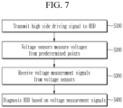
- FIG. 7 illustrates a flowchart of an HSD diagnosis method using a battery system according to one or more embodiments of the present disclosure.
- the MCU 401 may transmit the high-side driving signals HSD1_EN, HSD2_EN, HSD3_EN, and HSD4_EN to the HSD 310 (S100).
- the blocking elements 510_1, 520_1, 530_1, and 540_1 illustrated in FIG. 3 or the blocking elements 510_2, 520_2, 530_2, and 540_2 illustrated in FIG. 4 may be connected between the relays 210, 220, 230, and 240 and the node N_LS.
- the HSD 310 may include a plurality of ideal elements 3111, 3121, 3131, and 3141.
- the battery system 11 including blocking elements 510_1, 520_1, 530_1, 540_1, 510_2, 520_2, 530_2, and 540_2 or the ideal elements 3111, 3121, 3131, and 3141 may block voltage supplied to relays other than the target relay among the relays 210, 220, 230, and 240 through the node N_LS to which low-sides of the relays 210, 220, 230, and 240 are connected.
- the voltage sensors 410, 420, 430, and 440 may measure voltages from points (e.g., predetermined points) (S200).
- the points e.g., predetermined points
- the points may be a first end of each of the relays 210, 220, 230, and 240, or may be the nodes N_1, N_2, N_3, and N_4 on the ideal elements 3111, 3121, 3131, and 3141 included in the HSD 310_3.
- the diagnostic device 402 may receive the voltage measurement signals VS11, VS12, VS13, and VS14 indicating voltages measured by the voltage sensors 410, 420, 430, and 440 (S300). Each of the voltage measurement signals VS11, VS12, VS13, and VS14 may indicate a voltage measured at a point (e.g., a predetermined point) in operation S200.
- a point e.g., a predetermined point
- the diagnostic device 402 may diagnose the HSD 310 based on the received voltage measurement signals VS11, VS12, VS13, and VS14 (S400). For example, in FIG. 3 , FIG. 4 , or FIG. 6 , based on the plurality of voltage measurement signals VS11, VS12, VS13, and VS14 received in a state in which a voltage supplied to relays other than the target relay 210 among the relays 210, 220, 230, and 240 is blocked, the diagnostic device 402 may diagnose a pin-to-pin short-circuit due to a short circuit between a first pin of the HSD 310, which is connected to a wire that transmits the high-side driving signal HSD1_EN to the relay 210, and a second pin of the HSD 310, which is adjacent to the first pin and is connected to a wiring that transmits the high-side driving signal HSD2_EN to the relay 220.
- accuracy of diagnosis for the HSD 310 may be improved by allowing the blocking element 510_1, 520_1, 530_1, 540_1, 510_2, 520_2, 530_2, 540_2, or ideal element 3111, 3121, 3131, 3141 to block the voltage supplied to the relays other than the target relay.
- the BMS 400 may repeatedly perform the above-described diagnosis process while changing the target relay to diagnosis a pin-to-pin short-circuit for all pins of the HSD 310 that output high-side driving signals to the relays 210, 220, 230, and 240.
Landscapes
- Physics & Mathematics (AREA)
- General Physics & Mathematics (AREA)
- Engineering & Computer Science (AREA)
- Theoretical Computer Science (AREA)
- Power Engineering (AREA)
- Microelectronics & Electronic Packaging (AREA)
- Manufacturing & Machinery (AREA)
- Chemical & Material Sciences (AREA)
- Chemical Kinetics & Catalysis (AREA)
- Electrochemistry (AREA)
- General Chemical & Material Sciences (AREA)
- Charge And Discharge Circuits For Batteries Or The Like (AREA)
Abstract
A battery system (1, 11, 12) includes a battery pack (100), relays (210, 220, 230, 240) connected to the battery pack (100), a high-side driver, HSD, (310, 310_1, 310_2, 310_3) configured to apply a relay driving voltage (Vrly) to high-sides of the relays (210, 220, 230, 240), and a battery management system, BMS, (400) configured to diagnose the HSD (310, 310_1, 310_2, 310_3) based on a voltage measured from first ends of the relays (210, 220, 230, 240) or the HSD (310, 310_1, 310_2, 310_3).
Description
- The present disclosure relates to a diagnosis method and a battery system.
- In general, a mechanical relay may be used for opening and closing a high voltage battery output in a battery pack. The mechanical relay may be formed to include a coil stage and a high current stage, and if a current that is greater than a trip current flows through the coil, a magnetic force is generated to connect opposite terminals of the high current stage to allow a current to flow therethrough.
- The coil stage may include a large inductive reactance and a low resistance to allow a sufficient excitation current to flow to the coil, and the high-current stage may include a very small resistance to reduce power consumption and heat generation.
- A driver that drives such a relay may include a plurality of high-side drivers (HSDs) for driving a plurality of high-side switches between a plurality of relays and a relay driving power supply, and may include a low-side driver (LSD) for driving the low-side switches between the relays and a ground. Various failures may occur in an HSD, a LSD, a relay, a battery, etc. A technique for detecting these failures may be desirable.
- The present disclosure provides a diagnosis method for a high-side driver and a battery system that are capable of detecting a short circuit between a plurality of pins (hereinafter referred to as a pin-to-pin short circuit) that are for applying signals to drive a plurality of high-side switches.
- One or more embodiments of the present disclosure provide a battery system including a battery pack, relays connected to the battery pack, a high-side driver (HSD) configured to apply a relay driving voltage to high-sides of the relays, and a battery management system (BMS) configured to diagnose the HSD based on a voltage measured from first ends of the relays or the HSD.
- The battery system may further include a low-side driver (LSD) configured to connect a first node, which is connected to low-sides of the relays, and a ground (e.g., the LSD may be connected between low-sides of the relays and a ground).
- The battery system may further include voltage sensors configured to generate voltage measurement signals, wherein the BMS may include a main control unit (MCU) configured to drive the HSD to supply a voltage (e.g., the relay driving voltage) to relay coils corresponding to the relays, and a diagnostic device configured to diagnose the HSD based on the voltage measurement signals.
- The voltage sensors may be configured to measure high-side voltages of the relays (e.g., voltages from first ends of the relays), wherein the HSD may include first switching elements configured to apply the relay driving voltage to the relays.
- The battery system may further include blocking elements including a diode having an anode connected to a low-side of a corresponding one of the relays, and having a cathode connected to the first node.
- The MCU may be further configured to output driving signals (e.g., high-side driving signals) for the first switching elements to the HSD, wherein the HSD may further include drivers for outputting inverted driving signals obtained by inverting the driving signals (e.g., high-side driving signals) for the first switching elements.
- The battery system may further include blocking elements including a second switching element including a drain connected to a low-side of a corresponding one of the relays, a source connected to the first node, and a gate for receiving a corresponding one of the inverted driving signals from a corresponding one of the drivers, and a diode having an anode connected to the drain, and a cathode connected to the source.
- The voltage sensors may be configured to respectively measure voltages of the relays (e.g., corresponding voltages of the HSD), wherein the MCU may be further configured to generate high-side driving signals corresponding to the relays to transmit them to the HSD, and wherein the HSD may include elements (e.g., "ideal elements") configured to apply the relay driving voltage to the relays, and drivers configured to receive the high-side driving signals from pins to drive the elements.
- The elements (e.g., "ideal" elements") may include a first switching element configured to have a drain to which the relay driving voltage is applied, a second switching element configured to have a source connected to a source of the first switching element, and a drain connected to a high-side of one of the relays, a first diode configured to have an anode connected to the source of the first switching element, and a cathode connected to the drain of the first switching element, and a second diode configured to have an anode connected to the source of the second switching element, and a cathode connected to the drain of the second switching element, and wherein the drivers may be further configured to respectively supply voltages (e.g., gate signals) to gates of the first switching elements and to gates of the second switching elements.
- One of the voltage sensors may be further configured to generate one of the voltage measurement signals by measuring a voltage from a node to which the source of the first switching element and the source of the second switching element is connected, and to transmit the one of the voltage measurement signals to the diagnostic device.
- One or more embodiments of the present disclosure provide a diagnosis method including applying a relay driving voltage to high-sides of relays connected to a battery pack, obtaining voltage signals (e.g., voltage measurement signals) by measuring a voltage from first ends of the relays (e.g., high-side voltages of the relays) or a high-side driver (HSD), and diagnosing the HSD based on the voltage signals.
- The diagnosis method may further include connecting a first node, which is connected to low-sides of the relays, and a ground.
- The diagnosis method may further include driving the HSD to supply a voltage (e.g., the relay driving voltage) to relay coils corresponding to the relays.
- The applying of the relay driving voltage may include applying a driving signal (e.g., a high-side driving signal) to a first switching element connected to a high-side of one of the relays, wherein the first switching element may include a gate to which the driving signal (e.g., the high-side driving signal) is applied, a drain to which the relay driving voltage is applied, and a source connected to a high-side of a corresponding relay of the relays, and wherein the first switching element may be configured to transmit the relay driving voltage to the high-side of the corresponding relay based on the driving signal (e.g., the high-side driving signal).
- The applying of the relay driving voltage may further include applying an inverted driving signal, in which the driving signal (e.g., the high-side driving signal) applied to the first switching element connected to the corresponding relay is inverted, to a blocking element connected to a corresponding low-side of the low-sides of the corresponding relay, wherein the blocking element may be connected between the corresponding relay and the first node, respectively, and may include a second switching element, wherein the second switching element may include a gate for receiving the inverted driving signal, a drain connected to the corresponding low-side, and a source connected to the first node, and wherein the second switching element connects the corresponding low-side to the first node based on the inverted driving signal.
- The applying of the relay driving voltage may include receiving a high-side driving signal corresponding to a corresponding relay of the relays from a battery management system (BMS), and driving an element (e.g., an "ideal element") to apply the relay driving voltage to the corresponding relay.
- The element may include a first switching element including a drain for receiving the relay driving voltage, and a second switching element including a source connected to a source of the first switching element, and a drain connected to a high-side of the corresponding relay, and wherein the driving of the element (e.g., the "ideal element") may include supplying a voltage (e.g., a gate signal) to a gate of the first switching element and to a gate of the second switching element.
- The measuring of the voltage may include generating a voltage measurement signal by measuring a voltage from a node to which the source of the first switching element and the source of the second switching element of the element are connected, and transmitting the voltage measurement signal to the BMS.
- According to the present disclosure, it is possible to detect occurrence of a short circuit between pins while low-sides of relays are commonly operated and high-sides are independently operated.
- According to the present disclosure, reliability of diagnosis may be secured through low-side common operation of the plurality of relays, and not only may complex interfaces be simplified, and high costs may be reduced, but also fault diagnosis of HSD is possible.
- According to the present disclosure, an automotive safety integrity level (ASIL) may be improved according to reduction of failures in time (FIT) by broadening a diagnostic area of the battery system.
- All embodiments described in this specification may be advantageously combined with one another to the extent that their respective features are compatible. In particular, the expressions "according to an embodiment," "in an embodiment," "an embodiment of the invention provides" etc. mean that the respective features may or may not be part of specific embodiments of the present invention.
-
-
FIG. 1 illustrates a block diagram schematically showing a battery system according to one or more embodiments of the present disclosure. -
FIG. 2 illustrates a block diagram schematically showing a detailed configuration of the battery system ofFIG. 1 . -
FIG. 3 illustrates a circuit diagram if a blocking element included in the battery system ofFIG. 2 includes a diode. -
FIG. 4 illustrates an example circuit diagram if a blocking element included in the battery system ofFIG. 2 includes a P-channel switch. -
FIG. 5 illustrates a block diagram schematically showing an example detailed configuration of the battery system ofFIG. 1 . -
FIG. 6 illustrates an example circuit diagram if an HSD included in the battery system ofFIG. 5 includes a blocking element. -
FIG. 7 illustrates a flowchart of an HSD diagnosis method using a battery system according to one or more embodiments of the present disclosure. - Aspects of some embodiments of the present disclosure and methods of accomplishing the same may be understood more readily by reference to the detailed description of embodiments and the accompanying drawings. The described embodiments are provided as examples so that this disclosure will be thorough and complete, and will fully convey the aspects of the present disclosure to those skilled in the art. Accordingly, processes, elements, and techniques that are redundant, that are unrelated or irrelevant to the description of the embodiments, or that are not necessary to those having ordinary skill in the art for a complete understanding of the aspects of the present disclosure may be omitted. Unless otherwise noted, like reference numerals, characters, or combinations thereof denote like elements throughout the attached drawings and the written description, and thus, repeated descriptions thereof may be omitted.
- The described embodiments may have various modifications and may be embodied in different forms, and should not be construed as being limited to only the illustrated embodiments herein. The present disclosure covers all modifications, equivalents, and replacements within the idea and technical scope of the present disclosure. Further, each of the features of the various embodiments of the present disclosure may be combined with each other, in part or in whole, and technically various interlocking and driving are possible. Each embodiment may be implemented independently of each other or may be implemented together in an association.
- It will be understood that when an element, layer, region, or component is referred to as being "connected to" or "(operatively or communicatively) coupled to" another element, layer, region, or component, it can be directly connected to or coupled to the other element, layer, region, or component, or indirectly connected to or coupled to the other element, layer, region, or component such that one or more intervening elements, layers, regions, or components may be present. In addition, this may collectively mean a direct or indirect coupling or connection and an integral or non-integral coupling or connection. For example, when a layer, region, or component is referred to as being "electrically connected" or "electrically coupled" to another layer, region, or component, it can be directly electrically connected or coupled to the other layer, region, and/or component or intervening layers, regions, or components may be present. However, "directly connected/directly coupled" refers to one component directly connecting or coupling another component without an intermediate component.
- It will be understood that when an element or layer is referred to as being "between" two elements or layers, it can be the only element or layer between the two elements or layers, or one or more intervening elements or layers may also be present.
- For the purposes of this disclosure, expressions, such as "at least one of," or "any one of," or "one or more of" when preceding a list of elements, modify the entire list of elements and do not modify the individual elements of the list. For example, "at least one of X, Y, and Z," "at least one of X, Y, or Z," "at least one selected from the group consisting of X, Y, and Z," and "at least one selected from the group consisting of X, Y, or Z" may be construed as X only, Y only, Z only, any combination of two or more of X, Y, and Z, such as, for instance, XYZ, XYY, YZ, and ZZ, or any variation thereof. Similarly, the expression, such as "at least one of A and B" and "at least one of A or B" may include A, B, or A and B. As used herein, "or" generally means "and/or," and the term "and/or" includes any and all combinations of one or more of the associated listed items. For example, the expression, such as "A and/or B" may include A, B, or A and B. Similarly, expressions, such as "at least one of," "a plurality of," "one of," and other prepositional phrases, when preceding a list of elements, modify the entire list of elements and do not modify the individual elements of the list.
- It will be understood that, although the terms "first," "second," "third," etc., may be used herein to describe various elements, components, regions, layers and/or sections, these elements, components, regions, layers and/or sections should not be limited by these terms. These terms do not correspond to a particular order, position, or superiority, and are used only used to distinguish one element, member, component, region, area, layer, section, or portion from another element, member, component, region, area, layer, section, or portion. Thus, a first element, component, region, layer or section described below could be termed a second element, component, region, layer or section, without departing from the scope of the present disclosure. The description of an element as a "first" element may not require or imply the presence of a second element or other elements. The terms "first," "second," etc. may also be used herein to differentiate different categories or sets of elements. For conciseness, the terms "first," "second," etc. may represent "first-category (or first-set)," "second-category (or secondset)," etc., respectively.
- The terminology used herein is for the purpose of describing embodiments only and is not intended to be limiting of the present disclosure. As used herein, the singular forms "a" and "an" are intended to include the plural forms as well, while the plural forms are also intended to include the singular forms, unless the context clearly indicates otherwise. It will be further understood that the terms "comprises," "comprising," "have," "having," "includes," and "including," when used in this specification, specify the presence of the stated features, integers, steps, operations, elements, and/or components, but do not preclude the presence or addition of one or more other features, integers, steps, operations, elements, components, and/or groups thereof.
- When one or more embodiments may be implemented differently, a specific process order may be performed differently from the described order. For example, two consecutively described processes may be performed substantially at the same time or performed in an order opposite to the described order.
- As used herein, the term "substantially," "about," "approximately," and similar terms are used as terms of approximation and not as terms of degree, and are intended to account for the inherent deviations in measured or calculated values that would be recognized by those of ordinary skill in the art. "About" or "approximately," as used herein, is inclusive of the stated value and means within an acceptable range of deviation for the particular value as determined by one of ordinary skill in the art, considering the measurement in question and the error associated with measurement of the particular quantity (i.e., the limitations of the measurement system). For example, "about" may mean within one or more standard deviations, or within ± 30%, 20%, 10%, 5% of the stated value. Further, the use of "may" when describing embodiments of the present disclosure refers to "one or more embodiments of the present disclosure."
- In some embodiments well-known structures and devices may be described in the accompanying drawings in relation to one or more functional blocks (e.g., block diagrams), units, and/or modules to avoid unnecessarily obscuring various embodiments. Those skilled in the art will understand that such block, unit, and/or module are/is physically implemented by a logic circuit, an individual component, a microprocessor, a hard wire circuit, a memory element, a line connection, and other electronic circuits. This may be formed using a semiconductor-based manufacturing technique or other manufacturing techniques. The block, unit, and/or module implemented by a microprocessor or other similar hardware may be programmed and controlled using software to perform various functions discussed herein, optionally may be driven by firmware and/or software. In addition, each block, unit, and/or module may be implemented by dedicated hardware, or a combination of dedicated hardware that performs some functions and a processor (for example, one or more programmed microprocessors and related circuits) that performs a function different from those of the dedicated hardware. In addition, in some embodiments, the block, unit, and/or module may be physically separated into two or more interact individual blocks, units, and/or modules without departing from the scope of the present disclosure. In addition, in some embodiments, the block, unit and/or module may be physically combined into more complex blocks, units, and/or modules without departing from the scope of the present disclosure.
- A program implemented as a set of commands embodying a control algorithm suitable for controlling a second element may be installed in a first element for controlling the second element under a specific control condition among elements according to one or more embodiments. A control element may process input data and stored data depending on an installed program to generate output data. The control element may include a non-volatile memory to store a program and a memory to store data.
- Unless otherwise defined, all terms (including technical and scientific terms) used herein have the same meaning as commonly understood by one of ordinary skill in the art to which the present disclosure belongs. It will be further understood that terms, such as those defined in commonly used dictionaries, should be interpreted as having a meaning that is consistent with their meaning in the context of the relevant art and/or the present specification, and should not be interpreted in an idealized or overly formal sense, unless expressly so defined herein.
-
FIG. 1 illustrates a block diagram schematically showing a battery system according to one or more embodiments of the present disclosure. - The
battery system 1 may include abattery pack 100, a relay bank (e.g., relay unit) 200, arelay driver 300, and a battery management system (BMS) 400. - An
external device 2 may include a load, such as an inverter or a converter and/or a charging device. For example, opposite ends P+ and P- of thebattery system 1 may be connected to a charger to receive power from the charger and may be charged. In one or more embodiments, both ends P+ and P- of thebattery system 1 may be connected to a load to allow a power supplied by thebattery pack 100 to be discharged through the load. - The
battery pack 100 may include a plurality of battery cells connected in series and/or in parallel. - The
relay bank 200 may include a plurality of relays connected to thebattery pack 100. A first end of therelay bank 200 may be connected to thebattery pack 100, and a second end of therelay bank 200 may be connected to one of opposite ends of thebattery system 1. Therelay bank 200 may include a plurality of relays among at least one first relay connected between a first end (+ terminal) of thebattery pack 100 and a first end (P+) of thebattery system 1, and may include at least one second relay connected between the other end (- terminal) of thebattery pack 100 and a second end (P-) of thebattery system 1. Hereinafter, a number of relays included in therelay bank 200 will be described as plural. - The
relay driver 300 may drive therelay bank 200 under control of theBMS 400. Therelay driver 300 may include a plurality of high-side drivers (HSDs) and low-side drivers (LSDs). The HSDs may drive a high-side switch between a plurality of relays included in therelay driver 300 and a relay driving voltage for driving the relays. The LSDs may drive a low-side switch between the multiple relays and a ground. - The
relay driver 300 may drive each of the relays included in therelay bank 200 at a high-side of each of the relays while commonly operating a low-side of therelay bank 200. Therelay driver 300 may include a blocking element in a high-side channel corresponding to each of the relays. Therelay driver 300 enables independent diagnosis of the HSDs corresponding to the relays by blocking a voltage and/or a current through a blocking element corresponding to the remaining relays with the exception of one relay to be monitored among the relays. - The
BMS 400 may control an operation of therelay driver 300, and may diagnose a plurality of HSDs. TheBMS 400 may control an operation of therelay driver 300, including, for example, a plurality of HSDs, LSDs, and blocking elements. TheBMS 400 also may monitor a voltage and/or a current in therelay bank 200 and/or therelay driver 300. TheBMS 400 also may diagnose therelay driver 300 based on a measured voltage. TheBMS 400 may measure voltages from first ends of the relays included in therelay bank 200, and may measure currents from wires included in therelay driver 300. TheBMS 400 may diagnose a state of the HSDs included in therelay driver 300 by diagnosing therelay driver 300. -
FIG. 2 illustrates a block diagram schematically showing a detailed configuration of the battery system ofFIG. 1 . - Hereinafter, a detailed configuration of a
battery system 11, which shows an example in which the blocking element is connected to a first end of therelay driver 300 in thebattery system 1 ofFIG. 1 , will be described with reference toFIG. 2 . - The
battery system 11 illustrated inFIG. 2 is an example of thebattery system 1 ofFIG. 1 . Hereinafter, among descriptions of thebattery system 11, descriptions of overlapping portions with those of thebattery system 1 may be omitted. - The
battery system 11 may include abattery pack 100, arelay bank 200, arelay driver 300, and aBMS 400. - The
relay bank 200 may include a plurality ofrelays voltage sensors elements voltage sensors HSD 310, or may be distinguished from theHSD 310 and therelay 220. - In
FIG. 2 , thevoltage sensors relays - The
relay driver 300 may include anHSD 310 and anLSD 320. TheBMS 400 may include a main control unit (MCU) 401 and a diagnostic device (e.g., a diagnosis unit) 402. Theexternal device 2 may include a capacitor C1 and a capacitor C2. - The
relay 210 may be a positive pre-charge relay. A first end of therelay 210 may be connected to a positive terminal (+) of thebattery pack 100, and a second end of therelay 210 may be connected to a first end of the capacitor C2. Therelay 210 may include arelay coil 211. - The
relay 220 may be a positive main relay. A first end of therelay 220 may be connected to a positive terminal (+) of thebattery pack 100, and a second end of therelay 220 may be connected to a first end of the capacitor C1. Therelay 220 may include arelay coil 221. - The
relay 230 may be a negative main relay. A first end of therelay 230 may be connected to a negative terminal (-) of thebattery pack 100, and a second end of therelay 230 may be connected to a second end of the capacitor C1. Therelay 230 may include arelay coil 231. - The
relay 240 may be a negative pre-charge relay. A first end of therelay 240 may be connected to a negative terminal (-) of thebattery pack 100, and a second end of therelay 240 may be connected to a second end of the capacitor C2. Therelay 240 may include arelay coil 241. - The
HSD 310 may supply relay coil voltages to the relay coils 211, 221, 231, and 241. - The
HSD 310 may include a plurality of terminals P11, P12, P13, and P14. Each of the terminals P11, P12, P13, and P14 may correspond to a pin of theHSD 310. - A low voltage power source LV may be supplied to the
HSD 310. For example, the low voltage power source LV may be an auxiliary voltage of a vehicle. - The
MCU 401 may generate and transmit a plurality of high-side driving signals HSD1_EN, HSD2_EN, HSD3_EN, and HSD4_EN to theHSD 310. TheMCU 401 may drive theHSD 310 to supply a voltage to each of the relay coils 211, 221, 231, and 241. - The
HSD 310 may supply a relay coil voltage to a high-side (first end) of each of the relay coils 211, 221, 231, and 241 through the terminals P11, P12, P13, and P14 according to multiple high-side driving signals HSD1_EN, HSD2_EN, HSD3_EN, and HSD4_EN. For example, upon receiving an on-level high-side driving signal HSD1_EN from theMCU 401, theHSD 310 may apply an on-level relay coil voltage to a high-side of therelay coil 211 through the terminal P11. - A corresponding relay among the
relays relays MCU 401 through the high-side driving signals HSD1_EN, HSD2_EN, HSD3_EN, and HSD4_EN is referred to as a target relay. - Each of a plurality of blocking
elements elements relays - In
FIG. 2 , each of the blockingelements elements HSD 310 to block a voltage supplied to the remaining relays excluding the target relay among therelays - In one or more embodiments, in
FIG. 2 , numbers of therelays elements relays voltage sensors battery system 11 may include a plurality of relays, a plurality of blocking elements, and a plurality of voltage sensors. In some embodiments, a number of the blocking elements may correspond to the number of the relays, and a number of the voltage sensors may also correspond to the number of relays. For example, if there are 4 relays, thebattery system 11 may also include 4 blocking elements and 4 voltage sensors. - The
MCU 401 may generate and transmit a low-side driving signal LSD_EN to anLSD 320. TheLSD 320 may connect low-sides of the relay coils 211, 221, 231, and 241 to the ground according to the low-side driving signal LSD_EN. - A first end (high-side) of each of the relay coils 211, 221, 231, and 241 is connected to the
HSD 310, and a second end (low-side) of each of the relay coils 211, 221, 231, and 241 may be connected to theLSD 320. - Among the
voltage sensors voltage sensor 410 may generate a voltage measurement signal VS1 by measuring a voltage of therelay coil 211 at a first end. Thevoltage sensor 420 may generate a voltage measurement signal VS2 by measuring a voltage of therelay coil 221 at a first end. Thevoltage sensor 430 may generate a voltage measurement signal VS3 by measuring a voltage of therelay coil 231 at a first end. Thevoltage sensor 440 may generate a voltage measurement signal VS4 by measuring a voltage of therelay coil 241 at a first end. - The
voltage sensors diagnostic device 402. Thediagnostic device 402 may diagnose theHSD 310 and/or therelays - In
FIG. 2 , each of thevoltage sensors relays relays - Hereinafter, a circuit diagram of a relay and a relay driver included in the
battery system 11 ofFIG. 2 will be described with reference toFIG. 3 andFIG. 4 . -
FIG. 3 illustrates an example circuit diagram if a blocking element included in the battery system ofFIG. 2 includes a diode. - Referring to
FIG. 3 , therelay bank 200 and therelay driver 300 ofFIG. 2 may include a plurality ofrelays LSD 320, and a plurality ofvoltage sensors - The HSD 310_1 of
FIG. 3 may be an example of theHSD 310 ofFIG. 2 , and the blocking elements 510_1, 520_1, 530_1, and 540_1 ofFIG. 3 may be an example of the blockingelements FIG. 2 . - Hereinafter, for better understanding and ease of description, a high-side (first end) of the
relay 210 is called a node N_HS1, a high-side (first end) of therelay 220 is called a node N_HS2, a high-side (first end) of therelay 230 is called a node N_HS3, and a high-side (first end) of therelay 240 is referred to as a node N_HS4. In one or more embodiments, a low-side (second end) of each of therelays - The
relay 210 may include arelay coil 211 and a resistor R1. Therelay 220 may include arelay coil 221 and a resistor R2. Therelay 230 may include arelay coil 231 and a resistor R3. Therelay 240 may include arelay coil 241 and a resistor R4. - The HSD 310_1 may include a plurality of switching elements M1, M2, M3, and M4. The switching elements M1, M2, M3, and M4 may be N-channel metal-oxide-semiconductor field effect transistors (MOSFETs). The switching elements M1, M2, M3, and M4 may correspond to the
relays - The switching elements M1, M2, M3, and M4 may respectively receive the high-side driving signals HSD1_EN, HSD2_EN, HSD3_EN, and HSD4_EN from the
MCU 401 ofFIG. 2 through pins of the HSD 310_1. - The high-side driving signal HSD1_EN may be applied to a gate of the switching element M1. A relay driving voltage Vrly may be applied to the drain of the switching element M1, and the first end of the
relay 210 may be connected to a source of the switching element M1. If the on-level high-side driving signal HSD1_EN is applied, a potential difference between a gate and a source becomes more than a threshold voltage (e.g., a predetermined threshold voltage), and thus the switching element M1 is turned on, and the relay driving voltage Vrly may be applied to therelay 210 through the turned-on switching element M1. Hereinafter, the relay driving voltage Vrly ofFIG. 3 may be a voltage according to a low voltage power source LV ofFIG. 2 . - A high-side driving signal HSD2_EN may be applied to a gate of the switching element M2. The relay driving voltage Vrly may be applied to a drain of the switching element M2, and a first end of the
relay 220 may be connected to a source of the switching element M2. If the on-level high-side driving signal HSD2_EN is applied, a potential difference between a gate and a source becomes more than a threshold voltage (e.g., a predetermined threshold voltage), and thus the switching element M2 is turned on, and the relay driving voltage Vrly may be applied to therelay 220 through the turned-on switching element M2. - A high-side driving signal HSD3_EN may be applied to a gate of the switching element M3. The relay driving voltage Vrly may be applied to a drain of the switching element M3, and a first end of the
relay 230 may be connected to a source of the switching element M3. If the on-level high-side driving signal HSD3_EN is applied, a potential difference between a gate and a source becomes more than a threshold voltage (e.g., a predetermined threshold voltage), and thus the switching element M3 is turned on, and the relay driving voltage Vrly may be applied to therelay 230 through the turned-on switching element M3. - A high-side driving signal HSD4_EN may be applied to a gate of the switching element M4. The relay driving voltage Vrly may be applied to a drain of the switching element M4, and a first end of the
relay 240 may be connected to a source of the switching element M4. If the on-level high-side driving signal HSD4_EN is applied, a potential difference between a gate and a source becomes more than a threshold voltage (e.g., a predetermined threshold voltage), and thus the switching element M4 is turned on, and the relay driving voltage Vrly may be applied to therelay 240 through the turned-on switching element M4. - The
LSD 320 may include a switching element M5. The switching element M5 may be an N-channel MOSFET. A plurality of switching elements M5 may receive the low-side driving signal LSD_EN from theMCU 401 ofFIG. 2 . - A low-side driving signal LSD_EN may be applied to a gate of the switching element M5. Second ends of the
relays relays - The
voltage sensors voltage sensor 410 may include a buffer and anADC 411. - Each of the
ADCs ADC 451 may measure the voltage of the node N_LS and may generate a voltage measurement signal VS21 representing the measured voltage. - The
ADCs diagnostic device 402 ofFIG. 2 . Thediagnostic device 402 may receive the voltage measurement signals VS11, VS12, VS13, VS14 and VS21, and may diagnose the HSD 310_1 based on them. - The blocking element 510_1 may include a diode D1. An anode of the diode D1 may be connected to the low-side of the
relay 210, and a cathode of the diode D1 may be connected to the node N_LS. - The blocking element 520_1 may include a diode D2. An anode of the diode D2 may be connected to the low-side of the
relay 220, and a cathode of the diode D2 may be connected to the node N_LS. - The blocking element 530_1 may include a diode D3. An anode of the diode D3 may be connected to the low-side of the
relay 230, and a cathode of the diode D3 may be connected to the node N_LS. - The blocking element 540_1 may include a diode D4. An anode of the diode D4 may be connected to the low-side of the
relay 240, and a cathode of the diode D4 may be connected to the node N_LS. - The
MCU 401 may operate the switching elements M1 to M5 through the high-side driving signals HSD1_EN, HSD2_EN, HSD3_EN, and HSD4_EN and the low-side driving signal LSD_EN, and may supply the relay driving voltage Vrly to a target relay (e.g., relay 210) among therelays diagnostic device 402 may derive a high-side voltage of each of the plurality ofrelays - Hereinafter, a case in which the relay driving voltage Vrly is supplied to the
target relay 210 will be described as an example. - Assuming a comparative example in which the
relay bank 200 and therelay driver 300 ofFIG. 3 do not include the blocking elements 510_1, 520_1, 530_1, and 540_1, a current flowing in thetarget relay 210 according to the relay driving voltage Vrly may flow to the remainingrelays relays diagnostic device 402 has difficulty determining whether a short circuit between pins of the HSD 310_1 has occurred based on the voltage measurement signals VS12, VS13, and VS14. - In one or more embodiments, referring to
FIG. 3 , in one or more embodiments, the blocking elements 510_1, 520_1, 530_1, and 540_1 may be included to block a current flowing in the direction of the diodes D1, D2, D3, and D4 from the node N_LS toward therelays relays target relay 210 and the nodes N_HS2, N_HS3, and N_HS4 corresponding to the remainingrelays diagnostic device 402 may determine whether a short circuit between the pins of the HSD 310_1 has occurred based on the voltage measurement signals VS12, VS13, and VS14. - For example, if there is a relay (e.g., relay 220) exhibiting a same voltage as the high-side voltage of the target relay (e.g., relay 210) among the high-side voltages of the remaining relays (e.g., relays 220, 230, and 240), the
diagnostic device 402 may diagnose that a short circuit between pins corresponding to a corresponding relay (e.g., relay 220) among the pins of the HSD 310_1 has occurred. - In
FIG. 3 , therelay driver 300 includes an HSD 310_1, the HSD 310_1 includes a plurality of switching elements M1, M2, M3, and M4, and the switching elements M1, M2, M3, and M4 are illustrated as being controlled by the high-side driving signals HSD1_EN, HSD2_EN, HSD3_EN, and HSD4_EN, but the present disclosure is not limited thereto. In some embodiments, therelay driver 300 may include a plurality of HSDs, each of the HSDs may include a switching element, and the switching element included in each of the HSDs may be controlled by the high-side driving signals HSD1_EN, HSD2_EN, HSD3_EN, and HSD4_EN. -
FIG. 4 illustrates an example circuit diagram if a blocking element included in the battery system ofFIG. 2 includes a P-channel switch. - Among the descriptions of
FIG. 4 , descriptions of portions overlapping the previous description ofFIG. 3 may be omitted. - Referring to
FIG. 4 , therelay bank 200 and therelay driver 300 ofFIG. 2 may include a plurality ofrelays LSD 320, a plurality ofvoltage sensors FIG. 4 may be an example of theHSD 310 ofFIG. 2 , and the blocking elements 510_2, 520_2, 530_2, and 540_2 ofFIG. 4 may be an example of the blockingelements FIG. 2 . - The HSD 310_2 may include a plurality of switching elements M1, M2, M3, and M4 and a plurality of
drivers relays - The switching elements M1, M2, M3, and M4 and the
drivers MCU 401 ofFIG. 2 through pins of the HSD 310_2. - The
drivers - The blocking element 510_2 may include the switching element M11 and the diode D5. A first end of the
driver 3110 may be connected to a gate of the switching element M1, and a second end of thedriver 3110 may be connected to a gate of the switching element M11. An anode of the diode D5 may be connected to the drain of the switching element M11, and a cathode of the diode D5 may be connected to a source of the switching element M11. - The blocking element 520_2 may include the switching element M12 and the diode D6. A first end of the
driver 3120 may be connected to a gate of the switching element M2, and a second end of thedriver 3120 may be connected to a gate of the switching element M12. An anode of the diode D6 may be connected to the drain of the switching element M12, and a cathode of the diode D6 may be connected to a source of the switching element M12. - The blocking element 530_2 may include a switching element M13 and a diode D7. A first end of the
driver 3130 may be connected to a gate of the switching element M3, and a second end of thedriver 3130 may be connected to a gate of the switching element M13. An anode of the diode D7 may be connected to the drain of the switching element M13, and a cathode of the diode D7 may be connected to a source of the switching element M13. - The blocking element 540_2 may include the switching element M14 and the diode D8. A first end of the
driver 3140 may be connected to a gate of the switching element M4, and a second end of thedriver 3140 may be connected to a gate of the switching element M14. An anode of the diode D8 may be connected to the drain of the switching element M14, and a cathode of the diode D8 may be connected to a source of the switching element M14. - The switching elements M11, M12, M13, and M14 may be P-channel MOSFETs.
- If the corresponding high-side driving signal (e.g., HSD1_EN) among the high-side driving signals HSD1_EN, HSD2_EN, HSD3_EN, and HSD4_EN is at an on level, each of the
drivers - For example, the
drivers drivers - If the on-level high-side driving signal HSD1_EN is applied, the switching element M1 is turned on, the switching element M11 is turned off, and the diode D5 is conducted, and thus the relay driving voltage Vrly may be applied to the
relay 210. - If the on-level high-side driving signal HSD2_EN is applied, the switching element M2 is turned on, the switching element M12 is turned off, and the diode D6 is conducted, and thus the relay driving voltage Vrly may be applied to the
relay 220. - If the on-level high-side driving signal HSD3_EN is applied, the switching element M3 is turned on, the switching element M13 is turned off, and the diode D7 is conducted, and thus the relay driving voltage Vrly may be applied to the
relay 230. - If the on-level high-side driving signal HSD4_EN is applied, the switching element M4 is turned on, the switching element M14 is turned off, and the diode D8 is conducted, and thus the relay driving voltage Vrly may be applied to the
relay 240. - Referring to
FIG. 4 , the blocking elements 510_2, 520_2, 530_2, and 540_2 may generate less heat by using the switching elements M11, M12, M13, and M14 that are P-channel MOSFET compared to the blocking elements 510_1, 520_1, 530_1, and 540_1 illustrated inFIG. 3 . For example, inFIG. 3 , heat generated from the blocking element 510_1 is obtained by an equation Ploss_3 = Vf*IL. Herein, IL indicates a current flowing in therelay coil 211 of thetarget relay 210, and Vf indicates a diode voltage due to characteristics of diode D1. In one or more embodiments, inFIG. 4 , heat generated from the blocking element 510_2 may be obtained by an equation Ploss_4 =IL2*Rds_on. Herein, IL indicates a current flowing through therelay coil 211 of thetarget relay 210, and Rds_on indicates a drain-source resistance if the switching element M11 is turned on. - Referring to
FIG. 4 , in one or more embodiments, the blocking elements 510_2, 520_2, 530_2, 540_2 may be included to block a current flowing in a direction in which the switching elements M11, M12, M13, and M14 and the diodes D5, D6, D7, and D8 are directed from the node N_LS toward therelays relays target relay 210 and the nodes N_HS2 to N_HS4 corresponding to the remainingrelays diagnostic device 402 may determine whether a short circuit between the pins of the HSD 310_2 has occurred based on the voltage measurement signals VS12, VS13, and VS14. - In
FIG. 4 , therelay driver 300 includes an HSD 310_2, the HSD 310_2 includes the switching elements M1, M2, M3, and M4 and thedrivers drivers relay driver 300 may include a plurality of HSDs, each of the HSDs may include a switching element and a driver, and the switching element and the driver included in each of the HSDs may be controlled by the high-side driving signals HSD1_EN, HSD2_EN, HSD3_EN, and HSD4_EN. -
FIG. 5 illustrates a block diagram schematically showing a detailed configuration of the battery system ofFIG. 1 . - Hereinafter, a detailed configuration of the
battery system 12 showing an example in which a blocking element is included in therelay driver 300 in thebattery system 1 ofFIG. 1 will be described with reference toFIG. 5 . - The
battery system 12 illustrated inFIG. 5 is an example of thebattery system 1 ofFIG. 1 . Hereinafter, among descriptions of thebattery system 12, descriptions of overlapping or repeated portions with those of thebattery system - The
battery system 12 may include abattery pack 100, arelay bank 200, arelay driver 300, and aBMS 400. - The
relay bank 200 may include a plurality ofrelays voltage sensors - In
FIG. 5 , thevoltage sensors HSD 310. - The
relay driver 300 may include anHSD 310 and anLSD 320. TheBMS 400 may include anMCU 401 and adiagnostic device 402. Theexternal device 2 may include a capacitor C1 and a capacitor C2. - Hereinafter, a circuit diagram of a relay and a relay driver included in the
battery system 12 ofFIG. 5 will be described with reference toFIG. 6 . -
FIG. 6 illustrates an example circuit diagram if an HSD included in the battery system ofFIG. 5 includes a blocking element. - Referring to
FIG. 6 , therelay bank 200 and therelay driver 300 ofFIG. 5 may include a plurality ofrelays LSD 320, and a plurality ofvoltage sensors - The HSD 310_3 of
FIG. 6 may be an example of theHSD 310 ofFIG. 5 . - The HSD 310_3 may include a plurality of
drivers elements - Referring to
FIG. 6 , in thebattery system 12, theideal elements relays - The
ideal element 3111 includes two switching elements NM1_1 and NM1_2 and two diodes D1_1 and D1_2. Theideal element 3121 includes two switching elements NM2_1 and NM2_2 and two diodes D2_1 and D2_2. Theideal element 3131 includes two switching elements NM3_1 and NM3_2 and two diodes D3_1 and D3_2. Theideal element 3141 may include two switching elements NM4_1 and NM4_2 and two diodes D4_1 and D4_2. The switching elements NM1_1, NM1_2, NM2_1, NM2_2, NM3_1, NM3_2, NM4_1, and NM4_2 may be N-channel MOSFETs. - The
drivers MCU 401 ofFIG. 5 through pins of the HSD 310_3. - The
drivers ideal elements - The
driver 3110 may generate gate signals GS11 and GS12 based on the high-side driving signal HSD1_EN to transmit the gate signals GS11 and GS12 to theideal element 3111. Thedriver 3120 may generate gate signals GS21 and GS22 based on the high-side driving signal HSD2_EN to transmit the gate signals GS21 and GS22 to theideal element 3121. Thedriver 3130 may generate gate signals GS31 and GS32 based on the high-side driving signal HSD3_EN to transmit the gate signals GS31 and GS32 to theideal element 3131. Thedriver 3140 may generate gate signals GS41 and GS42 based on the high-side driving signal HSD4_EN to transmit the gate signals GS41 and GS42 to theideal element 3141. - Hereinafter, the relay driving voltage Vrly of
FIG. 6 may be a voltage according to a low voltage power source LV ofFIG. 5 . - The gate signal GS11 may be applied to the gate of the switching element NM1_1, and the gate signal GS12 may be applied to a gate of the switching element NM1_2. The relay driving voltage Vrly may be applied to a drain of the switching element NM1_1, and a cathode of the diode D1_1 may be connected thereto. A source of the switching element NM1_1, a source of the switching element NM1_2, an anode of the diode D1_1, and an anode of the diode D1_2 may be connected to the node N_1. A drain of the switching element NM1_2 may be connected to a cathode of the diode D1_2 and one end of the
relay 210. - The gate signal GS21 may be applied to the gate of the switching element NM2_1, and the gate signal GS22 may be applied to a gate of the switching element NM2_2. The relay driving voltage Vrly may be applied to a drain of the switching element NM2_1, and a cathode of the diode D2_1 may be connected thereto. A source of the switching element NM2_1, a source of the switching element NM2_2, an anode of the diode D2_1, and an anode of the diode D2_2 may be connected to the node N_2. A drain of the switching element NM2_2 may be connected to a cathode of the diode D2_2 and one end of the
relay 220. - The gate signal GS31 may be applied to the gate of the switching element NM3_1, and the gate signal GS32 may be applied to a gate of the switching element NM3_2. The relay driving voltage Vrly may be applied to a drain of the switching element NM3_1, and a cathode of the diode D3_1 may be connected thereto. A source of the switching element NM3_1, a source of the switching element NM3_2, an anode of the diode D3_1, and an anode of the diode D3_2 may be connected to the node N_3. A drain of the switching element NM3_2 may be connected to a cathode of the diode D3_2 and one end of the
relay 230. - The gate signal GS41 may be applied to the gate of the switching element NM4_1, and the gate signal GS42 may be applied to a gate of the switching element NM4_2. The relay driving voltage Vrly may be applied to a drain of the switching element NM4_1, and a cathode of the diode D4_1 may be connected thereto. A source of the switching element NM4_1, a source of the switching element NM4_2, an anode of the diode D4_1, and an anode of the diode D4_2 may be connected to the node N_4. A drain of the switching element NM4_2 may be connected to a cathode of the diode D4_2 and one end of the
relay 240. - The
drivers ideal elements - For example, the
driver 3110 may transmit two on-level gate signals GS11 and GS12 to theideal element 3111 based on the on-level high-side driving signal HSD1_EN. Upon receiving the on-level gate signals GS11 and GS12, theideal element 3111 may apply the relay driving voltage Vrly to therelay 210. - The
voltage sensors voltage sensor 410 may include a buffer and anADC 411. - Each of the
ADCs ADC 451 may measure the voltage of the node N_LS, and may generate a voltage measurement signal VS21 representing the measured voltage. - The
ADCs diagnostic device 402 ofFIG. 5 . Thediagnostic device 402 may receive the voltage measurement signals VS11, VS12, VS13, VS14 and VS21, and may diagnose the HSD 310_3 based thereon. - Referring to
FIG. 6 , a small amount of heat may be generated by using a plurality of switching elements NM1_1, NM1_2, NM2_1, NM2_2, NM3_1, NM3_2, NM4_1, and NM4_2, which are N-channel MOSFETs, as compared to the blocking elements 510_2, 520_2, 530_2, and 540_2 illustrated inFIG. 4 . In one or more embodiments, inFIG. 6 , heat generated from theideal element 3111 may be obtained by an equation Ploss_6 =IL2*Rds_on. Herein, IL indicates a current flowing through therelay coil 211 of thetarget relay 210, and Rds_on indicates a drain-source resistance if theideal element 3111 is turned on. In the circuit diagram ofFIG. 6 , a Rds_on value may be relatively lower than that of the P-channel MOSFET ofFIG. 4 by using an N-channel MOSFET. - As described above, referring to
FIG. 2 to FIG. 4 , thevoltage sensors relays FIG. 5 andFIG. 6 , may measure voltages from the nodes N_1, N_2, N_3, and N_4 on theHSD 310. -
FIG. 7 illustrates a flowchart of an HSD diagnosis method using a battery system according to one or more embodiments of the present disclosure. - Hereinafter, the flowchart of
FIG. 7 will be described with reference to thebattery system 11 ofFIG. 2 and/or thebattery system 12 ofFIG. 5 . Hereinafter, among descriptions of thebattery system 11 and/or thebattery system 12 ofFIG. 5 , descriptions of overlapping portions with the previous descriptions may be omitted. - The
MCU 401 may transmit the high-side driving signals HSD1_EN, HSD2_EN, HSD3_EN, and HSD4_EN to the HSD 310 (S100). - The blocking elements 510_1, 520_1, 530_1, and 540_1 illustrated in
FIG. 3 or the blocking elements 510_2, 520_2, 530_2, and 540_2 illustrated inFIG. 4 may be connected between therelays - In one or more embodiments, referring to
FIG. 6 , theHSD 310 may include a plurality ofideal elements - As such, the
battery system 11 including blocking elements 510_1, 520_1, 530_1, 540_1, 510_2, 520_2, 530_2, and 540_2 or theideal elements relays relays - The
voltage sensors relays ideal elements - The
diagnostic device 402 may receive the voltage measurement signals VS11, VS12, VS13, and VS14 indicating voltages measured by thevoltage sensors - The
diagnostic device 402 may diagnose theHSD 310 based on the received voltage measurement signals VS11, VS12, VS13, and VS14 (S400). For example, inFIG. 3 ,FIG. 4 , orFIG. 6 , based on the plurality of voltage measurement signals VS11, VS12, VS13, and VS14 received in a state in which a voltage supplied to relays other than thetarget relay 210 among therelays diagnostic device 402 may diagnose a pin-to-pin short-circuit due to a short circuit between a first pin of theHSD 310, which is connected to a wire that transmits the high-side driving signal HSD1_EN to therelay 210, and a second pin of theHSD 310, which is adjacent to the first pin and is connected to a wiring that transmits the high-side driving signal HSD2_EN to therelay 220. - As described above, accuracy of diagnosis for the
HSD 310 may be improved by allowing the blocking element 510_1, 520_1, 530_1, 540_1, 510_2, 520_2, 530_2, 540_2, orideal element - The
BMS 400 may repeatedly perform the above-described diagnosis process while changing the target relay to diagnosis a pin-to-pin short-circuit for all pins of theHSD 310 that output high-side driving signals to therelays - While according to embodiments of the present disclosure have been described in connection with what is presently considered to be practical embodiments, it is to be understood that the disclosure is not limited to the disclosed embodiments, but, on the contrary, is intended to cover various modifications and equivalent arrangements included within the scope of the appended claims, with functional equivalents thereof to be included therein.
-
- 1, 11, 12: battery system
- 100: battery pack
- 200: relay bank
- 210, 220, 230, 240: relay
- 211, 221, 231, 241: relay coil
- 300: relay driver
- 310, 310_1, 310_2, 310_3: high-side driver (HSD)
- 3110, 3120, 3130, 3140: driver
- 3111, 3121, 3131, 3141: ideal element
- 320: low-side driver (LSD)
- 400: battery management system (BMS)
- 410, 420, 430, 440, 450: voltage sensor
- 411, 421, 431, 441, 451: analog-digital converter (ADC)
- 510, 510_1, 510_2, 520, 520_1, 520_2,
- 530, 530_1, 530_2, 540, 540_1, 540_2: blocking element
- 2: external device
Claims (15)
- A battery system (1, 11, 12) comprising:a battery pack (100);relays (210, 220, 230, 240) connected to the battery pack (100);a high-side driver, HSD, (310, 310_1, 310_2, 310_3) configured to apply a relay driving voltage (Vrly) to high-sides of the relays (210, 220, 230, 240); anda battery management system, BMS, (400) configured to diagnose the HSD (310, 310_1, 310_2, 310_3) based on a voltage measured from first ends of the relays (210, 220, 230, 240) or the HSD (310, 310_1, 310_2, 310_3).
- The battery system (1, 11, 12) as claimed in claim 1, further comprising:a low-side driver, LSD, (320) configured to connect a first node (N_LS), which is connected to low-sides of the relays (210, 220, 230, 240) and a ground; andvoltage sensors (410, 420, 430, 440, 450) configured to generate voltage measurement signals (VS1, VS11, VS12, VS13, VS14, VS2, VS21, VS3, VS4),wherein the BMS (400) comprises:a main control unit, MCU, (401) configured to drive the HSD (310, 310_1, 310_2, 310_3) to supply a voltage to relay coils (211, 221, 231, 241) corresponding to the relays (210, 220, 230, 240); anda diagnostic device (402) configured to diagnose the HSD (310, 310_1, 310_2, 310_3) based on the voltage measurement signals (VS1, VS11, VS12, VS13, VS14, VS2, VS21, VS3, VS4).
- The battery system (1, 11, 12) as claimed in claim 2, wherein the voltage sensors (410, 420, 430, 440, 450) are configured to measure voltages from first ends of the relays (210, 220, 230, 240), and
wherein the HSD (310, 310_1, 310_2, 310_3) comprises first switching elements (M1, M2, M3, M4) configured to apply the relay driving voltage (Vrly) to the relays (210, 220, 230, 240). - The battery system (1, 11, 12) as claimed in claim 3, further comprising blocking elements (510, 510_1, 510_2, 520, 520_1, 520_2, 530, 530_1, 530_2, 540, 540_1, 540_2) comprising a diode (D1, D2, D3, D4, D5, D6, D7, D8) having an anode connected to a low-side of a corresponding one of the relays (210, 220, 230, 240), and having a cathode connected to the first node (N_LS).
- The battery system (1, 11, 12) as claimed in claim 3, wherein the MCU (401) is further configured to output high-side driving signals (HSD1_EN, HSD2_EN, HSD3_EN, HSD4_EN) for the first switching elements (M1, M2, M3, M4) to the HSD (310, 310_1, 310_2, 310_3), and
wherein the HSD (310, 310_1, 310_2, 310_3) further comprises drivers (3110, 3120, 3130, 3140) for outputting inverted driving signals obtained by inverting the high-side driving signals (HSD1_EN, HSD2_EN, HSD3_EN, HSD4_EN) for the first switching elements (M1, M2, M3, M4). - The battery system (1, 11, 12) as claimed in claim 5, further comprising blocking elements (510, 510_1, 510_2, 520, 520_1, 520_2, 530, 530_1, 530_2, 540, 540_1, 540_2) comprising:a second switching element (M11, M12, M13, M14) comprising a drain connected to a low-side of a corresponding one of the relays (210, 220, 230, 240), a source connected to the first node (N_LS), and a gate for receiving a corresponding one of the inverted driving signals from a corresponding one of the drivers (3110, 3120, 3130, 3140); anda diode (D5, D6, D7, D8) having an anode connected to the drain, and a cathode connected to the source.
- The battery system (1, 11, 12) as claimed in claim 2, wherein the voltage sensors (410, 420, 430, 440, 450) are configured to respectively measure voltages of the HSD (310, 310_1, 310_2, 310_3),wherein the MCU (401) is further configured to generate high-side driving signals (HSD1_EN, HSD2_EN, HSD3_EN, HSD4_EN) corresponding to the relays (210, 220, 230, 240) to transmit them to the HSD (310, 310_1, 310_2, 310_3), andwherein the HSD (310, 310_1, 310_2, 310_3) comprises:ideal elements (3111, 3121, 3131, 3141) configured to apply the relay driving voltage (Vrly) to the relays (210, 220, 230, 240); anddrivers (3110, 3120, 3130, 3140) configured to receive the high-side driving signals (HSD1_EN, HSD2_EN, HSD3_EN, HSD4_EN) from pins to drive the ideal elements (3111, 3121, 3131, 3141).
- The battery system (1, 11, 12) as claimed in claim 7, wherein the ideal elements (3111, 3121, 3131, 3141) comprise:a first switching element (M1_1, M2_1, M3_1, M4_1) configured to have a drain to which the relay driving voltage (Vrly) is applied;a second switching element (M1_2, M2_2, M3_2, M4_2) configured to have a source connected to a source of the first switching element (M1_1, M2_1, M3_1, M4_1), and a drain connected to a high-side of one of the relays (210, 220, 230, 240);a first diode (D1_1, D2_1, D3_1, D4_1) configured to have an anode connected to the source of the first switching element (M1_1, M2_1, M3_1, M4_1), and a cathode connected to the drain of the first switching element (M1_1, M2_1, M3_1, M4_1); anda second diode (D1_2, D2_2, D3_2, D4_2) configured to have an anode connected to the source of the second switching element (M1_2, M2_2, M3_2, M4_2), and a cathode connected to the drain of the second switching element (M1_2, M2_2, M3_2, M4_2), andwherein the drivers (3110, 3120, 3130, 3140) are further configured to respectively supply gate signals (GS11, GS12, GS21, GS22, GS31, GS32, GS41, GS42) to gates of the first switching elements (M1_1, M2_1, M3_1, M4_1) and to gates of the second switching elements (M1_2, M2_2, M3_2, M4_2).
- The battery system (1, 11, 12) as claimed in claim 8, wherein one of the voltage sensors (410, 420, 430, 440, 450) is further configured to generate one of the voltage measurement signals (VS1, VS11, VS12, VS13, VS14, VS2, VS21, VS3, VS4) by measuring a voltage from a node (N_1, N_2, N_3, N_4, N_LS) to which the source of the first switching element (M1_1, M2_1, M3_1, M4_1) and the source of the second switching element (M1_2, M2_2, M3_2, M4_2) is connected, and to transmit the one of the voltage measurement signals (VS1, VS11, VS12, VS13, VS14, VS2, VS21, VS3, VS4) to the diagnostic device (402).
- A diagnosis method comprising:applying a relay driving voltage (Vrly) to high-sides of relays (210, 220, 230, 240) connected to a battery pack (100);obtaining voltage measurement signals (VS1, VS11, VS12, VS13, VS14, VS2, VS21, VS3, VS4) by measuring a voltage from first ends of the relays (210, 220, 230, 240) or a high-side driver (3110, 3120, 3130, 3140), HSD, (310, 310_1, 310_2, 310_3); anddiagnosing the HSD (310, 310_1, 310_2, 310_3) based on the voltage measurement signals (VS1, VS11, VS12, VS13, VS14, VS2, VS21, VS3, VS4).
- The diagnosis method as claimed in claim 10, further comprising:connecting a first node (N_LS), which is connected to low-sides of the relays (210, 220, 230, 240), and a ground; anddriving the HSD (310, 310_1, 310_2, 310_3) to supply a voltage to relay coils (211, 221, 231, 241) corresponding to the relays (210, 220, 230, 240).
- The diagnosis method as claimed in claim 11, wherein the applying of the relay driving voltage (Vrly) comprises applying a high-side driving signal (HSD1_EN, HSD2_EN, HSD3_EN, HSD4_EN) to a first switching element (M1, M2, M3, M4) connected to a high-side of one of the relays (210, 220, 230, 240),wherein the first switching element (M1, M2, M3, M4) comprises a gate to which the high-side driving signal (HSD1_EN, HSD2_EN, HSD3_EN, HSD4_EN) is applied, a drain to which the relay driving voltage (Vrly) is applied, and a source connected to a high-side of a corresponding relay (210, 220, 230, 240) of the relays (210, 220, 230, 240), andwherein the first switching element (M1, M2, M3, M4) is configured to transmit the relay driving voltage (Vrly) to the high-side of the corresponding relay (210, 220, 230, 240) based on the high-side driving signal (HSD1_EN, HSD2_EN, HSD3_EN, HSD4_EN).
- The diagnosis method as claimed in claim 12, wherein the applying of the relay driving voltage (Vrly) further comprises applying an inverted driving signal, in which the high-side driving signal (HSD1_EN, HSD2_EN, HSD3_EN, HSD4_EN) applied to the first switching element (M1, M2, M3, M4) connected to the corresponding relay (210, 220, 230, 240) is inverted, to a blocking element (510, 510_1, 510_2, 520, 520_1, 520_2, 530, 530_1, 530_2, 540, 540_1, 540_2) connected to a corresponding low-side of the low-sides of the corresponding relay (210, 220, 230, 240),wherein the blocking element (510, 510_1, 510_2, 520, 520_1, 520_2, 530, 530_1, 530_2, 540, 540_1, 540_2) is connected between the corresponding relay (210, 220, 230, 240) and the first node (N_LS), respectively, and comprises a second switching element (M11, M12, M13, M14),wherein the second switching element (M11, M12, M13, M14) comprises a gate for receiving the inverted driving signal, a drain connected to the corresponding low-side, and a source connected to the first node (N_LS), andwherein the second switching element (M11, M12, M13, M14) connects the corresponding low-side to the first node (N_LS) based on the inverted driving signal.
- The diagnosis method as claimed in claim 11, wherein the applying of the relay driving voltage (Vrly) comprises:receiving a high-side driving signal (HSD1_EN, HSD2_EN, HSD3_EN, HSD4_EN) corresponding to a corresponding relay (210, 220, 230, 240) of the relays (210, 220, 230, 240) from a battery management system, BMS, (400); anddriving an ideal element (3111, 3121, 3131, 3141) to apply the relay driving voltage (Vrly) to the corresponding relay (210, 220, 230, 240).
- The diagnosis method as claimed in claim 14, wherein:the ideal element (3111, 3121, 3131, 3141) comprises:a first switching element (M1_1, M2_1, M3_1, M4_1) comprising a drain for receiving the relay driving voltage (Vrly); anda second switching element (M1_2, M2_2, M3_2, M4_2) comprising a source connected to a source of the first switching element (M1_1, M2_1, M3_1, M4_1), and a drain connected to a high-side of the corresponding relay (210, 220, 230, 240), andwherein the driving of the ideal element (3111, 3121, 3131, 3141) comprises supplying a gate signal (GS11, GS12, GS21, GS22, GS31, GS32, GS41, GS42) to a gate of the first switching element (M1_1, M2_1, M3_1, M4_1) and to a gate of the second switching element (M1_2, M2_2, M3_2, M4_2); andwherein the measuring of the voltage comprises:generating a voltage measurement signal (VS1, VS11, VS12, VS13, VS14, VS2, VS21, VS3, VS4) by measuring a voltage from a node (N_1, N_2, N_3, N_4, N_LS) to which the source of the first switching element (M1_1, M2_1, M3_1, M4_1) and the source of the second switching element (M1_2, M2_2, M3_2, M4_2) of the ideal element (3111, 3121, 3131, 3141) are connected; andtransmitting the voltage measurement signal (VS1, VS11, VS12, VS13, VS14, VS2, VS21, VS3, VS4) to the BMS (400).
Applications Claiming Priority (1)
| Application Number | Priority Date | Filing Date | Title |
|---|---|---|---|
| KR1020230036112A KR20240141545A (en) | 2023-03-20 | 2023-03-20 | High-side driver diagnosis method and battery system |
Publications (1)
| Publication Number | Publication Date |
|---|---|
| EP4435448A1 true EP4435448A1 (en) | 2024-09-25 |
Family
ID=90368578
Family Applications (1)
| Application Number | Title | Priority Date | Filing Date |
|---|---|---|---|
| EP24164585.2A Pending EP4435448A1 (en) | 2023-03-20 | 2024-03-19 | High-side driver diagnosis method and battery system |
Country Status (4)
| Country | Link |
|---|---|
| US (1) | US20240319289A1 (en) |
| EP (1) | EP4435448A1 (en) |
| KR (1) | KR20240141545A (en) |
| CN (1) | CN118671591A (en) |
Citations (2)
| Publication number | Priority date | Publication date | Assignee | Title |
|---|---|---|---|---|
| US20180067149A1 (en) * | 2015-08-26 | 2018-03-08 | Lg Chem, Ltd. | Control line diagnostic apparatus |
| US20220365578A1 (en) * | 2020-07-20 | 2022-11-17 | Lg Energy Solution, Ltd. | Battery Apparatus, Battery Management System, and Method for Correcting Measured Voltage |
Family Cites Families (7)
| Publication number | Priority date | Publication date | Assignee | Title |
|---|---|---|---|---|
| GB2438253B (en) * | 2006-05-16 | 2011-09-14 | Pg Drives Technology Ltd | Relay circuit |
| KR20110021397A (en) * | 2009-08-26 | 2011-03-04 | 에스비리모티브 주식회사 | Battery management system |
| KR102322753B1 (en) * | 2017-04-13 | 2021-11-05 | 에스케이이노베이션 주식회사 | System and method for diagnosing fault of relays for vehicle |
| KR102301218B1 (en) * | 2018-01-30 | 2021-09-10 | 주식회사 엘지에너지솔루션 | Apparatus for diagnosing relay drive circuit |
| US11418042B2 (en) * | 2018-02-15 | 2022-08-16 | Hitachi Astemo, Ltd. | Battery management unit |
| JP6678195B2 (en) * | 2018-03-22 | 2020-04-08 | 住友電装株式会社 | Relay drive circuit |
| JP7033102B2 (en) * | 2019-04-24 | 2022-03-09 | 株式会社デンソー | Leakage judgment device |
-
2023
- 2023-03-20 KR KR1020230036112A patent/KR20240141545A/en active Pending
-
2024
- 2024-01-04 US US18/404,757 patent/US20240319289A1/en active Pending
- 2024-03-19 EP EP24164585.2A patent/EP4435448A1/en active Pending
- 2024-03-20 CN CN202410319134.3A patent/CN118671591A/en active Pending
Patent Citations (2)
| Publication number | Priority date | Publication date | Assignee | Title |
|---|---|---|---|---|
| US20180067149A1 (en) * | 2015-08-26 | 2018-03-08 | Lg Chem, Ltd. | Control line diagnostic apparatus |
| US20220365578A1 (en) * | 2020-07-20 | 2022-11-17 | Lg Energy Solution, Ltd. | Battery Apparatus, Battery Management System, and Method for Correcting Measured Voltage |
Also Published As
| Publication number | Publication date |
|---|---|
| CN118671591A (en) | 2024-09-20 |
| KR20240141545A (en) | 2024-09-27 |
| US20240319289A1 (en) | 2024-09-26 |
Similar Documents
| Publication | Publication Date | Title |
|---|---|---|
| US10630067B2 (en) | Semiconductor device and battery voltage monitoring device | |
| US8416546B2 (en) | Method and circuit arrangement for detecting the state of a load device which can be connected to a switching connection | |
| EP3674725B1 (en) | Apparatus for diagnosing relay driving circuit | |
| KR101716886B1 (en) | Apparatus for Diagnosing Electrical Contactor Capable of Accurately Detecting Diagnosing Voltage | |
| EP2172784A1 (en) | Voltage detecting device and power supply system using the same | |
| CN102576040A (en) | Voltage monitoring apparatus | |
| US20130106470A1 (en) | Control device | |
| US12553955B2 (en) | Current leakage detection circuit, and battery state detection circuit | |
| CN114981673B (en) | Method for diagnosing abnormal unit and battery system using the same | |
| US12584963B2 (en) | Stuck-closed diagnosis method and battery system using the same | |
| EP3982136B1 (en) | Error detecting method of charging switch unit and battery system using the same | |
| JP7505034B2 (en) | Voltage Detection Circuit | |
| EP4435448A1 (en) | High-side driver diagnosis method and battery system | |
| CN117321918A (en) | Semiconductor switching devices, energy systems and vehicles with monitoring functions | |
| JPH08103027A (en) | Battery pack status detector | |
| EP3812784A1 (en) | Systems and methods involving measurement of battery cells | |
| EP4443179A1 (en) | Battery system and diagnosis method of high-side driver using the same | |
| KR102562539B1 (en) | Relay failure mode reinforcement circuit of power supply to system load | |
| EP4607223A1 (en) | Insulation diagnosis circuit and battery system including same | |
| KR102954864B1 (en) | Relay fault diagnosis method and battery system using the same | |
| KR102839452B1 (en) | Relay fault diagnosis method and battery system using the same | |
| CN119487402A (en) | Battery system, relay back electromotive force protection circuit and protection circuit monitoring method | |
| CN117706349A (en) | Breaker fault diagnosis method | |
| KR20220043644A (en) | Relay fault diagnosis method and battery system using the same |
Legal Events
| Date | Code | Title | Description |
|---|---|---|---|
| PUAI | Public reference made under article 153(3) epc to a published international application that has entered the european phase |
Free format text: ORIGINAL CODE: 0009012 |
|
| STAA | Information on the status of an ep patent application or granted ep patent |
Free format text: STATUS: REQUEST FOR EXAMINATION WAS MADE |
|
| 17P | Request for examination filed |
Effective date: 20240319 |
|
| AK | Designated contracting states |
Kind code of ref document: A1 Designated state(s): AL AT BE BG CH CY CZ DE DK EE ES FI FR GB GR HR HU IE IS IT LI LT LU LV MC ME MK MT NL NO PL PT RO RS SE SI SK SM TR |