EP4435447A1 - Switch diagnostic device and battery pack including the same - Google Patents
Switch diagnostic device and battery pack including the same Download PDFInfo
- Publication number
- EP4435447A1 EP4435447A1 EP23218611.4A EP23218611A EP4435447A1 EP 4435447 A1 EP4435447 A1 EP 4435447A1 EP 23218611 A EP23218611 A EP 23218611A EP 4435447 A1 EP4435447 A1 EP 4435447A1
- Authority
- EP
- European Patent Office
- Prior art keywords
- voltage
- switch
- circuit
- signal
- current
- Prior art date
- Legal status (The legal status is an assumption and is not a legal conclusion. Google has not performed a legal analysis and makes no representation as to the accuracy of the status listed.)
- Pending
Links
Images
Classifications
-
- G—PHYSICS
- G01—MEASURING; TESTING
- G01R—MEASURING ELECTRIC VARIABLES; MEASURING MAGNETIC VARIABLES
- G01R31/00—Arrangements for testing electric properties; Arrangements for locating electric faults; Arrangements for electrical testing characterised by what is being tested not provided for elsewhere
- G01R31/327—Testing of circuit interrupters, switches or circuit-breakers
-
- G—PHYSICS
- G01—MEASURING; TESTING
- G01R—MEASURING ELECTRIC VARIABLES; MEASURING MAGNETIC VARIABLES
- G01R31/00—Arrangements for testing electric properties; Arrangements for locating electric faults; Arrangements for electrical testing characterised by what is being tested not provided for elsewhere
- G01R31/327—Testing of circuit interrupters, switches or circuit-breakers
- G01R31/3271—Testing of circuit interrupters, switches or circuit-breakers of high voltage or medium voltage devices
- G01R31/3272—Apparatus, systems or circuits therefor
-
- G—PHYSICS
- G01—MEASURING; TESTING
- G01R—MEASURING ELECTRIC VARIABLES; MEASURING MAGNETIC VARIABLES
- G01R31/00—Arrangements for testing electric properties; Arrangements for locating electric faults; Arrangements for electrical testing characterised by what is being tested not provided for elsewhere
- G01R31/327—Testing of circuit interrupters, switches or circuit-breakers
- G01R31/3277—Testing of circuit interrupters, switches or circuit-breakers of low voltage devices, e.g. domestic or industrial devices, such as motor protections, relays, rotation switches
- G01R31/3278—Testing of circuit interrupters, switches or circuit-breakers of low voltage devices, e.g. domestic or industrial devices, such as motor protections, relays, rotation switches of relays, solenoids or reed switches
-
- G—PHYSICS
- G01—MEASURING; TESTING
- G01R—MEASURING ELECTRIC VARIABLES; MEASURING MAGNETIC VARIABLES
- G01R19/00—Arrangements for measuring currents or voltages or for indicating presence or sign thereof
- G01R19/145—Indicating the presence of current or voltage
-
- G—PHYSICS
- G01—MEASURING; TESTING
- G01R—MEASURING ELECTRIC VARIABLES; MEASURING MAGNETIC VARIABLES
- G01R19/00—Arrangements for measuring currents or voltages or for indicating presence or sign thereof
- G01R19/165—Indicating that current or voltage is either above or below a predetermined value or within or outside a predetermined range of values
- G01R19/16566—Circuits and arrangements for comparing voltage or current with one or several thresholds and for indicating the result not covered by subgroups G01R19/16504, G01R19/16528, G01R19/16533
- G01R19/16571—Circuits and arrangements for comparing voltage or current with one or several thresholds and for indicating the result not covered by subgroups G01R19/16504, G01R19/16528, G01R19/16533 comparing AC or DC current with one threshold, e.g. load current, over-current, surge current or fault current
-
- G—PHYSICS
- G01—MEASURING; TESTING
- G01R—MEASURING ELECTRIC VARIABLES; MEASURING MAGNETIC VARIABLES
- G01R19/00—Arrangements for measuring currents or voltages or for indicating presence or sign thereof
- G01R19/25—Arrangements for measuring currents or voltages or for indicating presence or sign thereof using digital measurement techniques
-
- G—PHYSICS
- G01—MEASURING; TESTING
- G01R—MEASURING ELECTRIC VARIABLES; MEASURING MAGNETIC VARIABLES
- G01R27/00—Arrangements for measuring resistance, reactance, impedance, or electric characteristics derived therefrom
- G01R27/02—Measuring real or complex resistance, reactance, impedance, or other two-pole characteristics derived therefrom, e.g. time constant
- G01R27/08—Measuring resistance by measuring both voltage and current
-
- G—PHYSICS
- G01—MEASURING; TESTING
- G01R—MEASURING ELECTRIC VARIABLES; MEASURING MAGNETIC VARIABLES
- G01R27/00—Arrangements for measuring resistance, reactance, impedance, or electric characteristics derived therefrom
- G01R27/02—Measuring real or complex resistance, reactance, impedance, or other two-pole characteristics derived therefrom, e.g. time constant
- G01R27/20—Measuring earth resistance; Measuring contact resistance, e.g. of earth connections, e.g. plates
-
- G—PHYSICS
- G01—MEASURING; TESTING
- G01R—MEASURING ELECTRIC VARIABLES; MEASURING MAGNETIC VARIABLES
- G01R31/00—Arrangements for testing electric properties; Arrangements for locating electric faults; Arrangements for electrical testing characterised by what is being tested not provided for elsewhere
- G01R31/327—Testing of circuit interrupters, switches or circuit-breakers
- G01R31/3271—Testing of circuit interrupters, switches or circuit-breakers of high voltage or medium voltage devices
- G01R31/3272—Apparatus, systems or circuits therefor
- G01R31/3274—Details related to measuring, e.g. sensing, displaying or computing; Measuring of variables related to the contact pieces, e.g. wear, position or resistance
-
- G—PHYSICS
- G01—MEASURING; TESTING
- G01R—MEASURING ELECTRIC VARIABLES; MEASURING MAGNETIC VARIABLES
- G01R31/00—Arrangements for testing electric properties; Arrangements for locating electric faults; Arrangements for electrical testing characterised by what is being tested not provided for elsewhere
- G01R31/327—Testing of circuit interrupters, switches or circuit-breakers
- G01R31/3271—Testing of circuit interrupters, switches or circuit-breakers of high voltage or medium voltage devices
- G01R31/3275—Fault detection or status indication
-
- G—PHYSICS
- G08—SIGNALLING
- G08C—TRANSMISSION SYSTEMS FOR MEASURED VALUES, CONTROL OR SIMILAR SIGNALS
- G08C17/00—Arrangements for transmitting signals characterised by the use of a wireless electrical link
- G08C17/02—Arrangements for transmitting signals characterised by the use of a wireless electrical link using a radio link
-
- G—PHYSICS
- G08—SIGNALLING
- G08C—TRANSMISSION SYSTEMS FOR MEASURED VALUES, CONTROL OR SIMILAR SIGNALS
- G08C19/00—Electric signal transmission systems
- G08C19/02—Electric signal transmission systems in which the signal transmitted is magnitude of current or voltage
-
- H—ELECTRICITY
- H01—ELECTRIC ELEMENTS
- H01M—PROCESSES OR MEANS, e.g. BATTERIES, FOR THE DIRECT CONVERSION OF CHEMICAL ENERGY INTO ELECTRICAL ENERGY
- H01M10/00—Secondary cells; Manufacture thereof
- H01M10/42—Methods or arrangements for servicing or maintenance of secondary cells or secondary half-cells
- H01M10/425—Structural combination with electronic components, e.g. electronic circuits integrated to the outside of the casing
-
- H—ELECTRICITY
- H01—ELECTRIC ELEMENTS
- H01M—PROCESSES OR MEANS, e.g. BATTERIES, FOR THE DIRECT CONVERSION OF CHEMICAL ENERGY INTO ELECTRICAL ENERGY
- H01M10/00—Secondary cells; Manufacture thereof
- H01M10/42—Methods or arrangements for servicing or maintenance of secondary cells or secondary half-cells
- H01M10/48—Accumulators combined with arrangements for measuring, testing or indicating the condition of cells, e.g. the level or density of the electrolyte
- H01M10/482—Accumulators combined with arrangements for measuring, testing or indicating the condition of cells, e.g. the level or density of the electrolyte for several batteries or cells simultaneously or sequentially
-
- H—ELECTRICITY
- H01—ELECTRIC ELEMENTS
- H01M—PROCESSES OR MEANS, e.g. BATTERIES, FOR THE DIRECT CONVERSION OF CHEMICAL ENERGY INTO ELECTRICAL ENERGY
- H01M50/00—Constructional details or processes of manufacture of the non-active parts of electrochemical cells other than fuel cells, e.g. hybrid cells
- H01M50/20—Mountings; Secondary casings or frames; Racks, modules or packs; Suspension devices; Shock absorbers; Transport or carrying devices; Holders
- H01M50/204—Racks, modules or packs for multiple batteries or multiple cells
-
- H—ELECTRICITY
- H02—GENERATION; CONVERSION OR DISTRIBUTION OF ELECTRIC POWER
- H02M—APPARATUS FOR CONVERSION BETWEEN AC AND AC, BETWEEN AC AND DC, OR BETWEEN DC AND DC, AND FOR USE WITH MAINS OR SIMILAR POWER SUPPLY SYSTEMS; CONVERSION OF DC OR AC INPUT POWER INTO SURGE OUTPUT POWER; CONTROL OR REGULATION THEREOF
- H02M3/00—Conversion of DC power input into DC power output
- H02M3/22—Conversion of DC power input into DC power output with intermediate conversion into AC
- H02M3/24—Conversion of DC power input into DC power output with intermediate conversion into AC by static converters
- H02M3/28—Conversion of DC power input into DC power output with intermediate conversion into AC by static converters using discharge tubes with control electrode or semiconductor devices with control electrode to produce the intermediate AC
- H02M3/325—Conversion of DC power input into DC power output with intermediate conversion into AC by static converters using discharge tubes with control electrode or semiconductor devices with control electrode to produce the intermediate AC using devices of a triode or a transistor type requiring continuous application of a control signal
- H02M3/335—Conversion of DC power input into DC power output with intermediate conversion into AC by static converters using discharge tubes with control electrode or semiconductor devices with control electrode to produce the intermediate AC using devices of a triode or a transistor type requiring continuous application of a control signal using semiconductor devices only
- H02M3/33507—Conversion of DC power input into DC power output with intermediate conversion into AC by static converters using discharge tubes with control electrode or semiconductor devices with control electrode to produce the intermediate AC using devices of a triode or a transistor type requiring continuous application of a control signal using semiconductor devices only with automatic control of the output voltage or current, e.g. flyback converters
-
- H—ELECTRICITY
- H01—ELECTRIC ELEMENTS
- H01M—PROCESSES OR MEANS, e.g. BATTERIES, FOR THE DIRECT CONVERSION OF CHEMICAL ENERGY INTO ELECTRICAL ENERGY
- H01M10/00—Secondary cells; Manufacture thereof
- H01M10/42—Methods or arrangements for servicing or maintenance of secondary cells or secondary half-cells
- H01M10/425—Structural combination with electronic components, e.g. electronic circuits integrated to the outside of the casing
- H01M2010/4278—Systems for data transfer from batteries, e.g. transfer of battery parameters to a controller, data transferred between battery controller and main controller
Definitions
- the present disclosure relates to a switch diagnosis device and a battery pack including the same.
- a rechargeable or secondary battery differs from a primary battery in that charging and discharging can be repeated, and the primary battery only provides non-reversible conversion from chemical energy to electrical energy.
- a low-capacity rechargeable battery is used as a power supply device for small electronic devices such as portable telephones, laptops computers, and camcorders, and a high-capacity rechargeable battery is used as a power supply device for an energy storage system (ESS) or uninterruptible power supply (UPS) using medium or large batteries used for electric vehicles (EVs), hybrid vehicles (HVs), for home or industry system, etc.
- ESS energy storage system
- UPS uninterruptible power supply
- the secondary battery may include an electrode assembly including a positive electrode, a negative electrode, and a separator interposed between the positive electrode and the negative electrode, a case for accommodating the electrode assembly therein, and an electrode terminal electrically connected to the electrode assembly.
- An electrolyte solution is injected into the case to enable charging and discharging of the battery through an electrochemical reaction of the positive electrode, the negative electrode, and the electrolyte solution.
- a shape of the case such as cylindrical or rectangular, depends on an application of the battery.
- the rechargeable battery is used in the form of a battery module including a plurality of unit battery cells connected in series and/or in parallel, thereby providing high energy density for running, e.g., a hybrid vehicle. That is, the battery module is formed by interconnecting electrode terminals of a plurality of unit battery cells according to an amount of power required to implement a high-power rechargeable battery for an electric vehicle, for example.
- One or more battery modules are mechanically and electrically integrated to form a battery pack.
- a mechanical relay is mainly used as a switching means for opening and closing a high current path between the battery pack and an external device (load or charger).
- the mechanical relay has a disadvantage of being heavy and bulky and high current consumption of the secondary coil for control, and has an advantage in that energy loss of the battery pack can be minimized due to a characteristic having large insulation resistance (receiving Mohm) when a high current path is blocked.
- the mechanical relay has a structure in which bus bars are mechanically connected by a magnetic force induced by a secondary side coil.
- defects due to welding are continuously identified.
- a direct contact current path between the bus bars is narrowed due to foreign matters plating peeling, and irregularities, and due to a phenomenon of current concentration to the local portion caused thereby, heat generation and contact resistance increase may occur, leading to defects such as welding.
- Embodiments attempt to provide a switch diagnosis device, and a battery pack including the same, capable of predicting a failure of a relay in advance such that preemptive measures can be taken before the failure of the relay.
- An embodiment of the present disclosure provides a switch diagnosis device including: a switch positioned in a current path at a high voltage side; a voltage sensing circuit configured to generate a voltage signal by sensing a voltage across the switch at the high voltage side; a current sensing circuit configured to generate a current signal by detecting a current flowing through the current path; a controller configured to receive the voltage signal and the current signal, to calculate contact resistance of the switch based on the received voltage signal and the received current signal, and to diagnose a deterioration state of the switch based on the calculated contact resistance; and a first isolated communication circuit configured to transfer the voltage signal outputted from the voltage sensing circuit to the controller at a low voltage side that is galvanically isolated from the high voltage side.
- the first isolated communication circuit may include: a first sub-circuit configured to transmit the voltage signal received from the voltage sensing circuit at the high voltage side to at low voltage in an isolated communication method; and a second sub-circuit configured to transmit the voltage signal received from the first sub-circuit at the high voltage side to the controller at the low voltage.
- the switch diagnosis device may further include a power supply circuit configured to supply a supply voltage for driving the voltage sensing circuit and the first sub-circuit.
- the power supply circuit may be connected to a node between a power source at the high voltage side and the switch, and configured to determine a reference potential of the supply voltage based on a potential of the node.
- the power supply circuit may include an isolated DC-DC converter configured to generates the supply voltage from a voltage inputted from the low voltage side.
- the isolated DC-DC converter may be a flyback converter.
- the voltage sensing circuit may include: a differential amplifier circuit connected to opposite ends of the switch; and an analog-to-digital converter configured to generate the voltage signal, which is a digital signal, from an output signal of the differential amplifier circuit.
- the current sensing circuit may include: a shunt resistor connected to the current path; a sensing circuit configured to output a signal corresponding to a current flowing through the switch from a voltage across the shunt resistor; and an analog-to-digital converter configured to generate the current signal, which is a digital signal, from a signal output from the sensing circuit.
- the switch diagnosis device may further include a second isolated communication circuit configured to transfer the current signal outputted from the current sensing circuit to the controller at a low voltage side that is galvanically isolated from the high voltage side.
- the controller may be further configured to calculate the contact resistance using the voltage signal and the current signal obtained by sensing a voltage across the switch and a current flowing through the switch during a period in which the current flowing through the current path in a state in which the switch is closed satisfies a specific condition.
- the controller may be further configured to determine that the specific condition is satisfied when the current flowing through the current path is within a predetermined range and a differential value of the current flowing through the current path is within a predetermined value.
- the switch may be a relay or a contactor.
- An embodiment of the present disclosure provides a battery pack including: a plurality of pack terminals; a battery module configured to include a plurality of cells connected in series or parallel to each other between the pack terminals; a first switch connected between a first output terminal of the battery module and a first pack terminal among the pack terminals at the high voltage side, and opening and closing a current path between the pack terminals and the battery module; a first voltage sensing circuit configured to generate a first voltage signal by sensing a voltage across the first switch at the high voltage side; a current sensing circuit configured to generate a current signal by detecting a current flowing through the current path; a controller configured to receive the first voltage signal and the current signal, to calculate first contact resistance of the first switch based on the received first voltage signal and the received current signal, and to diagnose a deterioration state of the first switch based on the calculated first contact resistance; and a first isolated communication circuit configured to transfer the first voltage signal outputted from the first voltage sensing circuit to the controller at a low voltage side that is galvanically isolated
- the first isolated communication circuit may include: a first high voltage sub-circuit configured to transmit the first voltage signal received from the first voltage sensing circuit at the high voltage side in an isolated communication method; and a first low voltage sub-circuit configured to transmit the first voltage signal received from the first high voltage sub-circuit to the controller at the low voltage side.
- the battery pack may further include a first power supply circuit configured to supply a first supply voltage for driving the first voltage sensing circuit and the first high voltage sub-circuit.
- the first power supply circuit may be configured such that a reference potential of the first supply voltage is determined based on a potential of the first output terminal.
- the power supply circuit may include an isolated DC-DC converter configured to generates the first supply voltage from a voltage inputted from the low voltage side.
- the voltage inputted from the low voltage side to the first power supply circuit may be a supply voltage supplied from a vehicle equipped with the battery pack.
- the battery pack may further include: a second switch connected between a second output terminal of the battery module and a second pack terminal among the pack terminals and configured to open and close the current path; a second voltage sensing circuit configured to generate a second voltage signal by sensing a voltage across the second switch at the high voltage side; and a second isolated communication circuit configured to transmit the second voltage signal outputted from the second voltage sensing circuit to the controller at the low voltage side.
- the controller may be further configured to calculate second contact resistance of the second switch based on the received second voltage signal and the received current signal, and to diagnose a deterioration state of the second switch based on the calculated second contact resistance.
- the second isolated communication circuit may include: a second high voltage sub-circuit configured to transmit the second voltage signal received from the second voltage sensing circuit at the high voltage side in an isolated communication method; and a second low voltage sub-circuit configured to transmit the second voltage signal received from the second high voltage sub-circuit to the controller at the low voltage side.
- the battery pack may further include a second power supply circuit configured to supply a second supply voltage for driving the second voltage sensing circuit and the second high voltage sub-circuit.
- the second power supply circuit may be configured such that a reference potential of the second supply voltage is determined based on a potential of the second output terminal.
- the first voltage sensing circuit may include: a differential amplifier circuit connected to opposite ends of the first switch; and an analog-to-digital converter configured to generate the first voltage signal, which is a digital signal, from an output signal of the differential amplifier circuit.
- the battery pack may further include a second isolated communication circuit configured to transfer the current signal outputted from the current sensing circuit to the controller at a low voltage side that is galvanically isolated from the high voltage side.
- the current sensing circuit may include a shunt resistor connected to the current path; a sensing circuit configured to output a signal corresponding to the current flowing through the current path from a voltage across the shunt resistor; and an analog-to-digital converter configured to generate the current signal, which is a digital signal, from a signal output from the sensing circuit.
- the controller may be further configured to calculate the first contact resistance using the first voltage signal and the current signal obtained by sensing a voltage across the first switch and a current flowing through the first switch during a period in which the current flowing through the current path in a state in which the first switch is closed satisfies a specific condition.
- the controller may be further configured to determine that the specific condition is satisfied when the current flowing through the current path is within a predetermined range and a differential value of the current flowing through the current path is within a predetermined value.
- the first switch may be a relay or a contactor.
- the battery pack may further include a temperature sensor configured to sense a temperature of the first switch.
- the controller may be further configured to diagnose a deterioration state of the first switch based on a temperature signal received from the temperature sensor and the first contact resistance.
- the term “and/or” includes any and all combinations of one or more related listed items.
- the use of "can/may” in describing an embodiment of the present disclosure indicates “at least one embodiment of the present disclosure.”
- first, second, third, etc. are used to describe various elements, but these elements should not be limited by these terms. These terms are only used to distinguish one element from another.
- a first constituent element may be referred to as a second constituent element, and the second constituent element may be referred to as the first constituent element without departing from the scope of the present disclosure.
- the term “and/or” includes any and all combinations of one or more related listed items. An expression such as "at least one" precedes a list of elements, modifying the entire list of elements and not individual elements of the list.
- the terms “substantially”, “approximately”, and similar terms are used as approximate terms but are not used as degree terms, and they are not intended to illustrate inherent deviations of measured or calculated values evident to those skilled in the art.
- the term “substantially” refers to including a range of +/- 5 % of the value.
- a case of electrically connecting two constituent elements includes not only a case of directly connecting the constituent elements but also a case of connecting the constituent elements via another constituent element therebetween.
- the constituent element therebetween may include a switch, a resistor, a capacitor, and the like.
- an expression of connection indicates electrical connection unless explicitly described to be direct connection.
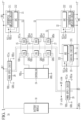
- FIG. 1 schematically illustrates a battery pack according to an embodiment.
- the battery pack 1a may include a plurality of pack terminals P+ and P-, a battery module 10, a plurality of switches SW1 and SW2, and a switch diagnosis device.
- the pack terminals P+ and P- may be connected to external devices (e.g., a load, a charger, etc.) of the battery pack 1a.
- the pack terminals P+ and P- may transfer discharge power supplied from the battery module 10 to a load or charge power applied from a charger to the battery module 10.
- the battery module 10 may include a plurality of cells connected in series and/or parallel to each other to provide a high voltage output.
- the switches SW1 and SW2 may be connected between the output terminals of the battery module 10 and the pack terminals P+ and P-, respectively.
- the switch SW1 may be connected between a positive output terminal of the battery module 10 and the positive pack terminal P+ to block or allow current flow between the two terminals.
- the switch SW2 may be connected between a negative output terminal of the battery module 10 and the negative pack terminal P- to block or allow current flow between the two terminals.
- the switches SW1 and SW2 may include a switching means that allows or blocks current flow through mechanical contact, using, e.g., a relay or a contactor.
- the switch diagnosis device may be further configured to detect the contact resistance of each of the switches SW1 and SW2, and to diagnose a deterioration state of each of the switches SW1 and SW2 based on the detected contact resistance.
- the switch diagnosis device may include a plurality of voltage sensing circuits 21 and 22, a current sensing circuit 23, and a controller 24.
- the voltage sensing circuits 21 and 22 may be connected to opposite ends of the respective switches SW1 and SW2 to detect voltages across the switches SW1 and SW2. Each of the voltage sensing circuits 21 and 22 may output voltage signals S1 and S2 in response to the detected voltages.
- the voltage sensing circuits 21 and 22 may respectively include differential amplifier circuits 211 and 221 and analog-to-digital converters (ADCs) 212 and 222.
- ADCs analog-to-digital converters
- the differential amplifier circuits 211 and 221 may be connected to opposite ends of the switches SW1 and SW2, respectively, and may respectively amplify and output voltages across the switches SW1 and SW2.
- Amplification gains of the differential amplification circuits 211 and 221 may be set in consideration of the contact resistance variation of the switch in a normal state, and they may be configured to have an amplification gain of 1 or more.
- the differential amplifier circuits 211 and 221 may be configured to have an amplification gain between 1 and 10.
- the differential amplification circuits 211 and 221 may be connected to bus bars (or contacts) constituting opposite ends of the corresponding switches SW1 and SW2 through a direct connection method through laser welding, etc., or an indirect connection method through wire harness, etc.
- the ADCs 212 and 222 may respectively convert analog signals outputted from the differential amplifier circuits 211 and 221 into digital voltage signals S1 and S2 to output the converted voltage signals S1 and S2.
- the current sensing circuit 23 may detect a current flowing in a high current path of the battery pack 1a through the switches SW1 and SW2.
- the current sensing circuit 23 may output a current signal S3 corresponding to the detected current.
- a 'high current path' is a current path between the battery module 10 and the pack terminals P+ and P-, and represents a path through which a charge or discharge current of the battery module 10 flows.
- the current sensing circuit 23 may include a shunt resistor, a hall sensor, a flux gate sensor, and the like.
- the current sensing circuit 23 may include a shunt resistor Rs and a sensing circuit 231 connected to opposite ends of the shunt resistor Rs to sense a current flowing through the shunt resistor Rs. Since a resistance value of the shunt resistor Rs is a fixed value, a voltage across the shunt resistor Rs may change in response to the current flowing through the shunt resistor Rs. Accordingly, the sensing circuit 231 may detect the current flowing through the shunt resistor Rs from the voltage across the shunt resistor Rs, and may output a signal corresponding to the detected current.
- the current sensing circuit 23 may further include an ADC 232 to convert an analog signal outputted from the sensing circuit 231 into a digital signal.
- the ADC 232 may convert the analog current signal outputted from the sensing circuit 231 into a digital current signal S3 to output it.
- the sensing circuit 231 may amplify the current signal with a predetermined amplification gain before outputting the current signal to the ADC 232 to output the current signal. Due to this amplification, even minute changes in current may be sensed, improving current sensing accuracy.
- An amplification gain of the sensing circuit 231 may be changed according to current specification of the battery pack 1a. That is, the sensing circuit 231 may be configured to be able to vary the amplification gain, and a value thereof may be determined according to the current specification of the battery pack 1a to which the switch diagnosis device is mounted.
- the sensing circuit 231 may be included in an analog front end (AFE) circuit of the battery pack 1a.
- AFE analog front end
- the controller 24 may respectively receive the voltage signals S1 and S2 corresponding to the voltages across the switches SW1 and SW2 from the voltage sensing circuits 21 and 22 of the switches SW1 and SW2. In addition, the controller 24 may receive the current signal S3 corresponding to the current flowing in the high current path of the battery pack 1a from the current sensing circuit 23 through the switches SW1 and SW2.
- the controller 24 may calculate contact resistance of each of the switches SW1 and SW2 based on the received voltage signals S1 and S2 and the current signal S3.
- the controller 24 may use the voltage signals S1 and S2 and the current signal S3 detected in the closed state of the switches SW1 and SW2 to calculate the contact resistance of the switches SW1 and SW2.
- the controller 24 may monitor the current flowing through the high current path of the battery pack 1a to check whether a current flow satisfies a specific condition, and may calculate the contact resistance of the switches SW1 and SW2 using the voltage signals S1 and S2 and the current signal S3 obtained in a state where the current flow satisfies the specific condition.
- the controller 24 may determine that an average current flowing through the high current path of the battery pack 1a during a predetermined period is within a predetermined range including an upper limit value and a lower limit value, and when a differential value (di/dt) of the current flowing through the high current path is below a predetermined value, may calculate the contact resistance of the switches SW1 and SW2 using the voltage signals S1 and S2 and the current signal S3 obtained during the corresponding period. In addition, for example, the controller 24 may calculate the contact resistance of the switches SW1 and SW2 by using the voltage signals S1 and S2 and the current signal S3 detected during a period in which the battery module 10 is being charged with a constant current by a current within a predetermined range.
- the controller 24 may diagnose a deterioration state of each of the switches SW1 and SW2 based on the calculated contact resistance. For example, the controller 24 may determine that the corresponding switches SW1 and SW2 are deteriorated when the contact resistance of the switches SW1 and SW2 is equal to or greater than a predetermined threshold. When it is determined that the switches SW1 and SW2 are deteriorated, the controller 24 may output a diagnosis signal warning of a deterioration state of the switches SW1 and SW2 to an upper controller (e.g., an electronic control unit (ECU) of an electric vehicle).
- ECU electronice control unit
- the controller 24 may be a controller constituting a battery management system (BMS) that manages an overall operation of the battery pack 1a.
- BMS battery management system
- the battery pack 1a may include a high voltage (HV) system (hereinafter, referred to as a high voltage side) including the battery module 10 which is a power source at the high voltage side and a low voltage (LV) system (hereinafter, referred to as a low voltage side) including the controller 24, and the low voltage system and the high voltage system may be galvanically isolated from each other.
- HV high voltage
- LV low voltage
- Galvanic Isolation refers to a circuit technique that allows two or more electrical circuits to communicate each other while blocking an unwanted DC current.
- Galvanic isolation may be implemented using magnetic induction, capacitance, optical signals, electromagnetic waves, or acoustic signals. Using galvanic isolation, it is possible to prevent formation of a communication path between systems having different reference potentials, or an unwanted current from flowing due to a ground loop.
- the voltage sensing circuits 21 and 22 and the current sensing circuit 23 are a high voltage component, unlike the controller 24, which is a low voltage component. Accordingly, it is necessary to construct a communication path using galvanic isolation in order to transfer the signals S1, S2 and S3 generated by the voltage sensing circuits 21 and 22 and the current sensing circuit 23 to the controller 24.
- the switch diagnosis device may further include a plurality of isolated communication circuits 25, 26, and 27.
- the isolated communication circuit 25 may receive the voltage signal S1 corresponding to the voltage across the switch SW1 from the voltage sensing circuit 21 at the high voltage side, and may transmit it to the controller 24 at the low voltage side through an isolated communication method.
- the isolated communication circuit 25 may include a high voltage sub-circuit 25H connected to the voltage sensing circuit 21 and a low voltage sub-circuit 25L connected to the controller 24.
- the high voltage sub-circuit 25H may receive the voltage signal S1 from the voltage sensing circuit 21, and may transmit it to the low voltage sub-circuit 25L in an isolated communication method.
- the low voltage sub-circuit 25L may transfer the voltage signal S1 transferred from the high voltage sub-circuit 25H through the isolated communication method to the controller 24.
- the isolated communication circuit 26 may receive the voltage signal S2 corresponding to the voltage across the switch SW2 from the voltage sensing circuit 22 at a high voltage side, and may transmit it to the controller 24 at a low voltage side through an isolated communication method.
- the isolated communication circuit 26 may include a high voltage sub-circuit 26H connected to the voltage sensing circuit 22 and a low voltage sub-circuit 26L connected to the controller 24.
- the high voltage sub-circuit 26H may receive the voltage signal S2 from the voltage sensing circuit 22, and may transmit it to the low voltage sub-circuit 26L in an isolated communication method.
- the low voltage sub-circuit 26L may transfer the voltage signal S2 transferred from the high voltage sub-circuit 26H through the isolated communication method to the controller 24.
- the isolation communication circuit 27 may receive the current signal S3 corresponding to the current flowing through the high current path from the current sensing circuit 23 at the high voltage side, and may transmit it to the controller 24 at the low voltage side in the isolated communication method.
- the isolated communication circuit 27 may include a high voltage sub-circuit 27H connected to the current sensing circuit 23 and a low voltage sub-circuit 27L connected to the controller 24.
- the high voltage sub-circuit 27H may receive the current signal S3 from the current sensing circuit 23, and may transmit it to the low voltage sub-circuit 27L in an isolated communication method.
- the low voltage sub-circuit 27L may transfer the current signal S3 transferred from the high voltage sub-circuit 27H through the isolated communication method to the controller 24.
- the isolated communication circuits 25, 26, and 27 may transfer signals between the low voltage side and the high voltage side in various communication methods such as a serial peripheral interface (SPI), an inter-integrated circuit (I2C), single edge nibble transmission (SENT), a controller area network (CAN), and the like.
- SPI serial peripheral interface
- I2C inter-integrated circuit
- SENT single edge nibble transmission
- CAN controller area network
- the battery pack 1a may further include power supply circuits 28 and 29 for supplying a driving voltage to the isolated communication circuits 25 and 26.
- the power supply circuit 28 may receive the supply voltage VDD L1 at the low voltage side, and may output a supply voltage VCC H1 at the high voltage side, converted therefrom.
- the power supply circuit 28 may include an isolated DC-DC converter (e.g., a flyback converter) including a primary side receiving the supply voltage VDD L1 at the low voltage side and a secondary side outputting the supply voltage VCC H1 at the high voltage side.
- a secondary circuit of the power supply circuit 28 may be connected to a node HV+ connected to a positive output terminal of the battery module 10, and may generate a reference potential VEE H1 of the supply voltage VCC H1 based on a potential of the node HV+.
- a reference potential of the supply voltage VCC H1 may be lower than the potential of the node HV+.
- the supply voltage VCC H1 outputted from the power supply circuit 28 may be supplied as a driving voltage for the differential amplifier circuit 211 and the ADC 212 of the voltage sensing circuit 21 and the high voltage sub-circuit 25H of the isolated communication circuit 25.
- the low voltage sub-circuit 25L of the isolated communication circuit 25 may operate using a supply voltage VDD L2 supplied from a low voltage power source (not illustrated) at the low voltage side as a driving voltage.
- the supply voltage VDD L2 may be used as a driving voltage of the controller 24.
- the power supply circuit 29 may receive the supply voltage VDD L1 at the low voltage side, and may output a supply voltage VCC H2 at the high voltage side, converted therefrom.
- the power supply circuit 29 may include an isolated DC-DC converter (e.g., a flyback converter) including a primary side receiving the supply voltage VDD L1 at the low voltage side and a secondary side outputting the supply voltage VCC H2 at the high voltage side.
- a secondary circuit of the power supply circuit 29 may be connected to a node HV- connected to a negative output terminal of the battery module 10, and may generate a reference potential VEE H2 of the supply voltage VCC H2 based on a potential of the node HV-.
- a reference potential of the supply voltage VCC H2 may be lower than the potential of the node HV-.
- the supply voltage VCC H2 outputted from the power supply circuit 29 may be supplied as a driving voltage for the differential amplifier circuit 221 and the ADC 222 of the voltage sensing circuit 22 and the high voltage sub-circuit 26H of the isolated communication circuit 26.
- the low voltage sub-circuit 26L of the isolated communication circuit 25 may operate using a supply voltage VDD L2 supplied from a low voltage power source (not illustrated) at the low voltage side as a driving voltage.
- the supply voltage VDD L1 at the low voltage side inputted to the power supply circuits 28 and 29 may be a voltage supplied from an outside of the battery pack 1a (e.g., a vehicle) in order to minimize power consumption of the battery pack 1a.
- the present embodiment is not limited thereto, and the supply voltage VDD L1 at the low voltage side inputted to the power supply circuits 28 and 29 may be a voltage supplied from a low voltage power source (not illustrated) positioned inside the battery pack 1a.
- the supply voltage VDD L1 may be a voltage supplied from the same low voltage power source as the supply voltage VDD L2 at the low voltage side, used as a driving voltage of the controller 24.
- the sensing circuit 231 and the ADC 232 of the current sensing circuit 23 and the high voltage sub-circuit 27H of the isolated communication circuit 27 may be driven by a supply voltage VCC H3 at the high voltage side with a ground potential GND H at the high voltage side as a reference potential.
- the supply voltage VCC H3 may be a voltage converted from the battery module 10 or a low voltage power source(not illustrated) at the low voltage side through a separate power supply circuit (not illustrated).
- the supply voltage VCC H3 may be a voltage converted from the above-described supply voltage VCC H1 or supply voltage VCC H2 .
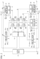
- FIG. 2 schematically illustrates a control server of a battery pack according to another embodiment.
- the battery pack 1b may further include temperature sensors 31 and 32 compared to the battery pack 1a described with reference to FIG. 1 .
- Each of the temperature sensors 31 and 32 may detect the temperature of each of the switches SW1 and SW2 to output temperature signals S4 and S5.
- Each of the temperature sensors 31 and 32 may be positioned in contact with or adjacent to bus bars (or contacts) constituting opposite ends of the corresponding switch SW1 or SW2 for temperature measurement.
- the controller 24 may receive the temperature signals S4 and S5 corresponding to the temperatures of the respective switches SW1 and SW2 from the temperature sensors 31 and 32. When the temperature signals S4 and S5 are received, the controller 24 may increase diagnosis coverage by using contact resistance of each of the switches SW1 and SW2 to diagnose deterioration states of the switches SW1 and SW2. For example, the controller 24 may determine that the switches SW1 and SW2 are in a deteriorated state or in a welded state when the temperatures of the switches SW1 and SW2 indicated by the temperature signals S4 and S5 are higher than a predetermined threshold.
- the battery packs 1a and 1b may calculate the contact resistance of the switches SW1 and SW2 using the voltage and current across the switches SW1 and SW2 directly sensed through the switch diagnosis device.
- the battery packs 1a and 1b also diagnose the deterioration state of the switches SW1 and SW2 from the contact resistance of the switches SW1 and SW2 calculated in this way, so that preemptive measures such as parts replacement are possible before welding occurs.
- An electronic or electrical device and/or any other related device or component according to the embodiments of the present disclosure described herein may be implemented by using any suitable hardware, firmware (e.g., an application-specific integrated circuit), software, or a combination of software, firmware, and hardware.
- various components of these devices may be disposed on one integrated circuit (IC) chip or on separate IC chips.
- various components of these devices may be implemented on a flexible printed circuit film (TCP), a tape carrier package (TCP), a printed circuit board (PCB), or on one substrate.
- TCP flexible printed circuit film
- TCP tape carrier package
- PCB printed circuit board
- the electrical connections or interconnections described in the present specification may be implemented by wires or conductive elements, e.g., on a PCB or on other types of circuit carriers.
- the conductive element may include, e.g., metallization, such as surface metallization, and/or pins, and may include conductive polymers or ceramics. Electrical energy may also be transmitted via a wireless connection using, e.g., electromagnetic radiation or light.
- various components of these devices may be executed on one or more processors to perform various functions described herein and within one or more computing devices, and may be processes or threads that execute computer program instructions and may interact with other system components.
- Computer program instructions are stored in a memory that can be implemented in a computing device using a standard memory device, such as, e.g., a random access memory (RAM).
- the computer program instructions may also be stored on other non-transitory computer readable media, e.g., CD-ROMs, flash drives, and the like.
Landscapes
- General Physics & Mathematics (AREA)
- Physics & Mathematics (AREA)
- Engineering & Computer Science (AREA)
- Chemical & Material Sciences (AREA)
- General Chemical & Material Sciences (AREA)
- Electrochemistry (AREA)
- Chemical Kinetics & Catalysis (AREA)
- Manufacturing & Machinery (AREA)
- Power Engineering (AREA)
- Theoretical Computer Science (AREA)
- Computer Networks & Wireless Communication (AREA)
- Microelectronics & Electronic Packaging (AREA)
- Secondary Cells (AREA)
- Charge And Discharge Circuits For Batteries Or The Like (AREA)
Abstract
An embodiment provides a switch diagnosis device including: a switch positioned in a current path at a high voltage side; a voltage sensing circuit configured to generate a voltage signal by sensing a voltage across the switch at the high voltage side; a current sensing circuit configured to generate a current signal by detecting a current flowing through the current path; a controller configured to receive the voltage signal and the current signal, to calculate contact resistance of the switch based on the received voltage signal and the received current signal, and to diagnose a deterioration state of the switch based on the calculated contact resistance; and a first isolated communication circuit configured to transfer the voltage signal outputted from the voltage sensing circuit to the controller at a low voltage side that is galvanically isolated from the high voltage side.
Description
- The present disclosure relates to a switch diagnosis device and a battery pack including the same.
- A rechargeable or secondary battery differs from a primary battery in that charging and discharging can be repeated, and the primary battery only provides non-reversible conversion from chemical energy to electrical energy. A low-capacity rechargeable battery is used as a power supply device for small electronic devices such as portable telephones, laptops computers, and camcorders, and a high-capacity rechargeable battery is used as a power supply device for an energy storage system (ESS) or uninterruptible power supply (UPS) using medium or large batteries used for electric vehicles (EVs), hybrid vehicles (HVs), for home or industry system, etc.
- In general, the secondary battery may include an electrode assembly including a positive electrode, a negative electrode, and a separator interposed between the positive electrode and the negative electrode, a case for accommodating the electrode assembly therein, and an electrode terminal electrically connected to the electrode assembly. An electrolyte solution is injected into the case to enable charging and discharging of the battery through an electrochemical reaction of the positive electrode, the negative electrode, and the electrolyte solution. A shape of the case, such as cylindrical or rectangular, depends on an application of the battery.
- The rechargeable battery is used in the form of a battery module including a plurality of unit battery cells connected in series and/or in parallel, thereby providing high energy density for running, e.g., a hybrid vehicle. That is, the battery module is formed by interconnecting electrode terminals of a plurality of unit battery cells according to an amount of power required to implement a high-power rechargeable battery for an electric vehicle, for example. One or more battery modules are mechanically and electrically integrated to form a battery pack.
- In a high voltage battery pack mounted in an electric vehicle or the like, a mechanical relay is mainly used as a switching means for opening and closing a high current path between the battery pack and an external device (load or charger). The mechanical relay has a disadvantage of being heavy and bulky and high current consumption of the secondary coil for control, and has an advantage in that energy loss of the battery pack can be minimized due to a characteristic having large insulation resistance (receiving Mohm) when a high current path is blocked.
- The mechanical relay has a structure in which bus bars are mechanically connected by a magnetic force induced by a secondary side coil. In mechanical relays having such a structure, defects due to welding are continuously identified. In a process of repeating contact between bus bars constituting a relay, a direct contact current path between the bus bars is narrowed due to foreign matters plating peeling, and irregularities, and due to a phenomenon of current concentration to the local portion caused thereby, heat generation and contact resistance increase may occur, leading to defects such as welding.
- When the coupling state between the bus bars is maintained due to welding, a high current path of the high voltage pack may not be blocked, which may cause a safety accident. Accordingly, in order to prevent an accident due to welding of a relay, methods for diagnosing welding occurrence using a voltage across a bus bar constituting the relay have been proposed. Such methods are useful only when the relay is out of order because it can only diagnose whether or not the relay is out of order, and there is a problem in that it is impossible to predict a failure of the relay in advance and deal with it preemptively.
- Embodiments attempt to provide a switch diagnosis device, and a battery pack including the same, capable of predicting a failure of a relay in advance such that preemptive measures can be taken before the failure of the relay.
- An embodiment of the present disclosure provides a switch diagnosis device including: a switch positioned in a current path at a high voltage side; a voltage sensing circuit configured to generate a voltage signal by sensing a voltage across the switch at the high voltage side; a current sensing circuit configured to generate a current signal by detecting a current flowing through the current path; a controller configured to receive the voltage signal and the current signal, to calculate contact resistance of the switch based on the received voltage signal and the received current signal, and to diagnose a deterioration state of the switch based on the calculated contact resistance; and a first isolated communication circuit configured to transfer the voltage signal outputted from the voltage sensing circuit to the controller at a low voltage side that is galvanically isolated from the high voltage side.
- The first isolated communication circuit may include: a first sub-circuit configured to transmit the voltage signal received from the voltage sensing circuit at the high voltage side to at low voltage in an isolated communication method; and a second sub-circuit configured to transmit the voltage signal received from the first sub-circuit at the high voltage side to the controller at the low voltage.
- The switch diagnosis device may further include a power supply circuit configured to supply a supply voltage for driving the voltage sensing circuit and the first sub-circuit.
- The power supply circuit may be connected to a node between a power source at the high voltage side and the switch, and configured to determine a reference potential of the supply voltage based on a potential of the node.
- The power supply circuit may include an isolated DC-DC converter configured to generates the supply voltage from a voltage inputted from the low voltage side.
- The isolated DC-DC converter may be a flyback converter.
- The voltage sensing circuit may include: a differential amplifier circuit connected to opposite ends of the switch; and an analog-to-digital converter configured to generate the voltage signal, which is a digital signal, from an output signal of the differential amplifier circuit.
- The current sensing circuit may include: a shunt resistor connected to the current path; a sensing circuit configured to output a signal corresponding to a current flowing through the switch from a voltage across the shunt resistor; and an analog-to-digital converter configured to generate the current signal, which is a digital signal, from a signal output from the sensing circuit.
- The switch diagnosis device may further include a second isolated communication circuit configured to transfer the current signal outputted from the current sensing circuit to the controller at a low voltage side that is galvanically isolated from the high voltage side.
- The controller may be further configured to calculate the contact resistance using the voltage signal and the current signal obtained by sensing a voltage across the switch and a current flowing through the switch during a period in which the current flowing through the current path in a state in which the switch is closed satisfies a specific condition.
- The controller may be further configured to determine that the specific condition is satisfied when the current flowing through the current path is within a predetermined range and a differential value of the current flowing through the current path is within a predetermined value.
- The switch may be a relay or a contactor.
- An embodiment of the present disclosure provides a battery pack including: a plurality of pack terminals; a battery module configured to include a plurality of cells connected in series or parallel to each other between the pack terminals; a first switch connected between a first output terminal of the battery module and a first pack terminal among the pack terminals at the high voltage side, and opening and closing a current path between the pack terminals and the battery module; a first voltage sensing circuit configured to generate a first voltage signal by sensing a voltage across the first switch at the high voltage side; a current sensing circuit configured to generate a current signal by detecting a current flowing through the current path; a controller configured to receive the first voltage signal and the current signal, to calculate first contact resistance of the first switch based on the received first voltage signal and the received current signal, and to diagnose a deterioration state of the first switch based on the calculated first contact resistance; and a first isolated communication circuit configured to transfer the first voltage signal outputted from the first voltage sensing circuit to the controller at a low voltage side that is galvanically isolated from the high voltage side.
- The first isolated communication circuit may include: a first high voltage sub-circuit configured to transmit the first voltage signal received from the first voltage sensing circuit at the high voltage side in an isolated communication method; and a first low voltage sub-circuit configured to transmit the first voltage signal received from the first high voltage sub-circuit to the controller at the low voltage side.
- The battery pack may further include a first power supply circuit configured to supply a first supply voltage for driving the first voltage sensing circuit and the first high voltage sub-circuit.
- The first power supply circuit may be configured such that a reference potential of the first supply voltage is determined based on a potential of the first output terminal.
- The power supply circuit may include an isolated DC-DC converter configured to generates the first supply voltage from a voltage inputted from the low voltage side.
- The voltage inputted from the low voltage side to the first power supply circuit may be a supply voltage supplied from a vehicle equipped with the battery pack.
- The battery pack may further include: a second switch connected between a second output terminal of the battery module and a second pack terminal among the pack terminals and configured to open and close the current path; a second voltage sensing circuit configured to generate a second voltage signal by sensing a voltage across the second switch at the high voltage side; and a second isolated communication circuit configured to transmit the second voltage signal outputted from the second voltage sensing circuit to the controller at the low voltage side.
- The controller may be further configured to calculate second contact resistance of the second switch based on the received second voltage signal and the received current signal, and to diagnose a deterioration state of the second switch based on the calculated second contact resistance.
- The second isolated communication circuit may include: a second high voltage sub-circuit configured to transmit the second voltage signal received from the second voltage sensing circuit at the high voltage side in an isolated communication method; and a second low voltage sub-circuit configured to transmit the second voltage signal received from the second high voltage sub-circuit to the controller at the low voltage side.
- The battery pack may further include a second power supply circuit configured to supply a second supply voltage for driving the second voltage sensing circuit and the second high voltage sub-circuit.
- The second power supply circuit may be configured such that a reference potential of the second supply voltage is determined based on a potential of the second output terminal.
- The first voltage sensing circuit may include: a differential amplifier circuit connected to opposite ends of the first switch; and an analog-to-digital converter configured to generate the first voltage signal, which is a digital signal, from an output signal of the differential amplifier circuit.
- The battery pack may further include a second isolated communication circuit configured to transfer the current signal outputted from the current sensing circuit to the controller at a low voltage side that is galvanically isolated from the high voltage side.
- The current sensing circuit may include a shunt resistor connected to the current path; a sensing circuit configured to output a signal corresponding to the current flowing through the current path from a voltage across the shunt resistor; and an analog-to-digital converter configured to generate the current signal, which is a digital signal, from a signal output from the sensing circuit.
- The controller may be further configured to calculate the first contact resistance using the first voltage signal and the current signal obtained by sensing a voltage across the first switch and a current flowing through the first switch during a period in which the current flowing through the current path in a state in which the first switch is closed satisfies a specific condition.
- The controller may be further configured to determine that the specific condition is satisfied when the current flowing through the current path is within a predetermined range and a differential value of the current flowing through the current path is within a predetermined value.
- The first switch may be a relay or a contactor.
- The battery pack may further include a temperature sensor configured to sense a temperature of the first switch.
- The controller may be further configured to diagnose a deterioration state of the first switch based on a temperature signal received from the temperature sensor and the first contact resistance.
- At least some of the above and other features of the invention are set out in the claims.
- According to the embodiments, it is possible to preemptively cope with a failure of a relay by predicting the failure of the relay in advance.
-
-
FIG. 1 schematically illustrates a battery pack according to an embodiment. -
FIG. 2 schematically illustrates a control server of a battery pack according to another embodiment. - Embodiments of the present disclosure will now be described in detail with reference to the accompanying drawings. Hereinafter, an operation effect and a method of implementing the same according to embodiments of the present disclosure will be described with reference to the accompanying drawings. In the drawings, the same reference numerals denote the same elements, and redundant explanations will be omitted. However, the present disclosure may be embodied in various forms, and should not be construed as being limited only to the embodiments shown herein. Rather, these embodiments are provided by way of example to make the present disclosure thorough and complete, and will fully convey aspects and features of the present disclosure to those skilled in the art.
- Accordingly, processes, elements, and techniques deemed not necessary to those skilled in the art for complete understanding of aspects and features of the disclosure may not be described. In the drawings, the relative sizes of elements, layers, and regions may be exaggerated for clarity.
- As used herein, the term "and/or" includes any and all combinations of one or more related listed items. The use of "can/may" in describing an embodiment of the present disclosure indicates "at least one embodiment of the present disclosure."
- In the following description of embodiments of the present disclosure, terms in the singular form may include plural forms unless the context clearly indicates otherwise.
- It will be understood that terms including ordinal numbers such as "first", "second", "third", etc. are used to describe various elements, but these elements should not be limited by these terms. These terms are only used to distinguish one element from another. For example, a first constituent element may be referred to as a second constituent element, and the second constituent element may be referred to as the first constituent element without departing from the scope of the present disclosure. As used herein, the term "and/or" includes any and all combinations of one or more related listed items. An expression such as "at least one" precedes a list of elements, modifying the entire list of elements and not individual elements of the list.
- As used in this specification, the terms "substantially", "approximately", and similar terms are used as approximate terms but are not used as degree terms, and they are not intended to illustrate inherent deviations of measured or calculated values evident to those skilled in the art. In addition, when the term "substantially" is used in combination with a characteristic that can be expressed using numerical values, the term "substantially" refers to including a range of +/- 5 % of the value.
- When one component or layer is described as "on", "connected to", or "coupled" to another component or layer, "on", "connected to" and "coupled to" "Includes those formed directly or through the intervening of one or more other components or layers. In addition, when one component or layer is described as being "between" two components or layers, it should be understood that it is the only component or layer between two components or layers, or that there are one or more intervening other components or layers.
- A case of electrically connecting two constituent elements includes not only a case of directly connecting the constituent elements but also a case of connecting the constituent elements via another constituent element therebetween. The constituent element therebetween may include a switch, a resistor, a capacitor, and the like. In describing embodiments, an expression of connection indicates electrical connection unless explicitly described to be direct connection.
-
FIG. 1 schematically illustrates a battery pack according to an embodiment. - Referring to
FIG. 1 , the battery pack 1a according to an embodiment may include a plurality of pack terminals P+ and P-, abattery module 10, a plurality of switches SW1 and SW2, and a switch diagnosis device. - The pack terminals P+ and P- may be connected to external devices (e.g., a load, a charger, etc.) of the battery pack 1a. The pack terminals P+ and P- may transfer discharge power supplied from the
battery module 10 to a load or charge power applied from a charger to thebattery module 10. - The
battery module 10 may include a plurality of cells connected in series and/or parallel to each other to provide a high voltage output. - The switches SW1 and SW2 may be connected between the output terminals of the
battery module 10 and the pack terminals P+ and P-, respectively. The switch SW1 may be connected between a positive output terminal of thebattery module 10 and the positive pack terminal P+ to block or allow current flow between the two terminals. The switch SW2 may be connected between a negative output terminal of thebattery module 10 and the negative pack terminal P- to block or allow current flow between the two terminals. - The switches SW1 and SW2 may include a switching means that allows or blocks current flow through mechanical contact, using, e.g., a relay or a contactor.
- The switch diagnosis device may be further configured to detect the contact resistance of each of the switches SW1 and SW2, and to diagnose a deterioration state of each of the switches SW1 and SW2 based on the detected contact resistance. To this end, the switch diagnosis device may include a plurality of
voltage sensing circuits current sensing circuit 23, and acontroller 24. - The
voltage sensing circuits voltage sensing circuits - The
voltage sensing circuits differential amplifier circuits - The
differential amplifier circuits differential amplification circuits differential amplifier circuits - The
differential amplification circuits - The
ADCs differential amplifier circuits - The
current sensing circuit 23 may detect a current flowing in a high current path of the battery pack 1a through the switches SW1 and SW2. Thecurrent sensing circuit 23 may output a current signal S3 corresponding to the detected current. In this document, a 'high current path' is a current path between thebattery module 10 and the pack terminals P+ and P-, and represents a path through which a charge or discharge current of thebattery module 10 flows. - The
current sensing circuit 23 may include a shunt resistor, a hall sensor, a flux gate sensor, and the like. - Referring to
FIG. 1 as an example, thecurrent sensing circuit 23 may include a shunt resistor Rs and asensing circuit 231 connected to opposite ends of the shunt resistor Rs to sense a current flowing through the shunt resistor Rs. Since a resistance value of the shunt resistor Rs is a fixed value, a voltage across the shunt resistor Rs may change in response to the current flowing through the shunt resistor Rs. Accordingly, thesensing circuit 231 may detect the current flowing through the shunt resistor Rs from the voltage across the shunt resistor Rs, and may output a signal corresponding to the detected current. - The
current sensing circuit 23 may further include anADC 232 to convert an analog signal outputted from thesensing circuit 231 into a digital signal. TheADC 232 may convert the analog current signal outputted from thesensing circuit 231 into a digital current signal S3 to output it. - Meanwhile, the
sensing circuit 231 may amplify the current signal with a predetermined amplification gain before outputting the current signal to theADC 232 to output the current signal. Due to this amplification, even minute changes in current may be sensed, improving current sensing accuracy. An amplification gain of thesensing circuit 231 may be changed according to current specification of the battery pack 1a. That is, thesensing circuit 231 may be configured to be able to vary the amplification gain, and a value thereof may be determined according to the current specification of the battery pack 1a to which the switch diagnosis device is mounted. - The
sensing circuit 231 may be included in an analog front end (AFE) circuit of the battery pack 1a. - The
controller 24 may respectively receive the voltage signals S1 and S2 corresponding to the voltages across the switches SW1 and SW2 from thevoltage sensing circuits controller 24 may receive the current signal S3 corresponding to the current flowing in the high current path of the battery pack 1a from thecurrent sensing circuit 23 through the switches SW1 and SW2. - The
controller 24 may calculate contact resistance of each of the switches SW1 and SW2 based on the received voltage signals S1 and S2 and the current signal S3. - In order to calculate the contact resistance of each of the switches SW1 and SW2, it is necessary to detect a voltage and current across each of the switches SW1 and SW2 in a closed state. Accordingly, the
controller 24 may use the voltage signals S1 and S2 and the current signal S3 detected in the closed state of the switches SW1 and SW2 to calculate the contact resistance of the switches SW1 and SW2. - When the current flowing through the high current path of the battery pack 1a changes rapidly, a sensing error occurs due to a phase difference between voltage and current sensing values, which may decrease accuracy of the contact resistance. In addition, during a period in which a direction of the current flowing through the high current path of the battery pack 1a is changed, there may be a period in which the contact resistance is instantaneously detected as infinite, and when the current flowing through the high current path is low, the sensing error may increase and the accuracy of the contact resistance may also decrease. Accordingly, the
controller 24 may monitor the current flowing through the high current path of the battery pack 1a to check whether a current flow satisfies a specific condition, and may calculate the contact resistance of the switches SW1 and SW2 using the voltage signals S1 and S2 and the current signal S3 obtained in a state where the current flow satisfies the specific condition. For example, thecontroller 24 may determine that an average current flowing through the high current path of the battery pack 1a during a predetermined period is within a predetermined range including an upper limit value and a lower limit value, and when a differential value (di/dt) of the current flowing through the high current path is below a predetermined value, may calculate the contact resistance of the switches SW1 and SW2 using the voltage signals S1 and S2 and the current signal S3 obtained during the corresponding period. In addition, for example, thecontroller 24 may calculate the contact resistance of the switches SW1 and SW2 by using the voltage signals S1 and S2 and the current signal S3 detected during a period in which thebattery module 10 is being charged with a constant current by a current within a predetermined range. - When the contact resistance of each of the switches SW1 and SW2 is calculated, the
controller 24 may diagnose a deterioration state of each of the switches SW1 and SW2 based on the calculated contact resistance. For example, thecontroller 24 may determine that the corresponding switches SW1 and SW2 are deteriorated when the contact resistance of the switches SW1 and SW2 is equal to or greater than a predetermined threshold. When it is determined that the switches SW1 and SW2 are deteriorated, thecontroller 24 may output a diagnosis signal warning of a deterioration state of the switches SW1 and SW2 to an upper controller (e.g., an electronic control unit (ECU) of an electric vehicle). - The
controller 24 may be a controller constituting a battery management system (BMS) that manages an overall operation of the battery pack 1a. - The battery pack 1a may include a high voltage (HV) system (hereinafter, referred to as a high voltage side) including the
battery module 10 which is a power source at the high voltage side and a low voltage (LV) system (hereinafter, referred to as a low voltage side) including thecontroller 24, and the low voltage system and the high voltage system may be galvanically isolated from each other. Galvanic Isolation refers to a circuit technique that allows two or more electrical circuits to communicate each other while blocking an unwanted DC current. Galvanic isolation may be implemented using magnetic induction, capacitance, optical signals, electromagnetic waves, or acoustic signals. Using galvanic isolation, it is possible to prevent formation of a communication path between systems having different reference potentials, or an unwanted current from flowing due to a ground loop. - Meanwhile, the
voltage sensing circuits current sensing circuit 23 are a high voltage component, unlike thecontroller 24, which is a low voltage component. Accordingly, it is necessary to construct a communication path using galvanic isolation in order to transfer the signals S1, S2 and S3 generated by thevoltage sensing circuits current sensing circuit 23 to thecontroller 24. To this end, the switch diagnosis device may further include a plurality ofisolated communication circuits - The
isolated communication circuit 25 may receive the voltage signal S1 corresponding to the voltage across the switch SW1 from thevoltage sensing circuit 21 at the high voltage side, and may transmit it to thecontroller 24 at the low voltage side through an isolated communication method. Theisolated communication circuit 25 may include ahigh voltage sub-circuit 25H connected to thevoltage sensing circuit 21 and alow voltage sub-circuit 25L connected to thecontroller 24. Thehigh voltage sub-circuit 25H may receive the voltage signal S1 from thevoltage sensing circuit 21, and may transmit it to thelow voltage sub-circuit 25L in an isolated communication method. Thelow voltage sub-circuit 25L may transfer the voltage signal S1 transferred from thehigh voltage sub-circuit 25H through the isolated communication method to thecontroller 24. - The
isolated communication circuit 26 may receive the voltage signal S2 corresponding to the voltage across the switch SW2 from thevoltage sensing circuit 22 at a high voltage side, and may transmit it to thecontroller 24 at a low voltage side through an isolated communication method. Theisolated communication circuit 26 may include ahigh voltage sub-circuit 26H connected to thevoltage sensing circuit 22 and alow voltage sub-circuit 26L connected to thecontroller 24. Thehigh voltage sub-circuit 26H may receive the voltage signal S2 from thevoltage sensing circuit 22, and may transmit it to thelow voltage sub-circuit 26L in an isolated communication method. Thelow voltage sub-circuit 26L may transfer the voltage signal S2 transferred from thehigh voltage sub-circuit 26H through the isolated communication method to thecontroller 24. - The
isolation communication circuit 27 may receive the current signal S3 corresponding to the current flowing through the high current path from thecurrent sensing circuit 23 at the high voltage side, and may transmit it to thecontroller 24 at the low voltage side in the isolated communication method. Theisolated communication circuit 27 may include ahigh voltage sub-circuit 27H connected to thecurrent sensing circuit 23 and alow voltage sub-circuit 27L connected to thecontroller 24. Thehigh voltage sub-circuit 27H may receive the current signal S3 from thecurrent sensing circuit 23, and may transmit it to thelow voltage sub-circuit 27L in an isolated communication method. Thelow voltage sub-circuit 27L may transfer the current signal S3 transferred from thehigh voltage sub-circuit 27H through the isolated communication method to thecontroller 24. - The
isolated communication circuits - The battery pack 1a may further include
power supply circuits isolated communication circuits - The
power supply circuit 28 may receive the supply voltage VDDL1 at the low voltage side, and may output a supply voltage VCCH1 at the high voltage side, converted therefrom. Thepower supply circuit 28 may include an isolated DC-DC converter (e.g., a flyback converter) including a primary side receiving the supply voltage VDDL1 at the low voltage side and a secondary side outputting the supply voltage VCCH1 at the high voltage side. A secondary circuit of thepower supply circuit 28 may be connected to a node HV+ connected to a positive output terminal of thebattery module 10, and may generate a reference potential VEEH1 of the supply voltage VCCH1 based on a potential of the node HV+. A reference potential of the supply voltage VCCH1 may be lower than the potential of the node HV+. - The supply voltage VCCH1 outputted from the
power supply circuit 28 may be supplied as a driving voltage for thedifferential amplifier circuit 211 and theADC 212 of thevoltage sensing circuit 21 and thehigh voltage sub-circuit 25H of theisolated communication circuit 25. Thelow voltage sub-circuit 25L of theisolated communication circuit 25 may operate using a supply voltage VDDL2 supplied from a low voltage power source (not illustrated) at the low voltage side as a driving voltage. The supply voltage VDDL2 may be used as a driving voltage of thecontroller 24. - The
power supply circuit 29 may receive the supply voltage VDDL1 at the low voltage side, and may output a supply voltage VCCH2 at the high voltage side, converted therefrom. Thepower supply circuit 29 may include an isolated DC-DC converter (e.g., a flyback converter) including a primary side receiving the supply voltage VDDL1 at the low voltage side and a secondary side outputting the supply voltage VCCH2 at the high voltage side. A secondary circuit of thepower supply circuit 29 may be connected to a node HV- connected to a negative output terminal of thebattery module 10, and may generate a reference potential VEEH2 of the supply voltage VCCH2 based on a potential of the node HV-. A reference potential of the supply voltage VCCH2 may be lower than the potential of the node HV-. - The supply voltage VCCH2 outputted from the
power supply circuit 29 may be supplied as a driving voltage for thedifferential amplifier circuit 221 and theADC 222 of thevoltage sensing circuit 22 and thehigh voltage sub-circuit 26H of theisolated communication circuit 26. Thelow voltage sub-circuit 26L of theisolated communication circuit 25 may operate using a supply voltage VDDL2 supplied from a low voltage power source (not illustrated) at the low voltage side as a driving voltage. - The supply voltage VDDL1 at the low voltage side inputted to the
power supply circuits power supply circuits controller 24. - The
sensing circuit 231 and theADC 232 of thecurrent sensing circuit 23 and thehigh voltage sub-circuit 27H of theisolated communication circuit 27 may be driven by a supply voltage VCCH3 at the high voltage side with a ground potential GNDH at the high voltage side as a reference potential. The supply voltage VCCH3 may be a voltage converted from thebattery module 10 or a low voltage power source(not illustrated) at the low voltage side through a separate power supply circuit (not illustrated). The supply voltage VCCH3 may be a voltage converted from the above-described supply voltage VCCH1 or supply voltage VCCH2. -
FIG. 2 schematically illustrates a control server of a battery pack according to another embodiment. - Referring to
FIG. 2 , thebattery pack 1b according to another embodiment may further includetemperature sensors FIG. 1 . - Each of the
temperature sensors temperature sensors - The
controller 24 may receive the temperature signals S4 and S5 corresponding to the temperatures of the respective switches SW1 and SW2 from thetemperature sensors controller 24 may increase diagnosis coverage by using contact resistance of each of the switches SW1 and SW2 to diagnose deterioration states of the switches SW1 and SW2. For example, thecontroller 24 may determine that the switches SW1 and SW2 are in a deteriorated state or in a welded state when the temperatures of the switches SW1 and SW2 indicated by the temperature signals S4 and S5 are higher than a predetermined threshold. - According to the embodiments described above, the battery packs 1a and 1b may calculate the contact resistance of the switches SW1 and SW2 using the voltage and current across the switches SW1 and SW2 directly sensed through the switch diagnosis device. The battery packs 1a and 1b also diagnose the deterioration state of the switches SW1 and SW2 from the contact resistance of the switches SW1 and SW2 calculated in this way, so that preemptive measures such as parts replacement are possible before welding occurs.
- An electronic or electrical device and/or any other related device or component according to the embodiments of the present disclosure described herein may be implemented by using any suitable hardware, firmware (e.g., an application-specific integrated circuit), software, or a combination of software, firmware, and hardware. For example, various components of these devices may be disposed on one integrated circuit (IC) chip or on separate IC chips. In addition, various components of these devices may be implemented on a flexible printed circuit film (TCP), a tape carrier package (TCP), a printed circuit board (PCB), or on one substrate. The electrical connections or interconnections described in the present specification may be implemented by wires or conductive elements, e.g., on a PCB or on other types of circuit carriers. The conductive element may include, e.g., metallization, such as surface metallization, and/or pins, and may include conductive polymers or ceramics. Electrical energy may also be transmitted via a wireless connection using, e.g., electromagnetic radiation or light.
- In addition, various components of these devices may be executed on one or more processors to perform various functions described herein and within one or more computing devices, and may be processes or threads that execute computer program instructions and may interact with other system components. Computer program instructions are stored in a memory that can be implemented in a computing device using a standard memory device, such as, e.g., a random access memory (RAM). The computer program instructions may also be stored on other non-transitory computer readable media, e.g., CD-ROMs, flash drives, and the like.
- In addition, those skilled in the art should recognize that the functions of various computing devices may be combined or integrated into a single computing device, or a function of a particular computing device may be distributed across one or more other computing devices without departing from the scope of embodiments of the present disclosure.
- The inventive concept may include one or more of the following numbered embodiments:
- 1. A switch diagnosis device comprising: a switch positioned in a current path at a high voltage side; a voltage sensing circuit configured to generate a voltage signal by sensing a voltage across the switch at the high voltage side; a current sensing circuit configured to generate a current signal by detecting a current flowing through the current path; a controller configured to receive the voltage signal and the current signal, to calculate contact resistance of the switch based on the received voltage signal and the received current signal, and to diagnose a deterioration state of the switch based on the calculated contact resistance; and a first isolated communication circuit configured to transfer the voltage signal outputted from the voltage sensing circuit to the controller at a low voltage side that is galvanically isolated from the high voltage side.
- 2. The switch diagnosis device of
embodiment 1, wherein the first isolated communication circuit includes: a first sub-circuit configured to transmit the voltage signal received from the voltage sensing circuit at the high voltage side in an isolated communication method; and a second sub-circuit configured to transmit the voltage signal received from the first sub-circuit at the low voltage side to the controller. - 3. The switch diagnosis device of
embodiment 2, further comprising a power supply circuit configured to supply a supply voltage for driving the voltage sensing circuit and the first sub-circuit, wherein the power supply circuit is connected to a node between a power source at the high voltage side and the switch, and configured to determine a reference potential of the supply voltage based on a potential of the node. - 4. The switch diagnosis device of
embodiment 3, wherein the power supply circuit includes an isolated DC-DC converter configured to generates the supply voltage from a voltage inputted from the low voltage side. - 5. The switch diagnosis device of
embodiment 4, wherein the isolated DC-DC converter is a flyback converter. - 6. The switch diagnosis device of
embodiment 1, wherein the voltage sensing circuit includes: a differential amplifier circuit connected to opposite ends of the switch; and an analog-to-digital converter configured to generate the voltage signal, which is a digital signal, from an output signal of the differential amplifier circuit. - 7. The switch diagnosis device of
embodiment 1, wherein the current sensing circuit includes: a shunt resistor connected to the current path; a sensing circuit configured to output a signal corresponding to a current flowing through the switch from a voltage across the shunt resistor; and an analog-to-digital converter configured to generate the current signal, which is a digital signal, from a signal output from the sensing circuit. - 8. The switch diagnosis device of embodiment 7, further comprising a second isolated communication circuit configured to transfer the current signal outputted from the current sensing circuit to the controller at a low voltage side that is galvanically isolated from the high voltage side.
- 9. The switch diagnosis device of
embodiment 1, wherein the controller is further configured to calculate the contact resistance using the voltage signal and the current signal obtained by sensing a voltage across the switch and a current flowing through the switch during a period in which the current flowing through the current path in a state in which the switch is closed satisfies a specific condition. - 10. The switch diagnosis device of embodiment 9, wherein the controller is further configured to determine that the specific condition is satisfied when the current flowing through the current path is within a predetermined range and a differential value of the current flowing through the current path is within a predetermined value.
- 11. The switch diagnosis device of
embodiment 1, wherein the switch is a relay or a contactor. - 12. A battery pack comprising: a plurality of pack terminals; a battery module configured to include a plurality of cells connected in series or parallel to each other between the pack terminals; a first switch connected between a first output terminal of the battery module and a first pack terminal among the pack terminals at the high voltage side, and opening and closing a current path between the pack terminals and the battery module; a first voltage sensing circuit configured to generate a first voltage signal by sensing a voltage across the first switch at the high voltage side; a current sensing circuit configured to generate a current signal by detecting a current flowing through the current path; a controller configured to receive the first voltage signal and the current signal, to calculate first contact resistance of the first switch based on the received first voltage signal and the received current signal, and to diagnose a deterioration state of the first switch based on the calculated first contact resistance; and a first isolated communication circuit configured to transfer the first voltage signal outputted from the first voltage sensing circuit to the controller at a low voltage side that is galvanically isolated from the high voltage side.
- 13. The battery pack of
embodiment 12, wherein the first isolated communication circuit includes: a first high voltage sub-circuit configured to transmit the first voltage signal received from the first voltage sensing circuit at the high voltage side in an isolated communication method; and a first low voltage sub-circuit configured to transmit the first voltage signal received from the first high voltage sub-circuit to the controller at the low voltage side. - 14. The battery pack of embodiment 13, further comprising a first power supply circuit configured to supply a first supply voltage for driving the first voltage sensing circuit and the first high voltage sub-circuit, wherein the first power supply circuit is configured such that a reference potential of the first supply voltage is determined based on a potential of the first output terminal.
- 15. The battery pack of embodiment 14, wherein the first power supply circuit includes an isolated DC-DC converter configured to generates the first supply voltage from a voltage inputted from the low voltage side.
- 16. The battery pack of embodiment 15, wherein the voltage inputted from the low voltage side is a supply voltage supplied from a vehicle equipped with the battery pack.
- 17. The battery pack of
embodiment 12, further comprising: a second switch connected between a second output terminal of the battery module and a second pack terminal among the pack terminals and configured to open and close the current path; a second voltage sensing circuit configured to generate a second voltage signal by sensing a voltage across the second switch at the high voltage side; and a second isolated communication circuit configured to transmit the second voltage signal outputted from the second voltage sensing circuit to the controller at the low voltage side, and wherein the controller is further configured to calculate second contact resistance of the second switch based on the received second voltage signal and the received current signal, and to diagnose a deterioration state of the second switch based on the calculated second contact resistance. - 18. The battery pack of embodiment 17, wherein the second isolated communication circuit includes: a second high voltage sub-circuit configured to transmit the second voltage signal received from the second voltage sensing circuit at the high voltage side in an isolated communication method; and a second low voltage sub-circuit configured to transmit the second voltage signal received from the second high voltage sub-circuit to the controller at the low voltage side.
- 19. The battery pack of embodiment 18, further comprising a second power supply circuit configured to supply a second supply voltage for driving the second voltage sensing circuit and the second high voltage sub-circuit, wherein the second power supply circuit is configured such that a reference potential of the second supply voltage is determined based on a potential of the second output terminal.
- 20. The battery pack of
embodiment 12, wherein the first voltage sensing circuit includes: a differential amplifier circuit connected to opposite ends of the first switch; and an analog-to-digital converter configured to generate the first voltage signal, which is a digital signal, from an output signal of the differential amplifier circuit. - 21. The battery pack of
embodiment 12, further comprising a second isolated communication circuit configured to transfer the current signal outputted from the current sensing circuit to the controller at a low voltage side that is galvanically isolated from the high voltage side, wherein the current sensing circuit includes: a shunt resistor connected to the current path; a sensing circuit configured to output a signal corresponding to the current flowing through the current path from a voltage across the shunt resistor; and an analog-to-digital converter configured to generate the current signal, which is a digital signal, from a signal output from the sensing circuit. - 22. The battery pack of
embodiment 12, wherein the controller is further configured to calculate the first contact resistance using the first voltage signal and the current signal obtained by sensing a voltage across the first switch and a current flowing through the first switch during a period in which the current flowing through the current path in a state in which the first switch is closed satisfies a specific condition. - 23. The battery pack of
embodiment 22, wherein the controller is further configured to determine that the specific condition is satisfied when the current flowing through the current path is within a predetermined range and a differential value of the current flowing through the current path is within a predetermined value. - 24. The battery pack of
embodiment 12, further comprising a temperature sensor configured to sense a temperature of the first switch, wherein the controller is further configured to diagnose a deterioration state of the first switch based on a temperature signal received from the temperature sensor and the first contact resistance. - While this disclosure has been described in connection with what is presently considered to be practical embodiments, it is to be understood that the disclosure is not limited to the disclosed embodiments, but, on the contrary, is intended to cover various modifications and equivalent arrangements included within the scope of the appended claims.
-
- 1a, 1b: battery pack
- 10: battery module
- 21, 22: voltage sensing circuit
- 211, 221: differential amplifier circuit
- 212, 222: ADC of voltage sensing circuit
- 23: current sensing circuit
- 231: sensing circuit
- 232: ADC of current sensing circuit
- 24: controller
- 25, 26, 27: isolated communication circuit
- 25H, 26H, 27H: high voltage sub-circuit of isolated communication circuit
- 25L, 26L, 27L: low voltage sub-circuit of isolated communication circuit
- 28, 29: power supply circuit
- 31, 32: temperature sensor
- SW1, SW2: switch
- P+, P-: pack terminal
Claims (15)
- A switch diagnosis device comprising:a switch positioned in a current path at a high voltage side;a voltage sensing circuit configured to generate a voltage signal by sensing a voltage across the switch at the high voltage side;a current sensing circuit configured to generate a current signal by detecting a current flowing through the current path;a controller configured to receive the voltage signal and the current signal, to calculate contact resistance of the switch based on the received voltage signal and the received current signal, and to diagnose a deterioration state of the switch based on the calculated contact resistance; anda first isolated communication circuit configured to transfer the voltage signal outputted from the voltage sensing circuit to the controller at a low voltage side that is galvanically isolated from the high voltage side.
- The switch diagnosis device of claim 1, wherein
the first isolated communication circuit includes:a first sub-circuit configured to transmit the voltage signal received from the voltage sensing circuit at the high voltage side to the low voltage side in an isolated communication method; anda second sub-circuit configured to transmit the voltage signal received from the first sub-circuit at the low voltage side to the controller. - The switch diagnosis device of claim 2, further comprising:a power supply circuit configured to supply a supply voltage for driving the voltage sensing circuit and the first sub-circuit,wherein the power supply circuit is connected to a node between a power source at the high voltage side and the switch, and configured to determine a reference potential of the supply voltage based on a potential of the node.
- The switch diagnosis device of claim 3, wherein:
the power supply circuit includes:an isolated DC-DC converter configured to generate the supply voltage from a voltage inputted from the low voltage side;and wherein optionally the isolated DC-DC converter is a flyback converter. - The switch diagnosis device of any preceding claim, wherein:
the voltage sensing circuit includes:a differential amplifier circuit connected to opposite ends of the switch; andan analog-to-digital converter configured to generate the voltage signal, which is a digital signal, from an output signal of the differential amplifier circuit. - The switch diagnosis device of any preceding claim, wherein
the current sensing circuit includes:a shunt resistor connected to the current path;a sensing circuit configured to output a signal corresponding to a current flowing through the switch from a voltage across the shunt resistor; andan analog-to-digital converter configured to generate the current signal, which is a digital signal, from a signal output from the sensing circuit;and wherein the switch diagnosis device optionally comprises a second isolated communication circuit configured to transfer the current signal outputted from the current sensing circuit to the controller at a low voltage side that is galvanically isolated from the high voltage side. - The switch diagnosis device of any preceding claim, wherein:the controller is further configured to calculate the contact resistance using the voltage signal and the current signal obtained by sensing a voltage across the switch and a current flowing through the switch during a period in which the current flowing through the current path in a state in which the switch is closed satisfies a specific condition;and wherein optionally the switch is a relay or a contactor.
- The switch diagnosis device of claim 9, wherein
the controller is further configured to determine that the specific condition is satisfied when the current flowing through the current path is within a predetermined range and a differential value of the current flowing through the current path is within a predetermined value. - A battery pack comprising:a plurality of pack terminals;a battery module configured to include a plurality of cells connected in series or parallel to each other between the plurality of pack terminals; andthe switch diagnosis device of any one of claims 1 to 11:
wherein the switch is connected between a first output terminal of the battery module and a first pack terminal among the plurality of pack terminals at the high voltage side, and is configured to open and close a current path between the plurality of pack terminals and the battery module. - The battery pack of claim 9 when dependent upon claim 2, wherein:the first sub-circuit is a high voltage sub-circuit; andthe second sub-circuit is a low voltage sub-circuit.
- The battery pack of claim 9 when dependent upon claim 3 and 4,wherein the first power supply circuit is configured such that a reference potential of the first supply voltage is determined based on a potential of the first output terminal; andwherein the voltage inputted from the low voltage side is a supply voltage supplied from a vehicle equipped with the battery pack.
- The battery pack of claim 9, wherein the switch is a first switch having first contact resistance, the voltage sensing circuit is a first voltage sensing circuit configured to generate a first voltage signal, the battery pack further comprising:a second switch connected between a second output terminal of the battery module and a second pack terminal among the plurality of pack terminals and configured to open and close the current path;a second voltage sensing circuit configured to generate a second voltage signal by sensing a voltage across the second switch at the high voltage side; anda second isolated communication circuit configured to transmit the second voltage signal outputted from the second voltage sensing circuit to the controller at the low voltage side, andwherein the controller is further configured to calculate second contact resistance of the second switch based on the received second voltage signal and the received current signal, and to diagnose a deterioration state of the second switch based on the calculated second contact resistance.
- The battery pack of claim 12, wherein
the second isolated communication circuit includes:a second high voltage sub-circuit configured to transmit the second voltage signal received from the second voltage sensing circuit at the high voltage side in an isolated communication method; anda second low voltage sub-circuit configured to transmit the second voltage signal received from the second high voltage sub-circuit to the controller at the low voltage side. - The battery pack of claim 13, further comprisinga second power supply circuit configured to supply a second supply voltage for driving the second voltage sensing circuit and the second high voltage sub-circuit,wherein the second power supply circuit is configured such that a reference potential of the second supply voltage is determined based on a potential of the second output terminal.
- The battery pack of claim 12, further comprisinga temperature sensor configured to sense a temperature of the first switch,wherein the controller is further configured to diagnose a deterioration state of the first switch based on a temperature signal received from the temperature sensor and the first contact resistance.
Applications Claiming Priority (1)
| Application Number | Priority Date | Filing Date | Title |
|---|---|---|---|
| KR1020230037525A KR20240142907A (en) | 2023-03-22 | 2023-03-22 | Switch diagnostic device and battery pack including th same |
Publications (1)
| Publication Number | Publication Date |
|---|---|
| EP4435447A1 true EP4435447A1 (en) | 2024-09-25 |
Family
ID=89224124
Family Applications (1)
| Application Number | Title | Priority Date | Filing Date |
|---|---|---|---|
| EP23218611.4A Pending EP4435447A1 (en) | 2023-03-22 | 2023-12-20 | Switch diagnostic device and battery pack including the same |
Country Status (4)
| Country | Link |
|---|---|
| US (1) | US20240319276A1 (en) |
| EP (1) | EP4435447A1 (en) |
| KR (1) | KR20240142907A (en) |
| CN (1) | CN118688622A (en) |
Citations (6)
| Publication number | Priority date | Publication date | Assignee | Title |
|---|---|---|---|---|
| US20150191088A1 (en) * | 2014-01-09 | 2015-07-09 | Ford Global Technologies, Llc | Method and system for contactor weld detection |
| US20150276842A1 (en) * | 2014-03-25 | 2015-10-01 | Ford Global Technologies, Llc | Diagnostic method for contactor resistance failure |
| CN109177808A (en) * | 2018-09-20 | 2019-01-11 | 广州小鹏汽车科技有限公司 | The detection method and device of the contactor state of electric car, battery charger |
| CN208855459U (en) * | 2018-09-20 | 2019-05-14 | 广州小鹏汽车科技有限公司 | A kind of detection device of the contactor state of electric car and its battery charger |
| CN112305415A (en) * | 2020-12-21 | 2021-02-02 | 华人运通(江苏)技术有限公司 | Method and system for monitoring service life of high-voltage contactor in real time |
| WO2021250935A1 (en) * | 2020-06-12 | 2021-12-16 | 日立Astemo株式会社 | Relay control device and control method of same |
Family Cites Families (3)
| Publication number | Priority date | Publication date | Assignee | Title |
|---|---|---|---|---|
| US9506992B2 (en) * | 2015-03-25 | 2016-11-29 | GM Global Technology Operations LLC | Systems and methods for detecting high-voltage contactor state of health |
| KR102295771B1 (en) * | 2017-10-12 | 2021-08-31 | 주식회사 엘지에너지솔루션 | System and method for diagnosing contactor life using contactor coil current |
| JP7072984B2 (en) * | 2018-04-17 | 2022-05-23 | 東芝三菱電機産業システム株式会社 | Switch life diagnostic device |
-
2023
- 2023-03-22 KR KR1020230037525A patent/KR20240142907A/en active Pending
- 2023-11-23 CN CN202311577225.9A patent/CN118688622A/en active Pending
- 2023-12-20 EP EP23218611.4A patent/EP4435447A1/en active Pending
-
2024
- 2024-02-14 US US18/441,833 patent/US20240319276A1/en active Pending
Patent Citations (6)
| Publication number | Priority date | Publication date | Assignee | Title |
|---|---|---|---|---|
| US20150191088A1 (en) * | 2014-01-09 | 2015-07-09 | Ford Global Technologies, Llc | Method and system for contactor weld detection |
| US20150276842A1 (en) * | 2014-03-25 | 2015-10-01 | Ford Global Technologies, Llc | Diagnostic method for contactor resistance failure |
| CN109177808A (en) * | 2018-09-20 | 2019-01-11 | 广州小鹏汽车科技有限公司 | The detection method and device of the contactor state of electric car, battery charger |
| CN208855459U (en) * | 2018-09-20 | 2019-05-14 | 广州小鹏汽车科技有限公司 | A kind of detection device of the contactor state of electric car and its battery charger |
| WO2021250935A1 (en) * | 2020-06-12 | 2021-12-16 | 日立Astemo株式会社 | Relay control device and control method of same |
| CN112305415A (en) * | 2020-12-21 | 2021-02-02 | 华人运通(江苏)技术有限公司 | Method and system for monitoring service life of high-voltage contactor in real time |
Non-Patent Citations (2)
| Title |
|---|
| BORISLAV DIMITROV: "Design and Experimental Verification of Voltage Measurement Circuits Based on Linear Optocouplers with Galvanic Isolation for Battery Management Systems", WORLD ELECTRIC VEHICLE JOURNAL, vol. 10, no. 4, 23 September 2019 (2019-09-23), pages 59, XP093163483, ISSN: 2032-6653, DOI: 10.3390/wevj10040059 * |
| JOHN WYNNE: "Isolation in High-Voltage Battery Monitoring for Transportation Applications", ANALOG DIALOGUE, 1 October 2009 (2009-10-01), pages 1 - 3, XP093163357, Retrieved from the Internet <URL:https://www.analog.com/media/en/analog-dialogue/volume-43/number-4/articles/iso-in-high-voltage-battery-monitoring.pdf> * |
Also Published As
| Publication number | Publication date |
|---|---|
| KR20240142907A (en) | 2024-10-02 |
| CN118688622A (en) | 2024-09-24 |
| US20240319276A1 (en) | 2024-09-26 |
Similar Documents
| Publication | Publication Date | Title |
|---|---|---|
| US11495976B2 (en) | Battery system and method for controlling battery system | |
| US11084397B2 (en) | Power supply system for vehicle with multiple operating voltages | |
| US12155246B2 (en) | Battery system | |
| CN104380563B (en) | The battery management system of the robustness with the raising for negative voltage | |
| EP3620321B1 (en) | Power supply system | |
| US12212163B2 (en) | Battery system | |
| EP3316348B1 (en) | Busbar for a battery system and battery system | |
| KR102555492B1 (en) | Control system for battery system, battery system and vehicle including the same | |
| KR102327001B1 (en) | Control system for battery system, battery system, vehicle and operation method of battery system | |
| EP3863141A1 (en) | Battery system | |
| EP3595076B1 (en) | Battery system | |
| US20210249872A1 (en) | Battery system | |
| US11329564B2 (en) | Control system for a battery system | |
| US12191774B2 (en) | Bidirectional power supply system for powering a battery management system of an electric vehicle | |
| EP4435447A1 (en) | Switch diagnostic device and battery pack including the same | |
| KR102586100B1 (en) | Battery system, control unit and dc-dc converter for battery system | |
| US11251699B2 (en) | Relay and battery system including the same | |
| US11420533B2 (en) | Battery system | |
| EP4108496B1 (en) | Bidirectional power supply system for powering a battery management system of an electric vehicle | |
| EP3890154A1 (en) | Battery system | |
| US20260100427A1 (en) | Battery management module and battery pack comprising the same | |
| KR102468333B1 (en) | Solid state switch driver circuit and battery system including the same |
Legal Events
| Date | Code | Title | Description |
|---|---|---|---|
| PUAI | Public reference made under article 153(3) epc to a published international application that has entered the european phase |
Free format text: ORIGINAL CODE: 0009012 |
|
| STAA | Information on the status of an ep patent application or granted ep patent |
Free format text: STATUS: REQUEST FOR EXAMINATION WAS MADE |
|
| 17P | Request for examination filed |
Effective date: 20231220 |
|
| AK | Designated contracting states |
Kind code of ref document: A1 Designated state(s): AL AT BE BG CH CY CZ DE DK EE ES FI FR GB GR HR HU IE IS IT LI LT LU LV MC ME MK MT NL NO PL PT RO RS SE SI SK SM TR |