EP4432584A1 - Optical receiver and optical reception method - Google Patents
Optical receiver and optical reception method Download PDFInfo
- Publication number
- EP4432584A1 EP4432584A1 EP22926949.3A EP22926949A EP4432584A1 EP 4432584 A1 EP4432584 A1 EP 4432584A1 EP 22926949 A EP22926949 A EP 22926949A EP 4432584 A1 EP4432584 A1 EP 4432584A1
- Authority
- EP
- European Patent Office
- Prior art keywords
- signal
- unit
- samples
- frequency difference
- clock frequency
- Prior art date
- Legal status (The legal status is an assumption and is not a legal conclusion. Google has not performed a legal analysis and makes no representation as to the accuracy of the status listed.)
- Granted
Links
Images


Classifications
-
- H—ELECTRICITY
- H04—ELECTRIC COMMUNICATION TECHNIQUE
- H04B—TRANSMISSION
- H04B10/00—Transmission systems employing electromagnetic waves other than radio-waves, e.g. infrared, visible or ultraviolet light, or employing corpuscular radiation, e.g. quantum communication
- H04B10/60—Receivers
- H04B10/61—Coherent receivers
- H04B10/616—Details of the electronic signal processing in coherent optical receivers
- H04B10/6165—Estimation of the phase of the received optical signal, phase error estimation or phase error correction
-
- H—ELECTRICITY
- H04—ELECTRIC COMMUNICATION TECHNIQUE
- H04B—TRANSMISSION
- H04B10/00—Transmission systems employing electromagnetic waves other than radio-waves, e.g. infrared, visible or ultraviolet light, or employing corpuscular radiation, e.g. quantum communication
- H04B10/60—Receivers
- H04B10/61—Coherent receivers
- H04B10/616—Details of the electronic signal processing in coherent optical receivers
-
- H—ELECTRICITY
- H04—ELECTRIC COMMUNICATION TECHNIQUE
- H04J—MULTIPLEX COMMUNICATION
- H04J14/00—Optical multiplex systems
- H04J14/02—Wavelength-division multiplex systems
-
- H—ELECTRICITY
- H04—ELECTRIC COMMUNICATION TECHNIQUE
- H04J—MULTIPLEX COMMUNICATION
- H04J14/00—Optical multiplex systems
- H04J14/02—Wavelength-division multiplex systems
- H04J14/0298—Wavelength-division multiplex systems with sub-carrier multiplexing [SCM]
-
- H—ELECTRICITY
- H04—ELECTRIC COMMUNICATION TECHNIQUE
- H04L—TRANSMISSION OF DIGITAL INFORMATION, e.g. TELEGRAPHIC COMMUNICATION
- H04L7/00—Arrangements for synchronising receiver with transmitter
- H04L7/0075—Arrangements for synchronising receiver with transmitter with photonic or optical means
Definitions
- the present disclosure relates to an optical receiver and an optical reception method.
- DACs digital analog converters
- ADCs analog digital converters
- DSP-LSIs large-scale integrated circuits
- the bands of optical parts that constitute optical transceivers also continue broadening in addition to DACs and ADCs mounted on DSP-LSIs, and the optical transceivers as a whole have larger capacity and broader bands.
- a DSP-LSI multiplexes subcarriers To utilize a large-volume throughput and a wider band of an optical transceiver, a DSP-LSI multiplexes subcarriers. Consequently, one optical transceiver supports communication with a plurality of communicating parties and simultaneously supports signal accommodation of a plurality of services, so that the optical transceiver can contribute to efficiently constructing metro and access networks.
- Non-Patent Literature 1 achieves clock synchronization by performing resampling in synchronization with clocks as digital signal processing in a DSP-LSI.
- Non-Patent Literature 1 performs division and dispersion compensation on subcarriers in a frequency domain, and then dynamically changes a Finite Impulse Response filter (hereinafter, referred to as an FIR filter.) coefficient in a time domain to adjust delay.
- FIR filter Finite Impulse Response filter
- Non-Patent Literature 1 D. Schmidt and B. Lankl, "Structure of a Digital Feedback Clock Recovery for Parallelized Receivers," in Advanced Photonics, OSA Technical Digest (CD) (Optical Society of America, 2011 ), paper SPTuC2.
- Non-Patent Literature 1 needs to adjust delay using the FIR filter, and therefore has a problem that a circuit scale of the DSP-LSI increases and power consumption increases.
- the present disclosure solves the above problem, and an object of the present disclosure is to provide an optical receiver and an optical reception method that can suppress an increase in power consumption required to clock synchronization with communicating parties.
- An optical receiver is an optical receiver to receive an optical signal in which a plurality of subcarrier signals have been subjected to frequency division multiplexing, and includes: a coherent detector to coherently detect the optical signal, and convert the optical signal into an electrical signal; an ADC to convert a received signal converted into the electrical signal by the coherent detector into a digital signal; a Fourier transform unit to perform Fourier transform on the received signal converted into the digital signal by the ADC into a signal in a frequency domain; a division unit to divide the signal in the frequency domain converted by the Fourier transform unit into a signal per frequency band of each of the subcarrier signals; and a plurality of subcarrier demodulation units to each demodulate a corresponding one of the subcarrier signals, by multiplying the signal divided by the division unit with a filter coefficient for compensating for wavelength dispersion and adjusting delay of the optical signal in an optical transmission path, converting the signal multiplied with the filter coefficient into a signal in a time domain, adaptively equalizing the signal in the time
- a clock phase of a signal in a time domain whose number of samples has been adjusted is detected, a clock frequency difference from a received signal is estimated using a detection value of the clock phase, a sampling phase for each Fourier transform is determined depending on an estimation value of the clock frequency difference, a filter coefficient associated with a delay amount corresponding to the sampling phase is selected from a lookup table in which a plurality of filter coefficients for compensating wavelength dispersion and adjusting delay of an optical signal in an optical transmission path are stored, and a signal divided by a division unit is multiplied with the selected filter coefficient. Consequently, the optical receiver according to the present disclosure can suppress an increase in power consumption required to clock synchronization with communicating parties.
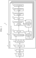
- FIG. 1 is a block diagram illustrating a configuration example of an optical receiver 1 according to Embodiment 1.
- An optical signal received by the optical receiver 1 is obtained by performing frequency division multiplexing on asynchronous optical signals transmitted from a plurality of communicating parties as subcarrier signals.
- FIG. 1 illustrates a case where the optical receiver 1 can receive an optical signal in which four subcarrier signals at maximum are multiplexed.
- the optical receiver 1 includes a coherent detector 2, an ADC 3, and a reception DPS 4.
- the reception DSP 4 includes an FFT unit 41, a division unit 42, and a subcarrier demodulation unit 43 for each subcarrier signal.
- the subcarrier demodulation unit 43 includes a multiplication unit 431, an IFFT unit 432, a number-of-samples adjustment unit 433, an FIFO 434, an adaptive equalization unit 435, a phase compensation unit 436, a demapping unit 437, a clock frequency difference estimation unit 438, and a clock frequency difference compensation unit 439.
- FIG. 2 is a flowchart illustrating an optical reception method according to Embodiment 1, and illustrates an operation of the reception DSP 4 included in the optical receiver 1.
- the coherent detector 2 coherently detects an optical signal received by the optical receiver 1, and converts the optical signal into an electrical signal.
- the ADC 3 is an analog-to-digital converter that converts the electrical signal coherently detected and acquired by the coherent detector 2 into a digital signal.
- the digital signal obtained by conversion by the ADC 3 is output to the FFT unit 41 that is a Fourier transform unit.
- the FFT unit 41 performs Fourier transform on the digital signal converted by the ADC 3 into a signal in a frequency domain (step ST1).
- the division unit 42 divides the signal in the frequency domain converted by the FFT unit 41 into a signal in the frequency domain corresponding to each subcarrier signal (step ST2).
- the signals divided by the division unit 42 are input to the respective individual subcarrier demodulation units 43.
- the multiplication unit 431 multiplies the signal input to the subcarrier demodulation unit 43 with a filter coefficient for compensating for wavelength dispersion and adjusting delay (step ST3).
- the signal multiplied with the filter coefficient by the multiplication unit 431 is output to the IFFT unit 432 that is an inverse Fourier transform unit. Note that the filter coefficient is output from the clock frequency difference compensation unit 439 to the multiplication unit 431.
- the IFFT unit 432 performs inverse Fourier transform on the signal multiplied with the filter coefficient into a signal in a time domain (step ST4).
- the FFT unit 41 and the IFFT unit 432 perform Fourier transform and inverse Fourier transform on a plurality of samples corresponding to signals in a continuous time.
- the FFT unit 41 and the IFFT unit 432 perform transform by overlapping sections in the time domain to prevent deterioration of signals at a seam of the sections in which Fourier transform and inverse Fourier transform are performed.
- the IFFT unit 432 eliminates the above overlap portion in the signal subjected to inverse Fourier transform, adds one extra sample to the end of the signal every inverse Fourier transform, and outputs the signal to the number-of-samples adjustment unit 433.
- the number-of-samples adjustment unit 433 adjusts the number of samples in accordance with a number-of-samples signal from the clock frequency difference estimation unit 438 (step ST5).
- the signal whose number of samples is adjusted by the number-of-samples adjustment unit 433 is output to the FIFO 434.
- the FIFO 434 is a first-in first-out memory, and temporarily stores the signal output by the number-of-samples adjustment unit 433.
- the FIFO 434 outputs the signals, output in the stored order to the adaptive equalization unit 435 in response to a request from the adaptive equalization unit 435 (step ST6). Note that, when the number of stored signals decreases, and the FIFO 434 cannot output signals requested from the adaptive equalization unit 435, the FIFO 434 notifies the adaptive equalization unit 435 that the signals cannot be output.
- the adaptive equalization unit 435 adaptively equalizes the signal output by the FIFO 434 using an FIR filter that is an equalization filter (step ST7). For example, the adaptive equalization unit 435 updates an adaptive equalization filter coefficient in such a way that a distribution of the signals to be output is close to an ideal signal distribution. Note that a least mean square algorithm or the like is used for update.
- the phase compensation unit 436 compensates for phase shift (phase error) of the signal adaptively equalized by the adaptive equalization unit 435 (step ST8).
- the phase compensation unit 436 performs phase compensation using the Vitervi-Viterbi algorithm described in Reference Literature 1.
- the demapping unit 437 receives an input of the signal whose phase shift has been compensated for by the phase compensation unit 436, and demaps the input signal (step ST9).
- the clock frequency difference estimation unit 438 detects a clock phase of the signal whose number of samples has been adjusted by the number-of-samples adjustment unit 433. For example, the clock frequency difference estimation unit 438 detects the clock phase of a received signal on the basis of a change in the strength of the received signal using methods described in Reference Literature 2 and Reference Literature 3.
- the clock frequency difference estimation unit 438 calculates an estimation value of the clock frequency difference, by using a detection value of the clock phase detected from the signal output by the number-of-samples adjustment unit 433 as an estimation value through the low pass filter, and multiplying the estimation value with a negative constant multiple (step ST10).
- the clock frequency difference estimation unit 438 determines a sampling phase for each Fourier transform depending on the estimation value of the clock frequency difference, and outputs a delay selection signal to the clock frequency difference compensation unit 439.
- the delay selection signal is a signal that allows selection of a filter coefficient associated with a delay amount corresponding to the sampling phase determined by the clock frequency difference estimation unit 438 from a coefficient LUT.
- the coefficient LUT is lookup table information in which a plurality of filter coefficients used to compensate for wavelength dispersion and adjust delay, are stored, and is provided for each subcarrier demodulation unit 43.
- the clock frequency difference estimation unit 438 When the sampling phase exceeds 2 ⁇ in a positive direction, the clock frequency difference estimation unit 438 outputs, to the number-of-samples adjustment unit 433, a number-of-samples signal indicating the number of samples that is a number obtained by discarding two samples at the end of the signal from the IFFT unit 432 and decreasing the number of samples by two.
- the clock frequency difference estimation unit 438 outputs to the number-of-samples adjustment unit 433 a number-of-samples signal indicating the number of samples that does not change from the number of samples of the signal from the IFFT unit 432.
- the clock frequency difference estimation unit 438 outputs to the number-of-samples adjustment unit 433 a number-of-samples signal indicating the number of samples obtained by discarding one sample at the end of the signal from the IFFT unit 432 and decreasing the number of samples by one.
- the clock frequency difference compensation unit 439 compensates for wavelength dispersion in an optical transmission path, and stores in the coefficient LUT a plurality of filter coefficients that cause delay (step ST11).
- the coefficient LUT stores the plurality of filter coefficients associated with a plurality of delay amounts.
- the clock frequency difference compensation unit 439 selects a filter coefficient associated with the delay amount selected by the clock frequency difference estimation unit 438 from the coefficient LUT using the delay selection signal, and outputs the filter coefficient to the multiplication unit 431.
- a filter coefficient H (f) is expressed by the following equation (1).
- f represents the frequency
- ⁇ represents the sampling phase
- j represents an imaginary number unit
- D represents wavelength dispersion
- ⁇ represents the wavelength of light
- c represents the light speed
- f s represents the sampling frequency.
- H f exp ⁇ j ⁇ D/2 ⁇ ⁇ 2 / 2 ⁇ c ⁇ 2 ⁇ f 2 exp j ⁇ f/f s ⁇ ⁇
- the filter coefficient H(f) is calculated as a delay amount corresponding to a sampling phase obtained by dividing 0 to 2 ⁇ into, for example, 16 sections, and is stored in the coefficient LUT.
- the clock frequency difference estimation unit 438 approximately selects the filter coefficient depending on the delay amount.
- the optical receiver 1 detects a clock phase of a signal in a time domain whose number of samples has been adjusted, estimates a clock frequency difference from a received signal using a detection value of the clock phase, determines a sampling phase for each FFT depending on an estimation value of the clock frequency difference, selects from the coefficient LUT the filter coefficient associated with a delay amount corresponding to the sampling phase, and multiplies a signal divided by the division unit with the selected filter coefficient.
- the optical receiver 1 compensates for the clock frequency difference by dividing subcarrier signals per frequency band and compensating for wavelength dispersion for a signal in the frequency domain obtained by performing FFT on the received signal, adjusting delay at a low speed on the basis of the estimation value of the clock frequency difference, and adjusting remaining delay at a high speed by adaptive equalization. Consequently, the optical receiver 1 can suppress an increase in power consumption required to clock synchronization with communicating parties.
- Wavelength dispersion of an optical signal in an optical transmission path is inevitable during optical fiber communication.
- conventional optical receivers have required circuits that compensate for wavelength dispersion.
- the optical receiver 1 shares the same filter for compensation for wavelength dispersion and delay adjustment, and consequently does not need an FIR filter for delay adjustment.
- a large circuit resource is necessary to implement a multiplier on a digital signal processing circuit.
- the FIR filter needs the multiplier.
- the optical receiver 1 does not need a multiplier although the number of filter coefficients to be stored in the coefficient LUT increases. Consequently, the optical receiver 1 makes it possible to reduce the circuit scale.
- the clock frequency difference estimation unit detects a clock phase of a received signal in the optical receiver according to Embodiment 1
- an adaptive equalization unit detects a clock phase in an optical receiver according to Embodiment 2.
- FIG. 3 is a block diagram illustrating a configuration of an optical receiver 1A according to Embodiment 2.
- an optical signal received by the optical receiver 1A is obtained by performing frequency division multiplexing on asynchronous optical signals transmitted from a plurality of communicating parties as subcarrier signals.
- FIG. 3 illustrates a case where the optical receiver 1A can receive an optical signal in which four subcarrier signals at maximum are multiplexed.
- the optical receiver 1A includes the coherent detector 2, the ADC 3, and a reception DPS 4A.
- the reception DSP 4A includes the FFT unit 41, the division unit 42, and a subcarrier demodulation unit 43A.
- the subcarrier demodulation unit 43A includes the multiplication unit 431, the IFFT unit 432, the number-of-samples adjustment unit 433, the FIFO 434, an adaptive equalization unit 435A, the phase compensation unit 436, the demapping unit 437, a clock frequency difference estimation unit 438A, and the clock frequency difference compensation unit 439.
- the adaptive equalization unit 435A adaptively equalizes the signal output by the FIFO 434 using the FIR filter similarly to Embodiment 1. Furthermore, the adaptive equalization unit 435A detects a clock phase on the basis of the inclination of phase characteristics in the frequency domain of the FIR filter that is the equalization filter, and outputs the detected clock phase to the clock frequency difference estimation unit 438A.
- the clock frequency difference estimation unit 438A calculates, as an estimation value of a clock frequency difference, a value obtained by multiplying a detection value of the clock phase detected by the adaptive equalization unit 435A with the negative constant multiple through the low pass filter.
- the adaptive equalization unit 435A performs Fourier transform on an adaptive equalization filter coefficient of the FIR filter into a signal in the frequency domain, linearly approximates a change in the frequency of the phase of the signal as the phase characteristics of the signal in the frequency domain, and detects the clock phase of a received signal from a linear inclination that indicates the linearly approximated change.
- the adaptive equalization unit 435A outputs the detected clock phase to the clock frequency difference estimation unit 438A.
- the clock frequency difference estimation unit 438A calculates the estimation value of the clock frequency difference, by using the clock phase detected by the adaptive equalization unit 435A as an estimation value through the low pass filter, and multiplying the estimation value with the negative constant multiple. Furthermore, in a case where the inclination of the clock phase is expressed as ⁇ /f s with respect to the sampling frequency f s , the clock phase is expressed as the sampling phase ⁇ .
- the adaptive equalization unit 435A detects the clock phase on the basis of the inclination of the phase characteristics in the frequency domain of the FIR filter, and outputs the detected clock phase to the clock frequency difference estimation unit 438A.
- the clock frequency difference estimation unit 438A calculates, as an estimation value of a clock frequency difference, a value obtained by multiplying a detection value of the clock phase, which is detected by the adaptive equalization unit 435A, with the negative constant multiple through the low pass filter.
- the optical receiver 1A does not need the FIR filter for delay adjustment. Furthermore, the optical receiver 1A detects the clock phase of the received signal on the basis of the adaptive equalization filter coefficient of the FIR filter of the adaptive equalization unit 435A, and consequently does not need a clock phase detection circuit in the clock frequency difference estimation unit 438A.
- the filter length of the FIR filter in the adaptive equalization unit 435A is approximately 20, and a circuit for performing Fourier transform and linear approximation for detecting the clock phase is sufficiently small, so that it is possible to reduce the circuit scale necessary for detection of the clock phase.
- the functions of the reception DSPs 4 and 4A included in the optical receivers 1 and 1A are implemented by a processing circuit. That is, the optical receivers 1 and 1A include the processing circuit for executing processing in steps ST1 to ST11 illustrated in FIG. 2 .
- the processing circuit may be dedicated hardware, yet may be a Central Processing Unit (CPU) that executes programs stored in a memory.
- CPU Central Processing Unit
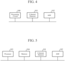
- FIG. 4 is a block diagram illustrating the hardware configuration that implements the functions of the optical receivers 1 and 1A.
- FIG. 5 is a block diagram illustrating a hardware configuration that executes software that implements the functions of the optical receivers 1 and 1A.
- a coherent detector 101 is the coherent detector 2 illustrated in FIGS. 1 and 3 .
- An ADC 102 is the ADC 3 illustrated in FIGS. 1 and 3 .
- the processing circuit 100 corresponds to, for example, a single circuit, a composite circuit, a programmed processor, a parallel-programmed processor, an Application Specific Integrated Circuit (ASIC), a Field-Programmable Gate Array (FPGA), or a combination thereof.
- the functions of the FFT unit, the division unit, and the subcarrier demodulation unit included in the optical receivers 1 and 1A may be implemented as different processing circuits, and these functions may be implemented collectively by one processing circuit.
- the functions of the FFT unit, the division unit, and the subcarrier demodulation unit included in the optical receivers 1 and 1A are implemented by software, firmware, or a combination of software and firmware. Note that the software or the firmware is described as programs, and stored in a memory 104.
- the processor 103 implements the functions of the FFT unit, the division unit, and the subcarrier demodulation unit by reading and executing the programs stored in the memory 104.
- the FFT unit, the division unit, and the subcarrier demodulation unit included in the optical receivers 1 and 1A include the memory 104 for storing the programs for eventually executing the processing in steps ST1 to ST11 illustrated in FIG. 2 when the processor 103 executes the programs.
- the memory 104 may be a computer-readable storage medium having recorded thereon the programs for causing the computer to function as the FFT unit, the division unit, and the subcarrier demodulation unit.
- the memory 104 corresponds to, for example, a non-volatile or volatile semiconductor memory such as a Random Access Memory (RAM), a Read Only Memory (ROM), a flash memory, an Erasable Programmable Read Only Memory (EPROM), or an Electrically-EPROM (EEPROM), a magnetic disk, a flexible disk, an optical disk, a compact disk, a mini disk, a DVD, or the like.
- RAM Random Access Memory
- ROM Read Only Memory
- EPROM Erasable Programmable Read Only Memory
- EEPROM Electrically-EPROM
- Part of the functions of the FFT unit, the division unit, and the subcarrier demodulation unit included in the optical receivers 1 and 1A may be implemented as dedicated hardware, and part of the functions may be implemented by software or firmware.
- the functions of the FFT unit and the division unit may be implemented by the processing circuit 102 that is the dedicated hardware, and the function of the subcarrier demodulation unit may be implemented by the processor 103 by reading and executing the programs stored in the memory 104.
- the processing circuit can implement the above functions by hardware, software, firmware, or a combination thereof.
- the optical receiver according to the present disclosure can be used for optical communication of a digital coherent system, for example.
- 1, 1A optical receiver. 2, 101: coherent detector. 3, 102: ADC. 4, 4A: reception DSP. 41: FFT unit. 42: division unit. 43, 43A: subcarrier demodulation unit. 100: processing circuit. 101: coherent detector. 103: processor. 104: memory. 431: multiplication unit. 432: IFFT unit. 433: number-of-samples adjustment unit. 435, 435A: adaptive equalization unit. 436: phase compensation unit. 437: demapping unit. 438, 438A: clock frequency difference estimation unit. 439: clock frequency difference compensation unit
Landscapes
- Engineering & Computer Science (AREA)
- Computer Networks & Wireless Communication (AREA)
- Signal Processing (AREA)
- Physics & Mathematics (AREA)
- Electromagnetism (AREA)
- Optics & Photonics (AREA)
- Optical Communication System (AREA)
Abstract
Description
- The present disclosure relates to an optical receiver and an optical reception method.
- In recent years, the bands of digital analog converters (hereinafter, simply referred to as DACs) and analog digital converters (hereinafter, simply referred to as ADCs) mounted on large-scale integrated circuits (hereinafter, referred to as a DSP-LSIs) that perform digital signal processing for optical communication of a digital coherent system continue broadening. The bands of optical parts that constitute optical transceivers also continue broadening in addition to DACs and ADCs mounted on DSP-LSIs, and the optical transceivers as a whole have larger capacity and broader bands.
- To utilize a large-volume throughput and a wider band of an optical transceiver, a DSP-LSI multiplexes subcarriers. Consequently, one optical transceiver supports communication with a plurality of communicating parties and simultaneously supports signal accommodation of a plurality of services, so that the optical transceiver can contribute to efficiently constructing metro and access networks.
- In this regard, although it is necessary to perform clock synchronization for a signal transmitted from each of the communicating parties to support communication with the plurality of communicating parties, a configuration of the optical transceiver is complicated in a case where a plurality of clock sources are mounted on the optical transceiver for communication with the plurality of communicating parties. By contrast with this, for example, a conventional technique described in Non-Patent Literature 1 achieves clock synchronization by performing resampling in synchronization with clocks as digital signal processing in a DSP-LSI.
- An optical receiver described in Non-Patent Literature 1 performs division and dispersion compensation on subcarriers in a frequency domain, and then dynamically changes a Finite Impulse Response filter (hereinafter, referred to as an FIR filter.) coefficient in a time domain to adjust delay. Thus, a clock frequency difference between a received signal and the optical receiver is compensated for.
- Non-Patent Literature 1: D. Schmidt and B. Lankl, "Structure of a Digital Feedback Clock Recovery for Parallelized Receivers," in Advanced Photonics, OSA Technical Digest (CD) (Optical Society of America, 2011), paper SPTuC2.
- However, the conventional technique described in Non-Patent Literature 1 needs to adjust delay using the FIR filter, and therefore has a problem that a circuit scale of the DSP-LSI increases and power consumption increases.
- The present disclosure solves the above problem, and an object of the present disclosure is to provide an optical receiver and an optical reception method that can suppress an increase in power consumption required to clock synchronization with communicating parties.
- An optical receiver according to the present disclosure is an optical receiver to receive an optical signal in which a plurality of subcarrier signals have been subjected to frequency division multiplexing, and includes: a coherent detector to coherently detect the optical signal, and convert the optical signal into an electrical signal; an ADC to convert a received signal converted into the electrical signal by the coherent detector into a digital signal; a Fourier transform unit to perform Fourier transform on the received signal converted into the digital signal by the ADC into a signal in a frequency domain; a division unit to divide the signal in the frequency domain converted by the Fourier transform unit into a signal per frequency band of each of the subcarrier signals; and a plurality of subcarrier demodulation units to each demodulate a corresponding one of the subcarrier signals, by multiplying the signal divided by the division unit with a filter coefficient for compensating for wavelength dispersion and adjusting delay of the optical signal in an optical transmission path, converting the signal multiplied with the filter coefficient into a signal in a time domain, adaptively equalizing the signal in the time domain whose number of samples has been adjusted, compensating for phase shift of the equalized signal, and demapping the signal whose phase shift has been compensated for, the plurality of subcarrier demodulation units being each provided per frequency band of each of the subcarrier signals, and the subcarrier demodulation units each include a lookup table in which a plurality of the filter coefficients are stored depending on delay amounts, detect a clock phase of the signal in the time domain whose number of samples has been adjusted, estimate a clock frequency difference from the received signal using a detection value of the clock phase, determine a sampling phase for each Fourier transform depending on an estimation value of the clock frequency difference, select from the lookup table the filter coefficient associated with the delay amount corresponding to the determined sampling phase, and multiply the signal divided by the division unit with the selected filter coefficient.
- According to the present disclosure, a clock phase of a signal in a time domain whose number of samples has been adjusted is detected, a clock frequency difference from a received signal is estimated using a detection value of the clock phase, a sampling phase for each Fourier transform is determined depending on an estimation value of the clock frequency difference, a filter coefficient associated with a delay amount corresponding to the sampling phase is selected from a lookup table in which a plurality of filter coefficients for compensating wavelength dispersion and adjusting delay of an optical signal in an optical transmission path are stored, and a signal divided by a division unit is multiplied with the selected filter coefficient. Consequently, the optical receiver according to the present disclosure can suppress an increase in power consumption required to clock synchronization with communicating parties.
-
-
FIG. 1 is a block diagram illustrating a configuration example of an optical receiver according to Embodiment 1. -
FIG. 2 is a flowchart illustrating an optical reception method according to Embodiment 1. -
FIG. 3 is a block diagram illustrating a configuration example of an optical receiver according to Embodiment 2. -
FIG. 4 is a block diagram illustrating a hardware configuration that implements the functions of the optical receivers according to Embodiment 1 and Embodiment 2. -
FIG. 5 is a block diagram illustrating a hardware configuration that executes software that implements the functions of the optical receivers according to Embodiment 1 and Embodiment 2. -
FIG. 1 is a block diagram illustrating a configuration example of an optical receiver 1 according to Embodiment 1. An optical signal received by the optical receiver 1 is obtained by performing frequency division multiplexing on asynchronous optical signals transmitted from a plurality of communicating parties as subcarrier signals.FIG. 1 illustrates a case where the optical receiver 1 can receive an optical signal in which four subcarrier signals at maximum are multiplexed. - As illustrated in
FIG. 1 , the optical receiver 1 includes a coherent detector 2, an ADC 3, and a reception DPS 4. The reception DSP 4 includes anFFT unit 41, adivision unit 42, and asubcarrier demodulation unit 43 for each subcarrier signal. Thesubcarrier demodulation unit 43 includes amultiplication unit 431, anIFFT unit 432, a number-of-samples adjustment unit 433, anFIFO 434, anadaptive equalization unit 435, aphase compensation unit 436, ademapping unit 437, a clock frequency difference estimation unit 438, and a clock frequencydifference compensation unit 439. -
FIG. 2 is a flowchart illustrating an optical reception method according to Embodiment 1, and illustrates an operation of the reception DSP 4 included in the optical receiver 1. First, the coherent detector 2 coherently detects an optical signal received by the optical receiver 1, and converts the optical signal into an electrical signal. The ADC 3 is an analog-to-digital converter that converts the electrical signal coherently detected and acquired by the coherent detector 2 into a digital signal. The digital signal obtained by conversion by the ADC 3 is output to theFFT unit 41 that is a Fourier transform unit. - In the reception DSP 4, the
FFT unit 41 performs Fourier transform on the digital signal converted by the ADC 3 into a signal in a frequency domain (step ST1). Thedivision unit 42 divides the signal in the frequency domain converted by theFFT unit 41 into a signal in the frequency domain corresponding to each subcarrier signal (step ST2). The signals divided by thedivision unit 42 are input to the respective individualsubcarrier demodulation units 43. - The
multiplication unit 431 multiplies the signal input to thesubcarrier demodulation unit 43 with a filter coefficient for compensating for wavelength dispersion and adjusting delay (step ST3). The signal multiplied with the filter coefficient by themultiplication unit 431 is output to theIFFT unit 432 that is an inverse Fourier transform unit. Note that the filter coefficient is output from the clock frequencydifference compensation unit 439 to themultiplication unit 431. - The
IFFT unit 432 performs inverse Fourier transform on the signal multiplied with the filter coefficient into a signal in a time domain (step ST4). TheFFT unit 41 and theIFFT unit 432 perform Fourier transform and inverse Fourier transform on a plurality of samples corresponding to signals in a continuous time. In this regard, theFFT unit 41 and theIFFT unit 432 perform transform by overlapping sections in the time domain to prevent deterioration of signals at a seam of the sections in which Fourier transform and inverse Fourier transform are performed. TheIFFT unit 432 eliminates the above overlap portion in the signal subjected to inverse Fourier transform, adds one extra sample to the end of the signal every inverse Fourier transform, and outputs the signal to the number-of-samples adjustment unit 433. - The number-of-
samples adjustment unit 433 adjusts the number of samples in accordance with a number-of-samples signal from the clock frequency difference estimation unit 438 (step ST5). The signal whose number of samples is adjusted by the number-of-samples adjustment unit 433 is output to theFIFO 434. The FIFO 434 is a first-in first-out memory, and temporarily stores the signal output by the number-of-samples adjustment unit 433. - The FIFO 434 outputs the signals, output in the stored order to the
adaptive equalization unit 435 in response to a request from the adaptive equalization unit 435 (step ST6). Note that, when the number of stored signals decreases, and the FIFO 434 cannot output signals requested from theadaptive equalization unit 435, the FIFO 434 notifies theadaptive equalization unit 435 that the signals cannot be output. - The
adaptive equalization unit 435 adaptively equalizes the signal output by the FIFO 434 using an FIR filter that is an equalization filter (step ST7). For example, theadaptive equalization unit 435 updates an adaptive equalization filter coefficient in such a way that a distribution of the signals to be output is close to an ideal signal distribution. Note that a least mean square algorithm or the like is used for update. - The
phase compensation unit 436 compensates for phase shift (phase error) of the signal adaptively equalized by the adaptive equalization unit 435 (step ST8). For example, thephase compensation unit 436 performs phase compensation using the Vitervi-Viterbi algorithm described in Reference Literature 1. The demappingunit 437 receives an input of the signal whose phase shift has been compensated for by thephase compensation unit 436, and demaps the input signal (step ST9). - (Reference Literature 1) A. J. Viterbi and A. M. Viterbi, "Nonlinear estimation of PSK-modulated carrier phase with application to burst digital transmission," Trans. Inf. Theory, Vol. 29, No. 4, pp. 543-551, Jul. 1983.
- The clock frequency difference estimation unit 438 detects a clock phase of the signal whose number of samples has been adjusted by the number-of-
samples adjustment unit 433. For example, the clock frequency difference estimation unit 438 detects the clock phase of a received signal on the basis of a change in the strength of the received signal using methods described in Reference Literature 2 and Reference Literature 3. - (Reference Literature 2) F. Gardner, "A BPSK/QPSK Timing-Error Detector for Sampled Receivers," in IEEE Transactions on Communications, vol. 34, no. 5, pp. 423-429, May 1986.
- (Reference Literature 3) Meng Yan et al., "Digital clock recovery algorithm for Nyquist signal," 2013 Optical Fiber Communication Conference and Exposition and the National Fiber Optic Engineers Conference (OFC/NFOEC), paper OTu2I.7, 2013.
- Next, the clock frequency difference estimation unit 438 calculates an estimation value of the clock frequency difference, by using a detection value of the clock phase detected from the signal output by the number-of-
samples adjustment unit 433 as an estimation value through the low pass filter, and multiplying the estimation value with a negative constant multiple (step ST10). The clock frequency difference estimation unit 438 determines a sampling phase for each Fourier transform depending on the estimation value of the clock frequency difference, and outputs a delay selection signal to the clock frequencydifference compensation unit 439. The delay selection signal is a signal that allows selection of a filter coefficient associated with a delay amount corresponding to the sampling phase determined by the clock frequency difference estimation unit 438 from a coefficient LUT. - Note that the coefficient LUT is lookup table information in which a plurality of filter coefficients used to compensate for wavelength dispersion and adjust delay, are stored, and is provided for each
subcarrier demodulation unit 43. - When the sampling phase exceeds 2π in a positive direction, the clock frequency difference estimation unit 438 outputs, to the number-of-
samples adjustment unit 433, a number-of-samples signal indicating the number of samples that is a number obtained by discarding two samples at the end of the signal from theIFFT unit 432 and decreasing the number of samples by two. - Furthermore, when the sampling phase exceeds 0 in a negative direction, the clock frequency difference estimation unit 438 outputs to the number-of-samples adjustment unit 433 a number-of-samples signal indicating the number of samples that does not change from the number of samples of the signal from the
IFFT unit 432. - In another case, the clock frequency difference estimation unit 438 outputs to the number-of-samples adjustment unit 433 a number-of-samples signal indicating the number of samples obtained by discarding one sample at the end of the signal from the
IFFT unit 432 and decreasing the number of samples by one. - The clock frequency
difference compensation unit 439 compensates for wavelength dispersion in an optical transmission path, and stores in the coefficient LUT a plurality of filter coefficients that cause delay (step ST11). The coefficient LUT stores the plurality of filter coefficients associated with a plurality of delay amounts. The clock frequencydifference compensation unit 439 selects a filter coefficient associated with the delay amount selected by the clock frequency difference estimation unit 438 from the coefficient LUT using the delay selection signal, and outputs the filter coefficient to themultiplication unit 431. A filter coefficient H (f) is expressed by the following equation (1). In the following equation (1), f represents the frequency, ψ represents the sampling phase, j represents an imaginary number unit, D represents wavelength dispersion, λ represents the wavelength of light, c represents the light speed, and fs represents the sampling frequency.
- The filter coefficient H(f) is calculated as a delay amount corresponding to a sampling phase obtained by dividing 0 to 2π into, for example, 16 sections, and is stored in the coefficient LUT. The clock frequency difference estimation unit 438 approximately selects the filter coefficient depending on the delay amount.
- As described above, the optical receiver 1 according to Embodiment 1 detects a clock phase of a signal in a time domain whose number of samples has been adjusted, estimates a clock frequency difference from a received signal using a detection value of the clock phase, determines a sampling phase for each FFT depending on an estimation value of the clock frequency difference, selects from the coefficient LUT the filter coefficient associated with a delay amount corresponding to the sampling phase, and multiplies a signal divided by the division unit with the selected filter coefficient.
- The optical receiver 1 compensates for the clock frequency difference by dividing subcarrier signals per frequency band and compensating for wavelength dispersion for a signal in the frequency domain obtained by performing FFT on the received signal, adjusting delay at a low speed on the basis of the estimation value of the clock frequency difference, and adjusting remaining delay at a high speed by adaptive equalization. Consequently, the optical receiver 1 can suppress an increase in power consumption required to clock synchronization with communicating parties.
- Wavelength dispersion of an optical signal in an optical transmission path is inevitable during optical fiber communication. Hence, conventional optical receivers have required circuits that compensate for wavelength dispersion. By contrast with this, as described above, the optical receiver 1 shares the same filter for compensation for wavelength dispersion and delay adjustment, and consequently does not need an FIR filter for delay adjustment. Furthermore, a large circuit resource is necessary to implement a multiplier on a digital signal processing circuit. Furthermore, the FIR filter needs the multiplier. By contrast with this, the optical receiver 1 does not need a multiplier although the number of filter coefficients to be stored in the coefficient LUT increases. Consequently, the optical receiver 1 makes it possible to reduce the circuit scale.
- Although the clock frequency difference estimation unit detects a clock phase of a received signal in the optical receiver according to Embodiment 1, an adaptive equalization unit detects a clock phase in an optical receiver according to Embodiment 2.
-
FIG. 3 is a block diagram illustrating a configuration of anoptical receiver 1A according to Embodiment 2. InFIG. 3 , an optical signal received by theoptical receiver 1A is obtained by performing frequency division multiplexing on asynchronous optical signals transmitted from a plurality of communicating parties as subcarrier signals.FIG. 3 illustrates a case where theoptical receiver 1A can receive an optical signal in which four subcarrier signals at maximum are multiplexed. - As illustrated in
FIG. 3 , theoptical receiver 1A includes the coherent detector 2, the ADC 3, and areception DPS 4A. Thereception DSP 4A includes theFFT unit 41, thedivision unit 42, and asubcarrier demodulation unit 43A. Thesubcarrier demodulation unit 43A includes themultiplication unit 431, theIFFT unit 432, the number-of-samples adjustment unit 433, theFIFO 434, anadaptive equalization unit 435A, thephase compensation unit 436, thedemapping unit 437, a clock frequencydifference estimation unit 438A, and the clock frequencydifference compensation unit 439. - The
adaptive equalization unit 435A adaptively equalizes the signal output by theFIFO 434 using the FIR filter similarly to Embodiment 1. Furthermore, theadaptive equalization unit 435A detects a clock phase on the basis of the inclination of phase characteristics in the frequency domain of the FIR filter that is the equalization filter, and outputs the detected clock phase to the clock frequencydifference estimation unit 438A. The clock frequencydifference estimation unit 438A calculates, as an estimation value of a clock frequency difference, a value obtained by multiplying a detection value of the clock phase detected by theadaptive equalization unit 435A with the negative constant multiple through the low pass filter. - For example, the
adaptive equalization unit 435A performs Fourier transform on an adaptive equalization filter coefficient of the FIR filter into a signal in the frequency domain, linearly approximates a change in the frequency of the phase of the signal as the phase characteristics of the signal in the frequency domain, and detects the clock phase of a received signal from a linear inclination that indicates the linearly approximated change. Theadaptive equalization unit 435A outputs the detected clock phase to the clock frequencydifference estimation unit 438A. - The clock frequency
difference estimation unit 438A calculates the estimation value of the clock frequency difference, by using the clock phase detected by theadaptive equalization unit 435A as an estimation value through the low pass filter, and multiplying the estimation value with the negative constant multiple. Furthermore, in a case where the inclination of the clock phase is expressed as ψ/fs with respect to the sampling frequency fs, the clock phase is expressed as the sampling phase ψ. - As described above, in the
optical receiver 1A according to Embodiment 2, theadaptive equalization unit 435A detects the clock phase on the basis of the inclination of the phase characteristics in the frequency domain of the FIR filter, and outputs the detected clock phase to the clock frequencydifference estimation unit 438A. The clock frequencydifference estimation unit 438A calculates, as an estimation value of a clock frequency difference, a value obtained by multiplying a detection value of the clock phase, which is detected by theadaptive equalization unit 435A, with the negative constant multiple through the low pass filter. - Similarly to Embodiment 1, the
optical receiver 1A does not need the FIR filter for delay adjustment. Furthermore, theoptical receiver 1A detects the clock phase of the received signal on the basis of the adaptive equalization filter coefficient of the FIR filter of theadaptive equalization unit 435A, and consequently does not need a clock phase detection circuit in the clock frequencydifference estimation unit 438A. - Note that the filter length of the FIR filter in the
adaptive equalization unit 435A is approximately 20, and a circuit for performing Fourier transform and linear approximation for detecting the clock phase is sufficiently small, so that it is possible to reduce the circuit scale necessary for detection of the clock phase. - Next, a hardware configuration that implements the functions of the
optical receivers 1 and 1A according to Embodiment 1 and Embodiment 2 will be described. - The functions of the
reception DSPs 4 and 4A included in theoptical receivers 1 and 1A are implemented by a processing circuit. That is, theoptical receivers 1 and 1A include the processing circuit for executing processing in steps ST1 to ST11 illustrated inFIG. 2 . The processing circuit may be dedicated hardware, yet may be a Central Processing Unit (CPU) that executes programs stored in a memory. -
FIG. 4 is a block diagram illustrating the hardware configuration that implements the functions of theoptical receivers 1 and 1A.FIG. 5 is a block diagram illustrating a hardware configuration that executes software that implements the functions of theoptical receivers 1 and 1A. InFIGS. 4 and 5 , acoherent detector 101 is the coherent detector 2 illustrated inFIGS. 1 and3 . AnADC 102 is the ADC 3 illustrated inFIGS. 1 and3 . - In a case where the above processing circuit is a
processing circuit 100 of the dedicated hardware illustrated inFIG. 4 , theprocessing circuit 100 corresponds to, for example, a single circuit, a composite circuit, a programmed processor, a parallel-programmed processor, an Application Specific Integrated Circuit (ASIC), a Field-Programmable Gate Array (FPGA), or a combination thereof. The functions of the FFT unit, the division unit, and the subcarrier demodulation unit included in theoptical receivers 1 and 1A may be implemented as different processing circuits, and these functions may be implemented collectively by one processing circuit. - In a case where the above processing circuit is a
processor 103 illustrated inFIG. 5 , the functions of the FFT unit, the division unit, and the subcarrier demodulation unit included in theoptical receivers 1 and 1A are implemented by software, firmware, or a combination of software and firmware. Note that the software or the firmware is described as programs, and stored in amemory 104. - The
processor 103 implements the functions of the FFT unit, the division unit, and the subcarrier demodulation unit by reading and executing the programs stored in thememory 104. For example, the FFT unit, the division unit, and the subcarrier demodulation unit included in theoptical receivers 1 and 1A include thememory 104 for storing the programs for eventually executing the processing in steps ST1 to ST11 illustrated inFIG. 2 when theprocessor 103 executes the programs. - These programs cause a computer to execute a processing procedure or method performed by the FFT unit, the division unit, and the subcarrier demodulation unit included in the
optical receivers 1 and 1A. Thememory 104 may be a computer-readable storage medium having recorded thereon the programs for causing the computer to function as the FFT unit, the division unit, and the subcarrier demodulation unit. - The
memory 104 corresponds to, for example, a non-volatile or volatile semiconductor memory such as a Random Access Memory (RAM), a Read Only Memory (ROM), a flash memory, an Erasable Programmable Read Only Memory (EPROM), or an Electrically-EPROM (EEPROM), a magnetic disk, a flexible disk, an optical disk, a compact disk, a mini disk, a DVD, or the like. - Part of the functions of the FFT unit, the division unit, and the subcarrier demodulation unit included in the
optical receivers 1 and 1A may be implemented as dedicated hardware, and part of the functions may be implemented by software or firmware. For example, the functions of the FFT unit and the division unit may be implemented by theprocessing circuit 102 that is the dedicated hardware, and the function of the subcarrier demodulation unit may be implemented by theprocessor 103 by reading and executing the programs stored in thememory 104. Thus, the processing circuit can implement the above functions by hardware, software, firmware, or a combination thereof. - Note that the embodiments can be combined, any components in the embodiments can be modified, or any components in the embodiments can be omitted.
- The optical receiver according to the present disclosure can be used for optical communication of a digital coherent system, for example.
- 1, 1A: optical receiver. 2, 101: coherent detector. 3, 102: ADC. 4, 4A: reception DSP. 41: FFT unit. 42: division unit. 43, 43A: subcarrier demodulation unit. 100: processing circuit. 101: coherent detector. 103: processor. 104: memory. 431: multiplication unit. 432: IFFT unit. 433: number-of-samples adjustment unit. 435, 435A: adaptive equalization unit. 436: phase compensation unit. 437: demapping unit. 438, 438A: clock frequency difference estimation unit. 439: clock frequency difference compensation unit
Claims (6)
- An optical receiver to receive an optical signal in which a plurality of subcarrier signals have been subjected to frequency division multiplexing, the optical receiver comprising:a coherent detector to coherently detect the optical signal, and convert the optical signal into an electrical signal;an analog-digital converter to convert a received signal converted into the electrical signal by the coherent detector into a digital signal;a Fourier transform unit to perform Fourier transform on the received signal converted into the digital signal by the analog-to-digital converter into a signal in a frequency domain;a division unit to divide the signal in the frequency domain converted by the Fourier transform unit into a signal per frequency band of each of the subcarrier signals; anda plurality of subcarrier demodulation units to each demodulate a corresponding one of the subcarrier signals, by multiplying the signal divided by the division unit with a filter coefficient for compensating for wavelength dispersion and adjusting delay of the optical signal in an optical transmission path, converting the signal multiplied with the filter coefficient into a signal in a time domain, adaptively equalizing the signal in the time domain whose number of samples has been adjusted, compensating for phase shift of the equalized signal, and demapping the signal whose phase shift has been compensated for, the plurality of subcarrier demodulation units being each provided per frequency band of each of the subcarrier signals,wherein the subcarrier demodulation units eachinclude a lookup table in which a plurality of the filter coefficients are stored depending on delay amounts,detect a clock phase of the signal in the time domain whose number of samples has been adjusted,estimate a clock frequency difference from the received signal using a detection value of the clock phase, anddetermine a sampling phase for each Fourier transform depending on an estimation value of the clock frequency difference, select from the lookup table the filter coefficient associated with the delay amount corresponding to the determined sampling phase, and multiply the signal divided by the division unit with the selected filter coefficient.
- The optical receiver according to claim 1, wherein the subcarrier demodulation units each include:a multiplication unit to multiply the signal divided by the division unit with the filter coefficient,an inverse Fourier transform unit to perform inverse Fourier transform on the signal multiplied with the filter coefficient into the signal in the time domain, add one extra sample to an end of the signal every inverse Fourier transform, and output the signal,a number-of-samples adjustment unit to adjust the number of samples of the signal in the time domain on a basis of a number-of-samples signal,a first-in first-out memory to store the signal whose number of samples has been adjusted,an adaptive equalization unit to adaptively equalize the signal output from the first-in first-out memory in such a way that the signal is close to an ideal signal point distribution,a phase compensation unit to compensate for the phase shift of the equalized signal,a demapping unit to demap the signal whose phase shift has been compensated for,a clock frequency difference estimation unit to estimate the clock frequency difference from the received signal, determine the sampling phase corresponding to the clock frequency difference every Fourier transform, and select the filter coefficient associated with the delay amount corresponding to the sampling phase, anda clock frequency difference compensation unit to read from the lookup table the filter coefficient selected by the clock frequency difference estimation unit, and output the filter coefficient to the multiplication unit.
- The optical receiver according to claim 2, wherein the clock frequency difference estimation unit detects a clock phase of a signal output from the number-of-samples adjustment unit, and calculates, as an estimation value of the clock frequency difference, a value obtained by multiplying a detection value of the clock phase with a negative constant multiple through a low pass filter.
- The optical receiver according to claim 3, whereinthe number-of-samples adjustment unit adjusts the number of samples of the signal in the time domain converted by the inverse Fourier transform unit in accordance with the number-of-samples signal output from the clock frequency difference estimation unit, andthe clock frequency difference estimation unitoutputs to the number-of-samples adjustment unit a number-of-samples signal for instructing to discard two samples at the end of the signal in the time domain converted by the inverse Fourier transform unit and decrease the number of samples by two when the determined sampling phase exceeds 2π in a positive direction,outputs to the number-of-samples adjustment unit a number-of-samples signal for instructing not to change the number of samples of the signal in the time domain converted by the inverse Fourier transform unit when the determined sampling phase exceeds 0 in a negative direction, andoutputs to the number-of-samples adjustment unit a number-of-samples signal for instructing to discard one sample at the end of the signal in the time domain converted by the inverse Fourier transform unit and decrease the number of samples by one when the determined sampling phase does not exceed 2π in the positive direction, and does not exceed 0 in the negative direction.
- The optical receiver according to claim 3 or 4, whereinthe adaptive equalization unit detects a clock phase on a basis of an inclination of phase characteristics in the frequency domain of an equalization filter, and outputs the detected clock phase to the clock frequency difference estimation unit, andthe clock frequency difference estimation unit calculates, as the estimation value of the clock frequency difference, a value obtained by multiplying the detection value of the clock phase detected by the adaptive equalization unit with the negative constant multiple through the low pass filter.
- An optical reception method of an optical receiver that receives an optical signal in which a plurality of subcarrier signals have been subjected to frequency division multiplexing, and comprises:a coherent detector to coherently detect the optical signal, and convert the optical signal into an electrical signal;an analog-digital converter to convert a received signal converted into the electrical signal by the coherent detector into a digital signal;a Fourier transform unit to perform Fourier transform on the received signal converted into the digital signal by the analog-to-digital converter into a signal in a frequency domain;a division unit to divide the signal in the frequency domain converted by the Fourier transform unit into a signal per frequency band of each of the subcarrier signals; anda plurality of subcarrier demodulation units each provided per frequency band of each of the subcarrier signals, and each including a multiplication unit, an inverse Fourier transform unit, a number-of-samples adjustment unit, a first-in first-out memory, an adaptive equalization unit, a phase compensation unit, a demapping unit, a clock frequency difference estimation unit, and a clock frequency difference compensation unit,the optical reception method comprising:a step of, by the multiplication unit, multiplying the signal divided by the division unit with a filter coefficient for compensating for wavelength dispersion and adjusting delay of the optical signal in an optical transmission path;a step of, by the inverse Fourier transform unit, performing inverse Fourier transform on the signal multiplied with the filter coefficient into a signal in a time domain, adding one extra sample to an end of the signal every inverse Fourier transform, and outputting the signal;a step of, by the number-of-samples adjustment unit, adjusting a number of samples of the signal in the time domain on a basis of a number-of-samples signal;a step of, by the first-in first-out memory, storing the signal whose number of samples has been adjusted;a step of, by the adaptive equalization unit, adaptively equalizing the signal output from the first-in first-out memory in such a way that the signal is close to an ideal signal point distribution;a step of, by the phase compensation unit, compensating for phase shift of the equalized signal;a step of, by the demapping unit, demapping the signal whose phase shift has been compensated for;a step of, by the clock frequency difference estimation unit, estimating a clock frequency difference from the received signal, determining a sampling phase corresponding to the clock frequency difference every Fourier transform, and selecting the filter coefficient associated with the delay amount corresponding to the sampling phase; anda step of, by the clock frequency difference compensation unit, reading the filter coefficient selected by the clock frequency difference estimation unit from a lookup table in which a plurality of the filter coefficients are stored depending on delay amounts, and outputting the filter coefficient to the multiplication unit.
Applications Claiming Priority (1)
| Application Number | Priority Date | Filing Date | Title |
|---|---|---|---|
| PCT/JP2022/005774 WO2023157044A1 (en) | 2022-02-15 | 2022-02-15 | Optical receiver and optical reception method |
Publications (3)
| Publication Number | Publication Date |
|---|---|
| EP4432584A1 true EP4432584A1 (en) | 2024-09-18 |
| EP4432584A4 EP4432584A4 (en) | 2025-01-15 |
| EP4432584B1 EP4432584B1 (en) | 2025-12-24 |
Family
ID=87577700
Family Applications (1)
| Application Number | Title | Priority Date | Filing Date |
|---|---|---|---|
| EP22926949.3A Active EP4432584B1 (en) | 2022-02-15 | 2022-02-15 | Optical receiver and optical reception method |
Country Status (5)
| Country | Link |
|---|---|
| US (1) | US20240356655A1 (en) |
| EP (1) | EP4432584B1 (en) |
| JP (1) | JP7442757B2 (en) |
| CN (1) | CN118661391A (en) |
| WO (1) | WO2023157044A1 (en) |
Families Citing this family (1)
| Publication number | Priority date | Publication date | Assignee | Title |
|---|---|---|---|---|
| WO2021181568A1 (en) * | 2020-03-11 | 2021-09-16 | 日本電信電話株式会社 | Optical reception device and optical reception method |
Family Cites Families (7)
| Publication number | Priority date | Publication date | Assignee | Title |
|---|---|---|---|---|
| JP5444877B2 (en) * | 2009-06-24 | 2014-03-19 | 富士通株式会社 | Digital coherent receiver |
| JP5407595B2 (en) * | 2009-06-30 | 2014-02-05 | 富士通株式会社 | Signal processing circuit, optical receiver, detector, and waveform distortion compensation method |
| CN102308546B (en) * | 2011-07-26 | 2013-12-04 | 华为技术有限公司 | Receiving method and device of multiple carrier optical signal |
| JP6405833B2 (en) * | 2014-09-25 | 2018-10-17 | 富士通株式会社 | Signal processing apparatus and signal processing method |
| US11251878B2 (en) * | 2018-02-07 | 2022-02-15 | Infinera Corporation | Independently routable digital subcarriers for optical communication networks |
| US11418312B2 (en) * | 2019-04-19 | 2022-08-16 | Infinera Corporation | Synchronization for subcarrier communication |
| WO2021181568A1 (en) * | 2020-03-11 | 2021-09-16 | 日本電信電話株式会社 | Optical reception device and optical reception method |
-
2022
- 2022-02-15 JP JP2023576321A patent/JP7442757B2/en active Active
- 2022-02-15 WO PCT/JP2022/005774 patent/WO2023157044A1/en not_active Ceased
- 2022-02-15 EP EP22926949.3A patent/EP4432584B1/en active Active
- 2022-02-15 CN CN202280091136.0A patent/CN118661391A/en active Pending
-
2024
- 2024-06-28 US US18/759,317 patent/US20240356655A1/en active Pending
Also Published As
| Publication number | Publication date |
|---|---|
| EP4432584A4 (en) | 2025-01-15 |
| EP4432584B1 (en) | 2025-12-24 |
| JP7442757B2 (en) | 2024-03-04 |
| CN118661391A (en) | 2024-09-17 |
| WO2023157044A1 (en) | 2023-08-24 |
| JPWO2023157044A1 (en) | 2023-08-24 |
| US20240356655A1 (en) | 2024-10-24 |
Similar Documents
| Publication | Publication Date | Title |
|---|---|---|
| US9628180B2 (en) | Configurable frequency domain equalizer for dispersion compensation of multiple sub-carriers | |
| JP6405833B2 (en) | Signal processing apparatus and signal processing method | |
| JP6733755B2 (en) | Frequency deviation compensation method and frequency deviation compensation method | |
| US8744278B2 (en) | Method for electric power supply of optical receiver, digital signal processing circuit, and optical receiver | |
| US9602219B2 (en) | Efficient processing of high data rate signals with a configurable frequency domain equalizer | |
| JP5158268B2 (en) | Optical receiver and optical reception control method | |
| JP5943001B2 (en) | Equalized signal processing apparatus, optical receiver using the same, and equalized signal processing method | |
| US8918444B2 (en) | Method and device for filterling an input signal | |
| EP2638378B1 (en) | Method and device for estimating a chromatic dispersion of a received optical signal | |
| US20240356655A1 (en) | Optical receiver and optical reception method | |
| EP2456107A1 (en) | Method for receiving frequency domain multiplexed signal and device for receiving frequency domain multiplexed signal | |
| WO2019244634A1 (en) | Signal processing device and optical receiver | |
| WO2021121056A1 (en) | Frequency domain equalization method, equalizer, optical receiver and system | |
| JP6458730B2 (en) | Frequency deviation compensation method, frequency deviation compensation method, and program | |
| EP4120593B1 (en) | Optical reception device and optical reception method | |
| JP2014045426A (en) | Clock timing recovery device, clock timing recovery method and digital coherent receiver | |
| EP3133751A1 (en) | Method for nonlinearity compensation in optical transmission systems | |
| Valls et al. | Hardware architecture of a QAM receiver for short-range optical communications | |
| JP5116636B2 (en) | Optical signal receiving method and optical signal receiving apparatus | |
| JPWO2015052894A1 (en) | Carrier frequency deviation estimation apparatus and carrier frequency deviation estimation method | |
| US20260128799A1 (en) | Optical transmission and reception device and optical receiver | |
| EP4730676A1 (en) | Optical transmitter-receiver and optical receiver | |
| EP2866368A1 (en) | Digital polarization demultiplexing |
Legal Events
| Date | Code | Title | Description |
|---|---|---|---|
| STAA | Information on the status of an ep patent application or granted ep patent |
Free format text: STATUS: THE INTERNATIONAL PUBLICATION HAS BEEN MADE |
|
| PUAI | Public reference made under article 153(3) epc to a published international application that has entered the european phase |
Free format text: ORIGINAL CODE: 0009012 |
|
| STAA | Information on the status of an ep patent application or granted ep patent |
Free format text: STATUS: REQUEST FOR EXAMINATION WAS MADE |
|
| 17P | Request for examination filed |
Effective date: 20240610 |
|
| AK | Designated contracting states |
Kind code of ref document: A1 Designated state(s): AL AT BE BG CH CY CZ DE DK EE ES FI FR GB GR HR HU IE IS IT LI LT LU LV MC MK MT NL NO PL PT RO RS SE SI SK SM TR |
|
| A4 | Supplementary search report drawn up and despatched |
Effective date: 20241216 |
|
| RIC1 | Information provided on ipc code assigned before grant |
Ipc: H04J 14/02 20060101ALI20241210BHEP Ipc: H04B 10/61 20130101AFI20241210BHEP |
|
| DAV | Request for validation of the european patent (deleted) | ||
| DAX | Request for extension of the european patent (deleted) | ||
| GRAP | Despatch of communication of intention to grant a patent |
Free format text: ORIGINAL CODE: EPIDOSNIGR1 |
|
| STAA | Information on the status of an ep patent application or granted ep patent |
Free format text: STATUS: GRANT OF PATENT IS INTENDED |
|
| INTG | Intention to grant announced |
Effective date: 20251001 |
|
| GRAS | Grant fee paid |
Free format text: ORIGINAL CODE: EPIDOSNIGR3 |
|
| GRAA | (expected) grant |
Free format text: ORIGINAL CODE: 0009210 |
|
| STAA | Information on the status of an ep patent application or granted ep patent |
Free format text: STATUS: THE PATENT HAS BEEN GRANTED |
|
| AK | Designated contracting states |
Kind code of ref document: B1 Designated state(s): AL AT BE BG CH CY CZ DE DK EE ES FI FR GB GR HR HU IE IS IT LI LT LU LV MC MK MT NL NO PL PT RO RS SE SI SK SM TR |
|
| REG | Reference to a national code |
Ref country code: CH Ref legal event code: F10 Free format text: ST27 STATUS EVENT CODE: U-0-0-F10-F00 (AS PROVIDED BY THE NATIONAL OFFICE) Effective date: 20251224 Ref country code: GB Ref legal event code: FG4D |
|
| REG | Reference to a national code |
Ref country code: DE Ref legal event code: R096 Ref document number: 602022027657 Country of ref document: DE |
|
| REG | Reference to a national code |
Ref country code: LT Ref legal event code: MG9D |
|
| PG25 | Lapsed in a contracting state [announced via postgrant information from national office to epo] |
Ref country code: NO Free format text: LAPSE BECAUSE OF FAILURE TO SUBMIT A TRANSLATION OF THE DESCRIPTION OR TO PAY THE FEE WITHIN THE PRESCRIBED TIME-LIMIT Effective date: 20260324 |
|
| PG25 | Lapsed in a contracting state [announced via postgrant information from national office to epo] |
Ref country code: FI Free format text: LAPSE BECAUSE OF FAILURE TO SUBMIT A TRANSLATION OF THE DESCRIPTION OR TO PAY THE FEE WITHIN THE PRESCRIBED TIME-LIMIT Effective date: 20251224 Ref country code: HR Free format text: LAPSE BECAUSE OF FAILURE TO SUBMIT A TRANSLATION OF THE DESCRIPTION OR TO PAY THE FEE WITHIN THE PRESCRIBED TIME-LIMIT Effective date: 20251224 |
|
| PGFP | Annual fee paid to national office [announced via postgrant information from national office to epo] |
Ref country code: AT Payment date: 20260301 Year of fee payment: 5 |
|
| PG25 | Lapsed in a contracting state [announced via postgrant information from national office to epo] |
Ref country code: RS Free format text: LAPSE BECAUSE OF FAILURE TO SUBMIT A TRANSLATION OF THE DESCRIPTION OR TO PAY THE FEE WITHIN THE PRESCRIBED TIME-LIMIT Effective date: 20260324 |
|
| PGFP | Annual fee paid to national office [announced via postgrant information from national office to epo] |
Ref country code: FR Payment date: 20260121 Year of fee payment: 5 |
|
| PG25 | Lapsed in a contracting state [announced via postgrant information from national office to epo] |
Ref country code: LV Free format text: LAPSE BECAUSE OF FAILURE TO SUBMIT A TRANSLATION OF THE DESCRIPTION OR TO PAY THE FEE WITHIN THE PRESCRIBED TIME-LIMIT Effective date: 20251224 |