EP4432059A1 - Panel impedance sensing via driver replica current - Google Patents
Panel impedance sensing via driver replica current Download PDFInfo
- Publication number
- EP4432059A1 EP4432059A1 EP24162129.1A EP24162129A EP4432059A1 EP 4432059 A1 EP4432059 A1 EP 4432059A1 EP 24162129 A EP24162129 A EP 24162129A EP 4432059 A1 EP4432059 A1 EP 4432059A1
- Authority
- EP
- European Patent Office
- Prior art keywords
- current
- circuit
- voltage
- load
- node
- Prior art date
- Legal status (The legal status is an assumption and is not a legal conclusion. Google has not performed a legal analysis and makes no representation as to the accuracy of the status listed.)
- Granted
Links
Images





Classifications
-
- G—PHYSICS
- G01—MEASURING; TESTING
- G01R—MEASURING ELECTRIC VARIABLES; MEASURING MAGNETIC VARIABLES
- G01R27/00—Arrangements for measuring resistance, reactance, impedance, or electric characteristics derived therefrom
- G01R27/02—Measuring real or complex resistance, reactance, impedance, or other two-pole characteristics derived therefrom, e.g. time constant
-
- G—PHYSICS
- G01—MEASURING; TESTING
- G01R—MEASURING ELECTRIC VARIABLES; MEASURING MAGNETIC VARIABLES
- G01R19/00—Arrangements for measuring currents or voltages or for indicating presence or sign thereof
- G01R19/0046—Arrangements for measuring currents or voltages or for indicating presence or sign thereof characterised by a specific application or detail not covered by any other subgroup of G01R19/00
-
- G—PHYSICS
- G06—COMPUTING OR CALCULATING; COUNTING
- G06F—ELECTRIC DIGITAL DATA PROCESSING
- G06F3/00—Input arrangements for transferring data to be processed into a form capable of being handled by the computer; Output arrangements for transferring data from processing unit to output unit, e.g. interface arrangements
- G06F3/01—Input arrangements or combined input and output arrangements for interaction between user and computer
- G06F3/03—Arrangements for converting the position or the displacement of a member into a coded form
- G06F3/041—Digitisers, e.g. for touch screens or touch pads, characterised by the transducing means
- G06F3/0416—Control or interface arrangements specially adapted for digitisers
-
- G—PHYSICS
- G06—COMPUTING OR CALCULATING; COUNTING
- G06F—ELECTRIC DIGITAL DATA PROCESSING
- G06F3/00—Input arrangements for transferring data to be processed into a form capable of being handled by the computer; Output arrangements for transferring data from processing unit to output unit, e.g. interface arrangements
- G06F3/01—Input arrangements or combined input and output arrangements for interaction between user and computer
- G06F3/03—Arrangements for converting the position or the displacement of a member into a coded form
- G06F3/041—Digitisers, e.g. for touch screens or touch pads, characterised by the transducing means
- G06F3/044—Digitisers, e.g. for touch screens or touch pads, characterised by the transducing means by capacitive means
Definitions
- the present description relates generally to electronic circuits, including, for example, panel impedance sensing via driver replica current.
- Many electronic displays including displays of the electronic devices, for example, consumer electronic devices, laptops, hand-held electronic devices such as tablets and phones and smartwatches, use display panels formed of a two-dimensional sensor array.
- the sensor arrays are implemented as two or more layers formed over a cover glass.
- the sensor arrays are typically modeled with a two-dimensional distributed resistor-capacitor (RC) circuits that are powered by driver circuits.
- RC distributed resistor-capacitor
- an N by M pixel-array panel is formed by a two-dimensional array of M*N pixels, and each pixel is represented by an RC circuit.
- the resistors of each row or column are serially connected to one another, and the capacitors are connected between successive resistors and a ground potential.
- the N by M pixel-array panel can be powered, for example, by N horizontal drivers and M vertical drivers.
- the subject technology is directed to panel impedance sensing via a driver replica current.
- the panel may include a touch-display panel formed of an N by M array of resistor-capacitor (RC) circuits.
- the touch-display panel can be used in an electronic device, for example, a consumer electronic device, a laptop computer, a desktop computer, a smart TV, a hand-held electronic device such as a tablet and a phone, a smartwatch and similar devices.
- the subject technology allows panel impedance and/or bandwidth testing using minimal hardware.
- the disclosed technique drives the pixels with a stimulus voltage (V pix ) and measures a pixel current (I pix ) using a replica current.
- a pixel current is the current drawn by a pixel of a display panel from a corresponding driver circuit.
- a single measurement can provide an estimate of a total load capacitance.
- the subject technology computes a single-pole RC approximation.
- additional measurements allows extracting higher order model parameters, as further discussed herein.
- the technique of subject technology allows taking into account parasitic capacitor load at an output of the driver.
- a circuit of the subject technology includes a driver to provide a voltage at a node of a load and a first circuit to facilitate determining a load current at the node.
- the load is a capacitive load
- the first circuit facilitates determining the load current by measuring a replica current and determining a capacitance of the load using values of the voltage and the replica current.
- a circuit for impedance sensing includes a driver to provide a voltage at a node of a panel.
- a first circuit coupled to the node facilitates measuring a replica current and determining an admittance of the panel at the node by using the replica current and the voltage.
- the admittance is a capacitive admittance.
- a capacitive admittance refers to the admittance of a circuit that is formed by interconnection of two or more capacitors or can be reduced to an equivalent circuit including one or more capacitors.
- a communication device includes a display panel and a driver to provide a voltage at a node of the display panel.
- a first circuit is coupled to the node to facilitate measuring a replica current and determining a capacitance of the display panel by using peak-to-peak values of the voltage and the replica current, as described in more details herein.
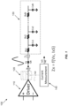
- FIG. 1 is a schematic diagram illustrating an example of an apparatus 100 for panel impedance sensing, within which some aspects of the subject technology are implemented.
- the apparatus 100 includes a driver circuit 110, a current sensor 120, a load 130 and a current-measurement circuit 140.
- the driver circuit 110 provides a voltage Vx at a node 128 of the load 130.
- the driver circuit 110 may include an amplifier and a buffer circuit.
- the current sensor 120 is an operational amplifier current sensor or a Hall-effect current sensor.
- the load 130 is a capacitive load that includes a distributed (lumped) resistor-capacitor (RC) circuit, as shown in FIG. 1 .
- RC distributed resistor-capacitor
- the load 130 includes a number of resistors Rx1, Rx2 ... RxN and a number of capacitors Cx1, Cx2 ... CxN, connected between end terminals of the respective resistors and the ground potential, as shown in FIG. 1 .
- the load 130 represent an impedance of a touch-sensitive layer of a touch-display panel of an electronic device.
- the current sensor 120 detects a current 122, which is measured by the current-measurement circuit 140.
- the current 122 is proportional to the current 112 (Ix) with a proportionality factor of K.
- the measured current 142 (IxS) is used to determine an impedance Zx of the load 130, as seen from the node 128.
- a node is an interconnection of two or more circuits or circuit element.
- the node 128 is an interconnection between the driver circuit 110 and the load 130.
- a load consists of one or more circuit elements that are connected to a circuit (e.g., the driver circuit 110) and receive, for example, energy or power from that circuit or draw a current from the circuit. This current is referred to as a load current.
- the subject disclosure implements the combination of the current sensor 120 and current-measurement circuit 140, as described herein, to enable panel impedance and/or bandwidth testing of the display panel by using minimal hardware. Further, the subject technology would allow taking into consideration the effects of the parasitic capacitor load at an output of the driver circuit 110.
- FIGs. 2A and 2B are schematic diagrams illustrating an example of an apparatus 200A for panel impedance sensing via a driver replica current and a corresponding chart 200B, respectively, according to aspects of the subject technology.
- the apparatus 200A may include an output stage of a transmit (TX) amplifier and uses a driver circuit 202 and a current measurement circuit 240.
- the driver circuit 202 is coupled to the panel 250 at a node 232 and provides a pixel current Ipix to the panel 250.
- the capacitor Cpar is a parasitic capacitor, which draws a current Ipar.
- the driver circuit 202 may further include a current sensor (similar to, for example, the current sensor 120 in FIG. 1 ).
- the driver circuit 202 further includes, but is not limited to, a circuit 210, a circuit 220 and an output stage 230.
- the circuit 210 is formed of p-type metal-oxide-semiconductor (PMOS) transistors and provides a current equal to Ip through the circuit 220, which also includes a direct-current (DC) current source Ios and switches S1 and S2.
- the circuit 220 may be characterized as a replica circuit that provides a replica current (Irep). In this regard, the circuit 220 is designed in part to replicate and match the current Ip.
- the replica current (Irep) is scaled by 1/N, but can subsequently be multiple by N to provide a replicated/matching current.
- the output stage 230 includes a pair of N-type MOS (NMOS) transistors and a switch S3. The output stage 230 provides a path for an alternate-current (AC) component of the current Ip to the ground.
- NMOS N-type MOS
- the current measurement circuit 240 is a circuit configured to provide a measurable voltage proportional to the current being measured.
- Current measurement circuit 240 may include a transimpedance amplifier (TIA) that generates a voltage based on a feedback loop into the current measurement circuit 240.
- TIA transimpedance amplifier
- the DC current source Ios is provided based on the switch S2 closing.
- Ios is a DC current with zero peak-to-peak (ptp) value
- Ipix ptp Ip ptp
- a ptp value (e.g., as shown in the plot 260) associated with the replica current (Irep) is equal (or proportional to, respectively) to a second ptp value associated with the load current (Ipix).
- the known frequency is the operating frequency of the TX amplifier.
- the measured sinusoidal voltage is converted to a digital signal, which, by using a known demodulation and fast-Fourier transform (FFT) operation, is converted to a ptp voltage value that is proportional to the ptp value of the replica current Irep.
- FFT fast-Fourier transform
- the ptp value of the Ipix which is the same as the ptp value of Ip (see Eq. 2) can be derived from the ptp value of the Irep.
- the DC current source Ios is considered part of the measurement error in the topology of FIG. 2 .
- the value of Cpar can be de-embedded, as shown in Fig.7 , by making two measurements, one measurement with S1 closed and the other one with both S1 and S2 closed.
- the driver circuit 202 provides the voltage Vtxp at the node 232 of the load (e.g., the panel 250).
- a first circuit e.g., circuit 210 and the circuit 220
- the load is a capacitive load and the first circuit facilitates determining the load current by measuring a replica current (e.g., Irep) and determining a capacitance of the load using values of the voltage and the replica current.
- the load includes at least a portion of a touch-display panel, and the load current (Ipix) is a pixel current associated with the touch-display panel.
- the voltage Vtxp is a periodic voltage (stimulus voltage), for example, with a sinusoidal waveform and a stimulus frequency.
- a periodic voltage can have a number of waveforms, for example, a sinusoidal waveform, a square waveform, a triangular waveform or other waveforms.
- the first circuit e.g., circuit 210 and the circuit 220
- the current measurement circuit 240 is a trans-impedance amplifier (TIA) circuit that provides a measurable voltage proportional to the replica current Irep at an output node 228 of the TIA.
- the current measurement circuit 240 facilitates extracting (determining) a single-pole RC model parameter associated with the load via measurements at different frequencies (e.g., two stimulus frequencies), as described herein.
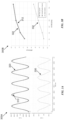
- the chart 200B includes plots 260, 262, 264 and 266.
- the plot 260 shows simulated time variation of the voltage at node 232.
- Plots 262, 264 and 266 depict simulated time variations of the load current Ipix, current Ip and the replica current Irep, respectively.
- the current load current Ipix has no DC value (due to no constant current value) and thus shows a ptp value.
- the current Ip has the bias current Ios component.
- a bias current is a DC current provided by a current source and used for biasing a circuit.
- FIGs. 3A and 3B are charts 300A and 300B illustrating simulated replica current and pixel currents, according to aspects of the subject technology.
- the chart 300A includes plots 310, 320 and 330.
- the plots 310 and 320 show time variations of the replica current Irep and the load current Ipix, respectively, which are generally similar and almost overlap one another.
- the plot 330 shows time variation of an error current, which is the difference between the plots 310 and 320, in an enlarged different scale and shows about 4% to 6% error between the measured Ireq and the load current Ipix.
- the error is due to the parasitic capacitance Cpar at the node 232 (shown in FIG. 2 ).
- the subject technology is designed calibrate and offset the effect of this capacitor, as discussed below.
- the chart 300B includes plots 312, 322 and 332.
- the plots 312 and 322 show frequency variations of the replica current Irep and the load current Ipix, respectively, which are generally similar and almost overlap one another.
- the plot 332 shows frequency variation of an error current, which is the difference between the plots 312 and 322, in an enlarged different scale between frequencies of 50 kilohertz (KHz) and 300 KHz.
- the charts 300A and 300B indicate the measured replica current Irep is a good match for the load current Ipix.
- FIG. 4 is a chart 400 illustrating a pixel total capacitance estimate, according to aspects of the subject technology.
- the chart 400 includes plots 410, 420 and 430 showing simulated pixel total impedances using a single pole model (RC), a lumped model two-pole model (RC-RC) and a distributed model, respectively. Below 100 KHz, which is good for capacitance measurement, the three models produce similar results.
- FIGs. 5A and 5B are charts 500A and 500B illustrating simulation result with a panel R/C sweep, according to aspects of the subject technology.
- the chart 500A includes plots 510 and 520 showing the total capacitance and the pixel capacitance, respectively.
- the plot 510 shows the total capacitance value versus variation (in %) of the pixel capacitance.
- the average value for the parasitic capacitance (Cpar) is seen to be about 47 picofarad (pF).
- the charts 500A and 500B are the result of testing the effectiveness of the single-pole approximation measurement.
- the chart 500A shows the measured value of Cpix increasing as we sweep Cpix.
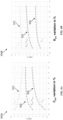
- FIGs. 6A and 6B are charts 600A and 600B illustrating total load capacitance extraction using a single measurement, according to aspects of the subject technology.
- the chart 600A includes plots 610, 620 and 630, showing errors (%) in values of Cpix, Cpix*Rpix and Rpix, respectively, versus Cpix variation (%).
- the chart 600B includes plots 612, 622 and 632, showing errors (%) in values of Cpix, Cpix*Rpix and Rpix, respectively, versus Rpix variation (%).
- the charts 600A and 600B are simulation results of a one-time measurement and indicate that, given manufacturer variation on R or C of [-40% to 40%], the measured RC accuracy by the implemented circuit is within two percent.
- FIG. 7 is a schematic diagram illustrating an example of a circuit 700 for an improved impedance estimate via pixel load reconfiguration, according to aspects of the subject technology.
- the circuit 700 is a load-reconfiguration circuit that is used to remove an effect of a parasitic capacitance Cpar (e.g., Cpar of FIG. 2A ) at an output node of the first circuit from a measured replica current (e.g., Irep of FIG. 2A ).
- the circuit 700 includes an amplifier 710, switches S 1 and S 2 , pixel resistors R pix1 and R pix2 and pixel capacitances C pix1 and C pix2 .
- the parasitic capacitance Cpar is not part of the single-model RC parameter discussed above.
- I pix 2 I m 2 ⁇ I m 1
- the pixel current I pix1 can be obtained similarly.
- FIGs. 8A and 8B are charts 800A and 800B illustrating simulation result with panel Rpix and Cpix sweep, according to aspects of the subject technology.
- the chart 800A includes plots 810, 820 and 830 showing errors (%) in values of Rpix, Cpix*Rpix and Cpix, respectively, versus Cpix variation (%).
- the chart 800B includes plots 812, 822 and 832 illustrating errors (%) in values of Rpix, Cpix*Rpix and Cpix, respectively, versus Rpix variation (%).
- the charts 700A and 700B indicate measurement error with a two-measurements method. The absolute measurement error on Cpix is improved from 8% (in 600A and 600B) to 0.1% (in 700A and 700B).
- FIG. 9 is a flow diagram illustrating an example of a process 900 for panel impedance sensing via a driver replica current, according to aspects of the subject technology.
- the process 900 includes providing a voltage at a node (e.g., node 232 of FIG. 2A ) of a load (e.g., panel 250 of FIG. 2A ) using a driver (e.g., driver circuit 202 of FIG. 2A ) (block 910).
- the process 900 also includes determining a load current (e.g., pixel current Ipix of FIG. 2A ) at the node by measuring a replica current (e.g., replica current Irep of FIG.
- a load current e.g., pixel current Ipix of FIG. 2A
- the process 900 further includes determining a capacitance (e.g., C pix of FIG. 5A ) of the load using values of the voltage and the replica current (block 930)
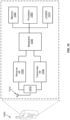
- FIG. 10 illustrates an example of a wireless communication device 1000, within which some aspects of the subject technology are implemented.
- the wireless communication device 1000 can be a laptop computer, a desktop computer, a tablet, a smart TV, a smartphone, a smartwatch or other electronic devices, including one or more health-sense device(s).
- the wireless communication device 1000 may comprise an RF antenna 1010, a duplexer 1012, a receiver 1020, a transmitter 1030, a baseband processing module 1040, a memory 1050, a processor 1060 and a local oscillator generator (LOGEN) 1070.
- LOGEN local oscillator generator
- one or more of the blocks represented in FIG. 10 may be integrated on one or more semiconductor substrates.
- blocks 1020-1070 may be realized in a single chip, a single system on a chip or in a multichip chipset.
- the receiver 1020 may comprise suitable logic circuitry and/or code that may be operable to receive and process signals from the RF antenna 1010.
- the receiver 1020 may, for example, be operable to amplify and/or down convert received wireless signals.
- the receiver 1020 may be operable to cancel noise in received signals, and may be linear over a wide range of frequencies. In this manner, the receiver 1020 may be suitable for receiving signals in accordance with a variety of wireless standards, such as Wi-Fi, WiMAX, BT and various cellular standards.
- the receiver 1020 may not use any sawtooth acoustic wave filters, and a few or no off-chip discrete components such as large capacitors and inductors.
- the transmitter 1030 may comprise suitable logic circuitry and/or code that may be operable to process and transmit signals from the RF antenna 1010.
- the transmitter 1030 may, for example, be operable to upconvert baseband signals to RF signals and amplify RF signals.
- the transmitter 1030 may be operable to upconvert and amplify baseband signals processed in accordance with a variety of wireless standards. Examples of such standards may include Wi-Fi, WiMAX, BT and various cellular standards.
- the transmitter 1030 may be operable to provide signals for further amplification by one or more power amplifiers.
- the duplexer 1012 may provide isolation in the transmit band to avoid saturation of the receiver 1020 or damaging parts of the receiver 1020, and to relax one or more design requirements of the receiver 1020. Furthermore, the duplexer 1012 may attenuate the noise in the receiver band. The duplexer 1012 may be operable in multiple frequency bands of various wireless standards.
- the baseband processing module 1040 may comprise suitable logic, circuitry, interfaces and/or code that may be operable to perform the processing of baseband signals.
- the baseband processing module 1040 may, for example, analyze received signals, generate control and/or feedback signals for configuring various components of the wireless communication device 1000, such as the receiver 1020.
- the baseband processing module 1040 may be operable to encode, decode, transcode, modulate, demodulate, encrypt, decrypt, scramble, descramble and/or otherwise process data in accordance with one or more wireless standards.
- the processor 1060 may comprise suitable logic, circuitry and/or code that may enable processing data and/or controlling operations of the wireless communication device 1000.
- the processor 1060 may be enabled to provide control signals to various other portions of the wireless communication device 1000.
- the processor 1060 may also control the transfer of data between various portions of the wireless communication device 1000.
- the processor 1060 may enable implementation of an OS, or otherwise execute code to manage operations of the wireless communication device 1000.
- the processor 1060 may be interfaced with transducer modules via existing host interface technologies such as an inter-integrated circuit (I2C), a serial interface protocol (SPI), a peripheral component interconnect express (PCIE), a universal asynchronous receiver-transmitter (UART) and/or other interface technologies, depending on the data rate needed to sample and pipe from the transducers module to the processor 1060.
- I2C inter-integrated circuit
- SPI serial interface protocol
- PCIE peripheral component interconnect express
- UART universal asynchronous receiver-transmitter
- the memory 1050 may comprise suitable logic, circuitry and/or code that may enable storage of various types of information such as received data, generated data, code and/or configuration information.
- the memory 1050 may comprise, for example, RAM, ROM, flash and/or magnetic storage. In various aspects of the subject technology, information stored in the memory 1050 may be utilized for configuring the receiver 1020 and/or the baseband processing module 1040.
- the LOGEN 1070 may comprise suitable logic, circuitry, interfaces and/or code that may be operable to generate one or more oscillating signals of one or more frequencies.
- the LOGEN 1070 may be operable to generate digital and/or analog signals. In this manner, the LOGEN 1070 may be operable to generate one or more clock signals and/or sinusoidal signals. Characteristics of the oscillating signals, such as the frequency and duty cycle, may be determined based on one or more control signals from, for example, the processor 1060 and/or the baseband processing module 1040.
- the processor 1060 may configure the various components of the wireless communication device 1000 based on a wireless standard, according to which it is designed to receive signals.
- Wireless signals may be received via the RF antenna 1010, amplified, and down converted by the receiver 1020.
- the baseband processing module 1040 may perform noise estimation and/or noise cancellation, decoding and/or demodulation of the baseband signals. In this manner, information in the received signal may be recovered and utilized appropriately.
- the information may be audio and/or video to be presented to a user of the wireless communication device 1000, data to be stored to the memory 1050 and/or information affecting and/or enabling operation of the wireless communication device 1000.
- the baseband processing module 1040 may modulate, encode and perform other processing on audio, video and/or control signals to be transmitted by the transmitter 1030 in accordance with various wireless standards.
- the techniques of the subject technology can be utilized to measure panel impedance of a touch-display panel of the wireless communication device 1000 (not shown in FIG. 10 for simplicity) via a driver replica current (e.g., Irep of FIG. 2A ), as discussed above.
- a driver replica current e.g., Irep of FIG. 2A
- a processor configured to monitor and control an operation or a component may also mean the processor is being programmed to monitor and control the operation, or the processor being operable to monitor and control the operation.
- a processor configured to execute code can be construed as a processor programmed or operable to execute code.
- a phrase such as an "aspect” does not imply that such aspect is essential to the subject technology or that such aspect applies to all configurations of the subject technology.
- a disclosure relating to an aspect may apply to all configurations or one or more configurations.
- a phrase such as an “aspect” may refer to one or more aspects, and vice versa.
- a phrase such as a “configuration” does not imply that such configuration is essential to the subject technology or that such configuration applies to all configurations of the subject technology.
- a disclosure relating to a configuration may apply to all configurations or one or more configurations.
- a phrase such as a "configuration” may refer to one or more configurations, and vice versa.
- example is used herein to mean “serving as an example or illustration.” Any aspect or design described herein as an “example” is not necessarily to be construed as preferred or advantageous over other aspects or designs.
Landscapes
- Engineering & Computer Science (AREA)
- Physics & Mathematics (AREA)
- General Physics & Mathematics (AREA)
- General Engineering & Computer Science (AREA)
- Theoretical Computer Science (AREA)
- Human Computer Interaction (AREA)
- Measurement Of Resistance Or Impedance (AREA)
Abstract
Description
- The present description relates generally to electronic circuits, including, for example, panel impedance sensing via driver replica current.
- Many electronic displays, including displays of the electronic devices, for example, consumer electronic devices, laptops, hand-held electronic devices such as tablets and phones and smartwatches, use display panels formed of a two-dimensional sensor array. The sensor arrays are implemented as two or more layers formed over a cover glass. The sensor arrays are typically modeled with a two-dimensional distributed resistor-capacitor (RC) circuits that are powered by driver circuits. For example, an N by M pixel-array panel is formed by a two-dimensional array of M*N pixels, and each pixel is represented by an RC circuit. The resistors of each row or column are serially connected to one another, and the capacitors are connected between successive resistors and a ground potential. The N by M pixel-array panel can be powered, for example, by N horizontal drivers and M vertical drivers.
- Certain features of the subject technology are set forth in the appended claims. However, for purposes of explanation, several aspects of the subject technology are depicted in the following figures:
-
FIG. 1 is a schematic diagram illustrating an example of a circuit for panel impedance sensing, within which some aspects of the subject technology are implemented. -
FIGs. 2A and 2B are schematic diagrams illustrating an example of a circuit for panel impedance sensing via a driver replica current and a corresponding chart, according to aspects of the subject technology. -
FIGs. 3A and 3B are charts illustrating simulated replica and pixel currents, according to aspects of the subject technology. -
FIG. 4 is a chart illustrating a pixel total capacitance estimate, according to aspects of the subject technology. -
FIGs. 5A and 5B are charts illustrating simulation result with a panel R/C sweep, according to aspects of the subject technology. -
FIGs. 6A and 6B are charts illustrating total load capacitance extraction using a single measurement, according to aspects of the subject technology. -
FIG. 7 is a schematic diagram illustrating an example of a circuit for an improved impedance estimate via pixel load reconfiguration, according to aspects of the subject technology. -
FIGs. 8A and 8B are charts illustrating simulation result with panel Cpix and Rpix sweep, according to aspects of the subject technology. -
FIG. 9 is a flow diagram illustrating an example of a process for panel impedance sensing via a driver replica current, according to aspects of the subject technology. -
FIG. 10 illustrates an example of a wireless communication device, within which some aspects of the subject technology are implemented. - The detailed description set forth below is intended as a description of various configurations of the subject technology and is not intended to represent the only configurations in which the subject technology may be practiced. The appended drawings are incorporated herein, and constitute a part of the detailed description. The detailed description includes specific details for the purpose of providing a thorough understanding of the subject technology. However, the subject technology is not limited to the specific details set forth herein and may be practiced using one or more implementations. In one or more instances, structures and components are shown in block diagram form in order to avoid obscuring the concepts of the subject technology.
- According to some aspects, the subject technology is directed to panel impedance sensing via a driver replica current. The panel may include a touch-display panel formed of an N by M array of resistor-capacitor (RC) circuits. The touch-display panel can be used in an electronic device, for example, a consumer electronic device, a laptop computer, a desktop computer, a smart TV, a hand-held electronic device such as a tablet and a phone, a smartwatch and similar devices. The subject technology allows panel impedance and/or bandwidth testing using minimal hardware. The disclosed technique drives the pixels with a stimulus voltage (Vpix) and measures a pixel current (Ipix) using a replica current. In some embodiments, a pixel current is the current drawn by a pixel of a display panel from a corresponding driver circuit. A single measurement can provide an estimate of a total load capacitance. Using two different frequencies, the subject technology computes a single-pole RC approximation. Using additional measurements allows extracting higher order model parameters, as further discussed herein. The technique of subject technology allows taking into account parasitic capacitor load at an output of the driver.
- In some embodiments, a circuit of the subject technology includes a driver to provide a voltage at a node of a load and a first circuit to facilitate determining a load current at the node. The load is a capacitive load, and the first circuit facilitates determining the load current by measuring a replica current and determining a capacitance of the load using values of the voltage and the replica current.
- In some embodiments, a circuit for impedance sensing includes a driver to provide a voltage at a node of a panel. A first circuit coupled to the node facilitates measuring a replica current and determining an admittance of the panel at the node by using the replica current and the voltage. In some embodiments, the admittance is a capacitive admittance. In some embodiments, a capacitive admittance refers to the admittance of a circuit that is formed by interconnection of two or more capacitors or can be reduced to an equivalent circuit including one or more capacitors.
- In some embodiments, a communication device includes a display panel and a driver to provide a voltage at a node of the display panel. A first circuit is coupled to the node to facilitate measuring a replica current and determining a capacitance of the display panel by using peak-to-peak values of the voltage and the replica current, as described in more details herein.
-
FIG. 1 is a schematic diagram illustrating an example of anapparatus 100 for panel impedance sensing, within which some aspects of the subject technology are implemented. Theapparatus 100 includes adriver circuit 110, acurrent sensor 120, aload 130 and a current-measurement circuit 140. In some embodiments, thedriver circuit 110 provides a voltage Vx at anode 128 of theload 130. In some embodiments, thedriver circuit 110 may include an amplifier and a buffer circuit. In some embodiments, thecurrent sensor 120 is an operational amplifier current sensor or a Hall-effect current sensor. In some embodiments, theload 130 is a capacitive load that includes a distributed (lumped) resistor-capacitor (RC) circuit, as shown inFIG. 1 . For example, theload 130 includes a number of resistors Rx1, Rx2 ... RxN and a number of capacitors Cx1, Cx2 ... CxN, connected between end terminals of the respective resistors and the ground potential, as shown inFIG. 1 . In some embodiments, theload 130 represent an impedance of a touch-sensitive layer of a touch-display panel of an electronic device. Thecurrent sensor 120 detects a current 122, which is measured by the current-measurement circuit 140. The current 122 is proportional to the current 112 (Ix) with a proportionality factor of K. The measured current 142 (IxS) is used to determine an impedance Zx of theload 130, as seen from thenode 128. In the context of the subject disclosure, a node is an interconnection of two or more circuits or circuit element. For example, thenode 128 is an interconnection between thedriver circuit 110 and theload 130. In the context of the subject disclosure, a load consists of one or more circuit elements that are connected to a circuit (e.g., the driver circuit 110) and receive, for example, energy or power from that circuit or draw a current from the circuit. This current is referred to as a load current. The impedance Zx is a function (f) of the voltage Vx and the measured current 142 (IsX) and can be expressed as: Zx = f (Vx, IsX). - The subject disclosure implements the combination of the
current sensor 120 and current-measurement circuit 140, as described herein, to enable panel impedance and/or bandwidth testing of the display panel by using minimal hardware. Further, the subject technology would allow taking into consideration the effects of the parasitic capacitor load at an output of thedriver circuit 110. -
FIGs. 2A and 2B are schematic diagrams illustrating an example of anapparatus 200A for panel impedance sensing via a driver replica current and acorresponding chart 200B, respectively, according to aspects of the subject technology. Theapparatus 200A may include an output stage of a transmit (TX) amplifier and uses adriver circuit 202 and acurrent measurement circuit 240. Thedriver circuit 202 is coupled to thepanel 250 at anode 232 and provides a pixel current Ipix to thepanel 250. The capacitor Cpar is a parasitic capacitor, which draws a current Ipar. Thedriver circuit 202 may further include a current sensor (similar to, for example, thecurrent sensor 120 inFIG. 1 ). Thedriver circuit 202 further includes, but is not limited to, acircuit 210, acircuit 220 and anoutput stage 230. Thecircuit 210 is formed of p-type metal-oxide-semiconductor (PMOS) transistors and provides a current equal to Ip through thecircuit 220, which also includes a direct-current (DC) current source Ios and switches S1 and S2. Thecircuit 220 may be characterized as a replica circuit that provides a replica current (Irep). In this regard, thecircuit 220 is designed in part to replicate and match the current Ip. The replica current (Irep) is scaled by 1/N, but can subsequently be multiple by N to provide a replicated/matching current. Theoutput stage 230 includes a pair of N-type MOS (NMOS) transistors and a switch S3. Theoutput stage 230 provides a path for an alternate-current (AC) component of the current Ip to the ground. - In a configuration operation, when the switches S1 and S2 are closed, the replica current (Irep) from the
circuit 220 is provided to thecurrent measurement circuit 240. In some embodiments, thecurrent measurement circuit 240 is a circuit configured to provide a measurable voltage proportional to the current being measured.Current measurement circuit 240 may include a transimpedance amplifier (TIA) that generates a voltage based on a feedback loop into thecurrent measurement circuit 240. Also, the DC current source Ios is provided based on the switch S2 closing. Also, when the switch S3 is opened, the current In of theoutput stage 230 is set equal to zero. In this configuration, if the parasitic capacitance Cpar and the corresponding current Ipar are ignored, the current Ipix is given as:
- Considering that Ios is a DC current with zero peak-to-peak (ptp) value,

- Because Ip is equal to (or proportional to) the replica current (Irep), a ptp value (e.g., as shown in the plot 260) associated with the replica current (Irep) is equal (or proportional to, respectively) to a second ptp value associated with the load current (Ipix).
- From this, the admittance Y of the
panel 250 can be obtained:
node 232, and the ptp value of Ip is the same as the ptp value of replica current Irep, which is converted to a sinusoidal voltage with a known frequency at anoutput node 228 of thecurrent measurement circuit 240. The known frequency is the operating frequency of the TX amplifier. The measured sinusoidal voltage is converted to a digital signal, which, by using a known demodulation and fast-Fourier transform (FFT) operation, is converted to a ptp voltage value that is proportional to the ptp value of the replica current Irep. Then, the ptp value of the Ipix, which is the same as the ptp value of Ip (see Eq. 2) can be derived from the ptp value of the Irep. The DC current source Ios is considered part of the measurement error in the topology ofFIG. 2 . The value of Cpar can be de-embedded, as shown inFig.7 , by making two measurements, one measurement with S1 closed and the other one with both S1 and S2 closed. - In some embodiments, the
driver circuit 202 provides the voltage Vtxp at thenode 232 of the load (e.g., the panel 250). In some embodiments, a first circuit (e.g.,circuit 210 and the circuit 220) facilitate determining a load current (e.g., Ipix) at thenode 232. The load is a capacitive load and the first circuit facilitates determining the load current by measuring a replica current (e.g., Irep) and determining a capacitance of the load using values of the voltage and the replica current. In some embodiments, the load includes at least a portion of a touch-display panel, and the load current (Ipix) is a pixel current associated with the touch-display panel. In some embodiments, the voltage Vtxp is a periodic voltage (stimulus voltage), for example, with a sinusoidal waveform and a stimulus frequency. In general, a periodic voltage can have a number of waveforms, for example, a sinusoidal waveform, a square waveform, a triangular waveform or other waveforms. In some embodiments, the first circuit (e.g.,circuit 210 and the circuit 220) includes a bias-current source (Ios) andcircuit 210 provide the replica current (Irep) to acurrent measurement circuit 240. - In some embodiments, the
current measurement circuit 240 is a trans-impedance amplifier (TIA) circuit that provides a measurable voltage proportional to the replica current Irep at anoutput node 228 of the TIA. In some embodiments, thecurrent measurement circuit 240 facilitates extracting (determining) a single-pole RC model parameter associated with the load via measurements at different frequencies (e.g., two stimulus frequencies), as described herein. - The
chart 200B includesplots plot 260 shows simulated time variation of the voltage atnode 232.Plots plot 264, the current load current Ipix has no DC value (due to no constant current value) and thus shows a ptp value. The current Ip has the bias current Ios component. In some embodiments, a bias current is a DC current provided by a current source and used for biasing a circuit. -
FIGs. 3A and 3B arecharts chart 300A includesplots plots plot 330 shows time variation of an error current, which is the difference between theplots FIG. 2 ). The subject technology is designed calibrate and offset the effect of this capacitor, as discussed below. - The
chart 300B includesplots plots 312 and 322 show frequency variations of the replica current Irep and the load current Ipix, respectively, which are generally similar and almost overlap one another. Theplot 332 shows frequency variation of an error current, which is the difference between theplots 312 and 322, in an enlarged different scale between frequencies of 50 kilohertz (KHz) and 300 KHz. Thecharts -
FIG. 4 is achart 400 illustrating a pixel total capacitance estimate, according to aspects of the subject technology. Thechart 400 includesplots -
FIGs. 5A and 5B arecharts chart 500A includesplots 
- The
plot 510 shows the total capacitance value versus variation (in %) of the pixel capacitance. The difference in capacitance values, as shown in theplots plot 530 of thechart 500B. The average value for the parasitic capacitance (Cpar) is seen to be about 47 picofarad (pF). Thecharts chart 500A shows the measured value of Cpix increasing as we sweep Cpix. Thechart 500B shows the subtracted value, Cpar = Ctotal - Cpix, given the Cpix variation. - In some aspects, the single-pole RC model parameters can be extracted (determined) from two measurements at two different stimulus frequencies ω1 (e.g., 2π*100 KHz) and ω2 (e.g., 2π*300 KHz) as follows:


plot 410 ofFIG. 4 . -
FIGs. 6A and 6B arecharts chart 600A includesplots chart 600B includesplots charts -
FIG. 7 is a schematic diagram illustrating an example of acircuit 700 for an improved impedance estimate via pixel load reconfiguration, according to aspects of the subject technology. In some embodiments, thecircuit 700 is a load-reconfiguration circuit that is used to remove an effect of a parasitic capacitance Cpar (e.g., Cpar ofFIG. 2A ) at an output node of the first circuit from a measured replica current (e.g., Irep ofFIG. 2A ). Thecircuit 700 includes anamplifier 710, switches S1 and S2, pixel resistors Rpix1 and Rpix2 and pixel capacitances Cpix1 and Cpix2. The parasitic capacitance Cpar is not part of the single-model RC parameter discussed above. Thecircuit 700 is used to measure pixel currents (Ipix1 or Ipix2) by eliminating the effect of the parasitic capacitance Cpar in three steps. First, switch S1 is closed while switch S2 is open and a first measured current (Im1) is obtained which is:
- Second, switches S1 and S2 are closed and a second measured current (Im2) is obtained which is:

- Third, Im1 is subtracted from Im2 to obtain Ipix2:

- The pixel current Ipix1 can be obtained similarly.
-
FIGs. 8A and 8B arecharts chart 800A includesplots chart 800B includesplots -
FIG. 9 is a flow diagram illustrating an example of aprocess 900 for panel impedance sensing via a driver replica current, according to aspects of the subject technology. Theprocess 900 includes providing a voltage at a node (e.g.,node 232 ofFIG. 2A ) of a load (e.g.,panel 250 ofFIG. 2A ) using a driver (e.g.,driver circuit 202 ofFIG. 2A ) (block 910). Theprocess 900 also includes determining a load current (e.g., pixel current Ipix ofFIG. 2A ) at the node by measuring a replica current (e.g., replica current Irep ofFIG. 2A ) using a first circuit (e.g.,circuit 210 and thecircuit 220 ofFIG. 2A ) (block 920). Theprocess 900 further includes determining a capacitance (e.g., Cpix ofFIG. 5A ) of the load using values of the voltage and the replica current (block 930) -
FIG. 10 illustrates an example of awireless communication device 1000, within which some aspects of the subject technology are implemented. In one or more implementations, thewireless communication device 1000 can be a laptop computer, a desktop computer, a tablet, a smart TV, a smartphone, a smartwatch or other electronic devices, including one or more health-sense device(s). Thewireless communication device 1000 may comprise anRF antenna 1010, aduplexer 1012, areceiver 1020, atransmitter 1030, abaseband processing module 1040, amemory 1050, aprocessor 1060 and a local oscillator generator (LOGEN) 1070. In various aspects of the subject technology, one or more of the blocks represented inFIG. 10 may be integrated on one or more semiconductor substrates. For example, blocks 1020-1070 may be realized in a single chip, a single system on a chip or in a multichip chipset. - The
receiver 1020 may comprise suitable logic circuitry and/or code that may be operable to receive and process signals from theRF antenna 1010. Thereceiver 1020 may, for example, be operable to amplify and/or down convert received wireless signals. In various aspects of the subject technology, thereceiver 1020 may be operable to cancel noise in received signals, and may be linear over a wide range of frequencies. In this manner, thereceiver 1020 may be suitable for receiving signals in accordance with a variety of wireless standards, such as Wi-Fi, WiMAX, BT and various cellular standards. In various aspects of the subject technology, thereceiver 1020 may not use any sawtooth acoustic wave filters, and a few or no off-chip discrete components such as large capacitors and inductors. - The
transmitter 1030 may comprise suitable logic circuitry and/or code that may be operable to process and transmit signals from theRF antenna 1010. Thetransmitter 1030 may, for example, be operable to upconvert baseband signals to RF signals and amplify RF signals. In various aspects of the subject technology, thetransmitter 1030 may be operable to upconvert and amplify baseband signals processed in accordance with a variety of wireless standards. Examples of such standards may include Wi-Fi, WiMAX, BT and various cellular standards. In various aspects of the subject technology, thetransmitter 1030 may be operable to provide signals for further amplification by one or more power amplifiers. - The
duplexer 1012 may provide isolation in the transmit band to avoid saturation of thereceiver 1020 or damaging parts of thereceiver 1020, and to relax one or more design requirements of thereceiver 1020. Furthermore, theduplexer 1012 may attenuate the noise in the receiver band. Theduplexer 1012 may be operable in multiple frequency bands of various wireless standards. - The
baseband processing module 1040 may comprise suitable logic, circuitry, interfaces and/or code that may be operable to perform the processing of baseband signals. Thebaseband processing module 1040 may, for example, analyze received signals, generate control and/or feedback signals for configuring various components of thewireless communication device 1000, such as thereceiver 1020. Thebaseband processing module 1040 may be operable to encode, decode, transcode, modulate, demodulate, encrypt, decrypt, scramble, descramble and/or otherwise process data in accordance with one or more wireless standards. - The
processor 1060 may comprise suitable logic, circuitry and/or code that may enable processing data and/or controlling operations of thewireless communication device 1000. In this regard, theprocessor 1060 may be enabled to provide control signals to various other portions of thewireless communication device 1000. Theprocessor 1060 may also control the transfer of data between various portions of thewireless communication device 1000. Additionally, theprocessor 1060 may enable implementation of an OS, or otherwise execute code to manage operations of thewireless communication device 1000. In one or more implementations, theprocessor 1060 may be interfaced with transducer modules via existing host interface technologies such as an inter-integrated circuit (I2C), a serial interface protocol (SPI), a peripheral component interconnect express (PCIE), a universal asynchronous receiver-transmitter (UART) and/or other interface technologies, depending on the data rate needed to sample and pipe from the transducers module to theprocessor 1060. - The
memory 1050 may comprise suitable logic, circuitry and/or code that may enable storage of various types of information such as received data, generated data, code and/or configuration information. Thememory 1050 may comprise, for example, RAM, ROM, flash and/or magnetic storage. In various aspects of the subject technology, information stored in thememory 1050 may be utilized for configuring thereceiver 1020 and/or thebaseband processing module 1040. - The
LOGEN 1070 may comprise suitable logic, circuitry, interfaces and/or code that may be operable to generate one or more oscillating signals of one or more frequencies. TheLOGEN 1070 may be operable to generate digital and/or analog signals. In this manner, theLOGEN 1070 may be operable to generate one or more clock signals and/or sinusoidal signals. Characteristics of the oscillating signals, such as the frequency and duty cycle, may be determined based on one or more control signals from, for example, theprocessor 1060 and/or thebaseband processing module 1040. - In operation, the
processor 1060 may configure the various components of thewireless communication device 1000 based on a wireless standard, according to which it is designed to receive signals. Wireless signals may be received via theRF antenna 1010, amplified, and down converted by thereceiver 1020. Thebaseband processing module 1040 may perform noise estimation and/or noise cancellation, decoding and/or demodulation of the baseband signals. In this manner, information in the received signal may be recovered and utilized appropriately. For example, the information may be audio and/or video to be presented to a user of thewireless communication device 1000, data to be stored to thememory 1050 and/or information affecting and/or enabling operation of thewireless communication device 1000. Thebaseband processing module 1040 may modulate, encode and perform other processing on audio, video and/or control signals to be transmitted by thetransmitter 1030 in accordance with various wireless standards. - In some implementations, the techniques of the subject technology can be utilized to measure panel impedance of a touch-display panel of the wireless communication device 1000 (not shown in
FIG. 10 for simplicity) via a driver replica current (e.g., Irep ofFIG. 2A ), as discussed above. - The predicate words "configured to," "operable to" and "programmed to" do not imply any particular tangible or intangible modification of a subject, but rather are intended to be used interchangeably. For example, a processor configured to monitor and control an operation or a component may also mean the processor is being programmed to monitor and control the operation, or the processor being operable to monitor and control the operation. Likewise, a processor configured to execute code can be construed as a processor programmed or operable to execute code.
- A phrase such as an "aspect" does not imply that such aspect is essential to the subject technology or that such aspect applies to all configurations of the subject technology. A disclosure relating to an aspect may apply to all configurations or one or more configurations. A phrase such as an "aspect" may refer to one or more aspects, and vice versa. A phrase such as a "configuration" does not imply that such configuration is essential to the subject technology or that such configuration applies to all configurations of the subject technology. A disclosure relating to a configuration may apply to all configurations or one or more configurations. A phrase such as a "configuration" may refer to one or more configurations, and vice versa.
- The word "example" is used herein to mean "serving as an example or illustration." Any aspect or design described herein as an "example" is not necessarily to be construed as preferred or advantageous over other aspects or designs.
- When an element is referred to herein as being "connected" or "coupled" to another element, it is to be understood that the elements can be directly connected to the other element, or have intervening elements present between the elements. In contrast, when an element is referred to as being "directly connected" or "directly coupled" to another element, it should be understood that no intervening elements are present in the "direct" connection between the elements. However, the existence of a direct connection does not exclude other connections, in which intervening elements may be present.
- When a quantity is referred to herein as being "equal" or "proportional" to another quantity, it is to be understood that in engineering the quantities may not have absolutely accurate values due to a number of factors, which allow for reasonable deviations due to, for example, margins of error, tolerances, interferences, and other engineering realities.
- All structural and functional equivalents to the elements of the various aspects described throughout this disclosure that are known, or later come to be known to those of ordinary skill in the art, are expressly incorporated herein by reference and are intended to be encompassed by the claims. Moreover, nothing disclosed herein is intended to be dedicated to the public, regardless of whether such disclosure is explicitly recited in the claims. No claim element is to be construed under the provisions of 35 U.S.C. §112(f) unless the element is expressly recited using the phrase "means for" or, in the case of a method claim, the element is recited using the phrase "step for." Furthermore, to the extent that the term "include," "have" or the like is used in the description or the claims, such term is intended to be inclusive in a manner similar to the term "comprise," as "comprise" is interpreted when employed as a transitional word in a claim.
- Those of skill in the art would appreciate that the various illustrative blocks, modules, elements, components, methods and algorithms described herein may be implemented as electronic hardware, computer software or combinations of both. To illustrate this interchangeability of hardware and software, various illustrative blocks, modules, elements, components, methods and algorithms have been described above, generally in terms of their functionality. Whether such functionality is implemented as hardware or software depends upon the particular application, and design constraints imposed on the overall system. Skilled artisans may implement the described functionality in varying ways for each particular application. Various components and blocks may be arranged differently (e.g., arranged in a different order or partitioned in a different way), all without departing from the scope of the subject technology.
Claims (15)
- An apparatus, comprising:a driver circuit configured to provide a voltage at a node of a load, the voltage based on a first current;a first circuit configured to generate a second current proportional to the first current; anda second circuit configured to measure the first current by:measuring the second current; anddetermining a capacitance of the load using values of voltage and the second current.
- The apparatus of claim 1, wherein:the load comprises at least a portion of a touch-display panel, andthe first current comprises a pixel current provided to the touch-display panel.
- The apparatus of claim 1 or 2, wherein
the voltage comprises a voltage having a sinusoidal waveform. - The apparatus of any one of the claims 1 to 3, wherein
the voltage comprises a peak-to-peak voltage. - The apparatus of any one of the claims 1 to 4, whereinthe second current comprises a first peak-to-peak value, andthe first current comprises a load current comprising a second peak-to-peak value equal to the first peak-to-peak value.
- The apparatus of any one of the claims 1 to 5, wherein
the first circuit comprises a bias-current source configured to provide the second current. - The apparatus of any one of the claims 1 to 6, further comprisinga current measurement circuit configured to provide a measurable voltage proportional to the second current;wherein in particularthe current measurement circuit is configured todetermine a resistance-capacitance (RC) model parameter associated with the load via measurements at different frequencies, andthe different frequencies are used to determine the capacitance;wherein further in particularthe current measurement circuit comprises a trans-impedance amplifier circuit configured to provide the measurable voltage.
- The apparatus of any one of the claims 1 to 7, further comprising
a load-reconfiguration circuit configured to remove an effect of a parasitic capacitance of the first circuit. - A circuit for impedance sensing, the circuit comprising:a driver circuit configured to provide a voltage at a node, the voltage being based on a first circuit configured to generate a third current based on the first circuit, anda second circuit coupled to the node, the second circuit configured to:measure the third current; anddetermining an admittance at the node by using the third current and the voltage.
- The circuit of claim 9, wherein
the admittance comprises a capacitive admittance, and the node is part of a touch-display panel. - The circuit of claim 9 or 10, wherein
the second circuit is configured to determine the admittance by using peak-to-peak values of the third current and the voltage. - The circuit of any one of the claims 9 to 11, whereinthe second circuit comprises a bias-current source configured to provide the third current; wherein in particularthe circuit further comprises
a trans-impedance amplifier circuit configured to provide a measurable voltage proportional to the third current;wherein further in particularthe voltage comprises a stimulus voltage configured to electrically stimulate a third circuit coupled to the driver circuit at the node and operating at a frequency, andthe admittance is based on the frequency. - The circuit of any one of the claims 9 to 12, further comprising
a load-reconfiguration circuit configured to remove a parasitic capacitance of the first circuit. - An apparatus, comprising:a display panel;a first circuit configured to provide a voltage at a node of the display panel, wherein the voltage is based on a first current; anda second circuit coupled to the node and configured to:receive a second current proportional to the first current.determine a value of the second current; anddetermine a capacitance of the display panel by using peak-to-peak values of the voltage and the second current.
- The apparatus of claim 14, further comprising
a current-measurement circuit, wherein:the second circuit comprises a bias-current source configured to provide the second current to the current-measurement circuit,the current-measurement circuit is configured to determine the value of the second current by providing a measurable voltage proportional to the second current;wherein in particularthe current-measurement circuit comprises a trans-impedance amplifier circuit configured to provide the measurable voltage.
Applications Claiming Priority (1)
| Application Number | Priority Date | Filing Date | Title |
|---|---|---|---|
| US18/122,061 US12392811B2 (en) | 2023-03-15 | 2023-03-15 | Panel impedance sensing via driver replica current |
Publications (2)
| Publication Number | Publication Date |
|---|---|
| EP4432059A1 true EP4432059A1 (en) | 2024-09-18 |
| EP4432059B1 EP4432059B1 (en) | 2025-12-31 |
Family
ID=90362873
Family Applications (1)
| Application Number | Title | Priority Date | Filing Date |
|---|---|---|---|
| EP24162129.1A Active EP4432059B1 (en) | 2023-03-15 | 2024-03-07 | PCB IMPEDANCE MEASUREMENT VIA DRIVER REPLICA POWER |
Country Status (4)
| Country | Link |
|---|---|
| US (1) | US12392811B2 (en) |
| EP (1) | EP4432059B1 (en) |
| CN (1) | CN118675436A (en) |
| ES (1) | ES3066622T3 (en) |
Citations (2)
| Publication number | Priority date | Publication date | Assignee | Title |
|---|---|---|---|---|
| US20190257870A1 (en) * | 2018-02-16 | 2019-08-22 | Rohm Co., Ltd. | Capacitance detection circuit, semiconductor device, input device and electronic apparatus including the same, and method of detecting capacitance |
| US20220011891A1 (en) * | 2020-03-27 | 2022-01-13 | Shenzhen GOODIX Technology Co., Ltd. | Capacitance detecting circuit, touch control chip, touch detection apparatus and electronic device |
Family Cites Families (11)
| Publication number | Priority date | Publication date | Assignee | Title |
|---|---|---|---|---|
| JP3171373B2 (en) * | 1995-10-12 | 2001-05-28 | アルプス電気株式会社 | Microcurrent detection circuit and coordinate input device using the same |
| TWI409683B (en) * | 2010-02-04 | 2013-09-21 | Chunghwa Picture Tubes Ltd | Touch panel sensing circuit |
| US8829927B2 (en) * | 2011-10-24 | 2014-09-09 | Zinitix Co., Ltd. | Apparatus and method for measuring capacitance in touch sensor |
| WO2013066017A1 (en) * | 2011-10-30 | 2013-05-10 | Yong Man Lee | Display and touch panels with drive and sense techniques |
| US8933712B2 (en) * | 2012-01-31 | 2015-01-13 | Medtronic, Inc. | Servo techniques for approximation of differential capacitance of a sensor |
| KR101659789B1 (en) * | 2013-11-26 | 2016-09-26 | 셈테크 코포레이션 | Capacitive sensing interface for proximity detection |
| US9939476B2 (en) * | 2015-09-25 | 2018-04-10 | Analog Devices Global | Capacitance measurement |
| JP6588852B2 (en) * | 2016-03-28 | 2019-10-09 | 株式会社ジャパンディスプレイ | Sensor and display device with sensor |
| US9983749B2 (en) * | 2016-05-19 | 2018-05-29 | Atmel Corporation | Touch detection |
| KR102847503B1 (en) * | 2016-12-21 | 2025-08-20 | 에스케이하이닉스 주식회사 | Capacitance sensing circuits |
| US12038464B2 (en) * | 2021-03-17 | 2024-07-16 | Advanced Energy Industries, Inc. | Capacitance sensing systems and methods |
-
2023
- 2023-03-15 US US18/122,061 patent/US12392811B2/en active Active
-
2024
- 2024-03-07 ES ES24162129T patent/ES3066622T3/en active Active
- 2024-03-07 EP EP24162129.1A patent/EP4432059B1/en active Active
- 2024-03-13 CN CN202410286739.7A patent/CN118675436A/en active Pending
Patent Citations (2)
| Publication number | Priority date | Publication date | Assignee | Title |
|---|---|---|---|---|
| US20190257870A1 (en) * | 2018-02-16 | 2019-08-22 | Rohm Co., Ltd. | Capacitance detection circuit, semiconductor device, input device and electronic apparatus including the same, and method of detecting capacitance |
| US20220011891A1 (en) * | 2020-03-27 | 2022-01-13 | Shenzhen GOODIX Technology Co., Ltd. | Capacitance detecting circuit, touch control chip, touch detection apparatus and electronic device |
Also Published As
| Publication number | Publication date |
|---|---|
| CN118675436A (en) | 2024-09-20 |
| EP4432059B1 (en) | 2025-12-31 |
| ES3066622T3 (en) | 2026-05-13 |
| US12392811B2 (en) | 2025-08-19 |
| US20240310419A1 (en) | 2024-09-19 |
Similar Documents
| Publication | Publication Date | Title |
|---|---|---|
| US9467238B2 (en) | On-chip stimulus generation for test and calibration of NFC reader receivers | |
| US10263576B2 (en) | Semiconductor integrated circuit, communication module, and smart meter | |
| US9998076B2 (en) | Methods and circuitry to trim common mode transient control circuitry | |
| US9699542B2 (en) | Headset amplification circuit with error voltage suppression | |
| WO2005022740A3 (en) | Method and apparatus providing integrated load matching using adaptive power amplifier compensation | |
| US11689201B2 (en) | Universal serial bus (USB) host data switch with integrated equalizer | |
| US7979754B2 (en) | Voltage margin testing for proximity communication | |
| KR20180072313A (en) | Capacitance sensing circuits | |
| TWI811577B (en) | Detector circuit and method for detecting local oscillator leakage and image tone | |
| JP2012161060A (en) | Power detection device | |
| CN109144335A (en) | A kind of touch screen, detection method and mobile terminal | |
| EP4432059B1 (en) | PCB IMPEDANCE MEASUREMENT VIA DRIVER REPLICA POWER | |
| EP1587226B1 (en) | Reactance adjustment device, transceiver and transmission device using the same, signal processing circuit suitable for them, reactance adjustment method, transmission method, and reception method | |
| CN106375029A (en) | A current-coupled human body communication transceiver aided design system and method | |
| CN112436857A (en) | Detection circuit and detection method, wireless radio frequency transceiver and electrical equipment | |
| JP5057585B2 (en) | Method and apparatus for analog validation of high-speed bus using electromagnetic coupler | |
| US7675312B2 (en) | Sub-sampling of weakly-driven nodes | |
| CN115065326A (en) | Analog front-end circuit, chip and electronic equipment | |
| EP3391540B1 (en) | Class ab common-source amplifier with constant transconductance | |
| US11369993B2 (en) | Ultrasonic diagnostic apparatus | |
| CN101969350B (en) | Clock margin measuring system, method and corresponding device | |
| CN102981991A (en) | Serial data transmission system and serial data transmission method | |
| KR20240137557A (en) | Audio Ground Switch Channel Crosstalk Elimination Technique | |
| CN206226433U (en) | A kind of capacitively coupled human body communication transceiver aided design apparatus | |
| TW200825423A (en) | Test apparatus and testing method |
Legal Events
| Date | Code | Title | Description |
|---|---|---|---|
| PUAI | Public reference made under article 153(3) epc to a published international application that has entered the european phase |
Free format text: ORIGINAL CODE: 0009012 |
|
| STAA | Information on the status of an ep patent application or granted ep patent |
Free format text: STATUS: THE APPLICATION HAS BEEN PUBLISHED |
|
| AK | Designated contracting states |
Kind code of ref document: A1 Designated state(s): AL AT BE BG CH CY CZ DE DK EE ES FI FR GB GR HR HU IE IS IT LI LT LU LV MC ME MK MT NL NO PL PT RO RS SE SI SK SM TR |
|
| STAA | Information on the status of an ep patent application or granted ep patent |
Free format text: STATUS: REQUEST FOR EXAMINATION WAS MADE |
|
| 17P | Request for examination filed |
Effective date: 20250122 |
|
| GRAP | Despatch of communication of intention to grant a patent |
Free format text: ORIGINAL CODE: EPIDOSNIGR1 |
|
| STAA | Information on the status of an ep patent application or granted ep patent |
Free format text: STATUS: GRANT OF PATENT IS INTENDED |
|
| INTG | Intention to grant announced |
Effective date: 20250820 |
|
| GRAS | Grant fee paid |
Free format text: ORIGINAL CODE: EPIDOSNIGR3 |
|
| GRAA | (expected) grant |
Free format text: ORIGINAL CODE: 0009210 |
|
| STAA | Information on the status of an ep patent application or granted ep patent |
Free format text: STATUS: THE PATENT HAS BEEN GRANTED |
|
| AK | Designated contracting states |
Kind code of ref document: B1 Designated state(s): AL AT BE BG CH CY CZ DE DK EE ES FI FR GB GR HR HU IE IS IT LI LT LU LV MC ME MK MT NL NO PL PT RO RS SE SI SK SM TR |
|
| REG | Reference to a national code |
Ref country code: CH Ref legal event code: F10 Free format text: ST27 STATUS EVENT CODE: U-0-0-F10-F00 (AS PROVIDED BY THE NATIONAL OFFICE) Effective date: 20251231 Ref country code: GB Ref legal event code: FG4D |
|
| REG | Reference to a national code |
Ref country code: DE Ref legal event code: R096 Ref document number: 602024001864 Country of ref document: DE |
|
| REG | Reference to a national code |
Ref country code: IE Ref legal event code: FG4D |
|
| REG | Reference to a national code |
Ref country code: NL Ref legal event code: FP |
|
| REG | Reference to a national code |
Ref country code: LT Ref legal event code: MG9D |
|
| PG25 | Lapsed in a contracting state [announced via postgrant information from national office to epo] |
Ref country code: NO Free format text: LAPSE BECAUSE OF FAILURE TO SUBMIT A TRANSLATION OF THE DESCRIPTION OR TO PAY THE FEE WITHIN THE PRESCRIBED TIME-LIMIT Effective date: 20260331 |
|
| PGFP | Annual fee paid to national office [announced via postgrant information from national office to epo] |
Ref country code: DE Payment date: 20260310 Year of fee payment: 3 |
|
| PG25 | Lapsed in a contracting state [announced via postgrant information from national office to epo] |
Ref country code: HR Free format text: LAPSE BECAUSE OF FAILURE TO SUBMIT A TRANSLATION OF THE DESCRIPTION OR TO PAY THE FEE WITHIN THE PRESCRIBED TIME-LIMIT Effective date: 20251231 Ref country code: FI Free format text: LAPSE BECAUSE OF FAILURE TO SUBMIT A TRANSLATION OF THE DESCRIPTION OR TO PAY THE FEE WITHIN THE PRESCRIBED TIME-LIMIT Effective date: 20251231 |
|
| PGFP | Annual fee paid to national office [announced via postgrant information from national office to epo] |
Ref country code: AT Payment date: 20260301 Year of fee payment: 3 |
|
| PG25 | Lapsed in a contracting state [announced via postgrant information from national office to epo] |
Ref country code: RS Free format text: LAPSE BECAUSE OF FAILURE TO SUBMIT A TRANSLATION OF THE DESCRIPTION OR TO PAY THE FEE WITHIN THE PRESCRIBED TIME-LIMIT Effective date: 20260331 |
|
| PGFP | Annual fee paid to national office [announced via postgrant information from national office to epo] |
Ref country code: FR Payment date: 20260219 Year of fee payment: 3 |
|
| PG25 | Lapsed in a contracting state [announced via postgrant information from national office to epo] |
Ref country code: LV Free format text: LAPSE BECAUSE OF FAILURE TO SUBMIT A TRANSLATION OF THE DESCRIPTION OR TO PAY THE FEE WITHIN THE PRESCRIBED TIME-LIMIT Effective date: 20251231 |
|
| PG25 | Lapsed in a contracting state [announced via postgrant information from national office to epo] |
Ref country code: BG Free format text: LAPSE BECAUSE OF FAILURE TO SUBMIT A TRANSLATION OF THE DESCRIPTION OR TO PAY THE FEE WITHIN THE PRESCRIBED TIME-LIMIT Effective date: 20251231 |
|
| REG | Reference to a national code |
Ref country code: ES Ref legal event code: FG2A Ref document number: 3066622 Country of ref document: ES Kind code of ref document: T3 Effective date: 20260513 |