EP4429446A1 - Method for manufacturing piezoelectric substrate and piezoelectric substrate - Google Patents
Method for manufacturing piezoelectric substrate and piezoelectric substrate Download PDFInfo
- Publication number
- EP4429446A1 EP4429446A1 EP24162232.3A EP24162232A EP4429446A1 EP 4429446 A1 EP4429446 A1 EP 4429446A1 EP 24162232 A EP24162232 A EP 24162232A EP 4429446 A1 EP4429446 A1 EP 4429446A1
- Authority
- EP
- European Patent Office
- Prior art keywords
- piezoelectric
- layer
- substrate
- region
- electrode
- Prior art date
- Legal status (The legal status is an assumption and is not a legal conclusion. Google has not performed a legal analysis and makes no representation as to the accuracy of the status listed.)
- Granted
Links
Images


Classifications
-
- H—ELECTRICITY
- H10—SEMICONDUCTOR DEVICES; ELECTRIC SOLID-STATE DEVICES NOT OTHERWISE PROVIDED FOR
- H10N—ELECTRIC SOLID-STATE DEVICES NOT OTHERWISE PROVIDED FOR
- H10N30/00—Piezoelectric or electrostrictive devices
- H10N30/704—Piezoelectric or electrostrictive devices based on piezoelectric or electrostrictive films or coatings
- H10N30/706—Piezoelectric or electrostrictive devices based on piezoelectric or electrostrictive films or coatings characterised by the underlying bases, e.g. substrates
- H10N30/708—Intermediate layers, e.g. barrier, adhesion or growth control buffer layers
-
- H—ELECTRICITY
- H10—SEMICONDUCTOR DEVICES; ELECTRIC SOLID-STATE DEVICES NOT OTHERWISE PROVIDED FOR
- H10N—ELECTRIC SOLID-STATE DEVICES NOT OTHERWISE PROVIDED FOR
- H10N30/00—Piezoelectric or electrostrictive devices
- H10N30/01—Manufacture or treatment
- H10N30/05—Manufacture of multilayered piezoelectric or electrostrictive devices, or parts thereof, e.g. by stacking piezoelectric bodies and electrodes
-
- H—ELECTRICITY
- H10—SEMICONDUCTOR DEVICES; ELECTRIC SOLID-STATE DEVICES NOT OTHERWISE PROVIDED FOR
- H10N—ELECTRIC SOLID-STATE DEVICES NOT OTHERWISE PROVIDED FOR
- H10N30/00—Piezoelectric or electrostrictive devices
- H10N30/01—Manufacture or treatment
- H10N30/07—Forming of piezoelectric or electrostrictive parts or bodies on an electrical element or another base
- H10N30/074—Forming of piezoelectric or electrostrictive parts or bodies on an electrical element or another base by depositing piezoelectric or electrostrictive layers, e.g. aerosol or screen printing
- H10N30/077—Forming of piezoelectric or electrostrictive parts or bodies on an electrical element or another base by depositing piezoelectric or electrostrictive layers, e.g. aerosol or screen printing by liquid phase deposition
- H10N30/078—Forming of piezoelectric or electrostrictive parts or bodies on an electrical element or another base by depositing piezoelectric or electrostrictive layers, e.g. aerosol or screen printing by liquid phase deposition by sol-gel deposition
-
- H—ELECTRICITY
- H10—SEMICONDUCTOR DEVICES; ELECTRIC SOLID-STATE DEVICES NOT OTHERWISE PROVIDED FOR
- H10N—ELECTRIC SOLID-STATE DEVICES NOT OTHERWISE PROVIDED FOR
- H10N30/00—Piezoelectric or electrostrictive devices
- H10N30/01—Manufacture or treatment
- H10N30/07—Forming of piezoelectric or electrostrictive parts or bodies on an electrical element or another base
- H10N30/074—Forming of piezoelectric or electrostrictive parts or bodies on an electrical element or another base by depositing piezoelectric or electrostrictive layers, e.g. aerosol or screen printing
- H10N30/079—Forming of piezoelectric or electrostrictive parts or bodies on an electrical element or another base by depositing piezoelectric or electrostrictive layers, e.g. aerosol or screen printing using intermediate layers, e.g. for growth control
-
- H—ELECTRICITY
- H10—SEMICONDUCTOR DEVICES; ELECTRIC SOLID-STATE DEVICES NOT OTHERWISE PROVIDED FOR
- H10N—ELECTRIC SOLID-STATE DEVICES NOT OTHERWISE PROVIDED FOR
- H10N30/00—Piezoelectric or electrostrictive devices
- H10N30/50—Piezoelectric or electrostrictive devices having a stacked or multilayer structure
- H10N30/508—Piezoelectric or electrostrictive devices having a stacked or multilayer structure adapted for alleviating internal stress, e.g. cracking control layers
-
- H—ELECTRICITY
- H10—SEMICONDUCTOR DEVICES; ELECTRIC SOLID-STATE DEVICES NOT OTHERWISE PROVIDED FOR
- H10N—ELECTRIC SOLID-STATE DEVICES NOT OTHERWISE PROVIDED FOR
- H10N30/00—Piezoelectric or electrostrictive devices
- H10N30/80—Constructional details
- H10N30/85—Piezoelectric or electrostrictive active materials
- H10N30/853—Ceramic compositions
- H10N30/8542—Alkali metal based oxides, e.g. lithium, sodium or potassium niobates
Definitions
- the present disclosure relates to a method for manufacturing a piezoelectric substrate and a piezoelectric substrate.
- a piezoelectric substrate includes a substrate, a piezoelectric layer having electromechanical conversion characteristics, and two electrode layers that sandwich the piezoelectric layer.
- piezoelectric element application devices devices using such a piezoelectric substrate as a driving source
- piezoelectric element application devices a liquid ejecting head represented by an ink jet type recording head, a MEMS element represented by a piezoelectric MEMS element, an ultrasonic measurement device represented by an ultrasonic sensor or the like, and a piezoelectric actuator device or the like are provided.
- piezoelectric material As a material (piezoelectric material) of the piezoelectric layer of the piezoelectric substrate, lead zirconate titanate (PZT) is known.
- PZT lead zirconate titanate
- JP-A-2011-29591 discloses a piezoelectric thin film element in which a lithium potassium sodium niobate thin film is formed using a sputtering method at a silicon substrate, and an internal stress of the lithium potassium sodium niobate thin film is 1.6 GPa or less.
- JP-A-2011-29591 is an example of the related art.
- the piezoelectric substrate is manufactured by laminating the substrate, the electrode layers, and the piezoelectric layer made of different materials. Therefore, when a temperature change occurs because of a heat treatment or the like, since thermal expansion coefficients of the materials are different, there is a problem that the entire piezoelectric substrate is warped due to a thermal stress. Further, when a warpage amount increases, a problem such as a crack occurring in the piezoelectric substrate, particularly in the piezoelectric layer, or interlayer delamination occurring between the substrate and the piezoelectric layer may occur.
- JP-A-2011-29591 discloses that an internal stress in the piezoelectric layer is reduced by controlling film formation conditions, and the warpage amount of the piezoelectric substrate due to the thermal stress is reduced.
- the warpage amount of the substrate increases even when the diameter is the same.
- productivity may deteriorate.
- Such a problem is not limited to existing in a piezoelectric substrate used in a piezoelectric actuator mounted on a liquid ejecting head represented by an ink jet type recording head, and also exists in a piezoelectric substrate used in other piezoelectric element application devices.
- a first aspect of the present disclosure provides a method for manufacturing a piezoelectric substrate, the method including: a first film formation step of forming a first electrode at a substrate; a second film formation step of forming a seed layer at the first electrode; a processing step of removing or modifying at least a part of the seed layer; and a third film formation step of forming a piezoelectric layer containing potassium, sodium, and niobium at the seed layer and the first electrode, in which the substrate includes a stress relaxation region, and in the processing step, the seed layer corresponding to the stress relaxation region is removed or modified.
- X, Y, and Z represent three spatial axes orthogonal to one another.
- directions along the axes are a first direction X (X direction), a second direction Y (Y direction), and a third direction Z (Z direction), respectively.
- a direction facing an arrow in each drawing is described as a positive (+) direction, and a direction opposite to the arrow is described as a negative (-) direction.
- the X direction and the Y direction represent an in-plane direction of a plate, a layer, and a film
- the Z direction represents a thickness direction or a lamination direction of the plate, the layer, and the film.
- FIG. 1 is a cross-sectional view schematically showing a piezoelectric substrate 100 according to the embodiment.
- the piezoelectric substrate 100 includes a substrate 2, a first electrode (lower electrode) 10, a seed layer 11, and a piezoelectric layer 20.
- the substrate 2 is a flat plate formed of, for example, a semiconductor or an insulator.
- the substrate 2 may be a single layer, or a laminate where a plurality of layers are laminated.
- An internal structure of the substrate 2 is not limited as long as an upper surface has a planar shape, and the substrate 2 may have a structure in which a space or the like is formed therein.
- the substrate 2 may include a vibration plate that has flexibility and that deforms by an operation of the piezoelectric layer 20.
- the vibration plate is, for example, a silicon oxide layer, a titanium oxide layer, a zirconium oxide layer, a laminate where the zirconium oxide layer is provided at the silicon oxide layer, or a laminate where the titanium oxide layer and the zirconium oxide layer are provided at the silicon oxide layer.
- the substrate 2 includes active portion regions (first regions) R1 that are regions functioning as devices, and stress relaxation regions (second regions) R2 that are regions other than the active portion regions R1.
- the stress relaxation region R2 is a region for reducing orientation and crystallinity of the piezoelectric layer 20, and is a region that does not function as a device. That is, the stress relaxation region R2 is provided at a portion that substantially coincides with a line cut when the piezoelectric substrate 100 is divided into a desired device chip size.
- the stress relaxation region R2 corresponds to a region where a part of the seed layer 11 is removed or modified, which will be described later.
- the first electrode 10 is provided at the substrate 2.
- the first electrode 10 is provided between the substrate 2 and the piezoelectric layer 20.
- a shape of the first electrode 10 is, for example, a layer.
- a thickness of the first electrode 10 is, for example, 20 nm or more and 200 nm or less.
- the first electrode 10 is, for example, a metal layer such as a platinum layer, an iridium layer, or a ruthenium layer, a conductive oxide layer thereof, a lanthanum nickelate (LaNiO 3 : LNO) layer, or a strontium ruthenate (SrRuO 3 : SRO) layer.
- the first electrode 10 may have a structure in which a plurality of layers exemplified above are laminated.
- An adhesion layer such as a titanium layer may be provided between the substrate 2 and the first electrode 10.
- the adhesion layer is formed of, for example, a titanium oxide (TiOx), titanium (Ti), or SiN, and has a function of improving adhesiveness between the piezoelectric layer 20 and the substrate 2. Further, when the titanium oxide (TiOx) layer, the titanium (Ti) layer, or a silicon nitride (SiN) layer is used as the adhesion layer, the adhesion layer also has a function serving as a stopper to prevent constituent elements of the piezoelectric layer 20 (for example, potassium and sodium) from passing through the first electrode 10 and reaching the substrate 2 when forming the piezoelectric layer 20 to be described later.
- the adhesion layer may be omitted.
- the first electrode 10 is one electrode for applying a voltage to the piezoelectric layer 20.
- the first electrode 10 is a lower electrode provided below the piezoelectric layer 20.
- the first electrode 10 may be an individual electrode or a common electrode.
- the seed layer (orientation control layer) 11 is provided at the first electrode 10, and has a function of controlling orientation of crystals of a piezoelectric body constituting the piezoelectric layer 20. That is, by providing the seed layer 11 at the first electrode 10, the crystals of the piezoelectric body constituting the piezoelectric layer 20 can be preferentially oriented in a predetermined plane orientation (for example, (100) plane). When the crystal orientation of the piezoelectric layer 20 is improved, it is possible to efficiently use domain rotation and improve displacement characteristics of the piezoelectric layer 20.
- a predetermined plane orientation for example, (100) plane
- At least a part of the seed layer 11 is removed or modified. Specifically, at least a part of the seed layer 11 at a position corresponding to the stress relaxation region R2 is removed or modified by laser irradiation or the like. Therefore, a thermal mark may be formed as a trace of the seed layer 11 at a position corresponding to the stress relaxation region R2.
- the entire seed layer 11 may be removed in a thickness direction or the seed layer 11 may be removed such that a part thereof remains. Further, by adjusting removal conditions (for example, laser irradiation conditions), the seed layer 11 can be modified without being removed.
- Crystal grains of the piezoelectric layer 20 formed at any location where the seed layer 11 is removed or modified are not preferentially oriented in a predetermined plane orientation by the seed layer. Therefore, a crack can occur in the stress relaxation region R2, and warpage of the entire piezoelectric substrate 100 can be reduced.
- a surface roughness of the piezoelectric layer 20 in the stress relaxation region R2 may be larger than a surface roughness of the piezoelectric layer 20 in the active portion region R1. As described above, since the crystal grains of the piezoelectric layer 20 formed at the portion where the seed layer 11 is removed or modified are not preferentially oriented in a predetermined plane orientation by the seed layer, the surface roughness of the piezoelectric layer 20 in the stress relaxation region R2 is large.
- a thickness of the seed layer 11 is, for example, 1 nm or more and 20 nm or less.
- the thickness of the seed layer 11 referred here is a thickness of a portion not removed or modified for forming the stress relaxation region R2.
- Examples of a material of the seed layer 11 include a compound containing bismuth, iron, titanium, and lead, lithium and niobium oxides (LiNbO), zinc oxide (ZnO), KNbO 3 , NaNbO 3 , LaNiOs, SrRuO 3 , SrTiO 3 , TiO, Zn, and Ti.
- the compound containing bismuth, iron, titanium, and lead is preferred.
- the crystal structure of the KNN-based piezoelectric layer 20 can be further stabilized.
- the piezoelectric layer 20 is formed using the compound containing bismuth, iron, titanium, and lead as the seed layer 11, stability of potassium and sodium in the piezoelectric layer 20 can be improved. As a result, diffusion of potassium and sodium toward a substrate 2 side can be further prevented.
- the piezoelectric layer 20 is provided at the first electrode 10, and is formed in the active portion region R1 and the stress relaxation region R2 above the substrate 2.
- a thickness of the piezoelectric layer 20 is, for example, 100 nm or more and 3000 nm or less.
- the piezoelectric layer 20 can deform by applying a voltage between the first electrode 10 and a second electrode (not shown) that is an upper electrode.
- the piezoelectric layer 20 is preferably a composite oxide having a perovskite structure represented by a general formula ABO 3 , and more preferably contains a piezoelectric material represented by the following formula (1) and formed of potassium sodium niobate (KNN-based composite oxide; (K, Na)NbOs). (K X , Na 1-X )NbO 3 ... (1) 0.1 ⁇ X ⁇ 0.9
- the composite oxide represented by above formula (1) is a so-called KNN-based composite oxide.
- the KNN-based composite oxide is a lead-free piezoelectric material with a reduced content of lead (Pb) or the like, and therefore has excellent biocompatibility and a small environmental load. Further, the KNN-based composite oxide is excellent in piezoelectric characteristics among a lead-free piezoelectric material, and is therefore advantageous in improving various characteristics.
- the piezoelectric layer 20 may contain an additive other than elements (for example, niobium, potassium, sodium, and oxygen) constituting the composite oxide having a perovskite structure described above. That is, the piezoelectric layer 20 may be, for example, a KNN layer to which an additive is added. Examples of such an additive include manganese (Mn).
- the piezoelectric layer 20 does not contain, for example, lead (Pb).
- the piezoelectric layer 20 being free of lead can be confirmed by, for example, X-Ray fluorescence (XRF) measurement.
- XRF X-Ray fluorescence
- the upper electrode (second electrode) is provided at the piezoelectric layer 20.
- the second electrode may be further provided at a side surface of the piezoelectric layer 20 and at the substrate 2 as long as the second electrode is electrically separated from the first electrode 10.
- a shape of the second electrode is, for example, a layer.
- the second electrode is, for example, a metal layer such as an iridium layer, a platinum layer, or a ruthenium layer, a conductive oxide layer thereof, a lanthanum nickelate layer, or a strontium ruthenate layer.
- the second electrode may have a structure in which a plurality of layers exemplified above are laminated.
- the material of the first electrode 10 and the material of the second electrode may be the same as or different from each other.
- the second electrode is another electrode for applying a voltage to the piezoelectric layer 20.
- the second electrode functions as the upper electrode provided at the piezoelectric layer 20.
- a plurality of first regions R1 and a plurality of second regions R2 have a downwardly convex shape. That is, it can be said that when the piezoelectric substrate 100 is viewed in a cross section, both the first regions R1 and the second regions R2 are curved toward the substrate 2 side, and the substrate 2 has a plurality of centers of curvature.
- States of warpage of the first region R1 and the second region R2 may be different from each other.
- a curvature radius of the first region R1 is smaller than a curvature radius of the second region R2.
- a residual stress of the piezoelectric layer 20 can be relaxed, and a warpage amount of the entire piezoelectric substrate 100 can be reduced.
- the second region R2 that is the stress relaxation region corresponds to the region where a part of the seed layer 11 is removed or modified. That is, the second region R2 is a region for intentionally reducing the crystal orientation.
- the orientation and the crystallinity naturally deteriorate. Crystal grains not on a preferentially oriented plane by the seed layer increase in size.
- a crack is more likely to occur preferentially in the piezoelectric layer 20 than in the first region R1 that is the active portion region. As a result, even when a thermal stress is applied to the entire piezoelectric substrate 100, the stress can be relaxed in the second region R2 and the warpage amount of the entire piezoelectric substrate 100 can be reduced.
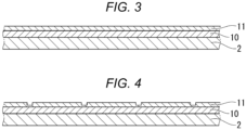
- FIG. 2 is a flowchart illustrating the method for manufacturing the piezoelectric substrate 100.
- FIGS. 3 to 5 are cross-sectional views schematically showing processes of manufacturing the piezoelectric substrate 100.
- the method for manufacturing the piezoelectric layer 20 is not limited to the wet method, and may be, for example, a gas phase method.
- a direction of the warpage of the piezoelectric substrate 100 may be upwardly convex. That is, in the solution method and the gas phase method, directions of the warpage of the piezoelectric substrate 100 may be different.
- other configurations are the same, and operations and effects thereof are also similar.
- the substrate 2 is prepared (substrate preparation step; step S1).
- a silicon oxide layer is formed by thermally oxidizing a silicon substrate.
- a zirconium layer is formed by a sputtering method or the like at the silicon oxide layer, and a zirconium oxide layer is formed by thermally oxidizing the zirconium layer.
- the substrate 2 can be prepared by the above steps.
- the first electrode 10 is formed at the substrate 2 (first film formation step; step S2).
- the first electrode 10 is formed by, for example, a sputtering method or a vacuum deposition method.
- the first electrode 10 is formed after a metal titanium film or the like is formed as the adhesion layer at the substrate 2.
- the adhesion layer can be formed by a sputtering method or the like.
- step S3 the seed layer 11 is formed at the first electrode 10 (second film formation step; step S3).
- the seed layer 11 is formed by, for example, a sputtering method, a vacuum deposition method, or a chemical solution method (wet method).
- examples of the material of the seed layer 11 include the compound containing bismuth, iron, titanium, and lead, lithium and niobium oxides (LiNbO), zinc oxide (ZnO), KNbO 3 , NaNbO 3 , LaNiOs, SrRuO 3 , SrTiOs, TiO, Zn, and Ti.
- the compound containing bismuth, iron, titanium, and lead is preferred.
- step S4 At least a part of the seed layer 11 is removed or modified.
- the seed layer 11 corresponding to the stress relaxation region R2 in the seed layer 11 is removed or modified. Accordingly, the orientation and the crystallinity of the piezoelectric layer 20 formed at the seed layer 11 are reduced. That is, since the region where the seed layer 11 is removed or modified is a region that does not function as a device, the region where the seed layer 11 is removed is the portion that substantially coincides with the line cut when the piezoelectric substrate 100 is divided into a desired device chip size, and the seed layer 11 in a region that functions as the device remains.
- FIG. 4 shows a case where a part of the seed layer 11 corresponding to the stress relaxation region R2 is removed such that a part of the seed layer 11 remains, but the embodiment is not limited thereto.
- the entire seed layer 11 corresponding to the stress relaxation region R2 may be removed, or the seed layer 11 may be modified by controlling a laser output to an extent that ablation does not occur.
- the seed layer 11 may be removed or modified by emitting a laser onto the seed layer 11.
- ablation processing using laser light may be adopted.
- Laser irradiation conditions are not particularly limited.
- a type of the laser light may be any type as long as the laser light can impart excessive thermal energy to a film, and may be pulse light or continuous light in a wavelength range from IR to UV.
- the stress relaxation region R2 can be formed in any shape without forming a resist mask or the like.
- the seed layer 11 may be removed by etching. Since the etching has a larger number of steps than the laser processing, the etching may be poor in productivity. However, since the etching is more excellent in mass productivity than the laser processing, the etching may be appropriately selected.
- the seed layer 11 may be removed by blasting. Similar to the etching, since the blasting has a large number of steps, the blasting may be poor in productivity. However, since the blasting is more excellent in mass productivity than the laser processing, and is more excellent in surface modification properties than the etching, the blasting may be appropriately selected.
- a processing width (a width of an irradiation trace in a case of the laser irradiation) when removing or modifying the seed layer 11 is not particularly limited.
- the stress relaxation region R2 is a region that does not function as a device, it is not preferable that the processing width is excessively large. Further, when the processing width is excessively small, the region may not sufficiently function as the region for reducing the orientation and the crystallinity of the piezoelectric layer 20. Therefore, the processing width when removing or modifying the seed layer 11 is preferably 1 ⁇ m to 100 ⁇ m.
- the piezoelectric layer 20 is formed (third film formation step; step S5).
- the piezoelectric layer 20 is obtained by, for example, forming a plurality of piezoelectric films.
- the piezoelectric layer 20 is formed of the plurality of piezoelectric films.
- the piezoelectric layer 20 can be formed by, for example, a chemical solution method (wet method) in which a solution containing a metal complex (precursor solution) is applied and dried, and further fired to obtain a metal oxide.
- the piezoelectric layer 20 can also be formed by a laser ablation method, a sputtering method, a pulsed laser deposition method (PLD method), a chemical vapor deposition (CVD) method, an aerosol deposition method, or the like.
- PLD method pulsed laser deposition method
- CVD chemical vapor deposition
- aerosol deposition method or the like.
- the wet method liquid phase method
- the wet method is a method for forming a film by a chemical solution method such as a MOD method or a sol-gel method, and is a concept distinguished from a gas phase method such as a sputtering method.
- the gas phase method may be used in addition to the wet method.
- the piezoelectric layer 20 formed by the wet method includes a plurality of piezoelectric films formed by a series of steps including a step of applying a precursor solution to form a precursor film (application step), a step of drying the precursor film (drying step), a step of heating and degreasing the dried precursor film (degreasing step), and a step of firing the degreased precursor film (firing step). That is, the piezoelectric layer 20 is formed by repeating the series of steps from the application step to the firing step a plurality of times. In the series of steps described above, the firing step may be performed after repeating steps from the application step to the degreasing step a plurality of times.
- a specific procedure when forming the piezoelectric layer 20 by the wet method is, for example, as follows.
- a precursor solution containing a predetermined metal complex is prepared.
- the precursor solution is a solution in which a metal complex that can form a composite oxide containing K, Na, and Nb by firing is dissolved or dispersed in an organic solvent.
- a metal complex containing an additive such as Mn, Li, or Cu may be further mixed.
- the metal complex containing Mn, Li, or Cu is mixed with the precursor solution, insulation properties of the obtained piezoelectric layer 20 can be further enhanced.
- Examples of a metal complex containing potassium (K) include potassium 2-ethylhexanoate and potassium acetate.
- Examples of a metal complex containing sodium (Na) include sodium 2-ethylhexanoate and sodium acetate.
- Examples of a metal complex containing niobium (Nb) include niobium 2-ethylhexanoate and pentaethoxyniobium.
- Mn is added as an additive
- examples of a metal complex containing Mn include manganese 2-ethylhexanoate.
- examples of a metal complex containing Li include lithium 2-ethylhexanoate. At this time, two or more kinds of metal complexes may be used in combination.
- the metal complex containing potassium (K) potassium 2-ethylhexanoate and potassium acetate may be used in combination.
- the solvent include 2-n-butoxyethanol, n-octane, or a mixed solvent thereof.
- the precursor solution may contain an additive for stabilizing dispersion of the metal complex containing K, Na, and Nb. Examples of such an additive include 2-ethylhexanoic acid.
- the precursor solution described above is applied at the seed layer 11 to form a precursor film (application step).
- the precursor film is heated to a predetermined temperature, for example, about 150°C to 300°C, and dried for a certain period of time (drying step).
- the dried precursor film is heated to a predetermined temperature, for example, 300°C to 500°C, and degreased by holding the precursor film at the temperature for a certain period of time (degreasing step).
- a predetermined temperature for example, 300°C to 500°C
- the degreased precursor film is heated to a high temperature, for example, about 500°C to 900°C, and crystallized by holding the precursor film at the temperature for a certain period of time (firing step). Accordingly, the piezoelectric film is completed.
- the heating temperature in the firing step is preferably high from a viewpoint of increasing the density of the piezoelectric layer 20 and improving the crystal directionality. Specifically, the heating temperature is preferably 700°C or higher. More preferably, the heating temperature is 750°C or higher. On the other hand, when the heating temperature in the firing step is excessively high, an alkali metal diffuses into the first electrode 10, and thus the composition of the piezoelectric layer 20 may change and the crystal directionality may deteriorate. Therefore, the heating temperature is preferably 850°C or lower.
- Examples of a heating device used in the drying step, the degreasing step, and the firing step include a rapid thermal annealing (RTA) device that performs heating by, for example, irradiation of an infrared lamp, and a hot plate.
- RTA rapid thermal annealing
- the piezoelectric layer 20 formed of the plurality of piezoelectric films is formed by repeating the steps described above a plurality of times.
- the number of repetitions of the series of steps is not particularly limited. Further, the piezoelectric layer 20 formed of one piezoelectric film may be formed without repeating the steps described above a plurality of times.
- the firing step may be performed after steps from the application step to the degreasing step are repeated a plurality of times.
- the piezoelectric layer 20 can be formed at the seed layer 11 by the steps described above.
- the piezoelectric layer 20 formed above the seed layer 11 becomes a low orientation region 20A where the crystallinity and the orientation deteriorate.
- the low orientation region 20A where the orientation and the crystallinity deteriorate is a region where there is a large amount of non-uniform and heterogeneous regions per unit area that can become a starting point of a crack, and the crack selectively and intentionally occurs in the region.
- a low orientation region 20A exists at substantially the same position and in substantially the same shape as a dividing line of the device, the stress is divided in the low orientation region 20A even when there is no change in stress in a region other than the low orientation region 20A, that is, the active portion region (first region) R1, and therefore a deformation amount of the entire piezoelectric substrate 100 can be reduced. As a result, the warpage amount can be reduced.
- the low orientation region 20A since it can be said that in the low orientation region 20A with many cracks, a Young's modulus when looking at the entire region on average is smaller than that in a region where there is no crack, the low orientation region 20A rather than the active portion region R1 (that is, the stress relaxation region R2) largely deforms by an external force during wafer handling. As a result, a crack in the active portion region R1 can be prevented.
- the second electrode (upper electrode) may be formed at the piezoelectric layer 20, and the piezoelectric layer 20 and the second electrode may be patterned.
- the second electrode may be formed by, for example, a sputtering method or a vacuum deposition method.
- the piezoelectric substrate 100 according to the first embodiment can be manufactured by the steps described above.
- the second film formation step is executed after the first film formation step.
- the first electrode 10 may be patterned between the first film formation step and the second film formation step. That is, in the piezoelectric substrate 100 according to the second embodiment, the first electrode 10 is provided as an individual electrode.
- the second electrode can be set as a common electrode. Accordingly, since the second electrode covers the piezoelectric layer 20, formation of a protection film that covers the piezoelectric layer 20 can be simplified.
- the piezoelectric substrate 100 can be suitably used for a liquid-discharging head and a printer, but is not limited thereto, and can be used in a wide range of applications.
- the piezoelectric substrate 100 is suitably used as, for example, a piezoelectric actuator such as an ultrasonic motor, a vibrating dust removal device, a piezoelectric transformer, a piezoelectric speaker, a piezoelectric pump, and a pressure-electricity converter.
- the piezoelectric substrate 100 is suitably used as, for example, a piezoelectric sensor element such as an ultrasonic detector, an angular velocity sensor, an acceleration sensor, a vibration sensor, an inclination sensor, a pressure sensor, a collision sensor, a human sensor, an infrared sensor, a terahertz sensor, a thermal detection sensor, a pyroelectric sensor, and a piezoelectric sensor.
- the piezoelectric substrate 100 is suitably used as a ferroelectric element such as a ferroelectric memory (FeRAM), a ferroelectric transistor (FeFET), a ferroelectric calculation circuit (FeLogic), and a ferroelectric capacitor.
- the piezoelectric substrate 100 is suitably used as a voltage-control optical element such as a wavelength converter, an optical waveguide, an optical path modulator, a refractive index control element, and an electronic shutter mechanism.
Landscapes
- Engineering & Computer Science (AREA)
- Chemical & Material Sciences (AREA)
- Manufacturing & Machinery (AREA)
- Materials Engineering (AREA)
- Ceramic Engineering (AREA)
- Dispersion Chemistry (AREA)
- Particle Formation And Scattering Control In Inkjet Printers (AREA)
Abstract
Description
- The present application is based on, and claims priority from
JP Application Serial Number 2023-037305, filed March 10, 2023 - The present disclosure relates to a method for manufacturing a piezoelectric substrate and a piezoelectric substrate.
- Generally, a piezoelectric substrate includes a substrate, a piezoelectric layer having electromechanical conversion characteristics, and two electrode layers that sandwich the piezoelectric layer. In recent years, devices using such a piezoelectric substrate as a driving source (piezoelectric element application devices) have been actively developed. As one of the piezoelectric element application devices, a liquid ejecting head represented by an ink jet type recording head, a MEMS element represented by a piezoelectric MEMS element, an ultrasonic measurement device represented by an ultrasonic sensor or the like, and a piezoelectric actuator device or the like are provided.
- As a material (piezoelectric material) of the piezoelectric layer of the piezoelectric substrate, lead zirconate titanate (PZT) is known. However, in recent years, from a viewpoint of reducing an environmental load, progress has been made in development of a lead-free piezoelectric material with a reduced content of lead.
-
JP-A-2011-29591 -
JP-A-2011-29591 - The piezoelectric substrate is manufactured by laminating the substrate, the electrode layers, and the piezoelectric layer made of different materials. Therefore, when a temperature change occurs because of a heat treatment or the like, since thermal expansion coefficients of the materials are different, there is a problem that the entire piezoelectric substrate is warped due to a thermal stress. Further, when a warpage amount increases, a problem such as a crack occurring in the piezoelectric substrate, particularly in the piezoelectric layer, or interlayer delamination occurring between the substrate and the piezoelectric layer may occur.
- In order to solve such a problem,
JP-A-2011-29591 - Under these circumstances, there is a need for a piezoelectric substrate that can reduce the warpage amount of the entire substrate due to the thermal stress.
- Such a problem is not limited to existing in a piezoelectric substrate used in a piezoelectric actuator mounted on a liquid ejecting head represented by an ink jet type recording head, and also exists in a piezoelectric substrate used in other piezoelectric element application devices.
- In order to solve the problems described above, a first aspect of the present disclosure provides a method for manufacturing a piezoelectric substrate, the method including: a first film formation step of forming a first electrode at a substrate; a second film formation step of forming a seed layer at the first electrode; a processing step of removing or modifying at least a part of the seed layer; and a third film formation step of forming a piezoelectric layer containing potassium, sodium, and niobium at the seed layer and the first electrode, in which the substrate includes a stress relaxation region, and in the processing step, the seed layer corresponding to the stress relaxation region is removed or modified.
-
-
FIG. 1 is a cross-sectional view schematically showing a piezoelectric substrate according to a first embodiment. -
FIG. 2 is a flowchart illustrating a method for manufacturing the piezoelectric substrate according to the first embodiment. -
FIG. 3 is a cross-sectional view schematically showing a process of manufacturing the piezoelectric substrate according to the first embodiment. -
FIG. 4 is a cross-sectional view schematically showing a process of manufacturing the piezoelectric substrate according to the first embodiment. -
FIG. 5 is a cross-sectional view schematically showing a process of manufacturing the piezoelectric substrate according to the first embodiment. - Hereinafter, embodiments of the present disclosure will be described with reference to the drawings. The following description shows an aspect of the present disclosure, and can be optionally changed within a range not departing from the gist of the present disclosure. In the drawings, the same reference signs denote the same members, and description thereof will be appropriately omitted. The numeral after the characters forming the reference signs are referred to with reference signs including the same characters, and used for distinguishing elements having similar structures from each other. When it is not necessary to distinguish elements indicated by reference signs including the same characters from each other, the elements will be referred to with reference signs including only characters.
- In the drawings, X, Y, and Z represent three spatial axes orthogonal to one another. In the present specification, directions along the axes are a first direction X (X direction), a second direction Y (Y direction), and a third direction Z (Z direction), respectively. A direction facing an arrow in each drawing is described as a positive (+) direction, and a direction opposite to the arrow is described as a negative (-) direction. The X direction and the Y direction represent an in-plane direction of a plate, a layer, and a film, and the Z direction represents a thickness direction or a lamination direction of the plate, the layer, and the film.
- Elements shown in the drawings, that is, a shape or a size of each part, thicknesses of a plate, a layer, and a film, a relative positional relationship, a repeated unit, and the like may be exaggeratedly shown for the purpose of describing the present disclosure. Further, the term "at" in the present specification does not limit a positional relationship of elements to "directly above". For example, expressions such as "a first electrode at a substrate" and "a piezoelectric layer at the first electrode" to be described later do not exclude a fact that another element is provided between the substrate and the first electrode or between the first electrode and the piezoelectric layer.
- First, a piezoelectric substrate and a method for manufacturing the piezoelectric substrate according to the first embodiment will be described with reference to the drawings.
-
FIG. 1 is a cross-sectional view schematically showing apiezoelectric substrate 100 according to the embodiment. - As shown in
FIG. 1 , thepiezoelectric substrate 100 includes asubstrate 2, a first electrode (lower electrode) 10, aseed layer 11, and apiezoelectric layer 20. - The
substrate 2 is a flat plate formed of, for example, a semiconductor or an insulator. Thesubstrate 2 may be a single layer, or a laminate where a plurality of layers are laminated. An internal structure of thesubstrate 2 is not limited as long as an upper surface has a planar shape, and thesubstrate 2 may have a structure in which a space or the like is formed therein. - The
substrate 2 may include a vibration plate that has flexibility and that deforms by an operation of thepiezoelectric layer 20. The vibration plate is, for example, a silicon oxide layer, a titanium oxide layer, a zirconium oxide layer, a laminate where the zirconium oxide layer is provided at the silicon oxide layer, or a laminate where the titanium oxide layer and the zirconium oxide layer are provided at the silicon oxide layer. - The
substrate 2 includes active portion regions (first regions) R1 that are regions functioning as devices, and stress relaxation regions (second regions) R2 that are regions other than the active portion regions R1. The stress relaxation region R2 is a region for reducing orientation and crystallinity of thepiezoelectric layer 20, and is a region that does not function as a device. That is, the stress relaxation region R2 is provided at a portion that substantially coincides with a line cut when thepiezoelectric substrate 100 is divided into a desired device chip size. The stress relaxation region R2 corresponds to a region where a part of theseed layer 11 is removed or modified, which will be described later. - The
first electrode 10 is provided at thesubstrate 2. Thefirst electrode 10 is provided between thesubstrate 2 and thepiezoelectric layer 20. A shape of thefirst electrode 10 is, for example, a layer. A thickness of thefirst electrode 10 is, for example, 20 nm or more and 200 nm or less. Thefirst electrode 10 is, for example, a metal layer such as a platinum layer, an iridium layer, or a ruthenium layer, a conductive oxide layer thereof, a lanthanum nickelate (LaNiO3: LNO) layer, or a strontium ruthenate (SrRuO3: SRO) layer. Thefirst electrode 10 may have a structure in which a plurality of layers exemplified above are laminated. - An adhesion layer (not shown) such as a titanium layer may be provided between the
substrate 2 and thefirst electrode 10. The adhesion layer is formed of, for example, a titanium oxide (TiOx), titanium (Ti), or SiN, and has a function of improving adhesiveness between thepiezoelectric layer 20 and thesubstrate 2. Further, when the titanium oxide (TiOx) layer, the titanium (Ti) layer, or a silicon nitride (SiN) layer is used as the adhesion layer, the adhesion layer also has a function serving as a stopper to prevent constituent elements of the piezoelectric layer 20 (for example, potassium and sodium) from passing through thefirst electrode 10 and reaching thesubstrate 2 when forming thepiezoelectric layer 20 to be described later. The adhesion layer may be omitted. - The
first electrode 10 is one electrode for applying a voltage to thepiezoelectric layer 20. Thefirst electrode 10 is a lower electrode provided below thepiezoelectric layer 20. Thefirst electrode 10 may be an individual electrode or a common electrode. - The seed layer (orientation control layer) 11 is provided at the
first electrode 10, and has a function of controlling orientation of crystals of a piezoelectric body constituting thepiezoelectric layer 20. That is, by providing theseed layer 11 at thefirst electrode 10, the crystals of the piezoelectric body constituting thepiezoelectric layer 20 can be preferentially oriented in a predetermined plane orientation (for example, (100) plane). When the crystal orientation of thepiezoelectric layer 20 is improved, it is possible to efficiently use domain rotation and improve displacement characteristics of thepiezoelectric layer 20. - At least a part of the
seed layer 11 is removed or modified. Specifically, at least a part of theseed layer 11 at a position corresponding to the stress relaxation region R2 is removed or modified by laser irradiation or the like. Therefore, a thermal mark may be formed as a trace of theseed layer 11 at a position corresponding to the stress relaxation region R2. When removing theseed layer 11 at the position corresponding to the stress relaxation region R2, theentire seed layer 11 may be removed in a thickness direction or theseed layer 11 may be removed such that a part thereof remains. Further, by adjusting removal conditions (for example, laser irradiation conditions), theseed layer 11 can be modified without being removed. Crystal grains of thepiezoelectric layer 20 formed at any location where theseed layer 11 is removed or modified are not preferentially oriented in a predetermined plane orientation by the seed layer. Therefore, a crack can occur in the stress relaxation region R2, and warpage of the entirepiezoelectric substrate 100 can be reduced. - A surface roughness of the
piezoelectric layer 20 in the stress relaxation region R2 may be larger than a surface roughness of thepiezoelectric layer 20 in the active portion region R1. As described above, since the crystal grains of thepiezoelectric layer 20 formed at the portion where theseed layer 11 is removed or modified are not preferentially oriented in a predetermined plane orientation by the seed layer, the surface roughness of thepiezoelectric layer 20 in the stress relaxation region R2 is large. - A thickness of the
seed layer 11 is, for example, 1 nm or more and 20 nm or less. The thickness of theseed layer 11 referred here is a thickness of a portion not removed or modified for forming the stress relaxation region R2. - Examples of a material of the
seed layer 11 include a compound containing bismuth, iron, titanium, and lead, lithium and niobium oxides (LiNbO), zinc oxide (ZnO), KNbO3, NaNbO3, LaNiOs, SrRuO3, SrTiO3, TiO, Zn, and Ti. Among them, the compound containing bismuth, iron, titanium, and lead is preferred. When the compound containing bismuth, iron, titanium, and lead is used as the material of theseed layer 11, the crystal structure of the KNN-basedpiezoelectric layer 20 can be further stabilized. That is, when thepiezoelectric layer 20 is formed using the compound containing bismuth, iron, titanium, and lead as theseed layer 11, stability of potassium and sodium in thepiezoelectric layer 20 can be improved. As a result, diffusion of potassium and sodium toward asubstrate 2 side can be further prevented. - The
piezoelectric layer 20 is provided at thefirst electrode 10, and is formed in the active portion region R1 and the stress relaxation region R2 above thesubstrate 2. A thickness of thepiezoelectric layer 20 is, for example, 100 nm or more and 3000 nm or less. Thepiezoelectric layer 20 can deform by applying a voltage between thefirst electrode 10 and a second electrode (not shown) that is an upper electrode. - The
piezoelectric layer 20 is preferably a composite oxide having a perovskite structure represented by a general formula ABO3, and more preferably contains a piezoelectric material represented by the following formula (1) and formed of potassium sodium niobate (KNN-based composite oxide; (K, Na)NbOs).
(KX, Na1-X)NbO3... (1)

- The composite oxide represented by above formula (1) is a so-called KNN-based composite oxide. The KNN-based composite oxide is a lead-free piezoelectric material with a reduced content of lead (Pb) or the like, and therefore has excellent biocompatibility and a small environmental load. Further, the KNN-based composite oxide is excellent in piezoelectric characteristics among a lead-free piezoelectric material, and is therefore advantageous in improving various characteristics.
- The
piezoelectric layer 20 may contain an additive other than elements (for example, niobium, potassium, sodium, and oxygen) constituting the composite oxide having a perovskite structure described above. That is, thepiezoelectric layer 20 may be, for example, a KNN layer to which an additive is added. Examples of such an additive include manganese (Mn). - The
piezoelectric layer 20 does not contain, for example, lead (Pb). Thepiezoelectric layer 20 being free of lead can be confirmed by, for example, X-Ray fluorescence (XRF) measurement. - The upper electrode (second electrode) is provided at the
piezoelectric layer 20. The second electrode may be further provided at a side surface of thepiezoelectric layer 20 and at thesubstrate 2 as long as the second electrode is electrically separated from thefirst electrode 10. - A shape of the second electrode is, for example, a layer. The second electrode is, for example, a metal layer such as an iridium layer, a platinum layer, or a ruthenium layer, a conductive oxide layer thereof, a lanthanum nickelate layer, or a strontium ruthenate layer. The second electrode may have a structure in which a plurality of layers exemplified above are laminated. The material of the
first electrode 10 and the material of the second electrode may be the same as or different from each other. - The second electrode is another electrode for applying a voltage to the
piezoelectric layer 20. The second electrode functions as the upper electrode provided at thepiezoelectric layer 20. - As shown in
FIG. 1 , in thepiezoelectric substrate 100 according to the embodiment, a plurality of first regions R1 and a plurality of second regions R2 have a downwardly convex shape. That is, it can be said that when thepiezoelectric substrate 100 is viewed in a cross section, both the first regions R1 and the second regions R2 are curved toward thesubstrate 2 side, and thesubstrate 2 has a plurality of centers of curvature. - States of warpage of the first region R1 and the second region R2 may be different from each other. For example, a curvature radius of the first region R1 is smaller than a curvature radius of the second region R2. In this way, when the first region R1 and the second region R2 have curvatures instead of providing one curvature over the entire
piezoelectric substrate 100, a residual stress of thepiezoelectric layer 20 can be relaxed, and a warpage amount of the entirepiezoelectric substrate 100 can be reduced. - As described above, the second region R2 that is the stress relaxation region corresponds to the region where a part of the
seed layer 11 is removed or modified. That is, the second region R2 is a region for intentionally reducing the crystal orientation. In thepiezoelectric layer 20 corresponding to the second region R2, the orientation and the crystallinity naturally deteriorate. Crystal grains not on a preferentially oriented plane by the seed layer increase in size. When the orientation and the crystallinity of thepiezoelectric layer 20 deteriorate, a crack is more likely to occur preferentially in thepiezoelectric layer 20 than in the first region R1 that is the active portion region. As a result, even when a thermal stress is applied to the entirepiezoelectric substrate 100, the stress can be relaxed in the second region R2 and the warpage amount of the entirepiezoelectric substrate 100 can be reduced. - Next, a method for manufacturing the
piezoelectric substrate 100 will be described with reference to the drawings.FIG. 2 is a flowchart illustrating the method for manufacturing thepiezoelectric substrate 100.FIGS. 3 to 5 are cross-sectional views schematically showing processes of manufacturing thepiezoelectric substrate 100. In the following description, a case where thepiezoelectric layer 20 is manufactured by a chemical solution method (wet method) will be described. However, the method for manufacturing thepiezoelectric layer 20 is not limited to the wet method, and may be, for example, a gas phase method. When thepiezoelectric layer 20 is formed by the gas phase method, a direction of the warpage of thepiezoelectric substrate 100 may be upwardly convex. That is, in the solution method and the gas phase method, directions of the warpage of thepiezoelectric substrate 100 may be different. However, other configurations are the same, and operations and effects thereof are also similar. - As shown in
FIG. 3 , thesubstrate 2 is prepared (substrate preparation step; step S1). - Specifically, for example, a silicon oxide layer is formed by thermally oxidizing a silicon substrate. Next, a zirconium layer is formed by a sputtering method or the like at the silicon oxide layer, and a zirconium oxide layer is formed by thermally oxidizing the zirconium layer. The
substrate 2 can be prepared by the above steps. - Next, the
first electrode 10 is formed at the substrate 2 (first film formation step; step S2). - The
first electrode 10 is formed by, for example, a sputtering method or a vacuum deposition method. When an adhesion layer is provided, thefirst electrode 10 is formed after a metal titanium film or the like is formed as the adhesion layer at thesubstrate 2. The adhesion layer can be formed by a sputtering method or the like. - Next, the
seed layer 11 is formed at the first electrode 10 (second film formation step; step S3). - The
seed layer 11 is formed by, for example, a sputtering method, a vacuum deposition method, or a chemical solution method (wet method). As described above, examples of the material of theseed layer 11 include the compound containing bismuth, iron, titanium, and lead, lithium and niobium oxides (LiNbO), zinc oxide (ZnO), KNbO3, NaNbO3, LaNiOs, SrRuO3, SrTiOs, TiO, Zn, and Ti. Among them, the compound containing bismuth, iron, titanium, and lead is preferred. - Next, as shown in
FIG. 4 , at least a part of theseed layer 11 is removed or modified (processing step; step S4). - The
seed layer 11 corresponding to the stress relaxation region R2 in theseed layer 11 is removed or modified. Accordingly, the orientation and the crystallinity of thepiezoelectric layer 20 formed at theseed layer 11 are reduced. That is, since the region where theseed layer 11 is removed or modified is a region that does not function as a device, the region where theseed layer 11 is removed is the portion that substantially coincides with the line cut when thepiezoelectric substrate 100 is divided into a desired device chip size, and theseed layer 11 in a region that functions as the device remains.FIG. 4 shows a case where a part of theseed layer 11 corresponding to the stress relaxation region R2 is removed such that a part of theseed layer 11 remains, but the embodiment is not limited thereto. Theentire seed layer 11 corresponding to the stress relaxation region R2 may be removed, or theseed layer 11 may be modified by controlling a laser output to an extent that ablation does not occur. - The
seed layer 11 may be removed or modified by emitting a laser onto theseed layer 11. Specifically, ablation processing using laser light may be adopted. Laser irradiation conditions are not particularly limited. When performing the ablation processing using the laser light, a type of the laser light may be any type as long as the laser light can impart excessive thermal energy to a film, and may be pulse light or continuous light in a wavelength range from IR to UV. When performing the processing step by the laser irradiation, the stress relaxation region R2 can be formed in any shape without forming a resist mask or the like. - The
seed layer 11 may be removed by etching. Since the etching has a larger number of steps than the laser processing, the etching may be poor in productivity. However, since the etching is more excellent in mass productivity than the laser processing, the etching may be appropriately selected. - The
seed layer 11 may be removed by blasting. Similar to the etching, since the blasting has a large number of steps, the blasting may be poor in productivity. However, since the blasting is more excellent in mass productivity than the laser processing, and is more excellent in surface modification properties than the etching, the blasting may be appropriately selected. - A processing width (a width of an irradiation trace in a case of the laser irradiation) when removing or modifying the
seed layer 11 is not particularly limited. However, when it is considered that the stress relaxation region R2 is a region that does not function as a device, it is not preferable that the processing width is excessively large. Further, when the processing width is excessively small, the region may not sufficiently function as the region for reducing the orientation and the crystallinity of thepiezoelectric layer 20. Therefore, the processing width when removing or modifying theseed layer 11 is preferably 1 µm to 100 µm. - Next, as shown in
FIG. 5 , thepiezoelectric layer 20 is formed (third film formation step; step S5). Thepiezoelectric layer 20 is obtained by, for example, forming a plurality of piezoelectric films. Thepiezoelectric layer 20 is formed of the plurality of piezoelectric films. Thepiezoelectric layer 20 can be formed by, for example, a chemical solution method (wet method) in which a solution containing a metal complex (precursor solution) is applied and dried, and further fired to obtain a metal oxide. In addition, thepiezoelectric layer 20 can also be formed by a laser ablation method, a sputtering method, a pulsed laser deposition method (PLD method), a chemical vapor deposition (CVD) method, an aerosol deposition method, or the like. In the embodiment, from a viewpoint of improving the crystal orientation of thepiezoelectric layer 20, it is preferable to use the wet method (liquid phase method). - Here, the wet method is a method for forming a film by a chemical solution method such as a MOD method or a sol-gel method, and is a concept distinguished from a gas phase method such as a sputtering method. In the embodiment, the gas phase method may be used in addition to the wet method.
- For example, the
piezoelectric layer 20 formed by the wet method (liquid phase method) includes a plurality of piezoelectric films formed by a series of steps including a step of applying a precursor solution to form a precursor film (application step), a step of drying the precursor film (drying step), a step of heating and degreasing the dried precursor film (degreasing step), and a step of firing the degreased precursor film (firing step). That is, thepiezoelectric layer 20 is formed by repeating the series of steps from the application step to the firing step a plurality of times. In the series of steps described above, the firing step may be performed after repeating steps from the application step to the degreasing step a plurality of times. - A specific procedure when forming the
piezoelectric layer 20 by the wet method (liquid phase method) is, for example, as follows. - First, a precursor solution containing a predetermined metal complex is prepared. The precursor solution is a solution in which a metal complex that can form a composite oxide containing K, Na, and Nb by firing is dissolved or dispersed in an organic solvent. At this time, a metal complex containing an additive such as Mn, Li, or Cu may be further mixed. When the metal complex containing Mn, Li, or Cu is mixed with the precursor solution, insulation properties of the obtained
piezoelectric layer 20 can be further enhanced. - Examples of a metal complex containing potassium (K) include potassium 2-ethylhexanoate and potassium acetate. Examples of a metal complex containing sodium (Na) include sodium 2-ethylhexanoate and sodium acetate. Examples of a metal complex containing niobium (Nb) include niobium 2-ethylhexanoate and pentaethoxyniobium. When Mn is added as an additive, examples of a metal complex containing Mn include manganese 2-ethylhexanoate. When Li is added as an additive, examples of a metal complex containing Li include lithium 2-ethylhexanoate. At this time, two or more kinds of metal complexes may be used in combination. For example, as the metal complex containing potassium (K), potassium 2-ethylhexanoate and potassium acetate may be used in combination. Examples of the solvent include 2-n-butoxyethanol, n-octane, or a mixed solvent thereof. The precursor solution may contain an additive for stabilizing dispersion of the metal complex containing K, Na, and Nb. Examples of such an additive include 2-ethylhexanoic acid.
- Then, as shown in
FIG. 5 , the precursor solution described above is applied at theseed layer 11 to form a precursor film (application step). - Next, the precursor film is heated to a predetermined temperature, for example, about 150°C to 300°C, and dried for a certain period of time (drying step).
- Next, the dried precursor film is heated to a predetermined temperature, for example, 300°C to 500°C, and degreased by holding the precursor film at the temperature for a certain period of time (degreasing step).
- Finally, the degreased precursor film is heated to a high temperature, for example, about 500°C to 900°C, and crystallized by holding the precursor film at the temperature for a certain period of time (firing step). Accordingly, the piezoelectric film is completed.
- The heating temperature in the firing step is preferably high from a viewpoint of increasing the density of the
piezoelectric layer 20 and improving the crystal directionality. Specifically, the heating temperature is preferably 700°C or higher. More preferably, the heating temperature is 750°C or higher. On the other hand, when the heating temperature in the firing step is excessively high, an alkali metal diffuses into thefirst electrode 10, and thus the composition of thepiezoelectric layer 20 may change and the crystal directionality may deteriorate. Therefore, the heating temperature is preferably 850°C or lower. - Examples of a heating device used in the drying step, the degreasing step, and the firing step include a rapid thermal annealing (RTA) device that performs heating by, for example, irradiation of an infrared lamp, and a hot plate. The
piezoelectric layer 20 formed of the plurality of piezoelectric films is formed by repeating the steps described above a plurality of times. - The number of repetitions of the series of steps is not particularly limited. Further, the
piezoelectric layer 20 formed of one piezoelectric film may be formed without repeating the steps described above a plurality of times. - In the series of steps from the application step to the firing step, the firing step may be performed after steps from the application step to the degreasing step are repeated a plurality of times.
- As shown in
FIG. 5 , thepiezoelectric layer 20 can be formed at theseed layer 11 by the steps described above. In the manufacturing method according to the embodiment, since a part of theseed layer 11 corresponding to the stress relaxation region R2 is removed or modified, thepiezoelectric layer 20 formed above theseed layer 11 becomes alow orientation region 20A where the crystallinity and the orientation deteriorate. - The
low orientation region 20A where the orientation and the crystallinity deteriorate is a region where there is a large amount of non-uniform and heterogeneous regions per unit area that can become a starting point of a crack, and the crack selectively and intentionally occurs in the region. When such alow orientation region 20A exists at substantially the same position and in substantially the same shape as a dividing line of the device, the stress is divided in thelow orientation region 20A even when there is no change in stress in a region other than thelow orientation region 20A, that is, the active portion region (first region) R1, and therefore a deformation amount of the entirepiezoelectric substrate 100 can be reduced. As a result, the warpage amount can be reduced. Further, since it can be said that in thelow orientation region 20A with many cracks, a Young's modulus when looking at the entire region on average is smaller than that in a region where there is no crack, thelow orientation region 20A rather than the active portion region R1 (that is, the stress relaxation region R2) largely deforms by an external force during wafer handling. As a result, a crack in the active portion region R1 can be prevented. - The subsequent steps may be appropriately performed when necessary. For example, the second electrode (upper electrode) may be formed at the
piezoelectric layer 20, and thepiezoelectric layer 20 and the second electrode may be patterned. The second electrode may be formed by, for example, a sputtering method or a vacuum deposition method. - The
piezoelectric substrate 100 according to the first embodiment can be manufactured by the steps described above. - In the
piezoelectric substrate 100 according to the first embodiment, the second film formation step is executed after the first film formation step. However, as a second embodiment, thefirst electrode 10 may be patterned between the first film formation step and the second film formation step. That is, in thepiezoelectric substrate 100 according to the second embodiment, thefirst electrode 10 is provided as an individual electrode. When thefirst electrode 10 is an individual electrode, the second electrode can be set as a common electrode. Accordingly, since the second electrode covers thepiezoelectric layer 20, formation of a protection film that covers thepiezoelectric layer 20 can be simplified. - The
piezoelectric substrate 100 according to the embodiment can be suitably used for a liquid-discharging head and a printer, but is not limited thereto, and can be used in a wide range of applications. Thepiezoelectric substrate 100 is suitably used as, for example, a piezoelectric actuator such as an ultrasonic motor, a vibrating dust removal device, a piezoelectric transformer, a piezoelectric speaker, a piezoelectric pump, and a pressure-electricity converter. Further, thepiezoelectric substrate 100 is suitably used as, for example, a piezoelectric sensor element such as an ultrasonic detector, an angular velocity sensor, an acceleration sensor, a vibration sensor, an inclination sensor, a pressure sensor, a collision sensor, a human sensor, an infrared sensor, a terahertz sensor, a thermal detection sensor, a pyroelectric sensor, and a piezoelectric sensor. Further, thepiezoelectric substrate 100 is suitably used as a ferroelectric element such as a ferroelectric memory (FeRAM), a ferroelectric transistor (FeFET), a ferroelectric calculation circuit (FeLogic), and a ferroelectric capacitor. Further, thepiezoelectric substrate 100 is suitably used as a voltage-control optical element such as a wavelength converter, an optical waveguide, an optical path modulator, a refractive index control element, and an electronic shutter mechanism.
Claims (7)
- A method for manufacturing a piezoelectric substrate, the method comprising:a first film formation step of forming a first electrode at a substrate;a second film formation step of forming a seed layer at the first electrode;a processing step of removing or modifying at least a part of the seed layer; anda third film formation step of forming a piezoelectric layer containing potassium, sodium, and niobium at the seed layer and the first electrode, whereinthe substrate includes a stress relaxation region, andin the processing step, the seed layer corresponding to the stress relaxation region is removed or modified.
- The method for manufacturing a piezoelectric substrate according to claim 1, wherein
in the processing step, the seed layer is removed or modified by emitting a laser onto the seed layer. - The method for manufacturing a piezoelectric substrate according to claim 1, wherein
in the processing step, the seed layer is removed by etching. - A piezoelectric substrate comprising:a substrate including a first region and a second region;a first electrode layer formed above the substrate;a seed layer formed in the first region above the substrate; anda piezoelectric layer formed in the first region and the second region above the substrate and containing potassium, sodium, and niobium, whereinthe substrate includes a plurality of centers of curvature.
- The piezoelectric substrate according to claim 4, whereinthe seed layer contains bismuth, iron, titanium, and lead, anda thickness of the seed layer is smaller than a thickness of the piezoelectric layer.
- The piezoelectric substrate according to claim 4, wherein
a surface roughness of the piezoelectric layer in the second region is larger than a surface roughness of the piezoelectric layer in the first region. - The piezoelectric substrate according to claim 4, wherein
a thermal mark is formed in the substrate in the second region.
Applications Claiming Priority (1)
| Application Number | Priority Date | Filing Date | Title |
|---|---|---|---|
| JP2023037305A JP2024128363A (en) | 2023-03-10 | 2023-03-10 | Piezoelectric substrate manufacturing method and piezoelectric substrate |
Publications (2)
| Publication Number | Publication Date |
|---|---|
| EP4429446A1 true EP4429446A1 (en) | 2024-09-11 |
| EP4429446B1 EP4429446B1 (en) | 2025-09-03 |
Family
ID=90236227
Family Applications (1)
| Application Number | Title | Priority Date | Filing Date |
|---|---|---|---|
| EP24162232.3A Active EP4429446B1 (en) | 2023-03-10 | 2024-03-08 | Method for manufacturing piezoelectric substrate and piezoelectric substrate |
Country Status (4)
| Country | Link |
|---|---|
| US (1) | US20240306509A1 (en) |
| EP (1) | EP4429446B1 (en) |
| JP (1) | JP2024128363A (en) |
| CN (1) | CN118632610A (en) |
Citations (5)
| Publication number | Priority date | Publication date | Assignee | Title |
|---|---|---|---|---|
| JP2011029591A (en) | 2009-06-22 | 2011-02-10 | Hitachi Cable Ltd | Piezoelectric thin film element and manufacturing method of piezoelectric thin film element, and piezoelectric thin film device |
| US8084925B2 (en) * | 2008-06-05 | 2011-12-27 | Hitachi Cable, Ltd. | Piezoelectric thin film elemental device, sensor and actuator |
| US20140132676A1 (en) * | 2012-11-12 | 2014-05-15 | Seiko Epson Corporation | Liquid ejecting head and liquid ejecting apparatus and actuator |
| US20160284969A1 (en) * | 2015-03-27 | 2016-09-29 | Seiko Epson Corporation | Piezoelectric element, piezoelectric element application device, and method of manufacturing piezoelectric element |
| JP2023037305A (en) | 2021-09-03 | 2023-03-15 | サトーホールディングス株式会社 | Rfid medium and rfid medium continuum |
-
2023
- 2023-03-10 JP JP2023037305A patent/JP2024128363A/en active Pending
-
2024
- 2024-03-06 CN CN202410254181.4A patent/CN118632610A/en active Pending
- 2024-03-08 US US18/599,762 patent/US20240306509A1/en active Pending
- 2024-03-08 EP EP24162232.3A patent/EP4429446B1/en active Active
Patent Citations (6)
| Publication number | Priority date | Publication date | Assignee | Title |
|---|---|---|---|---|
| US8084925B2 (en) * | 2008-06-05 | 2011-12-27 | Hitachi Cable, Ltd. | Piezoelectric thin film elemental device, sensor and actuator |
| JP2011029591A (en) | 2009-06-22 | 2011-02-10 | Hitachi Cable Ltd | Piezoelectric thin film element and manufacturing method of piezoelectric thin film element, and piezoelectric thin film device |
| US8304966B2 (en) * | 2009-06-22 | 2012-11-06 | Hitachi Cable, Ltd. | Piezoelectric thin film element and manufacturing method of the piezoelectric thin film element, piezoelectric thin film device |
| US20140132676A1 (en) * | 2012-11-12 | 2014-05-15 | Seiko Epson Corporation | Liquid ejecting head and liquid ejecting apparatus and actuator |
| US20160284969A1 (en) * | 2015-03-27 | 2016-09-29 | Seiko Epson Corporation | Piezoelectric element, piezoelectric element application device, and method of manufacturing piezoelectric element |
| JP2023037305A (en) | 2021-09-03 | 2023-03-15 | サトーホールディングス株式会社 | Rfid medium and rfid medium continuum |
Also Published As
| Publication number | Publication date |
|---|---|
| JP2024128363A (en) | 2024-09-24 |
| EP4429446B1 (en) | 2025-09-03 |
| US20240306509A1 (en) | 2024-09-12 |
| CN118632610A (en) | 2024-09-10 |
Similar Documents
| Publication | Publication Date | Title |
|---|---|---|
| US10297742B2 (en) | Piezoelectric element and device including the same | |
| CN104851970B (en) | The manufacture method of piezo-activator, jet head liquid and piezo-activator | |
| TWI253392B (en) | Dielectric member, piezoelectric member, ink jet head, ink jet recording apparatus and producing method for ink jet recording apparatus | |
| JP6922326B2 (en) | Piezoelectric element and piezoelectric element application device | |
| EP3002126B1 (en) | Liquid ejecting head, liquid ejecting apparatus, and piezoelectric device | |
| CN106486595B (en) | Piezoelectric Elements and Piezoelectric Element Application Equipment | |
| CN105529394B (en) | Piezoelectric element, manufacturing method thereof, and application device of piezoelectric element | |
| JP6805801B2 (en) | Piezoelectric elements and piezoelectric element application devices | |
| JP6610856B2 (en) | Piezoelectric element, piezoelectric element applied device, and method of manufacturing piezoelectric element | |
| CN108068458B (en) | Piezoelectric element and piezoelectric element application device | |
| CN103802478A (en) | Liquid ejecting head and liquid ejecting apparatus and actuator | |
| US20230371385A1 (en) | Piezoelectric Element And Liquid Droplet Dispensing Head | |
| JP6652736B2 (en) | Piezoelectric element and piezoelectric element application device | |
| JP2012169467A (en) | Composition for forming piezoelectric ceramics film, method for manufacturing piezoelectric element, and method for manufacturing liquid injection head | |
| EP4429446B1 (en) | Method for manufacturing piezoelectric substrate and piezoelectric substrate | |
| US20230354709A1 (en) | Method Of Manufacturing Piezoelectric Element | |
| CN120396523A (en) | Piezoelectric element, liquid ejection head, and printer | |
| US20230301192A1 (en) | Piezoelectric element | |
| EP2515357B1 (en) | Liquid ejecting head, liquid ejecting apparatus, and piezoelectric element | |
| JP2024128362A (en) | Manufacturing method of piezoelectric substrate | |
| JP6932966B2 (en) | Piezoelectric element and piezoelectric element application device | |
| US20240306511A1 (en) | Piezoelectric Element Application Device | |
| US11865838B2 (en) | Piezoelectric device, liquid ejecting head, liquid ejecting apparatus, and method of manufacturing piezoelectric device | |
| CN120206969A (en) | Piezoelectric element, liquid ejection head and printer | |
| CN120552485A (en) | Piezoelectric element, liquid ejection head, and printer |
Legal Events
| Date | Code | Title | Description |
|---|---|---|---|
| PUAI | Public reference made under article 153(3) epc to a published international application that has entered the european phase |
Free format text: ORIGINAL CODE: 0009012 |
|
| STAA | Information on the status of an ep patent application or granted ep patent |
Free format text: STATUS: THE APPLICATION HAS BEEN PUBLISHED |
|
| AK | Designated contracting states |
Kind code of ref document: A1 Designated state(s): AL AT BE BG CH CY CZ DE DK EE ES FI FR GB GR HR HU IE IS IT LI LT LU LV MC ME MK MT NL NO PL PT RO RS SE SI SK SM TR |
|
| STAA | Information on the status of an ep patent application or granted ep patent |
Free format text: STATUS: REQUEST FOR EXAMINATION WAS MADE |
|
| 17P | Request for examination filed |
Effective date: 20241018 |
|
| RBV | Designated contracting states (corrected) |
Designated state(s): AL AT BE BG CH CY CZ DE DK EE ES FI FR GB GR HR HU IE IS IT LI LT LU LV MC ME MK MT NL NO PL PT RO RS SE SI SK SM TR |
|
| RIC1 | Information provided on ipc code assigned before grant |
Ipc: H10N 30/00 20230101ALI20250314BHEP Ipc: H10N 30/853 20230101ALI20250314BHEP Ipc: H10N 30/079 20230101AFI20250314BHEP |
|
| GRAP | Despatch of communication of intention to grant a patent |
Free format text: ORIGINAL CODE: EPIDOSNIGR1 |
|
| STAA | Information on the status of an ep patent application or granted ep patent |
Free format text: STATUS: GRANT OF PATENT IS INTENDED |
|
| INTG | Intention to grant announced |
Effective date: 20250428 |
|
| GRAS | Grant fee paid |
Free format text: ORIGINAL CODE: EPIDOSNIGR3 |
|
| GRAA | (expected) grant |
Free format text: ORIGINAL CODE: 0009210 |
|
| STAA | Information on the status of an ep patent application or granted ep patent |
Free format text: STATUS: THE PATENT HAS BEEN GRANTED |
|
| AK | Designated contracting states |
Kind code of ref document: B1 Designated state(s): AL AT BE BG CH CY CZ DE DK EE ES FI FR GB GR HR HU IE IS IT LI LT LU LV MC ME MK MT NL NO PL PT RO RS SE SI SK SM TR |
|
| REG | Reference to a national code |
Ref country code: CH Ref legal event code: EP |
|
| REG | Reference to a national code |
Ref country code: DE Ref legal event code: R096 Ref document number: 602024000563 Country of ref document: DE |
|
| REG | Reference to a national code |
Ref country code: IE Ref legal event code: FG4D |
|
| REG | Reference to a national code |
Ref country code: NL Ref legal event code: MP Effective date: 20250903 |
|
| PG25 | Lapsed in a contracting state [announced via postgrant information from national office to epo] |
Ref country code: NO Free format text: LAPSE BECAUSE OF FAILURE TO SUBMIT A TRANSLATION OF THE DESCRIPTION OR TO PAY THE FEE WITHIN THE PRESCRIBED TIME-LIMIT Effective date: 20251203 |
|
| REG | Reference to a national code |
Ref country code: LT Ref legal event code: MG9D |
|
| PG25 | Lapsed in a contracting state [announced via postgrant information from national office to epo] |
Ref country code: FI Free format text: LAPSE BECAUSE OF FAILURE TO SUBMIT A TRANSLATION OF THE DESCRIPTION OR TO PAY THE FEE WITHIN THE PRESCRIBED TIME-LIMIT Effective date: 20250903 |
|
| PG25 | Lapsed in a contracting state [announced via postgrant information from national office to epo] |
Ref country code: HR Free format text: LAPSE BECAUSE OF FAILURE TO SUBMIT A TRANSLATION OF THE DESCRIPTION OR TO PAY THE FEE WITHIN THE PRESCRIBED TIME-LIMIT Effective date: 20250903 |
|
| PG25 | Lapsed in a contracting state [announced via postgrant information from national office to epo] |
Ref country code: GR Free format text: LAPSE BECAUSE OF FAILURE TO SUBMIT A TRANSLATION OF THE DESCRIPTION OR TO PAY THE FEE WITHIN THE PRESCRIBED TIME-LIMIT Effective date: 20251204 |
|
| PG25 | Lapsed in a contracting state [announced via postgrant information from national office to epo] |
Ref country code: SE Free format text: LAPSE BECAUSE OF FAILURE TO SUBMIT A TRANSLATION OF THE DESCRIPTION OR TO PAY THE FEE WITHIN THE PRESCRIBED TIME-LIMIT Effective date: 20250903 |
|
| PG25 | Lapsed in a contracting state [announced via postgrant information from national office to epo] |
Ref country code: LV Free format text: LAPSE BECAUSE OF FAILURE TO SUBMIT A TRANSLATION OF THE DESCRIPTION OR TO PAY THE FEE WITHIN THE PRESCRIBED TIME-LIMIT Effective date: 20250903 |
|
| PG25 | Lapsed in a contracting state [announced via postgrant information from national office to epo] |
Ref country code: BG Free format text: LAPSE BECAUSE OF FAILURE TO SUBMIT A TRANSLATION OF THE DESCRIPTION OR TO PAY THE FEE WITHIN THE PRESCRIBED TIME-LIMIT Effective date: 20250903 Ref country code: PL Free format text: LAPSE BECAUSE OF FAILURE TO SUBMIT A TRANSLATION OF THE DESCRIPTION OR TO PAY THE FEE WITHIN THE PRESCRIBED TIME-LIMIT Effective date: 20250903 |
|
| PG25 | Lapsed in a contracting state [announced via postgrant information from national office to epo] |
Ref country code: RS Free format text: LAPSE BECAUSE OF FAILURE TO SUBMIT A TRANSLATION OF THE DESCRIPTION OR TO PAY THE FEE WITHIN THE PRESCRIBED TIME-LIMIT Effective date: 20251203 |
|
| PG25 | Lapsed in a contracting state [announced via postgrant information from national office to epo] |
Ref country code: ES Free format text: LAPSE BECAUSE OF FAILURE TO SUBMIT A TRANSLATION OF THE DESCRIPTION OR TO PAY THE FEE WITHIN THE PRESCRIBED TIME-LIMIT Effective date: 20250903 |
|
| REG | Reference to a national code |
Ref country code: AT Ref legal event code: MK05 Ref document number: 1834822 Country of ref document: AT Kind code of ref document: T Effective date: 20250903 |
|
| PG25 | Lapsed in a contracting state [announced via postgrant information from national office to epo] |
Ref country code: NL Free format text: LAPSE BECAUSE OF FAILURE TO SUBMIT A TRANSLATION OF THE DESCRIPTION OR TO PAY THE FEE WITHIN THE PRESCRIBED TIME-LIMIT Effective date: 20250903 |
|
| PG25 | Lapsed in a contracting state [announced via postgrant information from national office to epo] |
Ref country code: SM Free format text: LAPSE BECAUSE OF FAILURE TO SUBMIT A TRANSLATION OF THE DESCRIPTION OR TO PAY THE FEE WITHIN THE PRESCRIBED TIME-LIMIT Effective date: 20250903 |
|
| PGFP | Annual fee paid to national office [announced via postgrant information from national office to epo] |
Ref country code: DE Payment date: 20260320 Year of fee payment: 3 |
|
| PG25 | Lapsed in a contracting state [announced via postgrant information from national office to epo] |
Ref country code: AT Free format text: LAPSE BECAUSE OF FAILURE TO SUBMIT A TRANSLATION OF THE DESCRIPTION OR TO PAY THE FEE WITHIN THE PRESCRIBED TIME-LIMIT Effective date: 20250903 |
|
| PG25 | Lapsed in a contracting state [announced via postgrant information from national office to epo] |
Ref country code: IT Free format text: LAPSE BECAUSE OF FAILURE TO SUBMIT A TRANSLATION OF THE DESCRIPTION OR TO PAY THE FEE WITHIN THE PRESCRIBED TIME-LIMIT Effective date: 20250903 |
|
| PG25 | Lapsed in a contracting state [announced via postgrant information from national office to epo] |
Ref country code: IS Free format text: LAPSE BECAUSE OF FAILURE TO SUBMIT A TRANSLATION OF THE DESCRIPTION OR TO PAY THE FEE WITHIN THE PRESCRIBED TIME-LIMIT Effective date: 20260103 |
|
| PG25 | Lapsed in a contracting state [announced via postgrant information from national office to epo] |
Ref country code: CZ Free format text: LAPSE BECAUSE OF FAILURE TO SUBMIT A TRANSLATION OF THE DESCRIPTION OR TO PAY THE FEE WITHIN THE PRESCRIBED TIME-LIMIT Effective date: 20250903 Ref country code: PT Free format text: LAPSE BECAUSE OF FAILURE TO SUBMIT A TRANSLATION OF THE DESCRIPTION OR TO PAY THE FEE WITHIN THE PRESCRIBED TIME-LIMIT Effective date: 20260105 |
|
| PG25 | Lapsed in a contracting state [announced via postgrant information from national office to epo] |
Ref country code: EE Free format text: LAPSE BECAUSE OF FAILURE TO SUBMIT A TRANSLATION OF THE DESCRIPTION OR TO PAY THE FEE WITHIN THE PRESCRIBED TIME-LIMIT Effective date: 20250903 Ref country code: SK Free format text: LAPSE BECAUSE OF FAILURE TO SUBMIT A TRANSLATION OF THE DESCRIPTION OR TO PAY THE FEE WITHIN THE PRESCRIBED TIME-LIMIT Effective date: 20250903 |