EP4429016A1 - Reduced length suspended stripline to double ridge waveguide transition - Google Patents
Reduced length suspended stripline to double ridge waveguide transition Download PDFInfo
- Publication number
- EP4429016A1 EP4429016A1 EP24156848.4A EP24156848A EP4429016A1 EP 4429016 A1 EP4429016 A1 EP 4429016A1 EP 24156848 A EP24156848 A EP 24156848A EP 4429016 A1 EP4429016 A1 EP 4429016A1
- Authority
- EP
- European Patent Office
- Prior art keywords
- waveguide
- substrate
- stripline
- terminal
- transition
- Prior art date
- Legal status (The legal status is an assumption and is not a legal conclusion. Google has not performed a legal analysis and makes no representation as to the accuracy of the status listed.)
- Pending
Links
Images



Classifications
-
- H—ELECTRICITY
- H01—ELECTRIC ELEMENTS
- H01Q—ANTENNAS, i.e. RADIO AERIALS
- H01Q1/00—Details of, or arrangements associated with, antennas
- H01Q1/36—Structural form of radiating elements, e.g. cone, spiral, umbrella; Particular materials used therewith
- H01Q1/38—Structural form of radiating elements, e.g. cone, spiral, umbrella; Particular materials used therewith formed by a conductive layer on an insulating support
-
- H—ELECTRICITY
- H01—ELECTRIC ELEMENTS
- H01P—WAVEGUIDES; RESONATORS, LINES, OR OTHER DEVICES OF THE WAVEGUIDE TYPE
- H01P3/00—Waveguides; Transmission lines of the waveguide type
- H01P3/02—Waveguides; Transmission lines of the waveguide type with two longitudinal conductors
- H01P3/08—Microstrips; Strip lines
- H01P3/081—Microstriplines
- H01P3/084—Suspended microstriplines
-
- H—ELECTRICITY
- H01—ELECTRIC ELEMENTS
- H01Q—ANTENNAS, i.e. RADIO AERIALS
- H01Q21/00—Antenna arrays or systems
- H01Q21/0006—Particular feeding systems
- H01Q21/0075—Stripline fed arrays
-
- H—ELECTRICITY
- H01—ELECTRIC ELEMENTS
- H01P—WAVEGUIDES; RESONATORS, LINES, OR OTHER DEVICES OF THE WAVEGUIDE TYPE
- H01P3/00—Waveguides; Transmission lines of the waveguide type
- H01P3/02—Waveguides; Transmission lines of the waveguide type with two longitudinal conductors
- H01P3/08—Microstrips; Strip lines
-
- H—ELECTRICITY
- H01—ELECTRIC ELEMENTS
- H01P—WAVEGUIDES; RESONATORS, LINES, OR OTHER DEVICES OF THE WAVEGUIDE TYPE
- H01P5/00—Coupling devices of the waveguide type
- H01P5/08—Coupling devices of the waveguide type for linking dissimilar lines or devices
- H01P5/10—Coupling devices of the waveguide type for linking dissimilar lines or devices for coupling balanced lines or devices with unbalanced lines or devices
- H01P5/107—Hollow-waveguide/strip-line transitions
-
- H—ELECTRICITY
- H01—ELECTRIC ELEMENTS
- H01P—WAVEGUIDES; RESONATORS, LINES, OR OTHER DEVICES OF THE WAVEGUIDE TYPE
- H01P5/00—Coupling devices of the waveguide type
- H01P5/12—Coupling devices having more than two ports
-
- H—ELECTRICITY
- H01—ELECTRIC ELEMENTS
- H01Q—ANTENNAS, i.e. RADIO AERIALS
- H01Q1/00—Details of, or arrangements associated with, antennas
- H01Q1/27—Adaptation for use in or on movable bodies
- H01Q1/28—Adaptation for use in or on aircraft, missiles, satellites, or balloons
-
- H—ELECTRICITY
- H01—ELECTRIC ELEMENTS
- H01Q—ANTENNAS, i.e. RADIO AERIALS
- H01Q1/00—Details of, or arrangements associated with, antennas
- H01Q1/48—Earthing means; Earth screens; Counterpoises
-
- H—ELECTRICITY
- H01—ELECTRIC ELEMENTS
- H01Q—ANTENNAS, i.e. RADIO AERIALS
- H01Q1/00—Details of, or arrangements associated with, antennas
- H01Q1/50—Structural association of antennas with earthing switches, lead-in devices or lightning protectors
-
- H—ELECTRICITY
- H01—ELECTRIC ELEMENTS
- H01Q—ANTENNAS, i.e. RADIO AERIALS
- H01Q13/00—Waveguide horns or mouths; Slot antennas; Leaky-waveguide antennas; Equivalent structures causing radiation along the transmission path of a guided wave
- H01Q13/08—Radiating ends of two-conductor microwave transmission lines, e.g. of coaxial lines, of microstrip lines
Definitions
- the disclosure relates to a reduced length suspended stripline to double ridge waveguide transition that can be used in an array antenna for aircraft tail-mount applications, in particular in the Ka-band for satellite-based communications.
- the disclosure relates to a new improvement to reduce the length of the stepped waveguide Suspended-Stripline (SSL) to Double Ridged Waveguide (WRD) transition by removing the steps.
- the steps in the waveguide add several millimeters to the depth of the antenna aperture which increases the total size of the antenna and finally, the antenna is not fitting within the restricted volume of the customers tail-mount radome.
- several millimeters can be deducted from the aperture depth, but the performance of the transition is severely degraded.
- stepped waveguide An additional disadvantage of the stepped waveguide is the possibility of very small gaps between the waveguide ridges. This can be a manufacturing issue if the gap is too small. Care has to be taken to ensure that a reasonable cutting tool can fit between the small gap between the waveguide ridges.
- the most effective method that was found to restore RF (radio frequency) performance to the shorter transition was to introduce a small rectangular patch of copper on the opposite side of the SSL RF PCB (Printed Circuit Board). This was used for each of the many transitions throughout the aperture. With these patches no steps are required and the waveguide cross section is unmodified and more simple to produce.
- the disclosure is based on the finding that a similar effect as produced by the steps in the waveguide cross section can be obtained by introducing a small rectangular patch of copper on the opposite side of the signal conductor of the SSL PCB. This means that no additional components are required and that the patch can be etched as part of the PCB manufacture that is performed regardless to etch the ground plane geometry of the PCB.
- the patch of copper works by modifying the match of the inductive finger of the SSL in the waveguide region, adding capacitance in the transition region in such a way as to provide a good match and therefore maximum power transfer at the required receive and transmit bands. It is the complex combination of the inductive "finger" and capacitive patch that improves the match between the SSL and waveguide transition region. The precise position and size of each patch is found by automatic optimization, rather than an empirical method.
- the advantage of the invention over the current state of the art is that it allows the antenna to fit within the specified radome as required by the customer.
- the antenna introduced hereinafter is better performing than a traditional reflector antenna.
- the disclosed apparatus operates over a broader bandwidth in both receive and transmit bands compared to conventional antennas and offers greater aperture efficiency for the same diameter when compared to a traditional reflector antenna.
- a waveguide as described in this disclosure is a structure that guides waves, such as electromagnetic waves, with minimal loss of energy by restricting the transmission of energy to one direction.
- a ridged waveguide as described in this disclosure is a waveguide with conducting ridges protruding into the center of the waveguide from the top wall or bottom wall or both walls. The ridges are parallel to the short wall of the waveguide.
- a rectangular waveguide with a single protruding ridge from the top or bottom wall is called a Single Ridged Waveguide.
- a rectangular waveguide with a ridge from the top and bottom wall is called a Double Ridged Waveguide.
- Ridged Waveguides have a lower impedance and wider bandwidth in their fundamental mode when compared to regular rectangular waveguides. They also have a lower cut-off frequency and have lower power handling capabilities. Ridged waveguides can be used for impedance matching as they decrease the characteristic impedance of the waveguide. Besides, they offer higher bandwidth in comparison to the conventional waveguides.
- a stripline or stripline circuit as described in this disclosure uses a flat strip of metal which is sandwiched between two parallel ground planes.
- the insulating material of the substrate forms a dielectric.
- the width of the strip, the thickness of the substrate and the relative permittivity of the substrate determine the characteristic impedance of the strip which is a transmission line.
- the central conductor need not be equally spaced between the ground planes. In the general case, the dielectric material may be different above and below the central conductor.
- the two ground planes should be shorted together. This can be achieved by a series of vias that may run parallel to the strip on each side.
- a suspended stripline (SSL) as described in this disclosure is etched out on a thin substrate and the entire structure is enclosed. Thus, the stripline is suspended in the metallic structure.
- the suspended stripline has air as dielectric on both sides.
- the suspended stripline configuration supports pure TEM mode propagation.
- the SSL has the following advantages: No spurious radiation; wider bandwidth of operation; low losses; and high Q factor.
- the metal patch is a planar sheet of metal or metal foil of various shapes on the surface of a substrate, e.g., a printed circuit board (PCB).
- the metal patch can be rectangular shaped and can be made of Copper, for example.
- the frequency range of the Ka-band is from 26 to 40 GHz, with a wavelength of 11.5mm at 26 GHz and 7.5mm at 40 GHz in free space.
- the Ka-band spectrum is widely used for broadband data communications, mobile phone and data applications, and direct-to-home (DTH) broadcasting.
- Ka-band transceivers, transmitters, and receivers provide high data throughput and bandwidth due to their operation in this Ka-band part of the frequency spectrum.
- Most High Throughput Satellites (HTS) operating in the Ka-band typically fall within the following Ka-bands: 27.5 - 31 GHz (uplink) and 17.7 - 21.2 GHz (downlink), for a 3.5 GHz bandwidth.
- the disclosure relates to an apparatus for transition between an electrical signal and a radio frequency signal, comprising: a dielectric substrate having a top side and a bottom side opposing the top side; a stripline placed at the top side of the substrate, the stripline comprising a waveguide feeding terminal for feeding the apparatus with an electrical signal and at least one waveguide transition terminal for transition of the electrical signal into a radio frequency signal via a waveguide; and at least one metal patch placed at the bottom side of the substrate below at least one of the waveguide feeding terminal and the at least one waveguide transition terminal; wherein the at least one metal patch is configured to shape a coupling of the electrical signal with the radio frequency signal in order to match the stripline to the waveguide.
- Such apparatus can be very compact due to the missing steps in the waveguide cross section such that is fits in the restricted volume of the tail-mount radome as specified by the customer without severely degrading its performance.
- the metal patches on the opposite side of the substrate no steps are required and the waveguide cross section can be unmodified and more simple to produce.
- the metal patches can produce a similar effect than the steps in the waveguide cross section. Hence, no additional components are required and both, size and weight of the waveguide can be reduced without degrading the performance.
- the apparatus comprises a waveguide attached to the substrate, wherein the waveguide is a stepless waveguide having a constant cross-section.
- the waveguide feeding terminal and the at least one waveguide transition terminal are formed as inductive fingers; wherein the at least one metal patch forms a capacitive component interacting with a respective inductive finger to form an impedance of the waveguide feeding terminal and the at least one waveguide transition terminal.
- An inductive finger describes a protruding section of the stripline that provides an inductive component.
- the inductive finger may be formed as a hook, for example.
- a course of the line may vary between different directions in order to implement the inductive component.
- the inductive fingers of at least two waveguide transition terminals are aligned to point into the same direction.
- the at least one metal patch is rectangular shaped.
- the stripline comprises a suspended-stripline; and/or the waveguide comprises a double-ridge waveguide.
- the double-ridge waveguide provides the advantage of a low impedance and wide bandwidth in its fundamental mode when compared to a regular rectangular waveguide.
- the double-ridge waveguide also has a lower cut-off frequency and lower power handling capabilities.
- the double-ridge waveguide can be efficiently used for impedance matching as it decreases the characteristic impedance of the waveguide.
- the double-ridge waveguide offers higher bandwidth in comparison to a regular rectangular waveguide.
- the substrate is a printed circuit board comprising a top side metallization and a bottom side metallization; and the stripline is formed as an etched signal trace within the top side metallization and the at least one metal patch is formed as an etched metal island within the bottom side metallization.
- This provides the advantage that the apparatus can be easily manufactured when using a printed circuit board.
- the manufacturing steps for producing the stripline and the metal patches can be efficiently performed by a production machine.
- the apparatus comprises: an upper ground plane arranged above the top side of the substrate outside an outline of the etched signal trace; a lower ground plane arranged below the bottom side of the substrate outside an outline of the etched metal island; and a series of vias electrically connecting the upper ground plane with the lower ground plane.
- This provides the advantage that a suspended stripline can be easily manufactured.
- This suspended stripline configuration supports pure TEM mode propagation and provides the advantages of no spurious radiation, wider bandwidth of operation, low losses and high Q factor.
- the at least one waveguide transition terminal comprises: two waveguide transition terminals forming the apparatus as a 1-to-2 combiner-divider device; four waveguide transition terminals forming the apparatus as a 1-to-4 combiner-divider device; or a single waveguide transition terminal forming the apparatus as a 1-to-1 coupling device.
- apparatus can be flexibly designed according to the needs of the customer, e.g., as one of the above configurations, including a 1-to-2 combiner-divider device, a 1-to-4 combiner-divider device or a 1-to-1 coupling device.
- Higher stage combiner-divider devices can be implemented by using multiple such devices.
- the stripline comprises stepped sections, the stepped sections shaping an impedance of the waveguide feeding terminal and the at least one waveguide transition terminal.
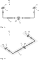
- Fig. 1a shows a schematic diagram illustrating the bottom side 100b of a substrate 100 of an apparatus 200 according to the disclosure forming a 1x2 combiner/divider device.
- the substrate 100 is a dielectric substrate 100 having a top side 100a and a bottom side 100b opposing the top side 100a.
- the bottom side 100b of the substrate 100 is shown.
- An exemplary number of three metal patches 111, 112, 113 are placed at the bottom side 100b of the substrate 100. These metal patches 111, 112, 113 are placed below a waveguide feeding terminal 103 and two waveguide transition terminals 101, 102 of a stripline 121 placed on the top side 100a of the substrate 100 as shown in Figure 1b .
- the metal patches 111, 112, 113 are configured to shape a coupling of the electrical signal with the radio frequency signal in order to match the stripline 121 to the waveguide 210 which is shown in Figure 2 .
- the metal patches 111, 112, 113 may be rectangular shaped as shown in Figure 1a .
- the metal patches 111, 112, 113 may be made of Copper, for example.
- the substrate 100 may be a printed circuit board (PCB) comprising a top side metallization and a bottom side metallization.
- the stripline 121 as shown in Figure 1b may be formed as an etched signal trace within the top side metallization.
- the metal patches 111, 112, 113 may be formed as etched metal islands within the bottom side metallization.
- An upper ground plane (not shown in Figure 1b ) may be arranged above the top side 100a of the substrate 100 outside an outline 130 of the etched signal trace.
- a lower ground plane (not shown in Figure 1a ) may be arranged below the bottom side 100b of the substrate 100 outside an outline 130 of the etched metal island.
- a series of vias (not shown in Figures 1a and 1b ) may electrically connect the upper ground plane with the lower ground plane.
- Fig. 1b shows a schematic diagram illustrating the top side 100a of the substrate 100 of the apparatus 200.
- the substrate 100 is a dielectric substrate 100 having a top side 100a and a bottom side 100b opposing the top side 100a.
- the top side 100a of the substrate 100 is shown.
- a stripline 121 is placed at the top side 100a of the substrate 100.
- the stripline 121 comprises a waveguide feeding terminal 103 for feeding the apparatus 200 with an electrical signal and an exemplary number of two waveguide transition terminals 101, 102 for transition of the electrical signal into a radio frequency signal via a waveguide 210 (shown in Figure 2 ).
- the metal patches 111, 112, 113 shown in Figure 1a are placed at the bottom side 100b of the substrate 100 below the waveguide feeding terminal 103 and the two waveguide transition terminals 101, 102.
- the metal patches 111, 112, 113 are configured to shape a coupling of the electrical signal with the radio frequency signal in order to match the stripline 121 to the waveguide 210 (shown in Figure 2 ).
- a waveguide 210 (shown in Figure 2 ) can be attached to the substrate 100 as shown in Figure 2 .
- the waveguide 210 may be a stepless waveguide having a constant cross-section.
- the waveguide feeding terminal 103 and the two waveguide transition terminals 101, 102 may be formed as inductive fingers, e.g., like a hook as can be seen from Figure 1b .
- the metal patches 111, 112, 113 on the bottom side 100b of the substrate 100 as shown in Figure 1a may form a capacitive component interacting with a respective inductive finger of the stripline 121 to form an impedance of the waveguide feeding terminal 103 and the two waveguide transition terminals 101, 102.
- the inductive fingers of the two waveguide transition terminals 101, 102 are aligned to point into the same direction, e.g., on the right side of the picture as shown in Figure 1b .
- the stripline 121 may be or may comprise a suspended-stripline (SSL).
- the waveguide 210 may be or may comprise a double-ridge waveguide as shown in Figure 2 , for example.
- the substrate 100 can be a printed circuit board comprising a top side metallization and a bottom side metallization.
- the stripline 121 may be formed as an etched signal trace within the top side metallization and the metal patches 111, 112, 113 (shown in Figure 1a ) may be formed as etched metal islands within the bottom side metallization.
- the waveguide transition terminals 101, 102 are two waveguide transition terminals 101, 102 which form the apparatus as a 1-to-2 combiner-divider device 200 (see Figure 2 ).
- the stripline 121 comprises a plurality of stepped sections 121a, 121b which are designed for shaping an impedance of the waveguide feeding terminal 103 and the two waveguide transition terminals 101, 102.
- the stepped sections 121a, 121b are designed for a matching of the stripline 121 with the waveguide 210. Note that only two of these stepped sections are referred to by reference signs 121a, 121b. The other stepped sections without reference signs are also contributing to the design of the stripline 121 characteristics.
- Fig. 1c shows a schematic diagram illustrating the location of the metal patches 111, 112, 113 in relation to the stripline 121 without the substrate 100 in between.
- the metal patches 111, 112, 113 are placed at the bottom side 100b of the substrate 100 below the waveguide feeding terminal 103 and the two waveguide transition terminals 101, 102. That means, the first metal patch 111 is placed below the first waveguide transition terminal 101, the second metal patch 112 is placed below the second waveguide transition terminal 102 and the third metal patch 113 is placed below the waveguide feeding terminal 103.
- a size of the metal patches 111, 112, 113 is optimized with respect to an optimal match of the stripline 121 to the waveguide 210 (shown in Figure 2 ).
- the metal patches 111, 112, 113 fit below the hooked section of the respective terminals 101, 102, 103.
- the stripline 121 shown in Figure 1c has two parts, one part extending from the waveguide feeding terminal 103 to the first waveguide transition terminal 101 and a second part extending from the waveguide feeding terminal 103 to the second waveguide transition terminal 102. Both parts of the stripline 121 are symmetrically in order to implement a symmetrically operating 1x2 combiner/divider device.
- Fig. 1d shows a 3-dimensional view of a 1x2 SSL to double ridged waveguide RF PCB of the apparatus 200.
- the dielectric substrate 100 has a top side 100a and a bottom side 100b.
- the stripline 121 is placed at the top side 100a of the substrate 100 and the metal patches 111, 112, 113 are placed at the bottom side 100b of the substrate 100 or vice versa.
- the stripline 121 comprises a waveguide feeding terminal 103 for feeding the apparatus 200 (shown in Figure 2 ) with an electrical signal and at least one waveguide transition terminal 101, 102 for transition of the electrical signal into a radio frequency signal via a waveguide 210.
- the metal patches 111, 112, 113 are placed at the bottom side 100b of the substrate 100 below the waveguide feeding terminal 103 and the waveguide transition terminals 101, 102.
- the metal patches 111, 112, 113 are configured to shape a coupling of the electrical signal with the radio frequency signal in order to match the stripline 121 to the waveguide 210.
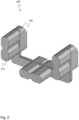
- Fig. 2 shows a 3-dimensional view of a 1x2 SSL to double ridged waveguide 200 according to an embodiment.
- the apparatus 200 which is here a 1x2 SSL to double ridged waveguide 200 comprises a dielectric substrate 100 as described above with respect to Figures 1a to 1d and a waveguide 210 attached to the substrate 100.
- the waveguide 210 is a stepless waveguide having a constant cross section.
- the waveguide 210 encloses the substrate 100 from both sides 100a and 100b of the substrate 100 to form a sandwich-like structure.
- Fig. 3 shows an exemplary frequency response of the 1x2 SSL to double ridged waveguide 200.
- the Figure 3 shows the typical frequency response of the 1x2 divider with uniform waveguide as a result of introducing the capacitive patches 111, 112, 113 as described above with respect to Figures 1a to 1d and 2 to improve the match of the divider.
- the first S-parameter S1,1 is denoted by reference sign 301 and the second S-parameter S2,1 is denoted by reference sign 302.
- the first S-parameter S1,1 is below -20dB between 17.7GHz and 20.2GHz, and 27.5GHz and 30GHz.
- the second S-parameter S2,1 is at about -3dB over the whole shown frequency range between 17.7 GHz and 31 GHz.
- Fig. 4a shows a schematic diagram illustrating the bottom side 400b of a substrate 400 of an apparatus 500 (shown in Figure 5 ) according to the disclosure forming a 1x4 combiner/divider device.
- the substrate 400 is a dielectric substrate 400 having a top side 400a and a bottom side 400b opposing the top side 400a.
- the bottom side 400b of the substrate 400 is shown.
- An exemplary number of five metal patches 111, 112, 113, 114, 115 are placed at the bottom side 400b of the substrate 400. These metal patches 111, 112, 113, 114, 115 are placed below a waveguide feeding terminal 103 and four waveguide transition terminals 101, 102, 104, 105 of a stripline 121 placed on the top side 400a of the substrate 400 as shown in Figure 4b .
- the metal patches 111, 112, 113, 114, 115 are configured to shape a coupling of the electrical signal with the radio frequency signal in order to match the stripline 121 to the waveguide 510 which is shown in Figure 5 .
- the metal patches 111, 112, 113, 114, 115 may be rectangular shaped as shown in Figure 4a .
- the metal patches 111, 112, 113, 114, 115 may be made of Copper, for example.
- the substrate 400 may be a printed circuit board (PCB) comprising a top side metallization and a bottom side metallization.
- the stripline 121 as shown in Figure 4b may be formed as an etched signal trace within the top side metallization.
- the metal patches 111, 112, 113, 114, 115 may be formed as etched metal islands within the bottom side metallization.
- An upper ground plane (not shown in Figure 4b ) may be arranged above the top side 400a of the substrate 400 outside an outline 430 of the etched signal trace.
- a lower ground plane (not shown in Figure 4a ) may be arranged below the bottom side 400b of the substrate 400 outside an outline 430 of the etched metal island.
- a series of vias (not shown in Figures 4a and 4b ) may electrically connect the upper ground plane with the lower ground plane.
- Fig. 4b shows a schematic diagram illustrating the top side 400a of the substrate 400 of the apparatus 500.
- the substrate 400 is a dielectric substrate 400 having a top side 400a and a bottom side 400b opposing the top side 400a.
- the top side 400a of the substrate 400 is shown.
- a stripline 121 is placed at the top side 400a of the substrate 400.
- the stripline 121 comprises a waveguide feeding terminal 103 for feeding the apparatus 200 with an electrical signal and an exemplary number of four waveguide transition terminals 101, 102, 104, 105 for transition of the electrical signal into a radio frequency signal via a waveguide 510 (shown in Figure 5 ).
- the metal patches 111, 112, 113, 114, 115 shown in Figure 4a are placed at the bottom side 400b of the substrate 400 below the waveguide feeding terminal 103 and the four waveguide transition terminals 101, 102, 104, 105.
- the metal patches 111, 112, 113, 114, 115 are configured to shape a coupling of the electrical signal with the radio frequency signal in order to match the stripline 121 to the waveguide 510 (shown in Figure 5 ).
- the waveguide 510 (shown in Figure 5 ) can be attached to the substrate 400 as shown in Figure 5 .
- the waveguide 510 may be a stepless waveguide having a constant cross-section.
- the waveguide feeding terminal 103 and the four waveguide transition terminals 101, 102, 104, 105 may be formed as inductive fingers, e.g. like a hook as can be seen from Figure 4b .
- the metal patches 111, 112, 113, 114, 115 on the bottom side 400b of the substrate 400 as shown in Figure 4a may form a capacitive component interacting with a respective inductive finger of the stripline 121 to form an impedance of the waveguide feeding terminal 103 and the four waveguide transition terminals 101, 102, 104, 105.
- the inductive fingers of the four waveguide transition terminals 101, 102, 104, 105 are aligned to point into the same direction, e.g., on the right side of the picture as shown in Figure 4b .
- Fig. 4c shows a schematic diagram illustrating the location of the metal patches 111, 112, 113, 114, 115 in relation to the stripline 121 without the substrate 400 in between.
- the metal patches 111, 112, 113, 114, 115 are placed at the bottom side 400b of the substrate 400 below the waveguide feeding terminal 103 and the four waveguide transition terminals 101, 102, 104, 105. That means, the first metal patch 111 is placed below the first waveguide transition terminal 101, the second metal patch 112 is placed below the second waveguide transition terminal 102, the third metal patch 113 is placed below the waveguide feeding terminal 103, the fourth metal patch 114 is placed below the third waveguide transition terminal 104 and the fifth metal patch 115 is placed below the fourth waveguide transition terminal 105.
- a size of the metal patches 111, 112, 113, 114, 115 is optimized with respect to an optimal match of the stripline 121 to the waveguide 510 (shown in Figure 5 ).
- the metal patches 111, 112, 113, 114, 115 fit below the hooked section of the respective terminals 101, 102, 103, 104, 105.
- the stripline 121 shown in Figure 4c has two parts, each part having two branches.
- the first part is extending from the waveguide feeding terminal 103 to the first waveguide transition terminal 101 and the third waveguide transition terminal 104, wherein a first branch is branching to the first waveguide transition terminal 101 and a second branch is branching to the third waveguide transition terminal 104.
- the second part is extending from the waveguide feeding terminal 103 to the second waveguide transition terminal 102 and the fourth waveguide transition terminal 105, wherein a first branch is branching to the second waveguide transition terminal 102 and a second branch is branching to the fourth waveguide transition terminal 105
- Both parts of the stripline 121 are symmetrically formed and each branch of a respective part is symmetrically formed in order to implement a symmetrically operating 1x4 combiner/divider device.
- Fig. 4d shows a 3-dimensional view of a 1x4 SSL to double ridged waveguide RF PCB 400 of the apparatus 500.
- the dielectric substrate 400 has a top side 400a and a bottom side 400b.
- the stripline 121 is placed at the top side 400a of the substrate 400 and the metal patches 111, 112, 113, 114, 115 are placed at the bottom side 400b of the substrate 400 or vice versa.
- the stripline 121 comprises a waveguide feeding terminal 103 for feeding the apparatus 500 (shown in Figure 5 ) with an electrical signal and at least one waveguide transition terminal 101, 102, 104, 105 for transition of the electrical signal into a radio frequency signal via a waveguide 510.
- the metal patches 111, 112, 113, 114, 115 are placed at the bottom side 400b of the substrate 400 below the waveguide feeding terminal 103 and the waveguide transition terminals 101, 102, 104, 105.
- the metal patches 111, 112, 113, 114, 115 are configured to shape a coupling of the electrical signal with the radio frequency signal in order to match the stripline 121 to the waveguide 510.
- Fig. 5 shows a 3-dimensional view of a 1x4 SSL to double ridged waveguide 500 according to an embodiment.
- the apparatus 500 which is here a 1x2 SSL to double ridged waveguide 500 comprises a dielectric substrate 400 as described above with respect to Figures 4a to 4d and a waveguide 510 attached to the substrate 400.
- the waveguide 510 is a stepless waveguide having a constant cross section.
- the waveguide 510 encloses the substrate 400 from both sides 400a and 400b of the substrate 400 to form a sandwich-like structure.
- Fig. 6 shows an exemplary frequency response of the 1x4 SSL to double ridged waveguide 500.
- Figure 6 shows the typical frequency response of the 1x4 divider with uniform waveguide as a result of introducing the capacitive patches 111, 112, 113, 114, 115 as described above with respect to Figures 4a to 4d and 5 to improve the match of the divider.
- the first S-parameter S1,1 is denoted by reference sign 601.
- the third S-parameter S3,1 and the second S-parameter S2,1 are denoted by reference sign 603.
- S11 is below -25dB between 17.7GHz to 20.2 GHz and less than -30dB between 27.5GHz to 30GHz.
- the third S-parameter S3,1 and the second S-parameter S2,1 are at about -6dB over the whole shown frequency range between 17.7 GHz and 31 GHz.
- Fig. 7a shows a schematic diagram illustrating waveguide depth reduction over a waveguide 700a having a one-step waveguide cross section.
- the step profile 711, 712 of the waveguide 700a with one step 701 between both waveguide sections 711, 712 as shown in Figure 7a can be reduced to a step-less waveguide resulting in a length reduction of about 0.265 ⁇ .
- Fig. 7b shows a schematic diagram illustrating waveguide depth reduction over a waveguide having a two-step waveguide cross section.
- the step profile 711, 712, 713 of the waveguide 700b with two steps 702, 703 between the three waveguide sections 711, 712, 713 as shown in Figure 7b can be reduced to a step-less waveguide resulting in a length reduction of about 0.388 ⁇ .
- Fig. 8a shows a schematic diagram illustrating the bottom side 100b of a substrate 800 of an apparatus according to the disclosure forming a 1x1 device.
- the substrate 800 may correspond to one half of the substrate 100 described above with respect to Figures 1a to 1d , which is cut into two halves.
- the substrate 800 is a dielectric substrate 800 having a top side 800a and a bottom side 800b opposing the top side 800a.
- the bottom side 800b of the substrate 800 is shown.
- An exemplary number of two metal patches 111, 113 are placed at the bottom side 800b of the substrate 800. These metal patches 111, 113 are placed below a waveguide feeding terminal 103 and a single waveguide transition terminal 101 of a stripline 121 placed on the top side 800a of the substrate 800 as shown in Figure 8b .
- the metal patches 111, 113 are configured to shape a coupling of the electrical signal with the radio frequency signal in order to match the stripline 121 to the waveguide.
- the metal patches 111 113 may be rectangular shaped as shown in Figure 8a .
- the metal patches 111, 113 may be made of Copper, for example.
- the substrate 800 may be a printed circuit board (PCB) comprising a top side metallization and a bottom side metallization.
- the stripline 121 as shown in Figure 8b may be formed as an etched signal trace within the top side metallization.
- the metal patches 111, 113 may be formed as etched metal islands within the bottom side metallization.
- Fig. 8b shows a schematic diagram illustrating the top side 800a of the substrate 800 of the apparatus.
- the substrate 800 is a dielectric substrate 800 having a top side 800a and a bottom side 800b opposing the top side 800a.
- the top side 800a of the substrate 800 is shown.
- a stripline 121 is placed at the top side 800a of the substrate 800.
- the stripline 121 comprises a waveguide feeding terminal 103 for feeding the apparatus 200 with an electrical signal and a waveguide transition terminal 101 for transition of the electrical signal into a radio frequency signal via a waveguide.
- the waveguide may be similar to one half of the waveguide 210 shown in Figure 2 .
- the metal patches 111, 113 shown in Figure 8a are placed at the bottom side 800b of the substrate 800 below the waveguide feeding terminal 103 and the waveguide transition terminal 101.
- the metal patches 111, 113 are configured to shape a coupling of the electrical signal with the radio frequency signal in order to match the stripline 121 to the waveguide.
- the waveguide can be attached to the substrate 800.
- the waveguide may be a stepless waveguide having a constant cross-section.
Landscapes
- Physics & Mathematics (AREA)
- Engineering & Computer Science (AREA)
- Astronomy & Astrophysics (AREA)
- Aviation & Aerospace Engineering (AREA)
- General Physics & Mathematics (AREA)
- Remote Sensing (AREA)
- Waveguides (AREA)
Abstract
The disclosure relates to an apparatus (200), comprising: a dielectric substrate (100) having a top side (100a) and a bottom side (100b) opposing the top side (100a); a stripline (121) placed at the top side (100a) of the substrate (100), the stripline (121) comprising a waveguide feeding terminal (103) for feeding the apparatus (200) with an electrical signal and at least one waveguide transition terminal (101, 102) for transition of the electrical signal into a radio frequency signal via a waveguide (210); and at least one metal patch (111, 112, 113) placed at the bottom side (100b) of the substrate (100) below at least one of the waveguide feeding terminal (103) and the at least one waveguide transition terminal (101, 102); wherein the at least one metal patch (111, 112, 113) is configured to shape a coupling of the electrical signal with the radio frequency signal in order to match the stripline (121) to the waveguide (210).
Description
- The disclosure relates to a reduced length suspended stripline to double ridge waveguide transition that can be used in an array antenna for aircraft tail-mount applications, in particular in the Ka-band for satellite-based communications. In particular, the disclosure relates to a new improvement to reduce the length of the stepped waveguide Suspended-Stripline (SSL) to Double Ridged Waveguide (WRD) transition by removing the steps.
- Currently available Ka-band array antennas for aircraft tail-mount applications use many Suspended-Stripline (SSL) to double ridge waveguide transitions within the internal feeding network. Multiple steps in the waveguide cross section are required to produce a good match from the SSL transmission line to the waveguide. By these stepped waveguide design, the reflections in this component can be kept low and more RF (radio frequency) energy can be transmitted via this component. Hence, known antenna designs use multiple steps in the waveguide cross section to control the fields in such a way as to provide a good broadband or multiband match. The main disadvantage of such a stepped waveguide design is that multiple steps of the waveguide cross section add to the depth and also the mass of the antenna aperture. The steps in the waveguide add several millimeters to the depth of the antenna aperture which increases the total size of the antenna and finally, the antenna is not fitting within the restricted volume of the customers tail-mount radome. When removing these steps, several millimeters can be deducted from the aperture depth, but the performance of the transition is severely degraded.
- An additional disadvantage of the stepped waveguide is the possibility of very small gaps between the waveguide ridges. This can be a manufacturing issue if the gap is too small. Care has to be taken to ensure that a reasonable cutting tool can fit between the small gap between the waveguide ridges.
- It is the object of this disclosure to provide a compact apparatus for transition between an electrical signal and a radio frequency signal without steps in the waveguide cross section that fits in the restricted volume of the tail-mount radome as specified by the customer without severely degrading its performance.
- This object is achieved by the features of the independent claims. Further implementation forms are apparent from the dependent claims, the description and the figures.
- After investigating a number of possible solutions, the most effective method that was found to restore RF (radio frequency) performance to the shorter transition was to introduce a small rectangular patch of copper on the opposite side of the SSL RF PCB (Printed Circuit Board). This was used for each of the many transitions throughout the aperture. With these patches no steps are required and the waveguide cross section is unmodified and more simple to produce.
- The disclosure is based on the finding that a similar effect as produced by the steps in the waveguide cross section can be obtained by introducing a small rectangular patch of copper on the opposite side of the signal conductor of the SSL PCB. This means that no additional components are required and that the patch can be etched as part of the PCB manufacture that is performed regardless to etch the ground plane geometry of the PCB.
- The patch of copper works by modifying the match of the inductive finger of the SSL in the waveguide region, adding capacitance in the transition region in such a way as to provide a good match and therefore maximum power transfer at the required receive and transmit bands. It is the complex combination of the inductive "finger" and capacitive patch that improves the match between the SSL and waveguide transition region. The precise position and size of each patch is found by automatic optimization, rather than an empirical method.
- The advantage of the invention over the current state of the art is that it allows the antenna to fit within the specified radome as required by the customer. The antenna introduced hereinafter is better performing than a traditional reflector antenna. The disclosed apparatus operates over a broader bandwidth in both receive and transmit bands compared to conventional antennas and offers greater aperture efficiency for the same diameter when compared to a traditional reflector antenna.
- Further advantages are that there is no extra cost in manufacture of the RF PCB, a less complicated machining in Aluminum waveguide parts, reduced antenna aperture depth and reduced antenna aperture mass because it will be thinner. The reason to make the aperture thinner is because the aperture is attached to a positioner which must also fit into the small volume allowed in the aircraft's tail radome. A reduction in height of about 0.265λ at 30GHz was obtained for the single SSL to waveguide. The double SSL to waveguide transition has a reduction in height of about 0.388λ at 30GHz.
- A waveguide as described in this disclosure is a structure that guides waves, such as electromagnetic waves, with minimal loss of energy by restricting the transmission of energy to one direction.
- A ridged waveguide as described in this disclosure is a waveguide with conducting ridges protruding into the center of the waveguide from the top wall or bottom wall or both walls. The ridges are parallel to the short wall of the waveguide. A rectangular waveguide with a single protruding ridge from the top or bottom wall is called a Single Ridged Waveguide. A rectangular waveguide with a ridge from the top and bottom wall is called a Double Ridged Waveguide. Ridged Waveguides have a lower impedance and wider bandwidth in their fundamental mode when compared to regular rectangular waveguides. They also have a lower cut-off frequency and have lower power handling capabilities. Ridged waveguides can be used for impedance matching as they decrease the characteristic impedance of the waveguide. Besides, they offer higher bandwidth in comparison to the conventional waveguides.
- A stripline or stripline circuit as described in this disclosure uses a flat strip of metal which is sandwiched between two parallel ground planes. The insulating material of the substrate forms a dielectric. The width of the strip, the thickness of the substrate and the relative permittivity of the substrate determine the characteristic impedance of the strip which is a transmission line. The central conductor need not be equally spaced between the ground planes. In the general case, the dielectric material may be different above and below the central conductor. To prevent the propagation of unwanted modes, the two ground planes should be shorted together. This can be achieved by a series of vias that may run parallel to the strip on each side.
- A suspended stripline (SSL) as described in this disclosure is etched out on a thin substrate and the entire structure is enclosed. Thus, the stripline is suspended in the metallic structure. The suspended stripline has air as dielectric on both sides. The suspended stripline configuration supports pure TEM mode propagation. The SSL has the following advantages: No spurious radiation; wider bandwidth of operation; low losses; and high Q factor.
- A metal patch is described in this disclosure. The metal patch is a planar sheet of metal or metal foil of various shapes on the surface of a substrate, e.g., a printed circuit board (PCB). The metal patch can be rectangular shaped and can be made of Copper, for example.
- In this disclosure communication in the Ka-band is described. Specifically, the frequency range of the Ka-band, as defined by the IEEE system, is from 26 to 40 GHz, with a wavelength of 11.5mm at 26 GHz and 7.5mm at 40 GHz in free space. The Ka-band spectrum is widely used for broadband data communications, mobile phone and data applications, and direct-to-home (DTH) broadcasting. Ka-band transceivers, transmitters, and receivers provide high data throughput and bandwidth due to their operation in this Ka-band part of the frequency spectrum. Most High Throughput Satellites (HTS) operating in the Ka-band typically fall within the following Ka-bands: 27.5 - 31 GHz (uplink) and 17.7 - 21.2 GHz (downlink), for a 3.5 GHz bandwidth.
- According to a first aspect, the disclosure relates to an apparatus for transition between an electrical signal and a radio frequency signal, comprising: a dielectric substrate having a top side and a bottom side opposing the top side; a stripline placed at the top side of the substrate, the stripline comprising a waveguide feeding terminal for feeding the apparatus with an electrical signal and at least one waveguide transition terminal for transition of the electrical signal into a radio frequency signal via a waveguide; and at least one metal patch placed at the bottom side of the substrate below at least one of the waveguide feeding terminal and the at least one waveguide transition terminal; wherein the at least one metal patch is configured to shape a coupling of the electrical signal with the radio frequency signal in order to match the stripline to the waveguide.
- Such apparatus can be very compact due to the missing steps in the waveguide cross section such that is fits in the restricted volume of the tail-mount radome as specified by the customer without severely degrading its performance.
- By introducing the metal patches on the opposite side of the substrate no steps are required and the waveguide cross section can be unmodified and more simple to produce. The metal patches can produce a similar effect than the steps in the waveguide cross section. Hence, no additional components are required and both, size and weight of the waveguide can be reduced without degrading the performance.
- In an exemplary implementation of the apparatus, the apparatus comprises a waveguide attached to the substrate, wherein the waveguide is a stepless waveguide having a constant cross-section.
- This provides the advantage that a stepless waveguide with constant cross-section can have a reduced length compared to a stepped waveguide, thereby fitting in the restricted space of the tail-mount radome. By the introduced metal patches, the performance of the apparatus is not decreased.
- In an exemplary implementation of the apparatus, the waveguide feeding terminal and the at least one waveguide transition terminal are formed as inductive fingers; wherein the at least one metal patch forms a capacitive component interacting with a respective inductive finger to form an impedance of the waveguide feeding terminal and the at least one waveguide transition terminal.
- This provides the advantage that the inductive component of the fingers and the capacitive component of the metal patches can be adjusted by design in order to obtain a match of the stripline to the waveguide resulting in an improved antenna gain.
- An inductive finger describes a protruding section of the stripline that provides an inductive component. The inductive finger may be formed as a hook, for example. At the inductive finger, a course of the line may vary between different directions in order to implement the inductive component.
- In an exemplary implementation of the apparatus, the inductive fingers of at least two waveguide transition terminals are aligned to point into the same direction.
- This provides the advantage that a phase of each waveguide transition terminal can be equal. Thus, an improved antenna array can be designed with multiple such apparatuses.
- In an exemplary implementation of the apparatus, the at least one metal patch is rectangular shaped.
- This provides the advantage that the metal patch can be easily manufactured, e.g., by cutting a metal foil into smaller parts.
- In an exemplary implementation of the apparatus, the stripline comprises a suspended-stripline; and/or the waveguide comprises a double-ridge waveguide.
- Such suspended-stripline provides the advantages of no spurious radiation, wider bandwidth of operation, low losses and high Q factor. The double-ridge waveguide provides the advantage of a low impedance and wide bandwidth in its fundamental mode when compared to a regular rectangular waveguide. The double-ridge waveguide also has a lower cut-off frequency and lower power handling capabilities. The double-ridge waveguide can be efficiently used for impedance matching as it decreases the characteristic impedance of the waveguide. Besides, the double-ridge waveguide offers higher bandwidth in comparison to a regular rectangular waveguide.
- In an exemplary implementation of the apparatus, the substrate is a printed circuit board comprising a top side metallization and a bottom side metallization; and the stripline is formed as an etched signal trace within the top side metallization and the at least one metal patch is formed as an etched metal island within the bottom side metallization.
- This provides the advantage that the apparatus can be easily manufactured when using a printed circuit board. The manufacturing steps for producing the stripline and the metal patches can be efficiently performed by a production machine.
- In an exemplary implementation of the apparatus, the apparatus comprises: an upper ground plane arranged above the top side of the substrate outside an outline of the etched signal trace; a lower ground plane arranged below the bottom side of the substrate outside an outline of the etched metal island; and a series of vias electrically connecting the upper ground plane with the lower ground plane.
- This provides the advantage that a suspended stripline can be easily manufactured. This suspended stripline configuration supports pure TEM mode propagation and provides the advantages of no spurious radiation, wider bandwidth of operation, low losses and high Q factor.
- In an exemplary implementation of the apparatus, the at least one waveguide transition terminal comprises: two waveguide transition terminals forming the apparatus as a 1-to-2 combiner-divider device; four waveguide transition terminals forming the apparatus as a 1-to-4 combiner-divider device; or a single waveguide transition terminal forming the apparatus as a 1-to-1 coupling device.
- This provides the advantage that apparatus can be flexibly designed according to the needs of the customer, e.g., as one of the above configurations, including a 1-to-2 combiner-divider device, a 1-to-4 combiner-divider device or a 1-to-1 coupling device. Higher stage combiner-divider devices can be implemented by using multiple such devices.
- In an exemplary implementation of the apparatus, the stripline comprises stepped sections, the stepped sections shaping an impedance of the waveguide feeding terminal and the at least one waveguide transition terminal.
- This provides the advantage that the impedance can be shaped for an improved match of the stripline to the waveguide, hence improving the antenna gain.
- Further examples will be described with respect to the following figures, in which:
-
Fig. 1a shows a schematic diagram illustrating thebottom side 100b of asubstrate 100 of anapparatus 200 according to the disclosure forming a 1x2 combiner/divider device; -
Fig. 1b shows a schematic diagram illustrating thetop side 100a of thesubstrate 100 of theapparatus 200; -
Fig. 1c shows a schematic diagram illustrating the location of themetal patches stripline 121 without thesubstrate 100 in between; -
Fig. 1d shows a 3-dimensional view of a 1x2 SSL to double ridgedwaveguide RF PCB 100 of theapparatus 200; -
Fig. 2 shows a 3-dimensional view of a 1x2 SSL to double ridgedwaveguide 200 according to an embodiment; -
Fig. 3 shows an exemplary frequency response of the 1x2 SSL to double ridgedwaveguide 200; -
Fig. 4a shows a schematic diagram illustrating thebottom side 400b of asubstrate 400 of anapparatus 500 according to the disclosure forming a 1x4 combiner/divider device; -
Fig. 4b shows a schematic diagram illustrating thetop side 400a of thesubstrate 400 of theapparatus 500; -
Fig. 4c shows a schematic diagram illustrating the location of themetal patches stripline 121 without thesubstrate 400 in between; -
Fig. 4d shows a 3-dimensional view of a 1x4 SSL to double ridgedwaveguide RF PCB 400 of theapparatus 500; -
Fig. 5 shows a 3-dimensional view of a 1x4 SSL to double ridgedwaveguide 500 according to an embodiment; -
Fig. 6 shows an exemplary frequency response of the 1x4 SSL to double ridgedwaveguide 500; -
Fig. 7a shows a schematic diagram illustrating waveguide depth reduction over a waveguide having a one-step waveguide cross section; -
Fig. 7b shows a schematic diagram illustrating waveguide depth reduction over a waveguide having a two-step waveguide cross section; -
Fig. 8a shows a schematic diagram illustrating thebottom side 800b of asubstrate 800 of an apparatus according to the disclosure forming a 1x1 coupling device; and -
Fig. 8b shows a schematic diagram illustrating thetop side 800a of thesubstrate 800 of the apparatus. - In the following detailed description, reference is made to the accompanying drawings, which form a part thereof, and in which is shown by way of illustration specific aspects in which the disclosure may be practiced. It is understood that other aspects may be utilized and structural or logical changes may be made without departing from the scope of the present disclosure. The following detailed description, therefore, is not to be taken in a limiting sense, and the scope of the present disclosure is defined by the appended claims.
- It is understood that comments made in connection with a described method may also hold true for a corresponding device or system configured to perform the method and vice versa. Further, it is understood that the features of the various exemplary aspects described herein may be combined with each other, unless specifically noted otherwise.
-
Fig. 1a shows a schematic diagram illustrating thebottom side 100b of asubstrate 100 of anapparatus 200 according to the disclosure forming a 1x2 combiner/divider device. - The
substrate 100 is adielectric substrate 100 having atop side 100a and abottom side 100b opposing thetop side 100a. InFigure 1a , thebottom side 100b of thesubstrate 100 is shown. An exemplary number of threemetal patches bottom side 100b of thesubstrate 100. Thesemetal patches waveguide feeding terminal 103 and twowaveguide transition terminals stripline 121 placed on thetop side 100a of thesubstrate 100 as shown inFigure 1b . - The
metal patches stripline 121 to thewaveguide 210 which is shown inFigure 2 . - The
metal patches Figure 1a . Themetal patches - The
substrate 100 may be a printed circuit board (PCB) comprising a top side metallization and a bottom side metallization. Thestripline 121 as shown inFigure 1b may be formed as an etched signal trace within the top side metallization. Themetal patches - An upper ground plane (not shown in
Figure 1b ) may be arranged above thetop side 100a of thesubstrate 100 outside anoutline 130 of the etched signal trace. A lower ground plane (not shown inFigure 1a ) may be arranged below thebottom side 100b of thesubstrate 100 outside anoutline 130 of the etched metal island. A series of vias (not shown inFigures 1a and 1b ) may electrically connect the upper ground plane with the lower ground plane. -
Fig. 1b shows a schematic diagram illustrating thetop side 100a of thesubstrate 100 of theapparatus 200. - As described above, the
substrate 100 is adielectric substrate 100 having atop side 100a and abottom side 100b opposing thetop side 100a. InFigure 1b , thetop side 100a of thesubstrate 100 is shown. Astripline 121 is placed at thetop side 100a of thesubstrate 100. Thestripline 121 comprises awaveguide feeding terminal 103 for feeding theapparatus 200 with an electrical signal and an exemplary number of twowaveguide transition terminals Figure 2 ). - The
metal patches Figure 1a are placed at thebottom side 100b of thesubstrate 100 below thewaveguide feeding terminal 103 and the twowaveguide transition terminals - The
metal patches stripline 121 to the waveguide 210 (shown inFigure 2 ). - A waveguide 210 (shown in
Figure 2 ) can be attached to thesubstrate 100 as shown inFigure 2 . Thewaveguide 210 may be a stepless waveguide having a constant cross-section. - As shown in
Figure 1b , thewaveguide feeding terminal 103 and the twowaveguide transition terminals Figure 1b . Themetal patches bottom side 100b of thesubstrate 100 as shown inFigure 1a may form a capacitive component interacting with a respective inductive finger of thestripline 121 to form an impedance of thewaveguide feeding terminal 103 and the twowaveguide transition terminals - As shown in
Figure 1b , the inductive fingers of the twowaveguide transition terminals Figure 1b . - The
stripline 121 may be or may comprise a suspended-stripline (SSL). Thewaveguide 210 may be or may comprise a double-ridge waveguide as shown inFigure 2 , for example. - The
substrate 100 can be a printed circuit board comprising a top side metallization and a bottom side metallization. Thestripline 121 may be formed as an etched signal trace within the top side metallization and themetal patches Figure 1a ) may be formed as etched metal islands within the bottom side metallization. - In the example shown in
Figures 1a to 1d and2 , thewaveguide transition terminals waveguide transition terminals Figure 2 ). - As can be seen in
Figure 1b , thestripline 121 comprises a plurality of steppedsections waveguide feeding terminal 103 and the twowaveguide transition terminals sections stripline 121 with thewaveguide 210. Note that only two of these stepped sections are referred to byreference signs stripline 121 characteristics. -
Fig. 1c shows a schematic diagram illustrating the location of themetal patches stripline 121 without thesubstrate 100 in between. - As can be seen from
Figure 1c , themetal patches bottom side 100b of thesubstrate 100 below thewaveguide feeding terminal 103 and the twowaveguide transition terminals first metal patch 111 is placed below the firstwaveguide transition terminal 101, thesecond metal patch 112 is placed below the secondwaveguide transition terminal 102 and thethird metal patch 113 is placed below thewaveguide feeding terminal 103. - A size of the
metal patches stripline 121 to the waveguide 210 (shown inFigure 2 ). - In this example of
Figure 1c , themetal patches respective terminals - The
stripline 121 shown inFigure 1c has two parts, one part extending from thewaveguide feeding terminal 103 to the firstwaveguide transition terminal 101 and a second part extending from thewaveguide feeding terminal 103 to the secondwaveguide transition terminal 102. Both parts of thestripline 121 are symmetrically in order to implement a symmetrically operating 1x2 combiner/divider device. -
Fig. 1d shows a 3-dimensional view of a 1x2 SSL to double ridged waveguide RF PCB of theapparatus 200. - As described above, the
dielectric substrate 100 has atop side 100a and abottom side 100b. Thestripline 121 is placed at thetop side 100a of thesubstrate 100 and themetal patches bottom side 100b of thesubstrate 100 or vice versa. - The
stripline 121 comprises awaveguide feeding terminal 103 for feeding the apparatus 200 (shown inFigure 2 ) with an electrical signal and at least onewaveguide transition terminal waveguide 210. - The
metal patches bottom side 100b of thesubstrate 100 below thewaveguide feeding terminal 103 and thewaveguide transition terminals - The
metal patches stripline 121 to thewaveguide 210. -
Fig. 2 shows a 3-dimensional view of a 1x2 SSL to double ridgedwaveguide 200 according to an embodiment. - The
apparatus 200 which is here a 1x2 SSL to double ridgedwaveguide 200 comprises adielectric substrate 100 as described above with respect toFigures 1a to 1d and awaveguide 210 attached to thesubstrate 100. Thewaveguide 210 is a stepless waveguide having a constant cross section. - The
waveguide 210 encloses thesubstrate 100 from bothsides substrate 100 to form a sandwich-like structure. -
Fig. 3 shows an exemplary frequency response of the 1x2 SSL to double ridgedwaveguide 200. - The
Figure 3 shows the typical frequency response of the 1x2 divider with uniform waveguide as a result of introducing thecapacitive patches Figures 1a to 1d and2 to improve the match of the divider. - The first S-parameter S1,1 is denoted by
reference sign 301 and the second S-parameter S2,1 is denoted byreference sign 302. - The first S-parameter S1,1 is below -20dB between 17.7GHz and 20.2GHz, and 27.5GHz and 30GHz.
- The second S-parameter S2,1 is at about -3dB over the whole shown frequency range between 17.7 GHz and 31 GHz.
-
Fig. 4a shows a schematic diagram illustrating thebottom side 400b of asubstrate 400 of an apparatus 500 (shown inFigure 5 ) according to the disclosure forming a 1x4 combiner/divider device. - Similar to the description of
Figures 1a to 1d , thesubstrate 400 is adielectric substrate 400 having atop side 400a and abottom side 400b opposing thetop side 400a. InFigure 4a , thebottom side 400b of thesubstrate 400 is shown. An exemplary number of fivemetal patches bottom side 400b of thesubstrate 400. Thesemetal patches waveguide feeding terminal 103 and fourwaveguide transition terminals stripline 121 placed on thetop side 400a of thesubstrate 400 as shown inFigure 4b . - The
metal patches stripline 121 to thewaveguide 510 which is shown inFigure 5 . - The
metal patches Figure 4a . Themetal patches - The
substrate 400 may be a printed circuit board (PCB) comprising a top side metallization and a bottom side metallization. Thestripline 121 as shown inFigure 4b may be formed as an etched signal trace within the top side metallization. Themetal patches - An upper ground plane (not shown in
Figure 4b ) may be arranged above thetop side 400a of thesubstrate 400 outside anoutline 430 of the etched signal trace. A lower ground plane (not shown inFigure 4a ) may be arranged below thebottom side 400b of thesubstrate 400 outside anoutline 430 of the etched metal island. A series of vias (not shown inFigures 4a and 4b ) may electrically connect the upper ground plane with the lower ground plane. -
Fig. 4b shows a schematic diagram illustrating thetop side 400a of thesubstrate 400 of theapparatus 500. - As described above, the
substrate 400 is adielectric substrate 400 having atop side 400a and abottom side 400b opposing thetop side 400a. InFigure 4b , thetop side 400a of thesubstrate 400 is shown. Astripline 121 is placed at thetop side 400a of thesubstrate 400. Thestripline 121 comprises awaveguide feeding terminal 103 for feeding theapparatus 200 with an electrical signal and an exemplary number of fourwaveguide transition terminals Figure 5 ). - The
metal patches Figure 4a are placed at thebottom side 400b of thesubstrate 400 below thewaveguide feeding terminal 103 and the fourwaveguide transition terminals - The
metal patches stripline 121 to the waveguide 510 (shown inFigure 5 ). - The waveguide 510 (shown in
Figure 5 ) can be attached to thesubstrate 400 as shown inFigure 5 . Thewaveguide 510 may be a stepless waveguide having a constant cross-section. - As shown in
Figure 4b , thewaveguide feeding terminal 103 and the fourwaveguide transition terminals Figure 4b . Themetal patches bottom side 400b of thesubstrate 400 as shown inFigure 4a may form a capacitive component interacting with a respective inductive finger of thestripline 121 to form an impedance of thewaveguide feeding terminal 103 and the fourwaveguide transition terminals - As shown in
Figure 4b , the inductive fingers of the fourwaveguide transition terminals Figure 4b . -
Fig. 4c shows a schematic diagram illustrating the location of themetal patches stripline 121 without thesubstrate 400 in between. - As can be seen from
Figure 4c , themetal patches bottom side 400b of thesubstrate 400 below thewaveguide feeding terminal 103 and the fourwaveguide transition terminals first metal patch 111 is placed below the firstwaveguide transition terminal 101, thesecond metal patch 112 is placed below the secondwaveguide transition terminal 102, thethird metal patch 113 is placed below thewaveguide feeding terminal 103, thefourth metal patch 114 is placed below the thirdwaveguide transition terminal 104 and thefifth metal patch 115 is placed below the fourthwaveguide transition terminal 105. - A size of the
metal patches stripline 121 to the waveguide 510 (shown inFigure 5 ). - In this example of
Figure 4c , themetal patches respective terminals - The
stripline 121 shown inFigure 4c has two parts, each part having two branches. The first part is extending from thewaveguide feeding terminal 103 to the firstwaveguide transition terminal 101 and the thirdwaveguide transition terminal 104, wherein a first branch is branching to the firstwaveguide transition terminal 101 and a second branch is branching to the thirdwaveguide transition terminal 104. The second part is extending from thewaveguide feeding terminal 103 to the secondwaveguide transition terminal 102 and the fourthwaveguide transition terminal 105, wherein a first branch is branching to the secondwaveguide transition terminal 102 and a second branch is branching to the fourthwaveguide transition terminal 105 Both parts of thestripline 121 are symmetrically formed and each branch of a respective part is symmetrically formed in order to implement a symmetrically operating 1x4 combiner/divider device. -
Fig. 4d shows a 3-dimensional view of a 1x4 SSL to double ridgedwaveguide RF PCB 400 of theapparatus 500. - As described above, the
dielectric substrate 400 has atop side 400a and abottom side 400b. Thestripline 121 is placed at thetop side 400a of thesubstrate 400 and themetal patches bottom side 400b of thesubstrate 400 or vice versa. - The
stripline 121 comprises awaveguide feeding terminal 103 for feeding the apparatus 500 (shown inFigure 5 ) with an electrical signal and at least onewaveguide transition terminal waveguide 510. - The
metal patches bottom side 400b of thesubstrate 400 below thewaveguide feeding terminal 103 and thewaveguide transition terminals - The
metal patches stripline 121 to thewaveguide 510. -
Fig. 5 shows a 3-dimensional view of a 1x4 SSL to double ridgedwaveguide 500 according to an embodiment. - The
apparatus 500 which is here a 1x2 SSL to double ridgedwaveguide 500 comprises adielectric substrate 400 as described above with respect toFigures 4a to 4d and awaveguide 510 attached to thesubstrate 400. Thewaveguide 510 is a stepless waveguide having a constant cross section. - The
waveguide 510 encloses thesubstrate 400 from bothsides substrate 400 to form a sandwich-like structure. -
Fig. 6 shows an exemplary frequency response of the 1x4 SSL to double ridgedwaveguide 500. -
Figure 6 shows the typical frequency response of the 1x4 divider with uniform waveguide as a result of introducing thecapacitive patches Figures 4a to 4d and5 to improve the match of the divider. - The first S-parameter S1,1 is denoted by
reference sign 601. The third S-parameter S3,1 and the second S-parameter S2,1 are denoted byreference sign 603. - S11 is below -25dB between 17.7GHz to 20.2 GHz and less than -30dB between 27.5GHz to 30GHz.
- The third S-parameter S3,1 and the second S-parameter S2,1 are at about -6dB over the whole shown frequency range between 17.7 GHz and 31 GHz.
-
Fig. 7a shows a schematic diagram illustrating waveguide depth reduction over awaveguide 700a having a one-step waveguide cross section. - By applying the
metal patches step profile waveguide 700a with onestep 701 between bothwaveguide sections Figure 7a can be reduced to a step-less waveguide resulting in a length reduction of about 0.265λ. -
Fig. 7b shows a schematic diagram illustrating waveguide depth reduction over a waveguide having a two-step waveguide cross section. - By applying the
metal patches step profile waveguide 700b with twosteps 702, 703 between the threewaveguide sections Figure 7b can be reduced to a step-less waveguide resulting in a length reduction of about 0.388λ. -
Fig. 8a shows a schematic diagram illustrating thebottom side 100b of asubstrate 800 of an apparatus according to the disclosure forming a 1x1 device. - The
substrate 800 may correspond to one half of thesubstrate 100 described above with respect toFigures 1a to 1d , which is cut into two halves. - The
substrate 800 is adielectric substrate 800 having atop side 800a and abottom side 800b opposing thetop side 800a. InFigure 8a , thebottom side 800b of thesubstrate 800 is shown. An exemplary number of twometal patches bottom side 800b of thesubstrate 800. Thesemetal patches waveguide feeding terminal 103 and a singlewaveguide transition terminal 101 of astripline 121 placed on thetop side 800a of thesubstrate 800 as shown inFigure 8b . - The
metal patches stripline 121 to the waveguide. - The
metal patches 111 113 may be rectangular shaped as shown inFigure 8a . Themetal patches - The
substrate 800 may be a printed circuit board (PCB) comprising a top side metallization and a bottom side metallization. Thestripline 121 as shown inFigure 8b may be formed as an etched signal trace within the top side metallization. Themetal patches -
Fig. 8b shows a schematic diagram illustrating thetop side 800a of thesubstrate 800 of the apparatus. - As described above, the
substrate 800 is adielectric substrate 800 having atop side 800a and abottom side 800b opposing thetop side 800a. InFigure 8b , thetop side 800a of thesubstrate 800 is shown. Astripline 121 is placed at thetop side 800a of thesubstrate 800. Thestripline 121 comprises awaveguide feeding terminal 103 for feeding theapparatus 200 with an electrical signal and awaveguide transition terminal 101 for transition of the electrical signal into a radio frequency signal via a waveguide. The waveguide may be similar to one half of thewaveguide 210 shown inFigure 2 . - The
metal patches Figure 8a are placed at thebottom side 800b of thesubstrate 800 below thewaveguide feeding terminal 103 and thewaveguide transition terminal 101. - The
metal patches stripline 121 to the waveguide. - The waveguide can be attached to the
substrate 800. The waveguide may be a stepless waveguide having a constant cross-section. - While a particular feature or aspect of the disclosure may have been disclosed with respect to only one of several implementations, such feature or aspect may be combined with one or more other features or aspects of the other implementations as may be desired and advantageous for any given or particular application. Furthermore, to the extent that the terms "include", "have", "with", or other variants thereof are used in either the detailed description or the claims, such terms are intended to be inclusive in a manner similar to the term "comprise". Also, the terms "exemplary", "for example" and "e.g." are merely meant as an example, rather than the best or optimal. The terms "coupled" and "connected", along with derivatives may have been used. It should be understood that these terms may have been used to indicate that two elements cooperate or interact with each other regardless whether they are in direct physical or electrical contact, or they are not in direct contact with each other.
- Although specific aspects have been illustrated and described herein, it will be appreciated by those of ordinary skill in the art that a variety of alternate and/or equivalent implementations may be substituted for the specific aspects shown and described without departing from the scope of the present disclosure. This application is intended to cover any adaptations or variations of the specific aspects discussed herein.
- Although the elements in the following claims are recited in a particular sequence with corresponding labeling, unless the claim recitations otherwise imply a particular sequence for implementing some or all of those elements, those elements are not necessarily intended to be limited to being implemented in that particular sequence.
- Many alternatives, modifications, and variations will be apparent to those skilled in the art in light of the above teachings. Of course, those skilled in the art readily recognize that there are numerous applications of the invention beyond those described herein. While the present invention has been described with reference to one or more particular embodiments, those skilled in the art recognize that many changes may be made thereto without departing from the scope of the present invention. It is therefore to be understood that within the scope of the appended claims and their equivalents, the invention may be practiced otherwise than as specifically described herein.
-
- 100
- substrate, e.g. PCB, of an apparatus
- 100a
- top side of substrate
- 100b
- bottom side of substrate
- 101
- first waveguide transition terminal
- 102
- second waveguide transition terminal
- 103
- waveguide feeding terminal
- 104
- third waveguide transition terminal
- 105
- fourth waveguide transition terminal
- 121
- stripline
- 121a, 121b
- stepped sections in stripline
- 111
- first metal patch
- 112
- second metal patch
- 113
- third metal patch
- 114
- fourth metal patch
- 115
- fifth metal patch
- 130
- outline of etched signal trace or outline of etched metal island
- 200
- apparatus implementing a 1-to-2 combiner divider device
- 210
- waveguide
- 400
- substrate, e.g. PCB, of an apparatus implementing a 1-to-4 combiner divider device
- 400a
- top side of substrate
- 400b
- bottom side of substrate
- 430
- outline of etched signal trace or outline of etched metal island
- 500
- apparatus implementing a 1-to-4 combiner divider device
- 510
- waveguide
- 800
- substrate, e.g. PCB, of an apparatus implementing a 1-to-1 coupling device
- 800a
- top side of substrate
- 800b
- bottom side of substrate
Claims (10)
- An apparatus (200) for transition between an electrical signal and a radio frequency signal, the apparatus (200) comprising:a dielectric substrate (100) having a top side (100a) and a bottom side (100b) opposing the top side (100a);a stripline (121) placed at the top side (100a) of the substrate (100), the stripline (121) comprising a waveguide feeding terminal (103) for feeding the apparatus (200) with an electrical signal and at least one waveguide transition terminal (101, 102) for transition of the electrical signal into a radio frequency signal via a waveguide (210); andat least one metal patch (111, 112, 113) placed at the bottom side (100b) of the substrate (100) below at least one of the waveguide feeding terminal (103) and the at least one waveguide transition terminal (101, 102);wherein the at least one metal patch (111, 112, 113) is configured to shape a coupling of the electrical signal with the radio frequency signal in order to match the stripline (121) to the waveguide (210).
- The apparatus (200) of claim 1, comprising:
a waveguide (210) attached to the substrate (100), wherein the waveguide (210) is a stepless waveguide having a constant cross-section. - The apparatus (200) of claim 1 or 2,wherein the waveguide feeding terminal (103) and the at least one waveguide transition terminal (101, 102) are formed as inductive fingers;wherein the at least one metal patch (111, 112, 113) forms a capacitive component interacting with a respective inductive finger to form an impedance of the waveguide feeding terminal (103) and the at least one waveguide transition terminal (101, 102).
- The apparatus (200) of claim 3,
wherein the inductive fingers of at least two waveguide transition terminals (101, 102) are aligned to point into the same direction. - The apparatus (200) of any of the preceding claims,
wherein the at least one metal patch (111, 112, 113) is rectangular shaped. - The apparatus (200) of any of the preceding claims,wherein the stripline (121) comprises a suspended-stripline; and/orwherein the waveguide (210) comprises a double-ridge waveguide.
- The apparatus (200) of any of the preceding claims,wherein the substrate (100) is a printed circuit board comprising a top side metallization and a bottom side metallization; andwherein the stripline (121) is formed as an etched signal trace within the top side metallization and the at least one metal patch (111, 112, 113) is formed as an etched metal island within the bottom side metallization.
- The apparatus (200) of claim 7, comprising:an upper ground plane arranged above the top side (100a) of the substrate (100) outside an outline (130) of the etched signal trace;a lower ground plane arranged below the bottom side (100b) of the substrate (100) outside an outline (130) of the etched metal island; anda series of vias electrically connecting the upper ground plane with the lower ground plane.
- The apparatus (200, 400, 800) of any of the preceding claims,
wherein the at least one waveguide transition terminal (101, 102) comprises:two waveguide transition terminals (101, 102) forming the apparatus as a 1-to-2 combiner-divider device (200);four waveguide transition terminals (101, 102, 104, 105) forming the apparatus as a 1-to-4 combiner-divider device (500); ora single waveguide transition terminal (101) forming the apparatus as a 1-to-1 coupling device. - The apparatus (200) of any of the preceding claims,
wherein the stripline (121) comprises stepped sections (121a, 121b), the stepped sections shaping an impedance of the waveguide feeding terminal (103) and the at least one waveguide transition terminal (101, 102).
Applications Claiming Priority (1)
| Application Number | Priority Date | Filing Date | Title |
|---|---|---|---|
| GB2303382.2A GB2627947B (en) | 2023-03-08 | 2023-03-08 | Reduced length suspended stripline to double ridge waveguide transition |
Publications (1)
| Publication Number | Publication Date |
|---|---|
| EP4429016A1 true EP4429016A1 (en) | 2024-09-11 |
Family
ID=85980190
Family Applications (1)
| Application Number | Title | Priority Date | Filing Date |
|---|---|---|---|
| EP24156848.4A Pending EP4429016A1 (en) | 2023-03-08 | 2024-02-09 | Reduced length suspended stripline to double ridge waveguide transition |
Country Status (4)
| Country | Link |
|---|---|
| US (1) | US20240305012A1 (en) |
| EP (1) | EP4429016A1 (en) |
| CN (1) | CN117937107A (en) |
| GB (1) | GB2627947B (en) |
Citations (4)
| Publication number | Priority date | Publication date | Assignee | Title |
|---|---|---|---|---|
| US20050200424A1 (en) * | 2004-03-11 | 2005-09-15 | Mitsubishi Denki Kabushiki Kaisha | Microstripline waveguide converter |
| JP2012175180A (en) * | 2011-02-17 | 2012-09-10 | Japan Radio Co Ltd | Waveguide transmission line converter |
| US9716321B2 (en) * | 2012-07-03 | 2017-07-25 | Lisa Draexlmaier Gmbh | Antenna system for broadband satellite communication in the GHz frequency range, comprising a feeding arrangement |
| US9761955B2 (en) * | 2014-08-29 | 2017-09-12 | Lisa Draexlmaier Gmbh | Feed network for antenna systems having microstrip conductor loops |
Family Cites Families (8)
| Publication number | Priority date | Publication date | Assignee | Title |
|---|---|---|---|---|
| US8674885B2 (en) * | 2010-08-31 | 2014-03-18 | Siklu Communication ltd. | Systems for interfacing waveguide antenna feeds with printed circuit boards |
| US9520635B2 (en) * | 2013-03-22 | 2016-12-13 | Peraso Technologies Inc. | RF system-in-package with microstrip-to-waveguide transition |
| US10938082B2 (en) * | 2018-08-24 | 2021-03-02 | The Boeing Company | Aperture-coupled microstrip-to-waveguide transitions |
| CN110061337B (en) * | 2019-05-06 | 2023-10-27 | 云南大学 | Directional coupler based on packaged integrated substrate gap waveguide |
| US11201381B1 (en) * | 2020-01-07 | 2021-12-14 | First Rf Corporation | Corporate power splitter with integrated filtering |
| US20220131275A1 (en) * | 2020-10-26 | 2022-04-28 | Microelectronics Technology, Inc. | Apparatus for waveguide transition and antenna array having the same |
| JP7606087B2 (en) * | 2021-03-15 | 2024-12-25 | 富士通株式会社 | Power Combiner |
| US11967764B1 (en) * | 2021-10-22 | 2024-04-23 | Waymo Llc | Single antenna with dual circular polarizations and quad feeds for millimeter wave applications |
-
2023
- 2023-03-08 GB GB2303382.2A patent/GB2627947B/en active Active
-
2024
- 2024-02-09 EP EP24156848.4A patent/EP4429016A1/en active Pending
- 2024-03-06 US US18/597,516 patent/US20240305012A1/en active Pending
- 2024-03-08 CN CN202410265341.5A patent/CN117937107A/en active Pending
Patent Citations (4)
| Publication number | Priority date | Publication date | Assignee | Title |
|---|---|---|---|---|
| US20050200424A1 (en) * | 2004-03-11 | 2005-09-15 | Mitsubishi Denki Kabushiki Kaisha | Microstripline waveguide converter |
| JP2012175180A (en) * | 2011-02-17 | 2012-09-10 | Japan Radio Co Ltd | Waveguide transmission line converter |
| US9716321B2 (en) * | 2012-07-03 | 2017-07-25 | Lisa Draexlmaier Gmbh | Antenna system for broadband satellite communication in the GHz frequency range, comprising a feeding arrangement |
| US9761955B2 (en) * | 2014-08-29 | 2017-09-12 | Lisa Draexlmaier Gmbh | Feed network for antenna systems having microstrip conductor loops |
Also Published As
| Publication number | Publication date |
|---|---|
| CN117937107A (en) | 2024-04-26 |
| GB2627947A (en) | 2024-09-11 |
| US20240305012A1 (en) | 2024-09-12 |
| GB2627947B (en) | 2025-08-06 |
| GB202303382D0 (en) | 2023-04-19 |
Similar Documents
| Publication | Publication Date | Title |
|---|---|---|
| US6133879A (en) | Multifrequency microstrip antenna and a device including said antenna | |
| US7215284B2 (en) | Passive self-switching dual band array antenna | |
| CN113809518B (en) | Microwave and millimeter wave large-frequency ratio common-aperture antenna with high isolation | |
| US9142889B2 (en) | Compact tapered slot antenna | |
| US6121930A (en) | Microstrip antenna and a device including said antenna | |
| CN111052504A (en) | Millimeter wave antenna array element, array antenna and communication product | |
| CN110783704B (en) | Dual-via-probe-fed integrated substrate gap waveguide circularly polarized antenna | |
| WO2019223318A1 (en) | Indoor base station and pifa antenna thereof | |
| CN109980366A (en) | A kind of broadband double-circle polarization endfire array antenna based on gap waveguide | |
| CN110233329B (en) | A Miniaturized High Isolation Common Aperture Antenna Based on Structure Multiplexing | |
| CN202444055U (en) | Microstrip array antenna | |
| CN111987422B (en) | Ultralow-profile multi-frequency broadband antenna and communication equipment | |
| US20250096481A1 (en) | Transmission device and antenna | |
| CN115441170A (en) | A Coplanar Waveguide Dual-polarized Notch Crossed Dipole Antenna with Three Radiating Nulls | |
| CN210668685U (en) | Novel dual-via-hole probe feed ISGW circularly polarized antenna | |
| GB2453160A (en) | Patch antenna with slots | |
| CN113078457A (en) | Double-frequency double-fed high-gain antenna and electronic equipment | |
| US20240305012A1 (en) | Reduced length suspended stripline to double ridge waveguide transition | |
| CN119092996A (en) | A miniaturized broadband 5G millimeter-wave filtering antenna based on substrate-integrated waveguide | |
| Rai et al. | Integrated dielectric resonator antenna to traditional antenna for better bandwidth and gain | |
| CN112271447B (en) | Millimeter wave magnetoelectric dipole antenna | |
| Gupta et al. | Performance Enhancement of 10GHz Patch Antenna using DGS and Perforated Patch Configuration for Advanced Wireless Communication Systems | |
| CN114498019B (en) | Antenna patch, patch antenna, antenna array and electronic equipment | |
| CN220439879U (en) | Multi-frequency single-feed antenna and electronic equipment | |
| RU243188U1 (en) | Dual-Band Low-Profile K/Q-Band Antenna Array with Combined Power Supply System |
Legal Events
| Date | Code | Title | Description |
|---|---|---|---|
| PUAI | Public reference made under article 153(3) epc to a published international application that has entered the european phase |
Free format text: ORIGINAL CODE: 0009012 |
|
| STAA | Information on the status of an ep patent application or granted ep patent |
Free format text: STATUS: THE APPLICATION HAS BEEN PUBLISHED |
|
| AK | Designated contracting states |
Kind code of ref document: A1 Designated state(s): AL AT BE BG CH CY CZ DE DK EE ES FI FR GB GR HR HU IE IS IT LI LT LU LV MC ME MK MT NL NO PL PT RO RS SE SI SK SM TR |
|
| STAA | Information on the status of an ep patent application or granted ep patent |
Free format text: STATUS: REQUEST FOR EXAMINATION WAS MADE |
|
| 17P | Request for examination filed |
Effective date: 20250410 |