EP4428928A1 - Hemt device having a reduced on-resistance and manufacturing process thereof - Google Patents
Hemt device having a reduced on-resistance and manufacturing process thereof Download PDFInfo
- Publication number
- EP4428928A1 EP4428928A1 EP24305307.1A EP24305307A EP4428928A1 EP 4428928 A1 EP4428928 A1 EP 4428928A1 EP 24305307 A EP24305307 A EP 24305307A EP 4428928 A1 EP4428928 A1 EP 4428928A1
- Authority
- EP
- European Patent Office
- Prior art keywords
- forming
- gate region
- layer
- passivation layer
- regions
- Prior art date
- Legal status (The legal status is an assumption and is not a legal conclusion. Google has not performed a legal analysis and makes no representation as to the accuracy of the status listed.)
- Pending
Links
Images


Classifications
-
- H—ELECTRICITY
- H10—SEMICONDUCTOR DEVICES; ELECTRIC SOLID-STATE DEVICES NOT OTHERWISE PROVIDED FOR
- H10D—INORGANIC ELECTRIC SEMICONDUCTOR DEVICES
- H10D30/00—Field-effect transistors [FET]
- H10D30/40—FETs having zero-dimensional [0D], one-dimensional [1D] or two-dimensional [2D] charge carrier gas channels
- H10D30/47—FETs having zero-dimensional [0D], one-dimensional [1D] or two-dimensional [2D] charge carrier gas channels having two-dimensional [2D] charge carrier gas channels, e.g. nanoribbon FETs or high electron mobility transistors [HEMT]
- H10D30/471—High electron mobility transistors [HEMT] or high hole mobility transistors [HHMT]
- H10D30/475—High electron mobility transistors [HEMT] or high hole mobility transistors [HHMT] having wider bandgap layer formed on top of lower bandgap active layer, e.g. undoped barrier HEMTs such as i-AlGaN/GaN HEMTs
-
- H—ELECTRICITY
- H10—SEMICONDUCTOR DEVICES; ELECTRIC SOLID-STATE DEVICES NOT OTHERWISE PROVIDED FOR
- H10D—INORGANIC ELECTRIC SEMICONDUCTOR DEVICES
- H10D30/00—Field-effect transistors [FET]
- H10D30/40—FETs having zero-dimensional [0D], one-dimensional [1D] or two-dimensional [2D] charge carrier gas channels
- H10D30/47—FETs having zero-dimensional [0D], one-dimensional [1D] or two-dimensional [2D] charge carrier gas channels having two-dimensional [2D] charge carrier gas channels, e.g. nanoribbon FETs or high electron mobility transistors [HEMT]
-
- H—ELECTRICITY
- H10—SEMICONDUCTOR DEVICES; ELECTRIC SOLID-STATE DEVICES NOT OTHERWISE PROVIDED FOR
- H10D—INORGANIC ELECTRIC SEMICONDUCTOR DEVICES
- H10D30/00—Field-effect transistors [FET]
- H10D30/01—Manufacture or treatment
- H10D30/015—Manufacture or treatment of FETs having heterojunction interface channels or heterojunction gate electrodes, e.g. HEMT
-
- H—ELECTRICITY
- H10—SEMICONDUCTOR DEVICES; ELECTRIC SOLID-STATE DEVICES NOT OTHERWISE PROVIDED FOR
- H10D—INORGANIC ELECTRIC SEMICONDUCTOR DEVICES
- H10D64/00—Electrodes of devices having potential barriers
- H10D64/20—Electrodes characterised by their shapes, relative sizes or dispositions
- H10D64/27—Electrodes not carrying the current to be rectified, amplified, oscillated or switched, e.g. gates
- H10D64/311—Gate electrodes for field-effect devices
- H10D64/411—Gate electrodes for field-effect devices for FETs
-
- H—ELECTRICITY
- H10—SEMICONDUCTOR DEVICES; ELECTRIC SOLID-STATE DEVICES NOT OTHERWISE PROVIDED FOR
- H10W—GENERIC PACKAGES, INTERCONNECTIONS, CONNECTORS OR OTHER CONSTRUCTIONAL DETAILS OF DEVICES COVERED BY CLASS H10
- H10W74/00—Encapsulations, e.g. protective coatings
- H10W74/10—Encapsulations, e.g. protective coatings characterised by their shape or disposition
- H10W74/131—Encapsulations, e.g. protective coatings characterised by their shape or disposition the semiconductor body being only partially enclosed
- H10W74/137—Encapsulations, e.g. protective coatings characterised by their shape or disposition the semiconductor body being only partially enclosed the encapsulations being directly on the semiconductor body
-
- H—ELECTRICITY
- H10—SEMICONDUCTOR DEVICES; ELECTRIC SOLID-STATE DEVICES NOT OTHERWISE PROVIDED FOR
- H10W—GENERIC PACKAGES, INTERCONNECTIONS, CONNECTORS OR OTHER CONSTRUCTIONAL DETAILS OF DEVICES COVERED BY CLASS H10
- H10W74/00—Encapsulations, e.g. protective coatings
- H10W74/10—Encapsulations, e.g. protective coatings characterised by their shape or disposition
- H10W74/131—Encapsulations, e.g. protective coatings characterised by their shape or disposition the semiconductor body being only partially enclosed
- H10W74/147—Encapsulations, e.g. protective coatings characterised by their shape or disposition the semiconductor body being only partially enclosed the encapsulations being multilayered
-
- H—ELECTRICITY
- H10—SEMICONDUCTOR DEVICES; ELECTRIC SOLID-STATE DEVICES NOT OTHERWISE PROVIDED FOR
- H10W—GENERIC PACKAGES, INTERCONNECTIONS, CONNECTORS OR OTHER CONSTRUCTIONAL DETAILS OF DEVICES COVERED BY CLASS H10
- H10W74/00—Encapsulations, e.g. protective coatings
- H10W74/40—Encapsulations, e.g. protective coatings characterised by their materials
- H10W74/43—Encapsulations, e.g. protective coatings characterised by their materials comprising oxides, nitrides or carbides, e.g. ceramics or glasses
-
- H—ELECTRICITY
- H10—SEMICONDUCTOR DEVICES; ELECTRIC SOLID-STATE DEVICES NOT OTHERWISE PROVIDED FOR
- H10D—INORGANIC ELECTRIC SEMICONDUCTOR DEVICES
- H10D62/00—Semiconductor bodies, or regions thereof, of devices having potential barriers
- H10D62/10—Shapes, relative sizes or dispositions of the regions of the semiconductor bodies; Shapes of the semiconductor bodies
- H10D62/17—Semiconductor regions connected to electrodes not carrying current to be rectified, amplified or switched, e.g. channel regions
- H10D62/343—Gate regions of field-effect devices having PN junction gates
-
- H—ELECTRICITY
- H10—SEMICONDUCTOR DEVICES; ELECTRIC SOLID-STATE DEVICES NOT OTHERWISE PROVIDED FOR
- H10D—INORGANIC ELECTRIC SEMICONDUCTOR DEVICES
- H10D62/00—Semiconductor bodies, or regions thereof, of devices having potential barriers
- H10D62/80—Semiconductor bodies, or regions thereof, of devices having potential barriers characterised by the materials
- H10D62/85—Semiconductor bodies, or regions thereof, of devices having potential barriers characterised by the materials being Group III-V materials, e.g. GaAs
- H10D62/8503—Nitride Group III-V materials, e.g. AlN or GaN
-
- H—ELECTRICITY
- H10—SEMICONDUCTOR DEVICES; ELECTRIC SOLID-STATE DEVICES NOT OTHERWISE PROVIDED FOR
- H10D—INORGANIC ELECTRIC SEMICONDUCTOR DEVICES
- H10D64/00—Electrodes of devices having potential barriers
- H10D64/111—Field plates
- H10D64/112—Field plates comprising multiple field plate segments
Definitions
- the present invention relates to a High Electron Mobility Transistor (HEMT) having a reduced on-resistance and to the manufacturing process thereof.
- HEMT High Electron Mobility Transistor
- the HEMT devices also known as heterostructure field effect transistors (HFET) are finding wide diffusion, thanks to the possibility of operating at high voltages, their high breakdown voltage and ahigh density ad mobility.
- HFET heterostructure field effect transistors
- a semiconductive heterostructure (based generally on AlGaN/GaN layers) allows a so-called 2-dimensional electron gas (2DEG) to be spontaneously generated in the device, thereby forming a channel path for electrical charges.
- 2DEG 2-dimensional electron gas
- the spontaneous channel may be modulated by applying suitable voltages at a gate region, over the channel path.
- AlGaN/GaN HEMTs are normally depletion-mode. However, for practical applications, enhancement mode (normally off) devices are preferred to obtain safe operation and to drive circuits simplification.
- Figure 1 shows an HEMT device 1, formed on a semiconductor body 2, here comprising a substrate layer 3, a first layer 4 and a second layer 6 (hereinafter also referred to as channel layer 4 and barrier layer 6).
- Substrate layer 3 may comprise a silicon substrate and gallium nitride (GaN) buffer layer, not shown separately in Figure 1 .
- GaN gallium nitride
- Channel layer 4 is of a first semiconductor material, such as for example a first semiconductive alloy of elements of the groups III and V of the periodic table; for example, the channel layer 4 may be of gallium nitride (GaN).
- Barrier layer 6 overlies, and is in direct contact with, the channel layer 4, and is of a second semiconductor material, such as, for example, a second semiconductive alloy, different from the first semiconductive alloy, of elements of the groups III-V of the periodic table.
- barrier layer 6 may be of aluminium gallium nitride (AlGaN) .
- Channel layer 4 and barrier layer 6 are for example of N-type.
- a gate region 7, of conductive material extends on barrier layer 6.
- Gate region 7 is formed, for example, by a third semiconductor material, such as for example a third semiconductive alloy of elements of the groups III and V of the periodic table; in particular, gate region 7 is formed here by gallium nitride of P conductivity type (pGaN).
- An opening 11 extends throughout first insulating region 9, on top of gate region 7, and a gate metal region 10, for example of TiN/AlCu/TiN, extends in the opening 11, in direct electrical contact with gate region 7, and partially on the first insulating region 9.
- a field plate 13, of conductive material, may extend on the first insulating region 9, laterally to the gate metal region 10, and below the second insulating region 12. Field plate 13 is possibly formed from a same metal layer as the gate metal region 10.
- a source metal region 15, for example of Ti/AlCu/TiN extends on and laterally to the second insulating region 12 and is in direct electrical contact with the barrier layer 6.
- source metal region 15 has a portion extending over gate metal region 10 and over field plate region 13 and has a shielding function.
- etching of the layers over semiconductor body 2 is critic and may affect the barrier layer 6.
- etchings may damage barrier layer 6 and cause an increase of the sheet resistance thereof, thereby causing an increase of the on-resistance (Ron) of the HEMT device 1.
- Another known solution to the above problem resides in arranging a protective layer of ammonium hydroxide resistant material (such as of Al 2 O 3 or AlN) on the lateral sides and (partially) on the upper side of the gate region 7, for, i.a., stopping lateral leakage therefrom.
- a protective layer of ammonium hydroxide resistant material such as of Al 2 O 3 or AlN
- US 2013/193485 A1 discloses the generic structure of an HEMT device, comprising, among the others, a protective film (insulating) - covering partially a two-dimensional electron gas suppressing layer and an electron supply layer - and an insulating film, formed over the protective film; the total thickness of the protective film and the insulating film may be selected according to desired breakdown voltage and electric field concentration requirements; however, the protective film and the insulating film are in contact at the two-dimensional electron gas suppressing layer.
- an aim of the invention is to overcome the drawbacks and limitations of the prior art.
- an HEMT device and the manufacturing process thereof as defined in the attached claims.
- Figure 2 shows a HEMT device 50, comprising a semiconductor body 52, here formed by a substrate layer 53, a channel layer 54 and barrier layer 56.
- Substrate layer 53 may comprise a silicon substrate and gallium nitride (GaN) buffer layer, not shown separately in Figure 2 .
- GaN gallium nitride
- Channel layer 54 is of a first semiconductor material, such as a first semiconductive alloy of elements of the groups III and V of the periodic table; for example, channel layer 54 may be of gallium nitride (GaN).
- Barrier layer 56 overlies, and is in direct contact with, channel layer 54, and is of a second semiconductor material, such as a second semiconductive alloy, different from the first semiconductive alloy, of elements of the groups III-V of the periodic table.
- barrier layer 56 may be of aluminium gallium nitride (AlGaN).
- Channel layer 54 and barrier layer 56 are for example of N-type.
- a gate region 57 extends on and in contact with barrier layer 56.
- gate region 57 is strip-shaped and extends along a first horizontal axis Y of a cartesian reference system XYZ.
- gate region 57 comprises a channel modulating region 58, here of pGaN (gallium nitride of P conductivity type), and an interlayer region 59.
- channel modulating region 58 operates to modulate the thickness of the channel formed at the interface between the channel layer 56 and the barrier layer 56, based on the voltage applied thereto.
- Interlayer region 59 operates to facilitate switching-on of channel modulating region 58 and to create a barrier to the diffusion of contaminants of upper layers, as described later on.
- Interlayer region 59 may be of a material such as TiN.
- interlayer region 59 has a smaller width than channel modulating region 58, along a second horizontal axis X of cartesian reference system XYZ. Interlayer region 59 is optional.
- Sealing regions 61 cover lateral sides and (partially) an upper side of channel modulating region 58 as well as lateral sides of interlayer region 59 and extend along the first horizontal axis Y. Sealing regions 61 are formed by a layer a non-conductive material, for example an oxide such as Al 2 O 3 . As alternatives, HfO 2 , AlN and AlON may be used.
- Sealing regions 61 may have a thickness comprised between 2 and 10 nm, for example of 2.5 nm.
- Spacer regions 62 extend laterally and contiguously to the sealing regions 61, on both sides of channel modulating region 58 and of interlayer region 59. Spacer regions 62 are of a dielectric material such as silicon oxide.
- a passivation layer 65 extends on the sides of the spacer regions 62 and on the substrate 52.
- passivation layer 65 has two surface portions 65A (each extending on and in contact with barrier layer 56 on opposite sides of gate region 57) and two raised portions 65B extending each on a respective spacer region 62 and, partially, on a respective side of interlayer region 59.
- Passivation layer 65 is opened on interlayer region 59 to expose most of the upper surface of the latter.
- Passivation layer 65 is of an insulating material, e.g., AlN.
- passivation layer 65 may have a thickness different from the thickness of the sealing regions 61.
- passivation layer 65 has a greater thickness than the layer forming the sealing regions 61.
- passivation layer 65 may have a thickness comprised between 2 and 10 nm, for example of 5 nm.
- a first insulating layer 66 extends on passivation layer 65 and is opened on the interlayer region 59, thereby forming, together with passivation layer 65, a gate opening 67.
- a gate metal 68 for example a multilayer of TiN/AlCu/TiN, extends in the gate opening 67, in direct electrical contact with the interlayer region 59, and partially on the first insulating layer 66.
- a second insulating layer 69 for example of silicon oxide, extends on first insulating layer 66 and on gate metal 68.
- First and second insulating layers 66 and 69 form an insulating structure 66, 69.
- Insulating structure 66, 69 has a source opening 82 and a drain opening 83, extending on different sides of gate region 57, through the entire thickness of insulating structure 66, 69, until barrier layer 56.
- a source metal region 72 extends in source opening 82 and is here in direct electrical contact with barrier layer 56.
- source metal region 72 has a portion extending also over the gate metal 68 and over the field plate 70 and has a shielding function.
- a field plate 70 may extend on the first insulating layer 66, on a side, but at a distance of gate region 57, below the second insulating layer 69.
- Field plate 70 is possibly formed from a same metal layer as gate metal 68 and is electrically connected to source metal region 72.
- a drain metal region 73 for example of Ti/AlCu/TiN, extends in drain opening 83 and is here in direct electrical contact with barrier layer 56. Drain metal region 73 is on an opposite side of gate region 57 with respect to source metal region 72.
- HEMT device 50 of Figure 2 by having the sealing regions 61 on the sides of gate region 57 that have different properties from the surface portions 65A at the access region, forms different 2DEGs at the gate region and at the access region and, namely, a first 2DEG (hereinafter also called gate 2DEG) at the interface between the channel layer 54 and the barrier layer 56 under gate region 57 and a second 2DEG (hereinafter also called access 2DEG) at the interface between the channel layer 54 and the barrier layer 56 under the surface portions 65A of passivation layer 65.
- a first 2DEG hereinafter also called gate 2DEG
- access 2DEG second 2DEG
- HEMT device 50 thus allows to obtain a good trade-off between gate current, threshold voltage and on-resistance.
- HEMT device 50 may be manufactured as shown in Figures 3A-3H , showing a wafer before dicing and using the same reference numbers as the homonymous regions in Figure 2 .
- Figure 3A shows a wafer 80 comprising a stack of layers including substrate layer 53, channel layer 54 and barrier layer 56. Gate region 57 has been already formed on barrier layer 56.
- channel modulating region 58 and interlayer region 59 may be formed by sputtering a TiN layer on a pGaN layer (not shown, grown epitaxially on barrier layer 56) and by lithographically defining the TiN layer and the pGaN layer using a single mask (also not shown) with a lateral etch to obtain the smaller width of interlayer region 59; however any other manufacturing steps are possible, for example by using two different masks.
- a sealing layer 61 is formed on gate region 57 and on barrier layer 56, where exposed, and then an oxide layer 81 is formed.
- sealing layer 61 is thermally or plasma deposited with an ALD (Atomic Layer Deposition) technique in a H 2 O or O 3 based environment at 300°C for a thickness of, e.g., 2.5 nm.
- ALD atomic layer Deposition
- Oxide layer 81 may be, e.g., deposited by PECVD (Plasma Enhanced Chemical Vapour Deposition) in a SiO 2 SiH 4 -based environment for a thickness of, e.g., 200 nm.
- PECVD Plasma Enhanced Chemical Vapour Deposition
- oxide layer 81 is anisotropically (dry) etched, without mask, to remove it from the surface of barrier layer 56 and from the top of interlayer region 59 and leaving it on the lateral surface of gate region 57, thereby forming spacer regions 62.
- sealing layer 61 is etched on top of interlayer region 59 and over barrier layer 56, where not covered by spacer regions 62.
- etching is a wet one, done using an etchant selective with respect to the material of barrier layer 56 of AlGaN, in particular using EKC265 TM produced by DuPont TM .
- EKC265 TM produced by DuPont TM .
- a surface portion of the sealing layer 61 also remains under the spacers 62.
- passivation layer 65 is formed, e.g. of AlN and using an ALD technique at about 370°C for a thickness of, for example, 5 nm.
- first insulating layer 66 for example of silicon oxide, is deposited, for example by PECVD in a SiO 2 SiH 4 -based environment for a thickness of, e.g., 50 nm.
- first insulation layer 66 and passivation layer 65 are etched using a mask (not shown) to form gate opening 67, thereby exposing the top surface of gate region 57.
- Etching of first insulation layer 66 and passivation layer 65 may be a time etch, of wet or dry etch, depending on selectivity of the used material, as known to the person skilled in the art.
- Gate metal layer is deposited and defined to form gate metal 68 (in gate opening 67) and field plate 70 (laterally thereto).
- Gate metal layer may be a multilayer of TiN/AlCu/TiN.
- second insulating layer 69 is deposited and then defined together with first insulation layer 66 (using a mask not shown) to form source opening 82 and drain opening 83. Thereafter a source/drain metal layer is deposited and defined to form source metal region 72 and drain metal region 73.
- Figures 4A-4C relate to a different embodiment, including a double-level field plate.
- Figure 4A shows wafer 80 after the step of Figure 3F .
- a step forming region 85 is formed before opening first insulating layer 66 and passivation layer 65.
- a step forming region 85 is formed before opening first insulating layer 66 and passivation layer 65.
- a SiN layer is deposited and defined.
- Step forming region 85 extends here laterally to gate region 57, on the side thereof facing drain metal region 73.
- first insulation layer 66 and passivation layer 65 are etched to form gate opening 67 and to expose the top surface of gate region 57, analogously to what described above with reference to Figure 3G .
- gate metal layer is deposited and defined to form gate metal 68 (in gate opening 67) and field plate 70'.
- field plate 70' extends partially over the first insulation layer 66 and partially on the step forming region 85 and thus is not planar.
- the second insulating layer 69 is deposited and etched; the source and drain metal region 72, 73 are formed and final manufacturing steps follow, as described above.
- Figure 5 shows an HEMT device 100 wherein the source and the drain metal regions are formed before the gate metal region.
- source and the drain metal regions are formed only through the first insulation layer 66 and gate metal region (here indicated by 68') is formed after forming the second insulation layer 69, through both insulation layers 66, 69.
- the latter is defined to form source opening, here indicated by 82' and drain opening, here indicated by 83'.
- Passivation layer 65 is also removed from the body 52, at the source opening 82' and drain opening 83'.
- source metal region 72', drain metal region 73' and field plate 70 are formed, by depositing and defining a same metal layer or stack, for example of Ti/AlCu/TiN.
- second insulation layer 69 is deposited and etched (together with first insulation layer 66 and passivation layer 65) to form gate opening, here indicated by 67'.
- gate opening 67' extends through both the first and the second insulation layers 66, 69.
- Gate metal here indicated by 68', is then formed, by depositing and defining a metal layer or stack, for example Ti/AlCu/TiN; in this step, a shielding region 86 may be formed from the same metal layer of gate metal 68'.
- Shielding region 86 may be electrically coupled other regions in the substrate 52 by forming one or more vias through first and second insulation layers 66, 69, in a position not shown in Figure 5 .
- passivation layer 65 may have same or greater thickness than the sealing regions 61.
- Example 1 A HEMT device (50; 100) comprising:
- Example 1bis A HEMT device according to example 1, wherein gate region (57) is arranged in direct contact with the semiconductor body (52).
- Example 1ter A HEMT device according to example 1 or 1bis, wherein the surface portions (65A) of the passivation layer (65) are arranged on and in direct contact with the semiconductor body (52).
- Example 2 A HEMT device according to example 1, 1bis or 1ter, further comprising:
- Example 3 A HEMT device according to any of the preceding examples, wherein the sealing regions (61) are of an insulating material, such as Al 2 O 3 , HfO 2 , AlN and AlON.
- an insulating material such as Al 2 O 3 , HfO 2 , AlN and AlON.
- Example 4 A HEMT device according to any of the preceding examples, wherein the sealing regions (61) have a thickness comprised between 2 and 10 nm, for example of 2.5 nm.
- Example 5 A HEMT device according to any of the preceding examples, wherein the passivation layer (65) is of an insulating material, such as AlN.
- Example 6 A HEMT device according to any of the preceding examples, wherein the passivation layer (65) has a thickness comprised between 2 and 10 nm, for example of 5 nm.
- Example 7 A HEMT device according to any of the preceding examples, wherein the passivation layer (65) has a greater thickness than the sealing regions (61).
- Example 8 A HEMT device according to any of the preceding examples, further comprising spacer regions (62), of dielectric material, extending laterally and in contact with the sealing regions (61), the passivation layer (65) having raised portions (65B) extending on the spacer regions (62), laterally and at a distance from the sealing regions.
- Example 9 A process for manufacturing a HEMT device (50; 100), the process comprising:
- Example 10 A process according to the preceding example, wherein forming sealing regions (61) comprises:
- Example 10bis A process according to the preceding example, wherein selectively removing the sealing layer (61) includes removing the sealing layer (61) on top of the gate region (57).
- Example 11 A process according to example 10 or 10bis, wherein selectively removing the sealing layer (61) comprises using an etchant selective with respect to the semiconductor body (52).
- Example 12 A process according to example 10 or 11, wherein forming a passivation layer (65) comprises:
- Example 13 A process according to the preceding example, wherein selectively removing the passivation layer (65) comprises:
- Example 14 A process according to example 12, the process further comprising:
- Example 15 A process according to any of examples 9-14, wherein the sealing regions (61) are of a first insulating material, such as Al 2 O 3 , HfO 2 , AlN and AlON, and the passivation layer (65) is of a second insulating material, such as AlN.
- a first insulating material such as Al 2 O 3 , HfO 2 , AlN and AlON
- the passivation layer (65) is of a second insulating material, such as AlN.
Landscapes
- Junction Field-Effect Transistors (AREA)
Abstract
A HEMT transistor (50) is formed on a semiconductor body (52) having a semiconductive heterostructure (54, 56). A gate region (57) of a semiconductor material, is arranged on the semiconductor body (52) and has lateral sides. Sealing regions (61) of non-conductive material extend on the lateral sides of the gate region (57); and a passivation layer (65) of non-conductive material has surface portions (65A) extending on the semiconductor body (52), on both sides of the gate region (57) and at a distance therefrom. Spacer regions (62) extend laterally and in contact with the sealing regions (61). The passivation layer (65) furthermore has raised portions (65B) extending on the spacer regions (62), laterally and at a distance from the sealing regions (61). The sealing regions (61) and the passivation layer (65) have different characteristic, such as are of different material or have different thicknesses.
Description
- The present invention relates to a High Electron Mobility Transistor (HEMT) having a reduced on-resistance and to the manufacturing process thereof.
- As known, the HEMT devices, also known as heterostructure field effect transistors (HFET), are finding wide diffusion, thanks to the possibility of operating at high voltages, their high breakdown voltage and ahigh density ad mobility.
- In an HEMT device, a semiconductive heterostructure (based generally on AlGaN/GaN layers) allows a so-called 2-dimensional electron gas (2DEG) to be spontaneously generated in the device, thereby forming a channel path for electrical charges. The spontaneous channel may be modulated by applying suitable voltages at a gate region, over the channel path.
- AlGaN/GaN HEMTs are normally depletion-mode. However, for practical applications, enhancement mode (normally off) devices are preferred to obtain safe operation and to drive circuits simplification.
- Several approaches to achieve normally-off HEMTs based on AlGaN/GaN layers have been proposed, including forming recessed gate transistors, carrying out particular manufacturing steps such as incorporating fluorine plasma under the gate, or forming the gate region of p-GaN. The last solution is for example used in products available on the market and considered hereinbelow.
- For example,
Figure 1 shows an HEMT device 1, formed on a semiconductor body 2, here comprising asubstrate layer 3, a first layer 4 and a second layer 6 (hereinafter also referred to as channel layer 4 and barrier layer 6). -
Substrate layer 3 may comprise a silicon substrate and gallium nitride (GaN) buffer layer, not shown separately inFigure 1 . - Channel layer 4 is of a first semiconductor material, such as for example a first semiconductive alloy of elements of the groups III and V of the periodic table; for example, the channel layer 4 may be of gallium nitride (GaN).
-
Barrier layer 6 overlies, and is in direct contact with, the channel layer 4, and is of a second semiconductor material, such as, for example, a second semiconductive alloy, different from the first semiconductive alloy, of elements of the groups III-V of the periodic table. For example,barrier layer 6 may be of aluminium gallium nitride (AlGaN) . - Channel layer 4 and
barrier layer 6 are for example of N-type. - A
gate region 7, of conductive material, extends onbarrier layer 6.Gate region 7 is formed, for example, by a third semiconductor material, such as for example a third semiconductive alloy of elements of the groups III and V of the periodic table; in particular,gate region 7 is formed here by gallium nitride of P conductivity type (pGaN). - A first insulating region 9, for example of silicon oxide, extends on
barrier layer 6, on lateral surfaces and on an upper surface of thegate region 7. - An
opening 11 extends throughout first insulating region 9, on top ofgate region 7, and agate metal region 10, for example of TiN/AlCu/TiN, extends in the opening 11, in direct electrical contact withgate region 7, and partially on the first insulating region 9. - A second
insulating region 12, for example of silicon oxide, extends on the first insulating region 9 and on thegate metal region 10. - A
field plate 13, of conductive material, may extend on the first insulating region 9, laterally to thegate metal region 10, and below the secondinsulating region 12.Field plate 13 is possibly formed from a same metal layer as thegate metal region 10. - A
source metal region 15, for example of Ti/AlCu/TiN extends on and laterally to the secondinsulating region 12 and is in direct electrical contact with thebarrier layer 6. In HEMT device 1,source metal region 15 has a portion extending overgate metal region 10 and overfield plate region 13 and has a shielding function. - A
drain metal region 16, for example of Ti/AlCu/TiN, extends on and laterally to the second insulating region 12 (on an opposite side of thegate region 7 with respect to source metal region 15), on and in direct electrical contact withbarrier layer 6. - In this type of HEMT transistors, etching of the layers over semiconductor body 2 is critic and may affect the
barrier layer 6. In fact, such etchings may damagebarrier layer 6 and cause an increase of the sheet resistance thereof, thereby causing an increase of the on-resistance (Ron) of the HEMT device 1. - To avoid this criticality, it has already been suggested to change parameters (thickness, percentage of Al) of
barrier layer 6; however, this solution has the disadvantage of reducing also the pinch off voltage Vpo and thus the threshold voltage of the device; in addition it reduces also the gate current Igon. The selection of the parameters thus implies a trade-off between Ron, Vpo/Vth and Igo. - Another known solution to the above problem resides in arranging a protective layer of ammonium hydroxide resistant material (such as of Al2O3 or AlN) on the lateral sides and (partially) on the upper side of the
gate region 7, for, i.a., stopping lateral leakage therefrom. - However also this solution is disadvantageous, since the dielectric parameters (e.g., thickness and material) of the added protective layer affect in opposite way the gate leakage and the sheet resistance; therefore, optimal values of the sheet resistance may imply a worsening in the gate leakage.
- Other known transistors provide for an additional dielectric layer near the gate regions stacks but require a more complex manufacturing process with a consequent increase of costs of the final device.
- Still other known solutions are disclosed in
US 2020/335617 A1 andUS 2013/193485 A1 . InUS 2020/335617 A1 , an HEMT device comprising a gate electrode arranged on the barrier layer is presented; a lower dielectric film (including nitrogen-containing compound) is formed over the gate electrode and partially over the barrier layer (extending from and close to drain-side sidewall of the gate electrode); the resulting 2DEG has a higher sheet resistance as compared to normal 2DEG at the interface of the channel layer and the barrier layer; furthermore, an upper dielectric film (including oxygen-containing compound) is formed over the lower dielectric film and the barrier layer (i.e., extending on the remaining exposed portion of it); the resulting 2DEG has a lower sheet resistance as compared to normal 2DEG; however, the lower dielectric film and the upper dielectric film are in contact at the gate electrode.US 2013/193485 A1 discloses the generic structure of an HEMT device, comprising, among the others, a protective film (insulating) - covering partially a two-dimensional electron gas suppressing layer and an electron supply layer - and an insulating film, formed over the protective film; the total thickness of the protective film and the insulating film may be selected according to desired breakdown voltage and electric field concentration requirements; however, the protective film and the insulating film are in contact at the two-dimensional electron gas suppressing layer. - Thus, an aim of the invention is to overcome the drawbacks and limitations of the prior art.
- According to the present invention, there are provided an HEMT device and the manufacturing process thereof, as defined in the attached claims.
- For the understanding of the present invention, embodiments thereof are now described, purely as a non-limitative examples, with reference to the enclosed drawings, wherein:
-
Figure 1 is a cross-section of a known HEMT device; -
Figure 2 is a cross-section of an HEMT device according to an embodiment; -
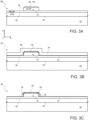
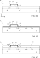
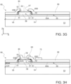
Figure 3A-3H are cross-sections of a semiconductor wafer in subsequent manufacturing steps of the HEMT device ofFigure 2 ; -
Figure 4A-4C are cross-sections of a semiconductor wafer in subsequent manufacturing steps of a different embodiment of the present HEMT device; -
Figure 5 is a cross-section of an HEMT device according to another embodiment; and -
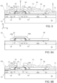
Figures 6A and 6B are cross-sections of a semiconductor wafer in subsequent manufacturing steps the HEMT device ofFigure 5 . - The following description refers to the arrangement shown in the drawings; consequently, expressions such as "above", "below", "upper", "lower", "top", "bottom", "right", "left" and the like are relative to the attached Figures and should not be interpreted in a limiting way.
-
Figure 2 shows aHEMT device 50, comprising asemiconductor body 52, here formed by asubstrate layer 53, achannel layer 54 andbarrier layer 56. -
Substrate layer 53 may comprise a silicon substrate and gallium nitride (GaN) buffer layer, not shown separately inFigure 2 . -
Channel layer 54 is of a first semiconductor material, such as a first semiconductive alloy of elements of the groups III and V of the periodic table; for example,channel layer 54 may be of gallium nitride (GaN). -
Barrier layer 56 overlies, and is in direct contact with,channel layer 54, and is of a second semiconductor material, such as a second semiconductive alloy, different from the first semiconductive alloy, of elements of the groups III-V of the periodic table. For example,barrier layer 56 may be of aluminium gallium nitride (AlGaN). -
Channel layer 54 andbarrier layer 56 are for example of N-type. - A
gate region 57, of conductive material, extends on and in contact withbarrier layer 56. In a manner not shown,gate region 57 is strip-shaped and extends along a first horizontal axis Y of a cartesian reference system XYZ. - In
Figure 2 ,gate region 57 comprises achannel modulating region 58, here of pGaN (gallium nitride of P conductivity type), and aninterlayer region 59. - As known to the person skilled in the art,
channel modulating region 58 operates to modulate the thickness of the channel formed at the interface between thechannel layer 56 and thebarrier layer 56, based on the voltage applied thereto. -
Interlayer region 59 operates to facilitate switching-on ofchannel modulating region 58 and to create a barrier to the diffusion of contaminants of upper layers, as described later on.Interlayer region 59 may be of a material such as TiN. - In the embodiment of
Figure 2 ,interlayer region 59 has a smaller width thanchannel modulating region 58, along a second horizontal axis X of cartesian reference system XYZ.Interlayer region 59 is optional. -
Sealing regions 61 cover lateral sides and (partially) an upper side ofchannel modulating region 58 as well as lateral sides ofinterlayer region 59 and extend along the first horizontal axis Y.Sealing regions 61 are formed by a layer a non-conductive material, for example an oxide such as Al2O3. As alternatives, HfO2, AlN and AlON may be used. - Sealing
regions 61 may have a thickness comprised between 2 and 10 nm, for example of 2.5 nm. -
Spacer regions 62 extend laterally and contiguously to the sealingregions 61, on both sides ofchannel modulating region 58 and ofinterlayer region 59.Spacer regions 62 are of a dielectric material such as silicon oxide. - A
passivation layer 65 extends on the sides of thespacer regions 62 and on thesubstrate 52. In detail,passivation layer 65 has twosurface portions 65A (each extending on and in contact withbarrier layer 56 on opposite sides of gate region 57) and two raisedportions 65B extending each on arespective spacer region 62 and, partially, on a respective side ofinterlayer region 59. - The
surface portions 65A ofpassivation layer 65, extending onbarrier layer 56, form an access region ofHEMT device 50. -
Passivation layer 65 is opened oninterlayer region 59 to expose most of the upper surface of the latter.Passivation layer 65 is of an insulating material, e.g., AlN. - In general,
passivation layer 65 may have a thickness different from the thickness of the sealingregions 61. - In this embodiment,
passivation layer 65 has a greater thickness than the layer forming the sealingregions 61. In particular,passivation layer 65 may have a thickness comprised between 2 and 10 nm, for example of 5 nm. - A first insulating
layer 66, for example of silicon oxide, extends onpassivation layer 65 and is opened on theinterlayer region 59, thereby forming, together withpassivation layer 65, agate opening 67. - A
gate metal 68, for example a multilayer of TiN/AlCu/TiN, extends in thegate opening 67, in direct electrical contact with theinterlayer region 59, and partially on the first insulatinglayer 66. - A second insulating
layer 69, for example of silicon oxide, extends on first insulatinglayer 66 and ongate metal 68. - First and second insulating
layers structure structure source opening 82 and adrain opening 83, extending on different sides ofgate region 57, through the entire thickness of insulatingstructure barrier layer 56. - A
source metal region 72, for example of Ti/AlCu/TiN, extends in source opening 82 and is here in direct electrical contact withbarrier layer 56. InHEMT device 50,source metal region 72 has a portion extending also over thegate metal 68 and over thefield plate 70 and has a shielding function. - A
field plate 70 may extend on the first insulatinglayer 66, on a side, but at a distance ofgate region 57, below the second insulatinglayer 69.Field plate 70 is possibly formed from a same metal layer asgate metal 68 and is electrically connected to sourcemetal region 72. - A
drain metal region 73, for example of Ti/AlCu/TiN, extends indrain opening 83 and is here in direct electrical contact withbarrier layer 56.Drain metal region 73 is on an opposite side ofgate region 57 with respect to sourcemetal region 72. -
HEMT device 50 ofFigure 2 , by having the sealingregions 61 on the sides ofgate region 57 that have different properties from thesurface portions 65A at the access region, forms different 2DEGs at the gate region and at the access region and, namely, a first 2DEG (hereinafter also called gate 2DEG) at the interface between thechannel layer 54 and thebarrier layer 56 undergate region 57 and a second 2DEG (hereinafter also called access 2DEG) at the interface between thechannel layer 54 and thebarrier layer 56 under thesurface portions 65A ofpassivation layer 65. - By tailoring and optimizing the parameters/features of the sealing
regions 61 and thepassivation layer 65, it is thus possible to tailor and optimize the densities of gate 2DEG and of access 2DEG according to the desired properties. - In particular, with the structure of
Figure 2 , it is possible to have a high sheet resistance Rsh under and aroundgate region 57, resulting in a high threshold voltage and low electric field at the corner betweenchannel modulating region 58 and barrier layer 56 (at gate 2DEG) and a low sheet resistance Rsh underpassivation layer 65, resulting in a low on-resistance Ron (at access 2DEG). -
HEMT device 50 thus allows to obtain a good trade-off between gate current, threshold voltage and on-resistance. -
HEMT device 50 may be manufactured as shown inFigures 3A-3H , showing a wafer before dicing and using the same reference numbers as the homonymous regions inFigure 2 . -
Figure 3A shows awafer 80 comprising a stack of layers includingsubstrate layer 53,channel layer 54 andbarrier layer 56.Gate region 57 has been already formed onbarrier layer 56. - For example,
channel modulating region 58 andinterlayer region 59 may be formed by sputtering a TiN layer on a pGaN layer (not shown, grown epitaxially on barrier layer 56) and by lithographically defining the TiN layer and the pGaN layer using a single mask (also not shown) with a lateral etch to obtain the smaller width ofinterlayer region 59; however any other manufacturing steps are possible, for example by using two different masks. - In
Figure 3B , asealing layer 61 is formed ongate region 57 and onbarrier layer 56, where exposed, and then anoxide layer 81 is formed. - For example, sealing
layer 61 is thermally or plasma deposited with an ALD (Atomic Layer Deposition) technique in a H2O or O3 based environment at 300°C for a thickness of, e.g., 2.5 nm. -
Oxide layer 81 may be, e.g., deposited by PECVD (Plasma Enhanced Chemical Vapour Deposition) in a SiO2 SiH4-based environment for a thickness of, e.g., 200 nm. - In
Figure 3C ,oxide layer 81 is anisotropically (dry) etched, without mask, to remove it from the surface ofbarrier layer 56 and from the top ofinterlayer region 59 and leaving it on the lateral surface ofgate region 57, thereby formingspacer regions 62. - In
Figure 3D , sealinglayer 61 is etched on top ofinterlayer region 59 and overbarrier layer 56, where not covered byspacer regions 62. For example, etching is a wet one, done using an etchant selective with respect to the material ofbarrier layer 56 of AlGaN, in particular using EKC265™ produced by DuPont™. Thereby, a selective removal frombarrier layer 56 can be obtained, without damaging thebarrier layer 56 itself, and thus, in operation, without affecting access 2DEG. As a consequence, the sheet resistance Rsh is not negatively affected by this etching. - A surface portion of the
sealing layer 61 also remains under thespacers 62. - In
Figure 3E ,passivation layer 65 is formed, e.g. of AlN and using an ALD technique at about 370°C for a thickness of, for example, 5 nm. - In
Figure 3F , first insulatinglayer 66, for example of silicon oxide, is deposited, for example by PECVD in a SiO2 SiH4-based environment for a thickness of, e.g., 50 nm. - In
Figure 3G ,first insulation layer 66 andpassivation layer 65 are etched using a mask (not shown) to formgate opening 67, thereby exposing the top surface ofgate region 57. Etching offirst insulation layer 66 andpassivation layer 65 may be a time etch, of wet or dry etch, depending on selectivity of the used material, as known to the person skilled in the art. - In
Figure 3H , a gate metal layer is deposited and defined to form gate metal 68 (in gate opening 67) and field plate 70 (laterally thereto). Gate metal layer may be a multilayer of TiN/AlCu/TiN. - Then, in a manner not shown, second insulating
layer 69 is deposited and then defined together with first insulation layer 66 (using a mask not shown) to form source opening 82 anddrain opening 83. Thereafter a source/drain metal layer is deposited and defined to formsource metal region 72 and drainmetal region 73. - Then final manufacturing steps follow, including depositing an outer passivation layer, opening contacts and dicing the
wafer 80, thereby obtainingHEMT device 50 ofFigure 2 . -
Figures 4A-4C relate to a different embodiment, including a double-level field plate. - In particular,
Figure 4A showswafer 80 after the step ofFigure 3F . Here, before opening first insulatinglayer 66 andpassivation layer 65, astep forming region 85 is formed. For example, a SiN layer is deposited and defined. Step formingregion 85 extends here laterally togate region 57, on the side thereof facingdrain metal region 73. - In
Figure 4B ,first insulation layer 66 andpassivation layer 65 are etched to formgate opening 67 and to expose the top surface ofgate region 57, analogously to what described above with reference toFigure 3G . - In
Figure 4C , gate metal layer is deposited and defined to form gate metal 68 (in gate opening 67) and field plate 70'. Here, field plate 70' extends partially over thefirst insulation layer 66 and partially on thestep forming region 85 and thus is not planar. - Then, the second insulating
layer 69 is deposited and etched; the source and drainmetal region -
Figure 5 shows anHEMT device 100 wherein the source and the drain metal regions are formed before the gate metal region. - In detail, in
Figure 5 , where regions common toHEMT device 50 ofFigure 2 have been indicated using the same reference numbers, source and the drain metal regions (here indicated by 72', 73') are formed only through thefirst insulation layer 66 and gate metal region (here indicated by 68') is formed after forming thesecond insulation layer 69, through both insulation layers 66, 69. - In detail, as shown in
Figure 6A , after forming the first insulation layer 66 (Figure 3F ), the latter is defined to form source opening, here indicated by 82' and drain opening, here indicated by 83'.Passivation layer 65 is also removed from thebody 52, at the source opening 82' and drain opening 83'. - Then, source metal region 72', drain metal region 73' and
field plate 70 are formed, by depositing and defining a same metal layer or stack, for example of Ti/AlCu/TiN. - Thereafter,
Figure 6B ,second insulation layer 69 is deposited and etched (together withfirst insulation layer 66 and passivation layer 65) to form gate opening, here indicated by 67'. Thus, inFigures 6B and 5 , gate opening 67' extends through both the first and the second insulation layers 66, 69. - Gate metal, here indicated by 68', is then formed, by depositing and defining a metal layer or stack, for example Ti/AlCu/TiN; in this step, a shielding
region 86 may be formed from the same metal layer of gate metal 68'. -
Shielding region 86 may be electrically coupled other regions in thesubstrate 52 by forming one or more vias through first and second insulation layers 66, 69, in a position not shown inFigure 5 . - Then, final manufacturing steps follow, as described above.
- Finally, it is clear that numerous variations and modifications may be made to the HEMT device and process described and illustrated herein, all falling within the scope of the invention, as defined in the attached claims.
- In general,
passivation layer 65 may have same or greater thickness than the sealingregions 61. - Summarizing, example embodiments of the present disclosure are the following.
- Example 1. A HEMT device (50; 100) comprising:
- a semiconductor body (52) having a semiconductive heterostructure (54, 56);
- a gate region (57), comprising a semiconductor material, arranged on the semiconductor body (52), the gate region having lateral sides;
- sealing regions (61) of non-conductive material, extending on and in contact with the lateral sides of the gate region (57); and
- a passivation layer (65) of non-conductive material, the passivation layer having surface portions (65A) extending on the semiconductor body (52), laterally and at a distance from the lateral sides of the gate region,
- the sealing regions (61) and the passivation layer (65) having different geometrical parameters and/or being of different material.
- Example 1bis. A HEMT device according to example 1, wherein gate region (57) is arranged in direct contact with the semiconductor body (52).
- Example 1ter. A HEMT device according to example 1 or 1bis, wherein the surface portions (65A) of the passivation layer (65) are arranged on and in direct contact with the semiconductor body (52).
- Example 2. A HEMT device according to example 1, 1bis or 1ter, further comprising:
- an insulating structure (66, 69) extending above the semiconductor body (52), laterally and on top of the gate region;
- a first current conducting terminal (72; 72'), of conductive material, extending on and in contact with the semiconductor body (52) laterally to one of the lateral sides of the gate region (57), at least partially through the insulating structure (66, 69);
- a second current conducting terminal (73; 73'), of conductive material, extending on and in contact with the semiconductor body (52) laterally to another of the lateral sides of the gate region (57), at least partially through the insulating structure (66, 69); and
- a control terminal (68; 68'), of conductive material, extending on and in contact with the gate region (57), at least partially through the insulating structure (66, 69).
- Example 3. A HEMT device according to any of the preceding examples, wherein the sealing regions (61) are of an insulating material, such as Al2O3, HfO2, AlN and AlON.
- Example 4. A HEMT device according to any of the preceding examples, wherein the sealing regions (61) have a thickness comprised between 2 and 10 nm, for example of 2.5 nm.
- Example 5. A HEMT device according to any of the preceding examples, wherein the passivation layer (65) is of an insulating material, such as AlN.
- Example 6. A HEMT device according to any of the preceding examples, wherein the passivation layer (65) has a thickness comprised between 2 and 10 nm, for example of 5 nm.
- Example 7. A HEMT device according to any of the preceding examples, wherein the passivation layer (65) has a greater thickness than the sealing regions (61).
- Example 8. A HEMT device according to any of the preceding examples, further comprising spacer regions (62), of dielectric material, extending laterally and in contact with the sealing regions (61), the passivation layer (65) having raised portions (65B) extending on the spacer regions (62), laterally and at a distance from the sealing regions.
- Example 9. A process for manufacturing a HEMT device (50; 100), the process comprising:
- on a semiconductor body (52) having a semiconductive heterostructure (54, 56), forming a gate region (57), the gate region including a semiconductor material and arranged on the semiconductor body (52), the gate region having lateral sides;
- forming sealing regions (61), of non-conductive material, on and in contact with the lateral sides of the gate region (57); and
- forming a passivation layer (65) of non-conductive material, the passivation layer having surface portions (65A) extending on the semiconductor body (52), laterally and at a distance from the lateral sides of the gate region,
- the sealing regions (61) and the passivation layer (65) having different geometrical parameters and/or being of different material.
- Example 10. A process according to the preceding example, wherein forming sealing regions (61) comprises:
- forming, on the gate region (57) and on the semiconductor body (52), a sealing layer (61);
- forming, on the sealing layer and adjacent to the gate region, spacer regions (62); and
- selectively removing the sealing layer (61) on the semiconductor body (52), where exposed.
- Example 10bis. A process according to the preceding example, wherein selectively removing the sealing layer (61) includes removing the sealing layer (61) on top of the gate region (57).
- Example 11. A process according to example 10 or 10bis, wherein selectively removing the sealing layer (61) comprises using an etchant selective with respect to the semiconductor body (52).
- Example 12. A process according to example 10 or 11, wherein forming a passivation layer (65) comprises:
- depositing the passivation layer (65) on the semiconductor body (52), on the spacer regions (62) and on a top surface of the gate region (57); and
- selectively removing the passivation layer (65) from the top surface of the gate region.
- Example 13. A process according to the preceding example, wherein selectively removing the passivation layer (65) comprises:
- forming a first insulating layer (66) on the passivation layer (65);
- forming a control opening (67) in the first insulating layer (66), above the gate region (57); and
- removing the passivation layer (65) in the control opening (67);
- the process further comprising:
- forming a control terminal (68) of conductive material on the gate region, the control terminal extending in the control opening (67);
- forming a second insulating layer (69) on the first insulating layer (66) and on the control terminal (68);
- forming a first conduction opening (82) and a second conduction opening (83) through the first and second insulating layers (66, 69), laterally to the sealing regions (61); and
- forming a first and second current conducting terminal (72, 73) of conductive material on and in contact with the semiconductor body (52) in the first and, respectively, the second conduction openings (82, 83).
- Example 14. A process according to example 12, the process further comprising:
- forming a first insulating layer (66) on the passivation layer (65);
- forming a first conduction opening (82') and a second conduction opening (83') through the first insulating layer (66), laterally to the sealing regions (61);
- forming a first and second current conducting terminals (72', 73') of conductive material on and in contact with the semiconductor body (52) in the first and, respectively, the second conduction openings (82', 83');
- forming a second insulating layer (69) on the first insulating layer (66) and on the first and second current conducting terminals (72', 73');
- forming a control opening (67') through the first and second insulating layers (66, 69), above the gate region (57), wherein forming a control opening (67') comprises said selectively removing the passivation layer (65); and
- forming a control terminal (68') of conductive material on the gate region (57), the control terminal extending in the control opening (67').
- Example 15. A process according to any of examples 9-14, wherein the sealing regions (61) are of a first insulating material, such as Al2O3, HfO2, AlN and AlON, and the passivation layer (65) is of a second insulating material, such as AlN.
- Example 16. A process according to any of examples 9-14, wherein the sealing regions (61) and the passivation layer (65) have different thicknesses.
Claims (15)
- A HEMT device (50; 100) comprising:a semiconductor body (52) having a semiconductive heterostructure (54, 56);a gate region (57), comprising a semiconductor material, arranged on the semiconductor body (52), the gate region having lateral sides;sealing regions (61) of non-conductive material, extending on and in contact with the lateral sides of the gate region (57);a passivation layer (65) of non-conductive material, the passivation layer having surface portions (65A) extending on the semiconductor body (52), laterally and at a distance from the lateral sides of the gate region; andspacer regions (62), extending laterally and in contact with the sealing regions (61), the passivation layer (65) furthermore having raised portions (65B) extending on the spacer regions (62), laterally and at a distance from the sealing regions (61),the sealing regions (61) and the passivation layer (65) having different thicknesses and/or being of different material.
- A HEMT device according to claim 1, further comprising:an insulating structure (66, 69) extending above the semiconductor body (52), laterally and on top of the gate region;a first current conducting terminal (72; 72'), of conductive material, extending on and in contact with the semiconductor body (52) laterally to one of the lateral sides of the gate region (57), at least partially through the insulating structure (66, 69);a second current conducting terminal (73; 73'), of conductive material, extending on and in contact with the semiconductor body (52) laterally to another of the lateral sides of the gate region (57), at least partially through the insulating structure (66, 69); anda control terminal (68; 68'), of conductive material, extending on and in contact with the gate region (57), at least partially through the insulating structure (66, 69).
- A HEMT device according to claim 1 or 2, wherein the sealing regions (61) are of an insulating material, such as Al2O3, HfO2, AlN and AlON.
- A HEMT device according to any of the preceding claims, wherein the sealing regions (61) have a thickness comprised between 2 and 10 nm, for example of 2.5 nm.
- A HEMT device according to any of the preceding claims, wherein the passivation layer (65) is of an insulating material, such as AlN.
- A HEMT device according to any of the preceding claims, wherein the passivation layer (65) has a thickness comprised between 2 and 10 nm, for example of 5 nm.
- A HEMT device according to any of the preceding claims, wherein the passivation layer (65) has a greater thickness than the sealing regions (61).
- A HEMT device according to any of the preceding claims, wherein the spacer regions (62) are of a dielectric material, such as silicon oxide.
- A process for manufacturing a HEMT device (50; 100), the process comprising:on a semiconductor body (52) having a semiconductive heterostructure (54, 56), forming a gate region (57), the gate region including a semiconductor material and arranged on the semiconductor body (52), the gate region having lateral sides;forming sealing regions (61), of non-conductive material, on and in contact with the lateral sides of the gate region (57);forming spacer regions (62), laterally and in contact with the sealing regions (61); andforming a passivation layer (65) of non-conductive material, the passivation layer having surface portions (65A) extending on the semiconductor body (52), laterally and at a distance from the lateral sides of the gate region, the passivation layer (65) furthermore having raised portions (65B) extending on the spacer regions (62), laterally and at a distance from the sealing regions (61),the sealing regions (61) and the passivation layer (65) having different thicknesses and/or being of different material.
- A process according to the preceding claim, wherein forming sealing regions (61) comprises:before forming the spacer regions (62), forming, on the gate region (57) and on the semiconductor body (52), a sealing layer (61); andafter forming the spacer regions (62), selectively removing the sealing layer (61) on the semiconductor body (52), where exposed,wherein forming the spacer regions (62) comprises forming the spacer regions (62) on the sealing layer and adjacent to the gate region.
- A process according to the preceding claim, wherein selectively removing the sealing layer (61) comprises using an etchant selective with respect to the semiconductor body (52).
- A process according to claim 10 or 11, wherein forming a passivation layer (65) comprises:depositing the passivation layer (65) on the semiconductor body (52), on the spacer regions (62) and on a top surface of the gate region (57); andselectively removing the passivation layer (65) from the top surface of the gate region.
- A process according to the preceding claim, wherein selectively removing the passivation layer (65) comprises:forming a first insulating layer (66) on the passivation layer (65);forming a control opening (67) in the first insulating layer (66), above the gate region (57); andremoving the passivation layer (65) in the control opening (67) ;the process further comprising:forming a control terminal (68) of conductive material on the gate region, the control terminal extending in the control opening (67);forming a second insulating layer (69) on the first insulating layer (66) and on the control terminal (68);forming a first conduction opening (82) and a second conduction opening (83) through the first and second insulating layers (66, 69), laterally to the sealing regions (61); andforming a first and second current conducting terminal (72, 73) of conductive material on and in contact with the semiconductor body (52) in the first and, respectively, the second conduction openings (82, 83).
- A process according to claim 12, the process further comprising:forming a first insulating layer (66) on the passivation layer (65);forming a first conduction opening (82') and a second conduction opening (83') through the first insulating layer (66), laterally to the sealing regions (61);forming a first and second current conducting terminals (72', 73') of conductive material on and in contact with the semiconductor body (52) in the first and, respectively, the second conduction openings (82', 83');forming a second insulating layer (69) on the first insulating layer (66) and on the first and second current conducting terminals (72', 73');forming a control opening (67') through the first and second insulating layers (66, 69), above the gate region (57), wherein forming a control opening (67') comprises said selectively removing the passivation layer (65); andforming a control terminal (68') of conductive material on the gate region (57), the control terminal extending in the control opening (67').
- A process according to any of claims 9-14, wherein the sealing regions (61) are of a first insulating material, such as Al2O3, HfO2, AlN and AlON, and the passivation layer (65) is of a second insulating material, such as AlN.
Applications Claiming Priority (1)
| Application Number | Priority Date | Filing Date | Title |
|---|---|---|---|
| IT102023000004566A IT202300004566A1 (en) | 2023-03-10 | 2023-03-10 | HEMT DEVICE WITH REDUCED IGNITION RESISTANCE AND RELATED MANUFACTURING PROCEDURE |
Publications (1)
| Publication Number | Publication Date |
|---|---|
| EP4428928A1 true EP4428928A1 (en) | 2024-09-11 |
Family
ID=86332036
Family Applications (1)
| Application Number | Title | Priority Date | Filing Date |
|---|---|---|---|
| EP24305307.1A Pending EP4428928A1 (en) | 2023-03-10 | 2024-02-27 | Hemt device having a reduced on-resistance and manufacturing process thereof |
Country Status (3)
| Country | Link |
|---|---|
| US (1) | US20240304711A1 (en) |
| EP (1) | EP4428928A1 (en) |
| IT (1) | IT202300004566A1 (en) |
Citations (2)
| Publication number | Priority date | Publication date | Assignee | Title |
|---|---|---|---|---|
| US20130193485A1 (en) | 2012-01-27 | 2013-08-01 | Fujitsu Semiconductor Limited | Compound semiconductor device and method of manufacturing the same |
| US20200335617A1 (en) | 2019-04-18 | 2020-10-22 | Semiconductor Components Industries, Llc | Electronic Device Including a High Electron Mobility Transistor Including a Gate Electrode and a Dielectric Film |
-
2023
- 2023-03-10 IT IT102023000004566A patent/IT202300004566A1/en unknown
-
2024
- 2024-02-27 EP EP24305307.1A patent/EP4428928A1/en active Pending
- 2024-03-01 US US18/592,816 patent/US20240304711A1/en active Pending
Patent Citations (2)
| Publication number | Priority date | Publication date | Assignee | Title |
|---|---|---|---|---|
| US20130193485A1 (en) | 2012-01-27 | 2013-08-01 | Fujitsu Semiconductor Limited | Compound semiconductor device and method of manufacturing the same |
| US20200335617A1 (en) | 2019-04-18 | 2020-10-22 | Semiconductor Components Industries, Llc | Electronic Device Including a High Electron Mobility Transistor Including a Gate Electrode and a Dielectric Film |
Also Published As
| Publication number | Publication date |
|---|---|
| IT202300004566A1 (en) | 2024-09-10 |
| US20240304711A1 (en) | 2024-09-12 |
Similar Documents
| Publication | Publication Date | Title |
|---|---|---|
| EP3734666B1 (en) | Semiconductor device and fabrication method thereof | |
| CN111834452B (en) | Electronic devices | |
| US8530937B2 (en) | Compound semiconductor device having insulation film with different film thicknesses beneath electrodes | |
| US10872967B2 (en) | Manufacturing method of semiconductor device | |
| US7750369B2 (en) | Nitride semiconductor device | |
| KR20240008373A (en) | Methods for manufacturing high electron mobility transistors with improved performance | |
| US20190115443A1 (en) | Gate stack for heterostructure device | |
| CN114068682B (en) | Symmetrical arrangement of field plates in semiconductor devices | |
| CN114930509B (en) | Semiconductor device and method for manufacturing the same | |
| US10243049B2 (en) | Nitride semiconductor device | |
| JP2022145319A (en) | Semiconductor device | |
| EP4120364A1 (en) | Semiconductor device and manufacturing method thereof | |
| EP4428930A1 (en) | Hemt device having improved on-state performance and manufacturing process thereof | |
| US9087888B2 (en) | Semiconductor device and electronic apparatus | |
| JP7844306B2 (en) | Semiconductor equipment | |
| US20240304711A1 (en) | Hemt device having a reduced on-resistance and manufacturing process thereof | |
| US20230317840A1 (en) | Hemt and method of fabricating the same | |
| CN114975573B (en) | High electron mobility transistor and manufacturing method thereof | |
| CN222339881U (en) | HEMT device | |
| EP4428929A1 (en) | Hemt device having a reduced gate leakage and manufacturing process thereof | |
| CN222582862U (en) | HEMT Devices | |
| CN222547914U (en) | Semiconductor devices and HEMT devices | |
| CN118630052A (en) | HEMT device with reduced on-resistance and manufacturing process thereof | |
| EP4471869A1 (en) | Hemt device having an improved conductivity and manufacturing process thereof | |
| US20240194763A1 (en) | Hemt transistor |
Legal Events
| Date | Code | Title | Description |
|---|---|---|---|
| PUAI | Public reference made under article 153(3) epc to a published international application that has entered the european phase |
Free format text: ORIGINAL CODE: 0009012 |
|
| STAA | Information on the status of an ep patent application or granted ep patent |
Free format text: STATUS: THE APPLICATION HAS BEEN PUBLISHED |
|
| AK | Designated contracting states |
Kind code of ref document: A1 Designated state(s): AL AT BE BG CH CY CZ DE DK EE ES FI FR GB GR HR HU IE IS IT LI LT LU LV MC ME MK MT NL NO PL PT RO RS SE SI SK SM TR |
|
| STAA | Information on the status of an ep patent application or granted ep patent |
Free format text: STATUS: REQUEST FOR EXAMINATION WAS MADE |
|
| 17P | Request for examination filed |
Effective date: 20250310 |