EP4428924A1 - High performance silicon controlled rectifier devices - Google Patents
High performance silicon controlled rectifier devices Download PDFInfo
- Publication number
- EP4428924A1 EP4428924A1 EP24152505.4A EP24152505A EP4428924A1 EP 4428924 A1 EP4428924 A1 EP 4428924A1 EP 24152505 A EP24152505 A EP 24152505A EP 4428924 A1 EP4428924 A1 EP 4428924A1
- Authority
- EP
- European Patent Office
- Prior art keywords
- well
- trench isolation
- deep
- semiconductor substrate
- deep trench
- Prior art date
- Legal status (The legal status is an assumption and is not a legal conclusion. Google has not performed a legal analysis and makes no representation as to the accuracy of the status listed.)
- Pending
Links
- XUIMIQQOPSSXEZ-UHFFFAOYSA-N Silicon Chemical compound [Si] XUIMIQQOPSSXEZ-UHFFFAOYSA-N 0.000 title abstract description 9
- 229910052710 silicon Inorganic materials 0.000 title abstract description 9
- 239000010703 silicon Substances 0.000 title abstract description 9
- 238000002955 isolation Methods 0.000 claims abstract description 95
- 239000004065 semiconductor Substances 0.000 claims abstract description 59
- 239000000758 substrate Substances 0.000 claims abstract description 46
- 238000000034 method Methods 0.000 claims abstract description 31
- 239000000463 material Substances 0.000 claims abstract description 25
- 238000009792 diffusion process Methods 0.000 claims description 46
- 229910021332 silicide Inorganic materials 0.000 claims description 15
- FVBUAEGBCNSCDD-UHFFFAOYSA-N silicide(4-) Chemical compound [Si-4] FVBUAEGBCNSCDD-UHFFFAOYSA-N 0.000 claims description 15
- 230000000903 blocking effect Effects 0.000 claims description 8
- 238000004519 manufacturing process Methods 0.000 abstract description 15
- 238000000151 deposition Methods 0.000 description 8
- 238000002513 implantation Methods 0.000 description 7
- 230000008021 deposition Effects 0.000 description 6
- 239000002019 doping agent Substances 0.000 description 6
- 229910052723 transition metal Inorganic materials 0.000 description 6
- 150000003624 transition metals Chemical class 0.000 description 6
- 238000005530 etching Methods 0.000 description 5
- 150000002500 ions Chemical class 0.000 description 5
- PXHVJJICTQNCMI-UHFFFAOYSA-N Nickel Chemical compound [Ni] PXHVJJICTQNCMI-UHFFFAOYSA-N 0.000 description 4
- 230000015556 catabolic process Effects 0.000 description 4
- 238000005516 engineering process Methods 0.000 description 4
- 235000012431 wafers Nutrition 0.000 description 4
- 239000010408 film Substances 0.000 description 3
- 238000001459 lithography Methods 0.000 description 3
- 238000001020 plasma etching Methods 0.000 description 3
- 239000000126 substance Substances 0.000 description 3
- VYPSYNLAJGMNEJ-UHFFFAOYSA-N Silicium dioxide Chemical compound O=[Si]=O VYPSYNLAJGMNEJ-UHFFFAOYSA-N 0.000 description 2
- RTAQQCXQSZGOHL-UHFFFAOYSA-N Titanium Chemical compound [Ti] RTAQQCXQSZGOHL-UHFFFAOYSA-N 0.000 description 2
- 239000000956 alloy Substances 0.000 description 2
- 230000015572 biosynthetic process Effects 0.000 description 2
- 238000003486 chemical etching Methods 0.000 description 2
- 239000007795 chemical reaction product Substances 0.000 description 2
- 238000005229 chemical vapour deposition Methods 0.000 description 2
- 229910017052 cobalt Inorganic materials 0.000 description 2
- 239000010941 cobalt Substances 0.000 description 2
- GUTLYIVDDKVIGB-UHFFFAOYSA-N cobalt atom Chemical compound [Co] GUTLYIVDDKVIGB-UHFFFAOYSA-N 0.000 description 2
- 230000001419 dependent effect Effects 0.000 description 2
- 239000003989 dielectric material Substances 0.000 description 2
- 238000005468 ion implantation Methods 0.000 description 2
- 229910052751 metal Inorganic materials 0.000 description 2
- 239000002184 metal Substances 0.000 description 2
- 229910001092 metal group alloy Inorganic materials 0.000 description 2
- 229910052759 nickel Inorganic materials 0.000 description 2
- 150000004767 nitrides Chemical class 0.000 description 2
- 229920002120 photoresistant polymer Polymers 0.000 description 2
- 238000005498 polishing Methods 0.000 description 2
- 239000000047 product Substances 0.000 description 2
- 239000010936 titanium Substances 0.000 description 2
- 229910052719 titanium Inorganic materials 0.000 description 2
- 229910021350 transition metal silicide Inorganic materials 0.000 description 2
- ZOXJGFHDIHLPTG-UHFFFAOYSA-N Boron Chemical compound [B] ZOXJGFHDIHLPTG-UHFFFAOYSA-N 0.000 description 1
- 229910001218 Gallium arsenide Inorganic materials 0.000 description 1
- 229910000673 Indium arsenide Inorganic materials 0.000 description 1
- OAICVXFJPJFONN-UHFFFAOYSA-N Phosphorus Chemical compound [P] OAICVXFJPJFONN-UHFFFAOYSA-N 0.000 description 1
- 229910003811 SiGeC Inorganic materials 0.000 description 1
- 229910000577 Silicon-germanium Inorganic materials 0.000 description 1
- ATJFFYVFTNAWJD-UHFFFAOYSA-N Tin Chemical compound [Sn] ATJFFYVFTNAWJD-UHFFFAOYSA-N 0.000 description 1
- 238000000137 annealing Methods 0.000 description 1
- 229910052787 antimony Inorganic materials 0.000 description 1
- WATWJIUSRGPENY-UHFFFAOYSA-N antimony atom Chemical compound [Sb] WATWJIUSRGPENY-UHFFFAOYSA-N 0.000 description 1
- 229910052785 arsenic Inorganic materials 0.000 description 1
- RQNWIZPPADIBDY-UHFFFAOYSA-N arsenic atom Chemical compound [As] RQNWIZPPADIBDY-UHFFFAOYSA-N 0.000 description 1
- 238000004380 ashing Methods 0.000 description 1
- QVGXLLKOCUKJST-UHFFFAOYSA-N atomic oxygen Chemical compound [O] QVGXLLKOCUKJST-UHFFFAOYSA-N 0.000 description 1
- 229910052796 boron Inorganic materials 0.000 description 1
- 239000000969 carrier Substances 0.000 description 1
- 239000000919 ceramic Substances 0.000 description 1
- 229910052681 coesite Inorganic materials 0.000 description 1
- 150000001875 compounds Chemical class 0.000 description 1
- 239000000356 contaminant Substances 0.000 description 1
- 229910052906 cristobalite Inorganic materials 0.000 description 1
- 229910021419 crystalline silicon Inorganic materials 0.000 description 1
- 238000005137 deposition process Methods 0.000 description 1
- -1 e.g. Substances 0.000 description 1
- 238000003384 imaging method Methods 0.000 description 1
- RPQDHPTXJYYUPQ-UHFFFAOYSA-N indium arsenide Chemical compound [In]#[As] RPQDHPTXJYYUPQ-UHFFFAOYSA-N 0.000 description 1
- 239000012212 insulator Substances 0.000 description 1
- 239000013067 intermediate product Substances 0.000 description 1
- 238000012986 modification Methods 0.000 description 1
- 230000004048 modification Effects 0.000 description 1
- 229910003465 moissanite Inorganic materials 0.000 description 1
- 229910052760 oxygen Inorganic materials 0.000 description 1
- 239000001301 oxygen Substances 0.000 description 1
- 229910052698 phosphorus Inorganic materials 0.000 description 1
- 239000011574 phosphorus Substances 0.000 description 1
- 238000012545 processing Methods 0.000 description 1
- 229910010271 silicon carbide Inorganic materials 0.000 description 1
- 239000000377 silicon dioxide Substances 0.000 description 1
- 238000004528 spin coating Methods 0.000 description 1
- 229910052682 stishovite Inorganic materials 0.000 description 1
- 239000010409 thin film Substances 0.000 description 1
- 238000012546 transfer Methods 0.000 description 1
- 229910052905 tridymite Inorganic materials 0.000 description 1
- WFKWXMTUELFFGS-UHFFFAOYSA-N tungsten Chemical compound [W] WFKWXMTUELFFGS-UHFFFAOYSA-N 0.000 description 1
- 229910052721 tungsten Inorganic materials 0.000 description 1
- 239000010937 tungsten Substances 0.000 description 1
Images




Classifications
-
- H—ELECTRICITY
- H10—SEMICONDUCTOR DEVICES; ELECTRIC SOLID-STATE DEVICES NOT OTHERWISE PROVIDED FOR
- H10D—INORGANIC ELECTRIC SEMICONDUCTOR DEVICES
- H10D62/00—Semiconductor bodies, or regions thereof, of devices having potential barriers
- H10D62/10—Shapes, relative sizes or dispositions of the regions of the semiconductor bodies; Shapes of the semiconductor bodies
- H10D62/113—Isolations within a component, i.e. internal isolations
- H10D62/115—Dielectric isolations, e.g. air gaps
-
- H—ELECTRICITY
- H10—SEMICONDUCTOR DEVICES; ELECTRIC SOLID-STATE DEVICES NOT OTHERWISE PROVIDED FOR
- H10D—INORGANIC ELECTRIC SEMICONDUCTOR DEVICES
- H10D89/00—Aspects of integrated devices not covered by groups H10D84/00 - H10D88/00
- H10D89/60—Integrated devices comprising arrangements for electrical or thermal protection, e.g. protection circuits against electrostatic discharge [ESD]
- H10D89/601—Integrated devices comprising arrangements for electrical or thermal protection, e.g. protection circuits against electrostatic discharge [ESD] for devices having insulated gate electrodes, e.g. for IGFETs or IGBTs
- H10D89/711—Integrated devices comprising arrangements for electrical or thermal protection, e.g. protection circuits against electrostatic discharge [ESD] for devices having insulated gate electrodes, e.g. for IGFETs or IGBTs using bipolar transistors as protective elements
- H10D89/713—Integrated devices comprising arrangements for electrical or thermal protection, e.g. protection circuits against electrostatic discharge [ESD] for devices having insulated gate electrodes, e.g. for IGFETs or IGBTs using bipolar transistors as protective elements including a PNP transistor and a NPN transistor, wherein each of said transistors has its base region coupled to the collector region of the other transistor, e.g. silicon controlled rectifier [SCR] devices
-
- H—ELECTRICITY
- H10—SEMICONDUCTOR DEVICES; ELECTRIC SOLID-STATE DEVICES NOT OTHERWISE PROVIDED FOR
- H10D—INORGANIC ELECTRIC SEMICONDUCTOR DEVICES
- H10D8/00—Diodes
- H10D8/01—Manufacture or treatment
- H10D8/041—Manufacture or treatment of multilayer diodes
-
- H—ELECTRICITY
- H10—SEMICONDUCTOR DEVICES; ELECTRIC SOLID-STATE DEVICES NOT OTHERWISE PROVIDED FOR
- H10D—INORGANIC ELECTRIC SEMICONDUCTOR DEVICES
- H10D8/00—Diodes
- H10D8/80—PNPN diodes, e.g. Shockley diodes or break-over diodes
Definitions
- the present disclosure relates to semiconductor structures and, more particularly, to high performance silicon controlled rectifier (SCR) devices and methods of manufacture.
- SCR silicon controlled rectifier
- a silicon controlled rectifier is a solid-state current-controlling device, which is a unidirectional device (i.e., can conduct current only in one direction).
- the SCR typically includes a switching configuration comprising p-n-p-n layers.
- a holding current of an SCR can be defined as the smallest amount of current under which an anode current has to drop to enter an OFF status. This means if the holding current value is 5 mA, for example, subsequently the SCR's anodes' current has to turn into less than 5 mA to discontinue performing.
- a triggering voltage may occur when the anode terminal is made +ve relating to the cathode in which case the SCR will be in a forwarding biased mode, e.g., enters into the forward blocking state. This means the device is switched from the blocked (OFF) state to the unblocked (ON) state.
- a structure comprises: a first well in a semiconductor substrate; a second well in the semiconductor substrate, adjacent to the first well; a plurality of shallow trench isolation structures extending into the first well and the second well; and a deep trench isolation structure between the plurality of shallow trench isolation structures and extending into the semiconductor material deeper than the plurality of shallow trench isolation structures. Additional features of the structure are set forth in dependent claims 2 to 9.
- a structure comprises: a p-well in a semiconductor substrate; an n-well in the semiconductor substrate and abutting the p-well; first diffusion regions in the n-well connecting to an anode; second diffusion regions in the p-well and connecting to a cathode; shallow trench isolation structures extending into the n-well and the p-well; and a deep trench isolation structure between the shallow trench isolation structures and which is deeper than the shallow trench isolation structures. Additional features of the structure are set forth in dependent claims 11 to 14.
- a method comprises: forming a first well in a semiconductor substrate; forming a second well in the semiconductor substrate, adjacent to the first well; forming a plurality of shallow trench isolation structures extending into the first well and the second well; and forming a deep trench isolation structure between the plurality of shallow trench isolation structures and extending into the semiconductor material deeper than the plurality of shallow trench isolation structures.
- the present disclosure relates to semiconductor structures and, more particularly, to high performance silicon controlled rectifier (SCR) devices and methods of manufacture.
- the SCR devices include a deep trench isolation structure extending into a well, e.g., N-well, P-well or junction of the N/P wells, within semiconductor material, e.g., silicon.
- the SCR devices are high holding SCR devices which exhibit a lower trigger voltage compared to conventional SCR devices.
- the high current performance is due to a deeper current path resulting from the use of the deep trench isolation structure.
- the use of the deep trench isolation structure effectively provides a smaller footprint compared to conventional SCR devices.
- the SCR device includes a first terminal in a first well and a second terminal in a second well adjacent to the first well.
- the first well abuts the second well along an interface or junction.
- the first terminal may be an anode and the second terminal may be a cathode.
- a deep trench isolation structure is provided in one of the wells and, more preferably, at the junction of the first well and the second well.
- the deep trench isolation structure separates the anode from the cathode and will allow the current to be pushed deeper into the semiconductor substrate to block current and increase the high holding voltage.
- the SCR device further comprises shallow trench isolation structures between the first terminal and the second terminal, with the deep trench isolation structure being deeper than the shallow trench isolation structures.
- the SCR devices of the present disclosure can be manufactured in a number of ways using a number of different tools.
- the methodologies and tools are used to form structures with dimensions in the micrometer and nanometer scale.
- the methodologies, i.e., technologies, employed to manufacture the SCR devices of the present disclosure have been adopted from integrated circuit (IC) technology.
- the structures are built on wafers and are realized in films of material patterned by photolithographic processes on the top of a wafer.
- the fabrication of the SCR devices uses three basic building blocks: (i) deposition of thin films of material on a substrate, (ii) applying a patterned mask on top of the films by photolithographic imaging, and (iii) etching the films selectively to the mask.
- precleaning processes may be used to clean etched surfaces of any contaminants, as is known in the art.
- rapid thermal anneal processes may be used to drive-in dopants or material layers as is known in the art.
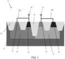
- FIG. 1 shows an SCR device with a deep trench isolation structure and respective fabrication processes in accordance with aspects of the present disclosure.
- the structure 10 of FIG. 1 includes a semiconductor substrate 12 composed of any suitable material including, but not limited to, Si, SiGe, SiGeC, SiC, GaAs, InAs, InP, and other III/V or II/VI compound semiconductors.
- the semiconductor substrate 12 may be a lightly doped p-type semiconductor substrate.
- the semiconductor substrate 12 may be a lightly doped p-type, single crystalline Si substrate with any suitable crystallographic orientation (e.g., a (100), (110), (111), or (001) crystallographic orientation).
- the semiconductor substrate 12 may include wells 14, 16.
- the well 14 may be an N-well and the well 16 may be a P-well.
- the wells 14, 16 are abutting.
- the wells 14, 16 may be formed by introducing different dopant types into the semiconductor substrate 12 by, for example, ion implantation processes.
- a deep trench isolation structure 18 may be provided at the interface or junction of the wells 14, 16.
- the deep trench isolation structure 18 may extend laterally into both the wells 14, 16, extending from a top surface of the semiconductor substrate 12.
- the deep trench isolation structure 18 may extend completely through the wells 14, 16 and into the underlying semiconductor substrate 12. It is also contemplated that other depths of the deep trench isolation structure can be implemented in the present disclosure depending on the desired breakdown voltage. Accordingly, the depth of the deep trench isolation structure 18 may be adjusted to different depths at the interface or junction of the wells 14, 16, depending on required device characteristics.
- shallow trench isolation structures 20 may be provided within the semiconductor substrate 12.
- the shallow trench isolation structures 20 extend vertically into the wells 14, 16 and isolate diffusion regions 22, 24.
- the diffusion regions 22 are N+ diffusion regions and the diffusion regions 24 are P+ diffusion regions, each of which vertically extend into the semiconductor substrate 12 and, more specifically, within the wells 14, 16.
- the shallow trench isolation structures 20 are not as deep as the deep trench isolation structure 18.
- FIG. 1 also representatively shows contacts and/or wiring structures 26a to an anode 28 and contacts and/or wiring structures 26b to a cathode 30.
- the anode 28 is electrically connected to the diffusion regions 22, 24 of the N-well 14 and the cathode 30 is connected to the diffusion regions 22, 24 of the P-well 16.
- the contacts and/or wiring structures 26a, 26b may electrically connect to silicide contacts on the diffusion regions 22, 24.
- the silicide contacts may be formed by a silicide process which begins with deposition of a thin transition metal layer, e.g., nickel, cobalt or titanium, over fully formed and patterned semiconductor devices (e.g., doped or ion implanted diffusion regions). After deposition of the material, the structure is heated allowing the transition metal to react with exposed silicon (or other semiconductor material as described herein) in the active regions of the semiconductor device (e.g., doped or ion implanted diffusion regions) forming a low-resistance transition metal silicide. Following the reaction, any remaining transition metal is removed by chemical etching, leaving silicide contacts in the active regions of the device.
- a thin transition metal layer e.g., nickel, cobalt or titanium
- semiconductor devices e.g., doped or ion implanted diffusion regions
- FIG. 2 shows another SCR device with a deep trench isolation structure.
- the deep trench isolation structure 18 may extend completely within the well 16.
- a diffusion region 24a may be provided at the junction of the wells 14, 16 to provide low and mid voltage breakdown voltage characteristics.
- the deep trench isolation structure 18 isolates the diffusion region 24a and 22.
- the diffusion region 24a is a P+ diffusion region and, as in the previous embodiment, the well 16 may be P-well.
- a silicide blocking material 34 may be formed over the diffusion region 24a (and deep trench isolation structure) to prevent silicide formation.
- the silicide blocking material 34 may extend over the surface of the semiconductor substrate 12 and shallow trench isolation structures 20 (excluding locations which electrically connect to the contacts 26a, 26b for an anode and cathode).
- the depth of the deep trench isolation structure 18 may be adjusted to a depth with the wells or below the wells into the semiconductor substrate 12 for adjustments to the holding voltage.
- the breakdown voltage may be determined by the floating P+/NW junction. The remaining features are similar to the structure 10 of FIG. 1 .
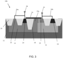
- FIG. 3 shows yet another SCR device with a deep trench isolation structure.
- the deep trench isolation structure 18 may extend completely within the well 14, e.g., N-well.
- a diffusion region 22a may be provided at the junction of the wells 14, 16 to provide low and mid voltage breakdown voltage characteristics.
- the silicide blocking material 34 e.g., nitride or oxide, may be formed over the diffusion region 24a (and deep trench isolation structure) to prevent silicide formation.
- the deep trench isolation structure 18 isolates the diffusion region 24 and 22a.
- the diffusion region 22a is an N+ diffusion region. The remaining features are similar to the structure 10b of FIG. 2 .
- FIG. 4 shows an SCR device with the deep trench isolation structure of FIG. 1 in a deep N-well 32.
- the deep N-well 32 is provided within the semiconductor substrate 12, which isolates the SCR device.
- the wells 14, 16 and deep trench isolation structure 18 sit within the deep N-well 32, which isolates the SCR from other devices.
- the deep N-well 32 may be formed by a conventional ion implantation process as is known in the art and described herein.
- the remaining features of the structure 10b are similar to the structure 10 of FIG. 1 .
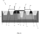
- FIG. 5 shows an SCR device with the deep trench isolation structure of FIG. 2 in a deep N-well 32.
- the deep N-well 32 is provided within the semiconductor substrate 12, which isolates the SCR device.
- the wells 14, 16 and deep trench isolation structure 18 sit within the deep N-well 32 to isolate the SCR from other devices.
- the remaining features of the structure 10d are similar to the structure 10a of FIG. 2 .
- FIG. 6 shows an SCR device with the deep trench isolation structure of FIG. 3 in a deep N-well 32.
- the deep N-well 32 is provided within the semiconductor substrate 12, which again is used to isolate the SCR device.
- the wells 14, 16 and deep trench isolation structure 18 sit within the deep N-well 32.
- the remaining features of the structure 10e are similar to the structure 10b of FIG. 3 .
- the deep trench isolation structure 18 will provide a higher resistance for carriers, and will exhibit a lower capacitance than the semiconductor substrate 12.
- the deep trench isolation structure 18 will allow the current to be pushed deeper into the semiconductor substrate 12 than conventional structures to block current and increase the high holding voltage.
- FIGS. 7A-7C show fabrication processes for manufacturing the SCR device of FIG. 1 . Similar processes can be used to fabricate the devices of FIGS. 2-6 .
- the shallow trench isolation structures 20 are formed within the semiconductor substrate 12.
- the shallow trench isolation structures 20 may be positioned to extend within wells 14, 16 and isolate diffusion regions 22, 24, each of which are formed in later fabrication processes as shown in FIG. 7C .
- the shallow trench isolation structures 20 can be formed by conventional lithography, etching and deposition methods known to those of skill in the art.
- a resist formed over the semiconductor substrate 12 is developed to form a pattern (opening).
- An etching process with a selective chemistry e.g., reactive ion etching (RIE)
- RIE reactive ion etching
- insulator material e.g., SiO 2
- CVD chemical vapor deposition
- Any residual material on the surface of the semiconductor material 12 can be removed by conventional chemical mechanical polishing (CMP) processes.
- the deep trench isolation structure 18 is formed within the semiconductor substrate 12.
- the deep trench isolation structure 18 can be formed by conventional lithography, etching and deposition methods known to those of skill in the art.
- the deep trench isolation structure 189 can be fabricated prior to the fabrication of the shallow trench isolation structures 20.
- the deep trench isolation structure 18 will extend into the semiconductor substrate 12 deeper than the shallow trench isolation structures 20.
- the deep trench isolation structure 18 can be formed to align with either well 14, 16 or a junction between the wells as shown in FIGS. 1-4 .
- the deep trench isolation structure 18 may extend to different depths, any of which would be deeper than the shallow trench isolation structures 20.
- FIG. 7C shows the fabrication processes of forming the wells 14, 16 and diffusion regions 22, 24 (and also diffusion regions 22a, 24a).
- the wells 14, 16 and diffusion regions 22, 24 may be formed by introducing a concentration of a different dopant of opposite conductivity type in the semiconductor substrate.
- the wells 14, 16 will abut one another; whereas the diffusion regions 22, 24 will be provided between the shallow trench isolation structures 20 and within the wells 14, 16.
- respective patterned implantation masks may be used to define selected areas exposed for the implantations of the wells 14, 16 and diffusion regions 22, 24.
- the implantation mask used to select the exposed area for forming a well and/or diffusion regions is stripped after implantation, and before the implantation mask used to form another well or diffusion region of different conductivity type.
- the implantation masks may include a layer of a light-sensitive material, such as an organic photoresist, applied by a spin coating process, pre-baked, exposed to light projected through a photomask, baked after exposure, and developed with a chemical developer.
- Each of the implantation masks has a thickness and stopping power sufficient to block masked areas against receiving a dose of the implanted ions.
- the P-well 16 and p-diffusion regions 24 may be doped with different concentrations of p-type dopants, e.g., Boron (B), and the N-well 14 and n-diffusion regions 22 may be doped with different concentrations of n-type dopants, e.g., Arsenic (As), Phosphorus (P) and Antimony (Sb), among other suitable examples.
- An annealing process may be performed to drive in the dopant into the semiconductor substrate 12.
- the contacts and/or wiring structures 26a, 26b may be formed by conventional back end of the line (BEOL) processes.
- BEOL back end of the line
- an interlevel dielectric material may be deposited over the semiconductor substrate 12, which is then subjected to lithography and etching processes (e.g., RIE), followed by deposition of metal or metal alloy material, e.g., tungsten with a TaN or TiN liner. Any residual metal or metal alloy material on the interlevel dielectric material may be removed by a conventional chemical mechanical polishing (CMP) process.
- CMP chemical mechanical polishing
- the silicide process begins with deposition of a thin transition metal layer, e.g., nickel, cobalt or titanium, over fully formed and patterned semiconductor devices (e.g., doped or ion implanted diffusion regions). After deposition of the material, the structure is heated allowing the transition metal to react with exposed silicon (or other semiconductor material as described herein) in the active regions of the semiconductor device (e.g., doped or ion implanted diffusion regions) forming a low-resistance transition metal silicide. Following the reaction, any remaining transition metal is removed by chemical etching, leaving silicide contacts in the active regions of the device.
- a thin transition metal layer e.g., nickel, cobalt or titanium
- semiconductor devices e.g., doped or ion implanted diffusion regions
- the SCR devices can be utilized in system on chip (SoC) technology.
- SoC is an integrated circuit (also known as a "chip") that integrates all components of an electronic system on a single chip or substrate. As the components are integrated on a single substrate, SoCs consume much less power and take up much less area than multichip designs with equivalent functionality. Because of this, SoCs are becoming the dominant force in the mobile computing (such as in Smartphones) and edge computing markets. SoC is also used in embedded systems and the Internet of Things.
- the method(s) as described above is used in the fabrication of integrated circuit chips.
- the resulting integrated circuit chips can be distributed by the fabricator in raw wafer form (that is, as a single wafer that has multiple unpackaged chips), as a bare die, or in a packaged form.
- the chip is mounted in a single chip package (such as a plastic carrier, with leads that are affixed to a motherboard or other higher level carrier) or in a multichip package (such as a ceramic carrier that has either or both surface interconnections or buried interconnections).
- the chip is then integrated with other chips, discrete circuit elements, and/or other signal processing devices as part of either (a) an intermediate product, such as a motherboard, or (b) an end product.
- the end product can be any product that includes integrated circuit chips, ranging from toys and other low-end applications to advanced computer products having a display, a keyboard or other input device, and a central processor.
Landscapes
- Element Separation (AREA)
Abstract
The present disclosure relates to semiconductor structures and, more particularly, to high performance silicon controlled rectifier (SCR) devices and methods of manufacture. The structure includes: a first well in a semiconductor substrate; a second well in the semiconductor substrate, adjacent to the first well; a plurality of shallow trench isolation structures extending into the first well and the second well; and a deep trench isolation structure between the plurality of shallow trench isolation structures and extending into the semiconductor material deeper than the plurality of shallow trench isolation structures.
Description
- The present disclosure relates to semiconductor structures and, more particularly, to high performance silicon controlled rectifier (SCR) devices and methods of manufacture.
- A silicon controlled rectifier (SCR) is a solid-state current-controlling device, which is a unidirectional device (i.e., can conduct current only in one direction). The SCR typically includes a switching configuration comprising p-n-p-n layers.
- A holding current of an SCR can be defined as the smallest amount of current under which an anode current has to drop to enter an OFF status. This means if the holding current value is 5 mA, for example, subsequently the SCR's anodes' current has to turn into less than 5 mA to discontinue performing. A triggering voltage, on the other hand, may occur when the anode terminal is made +ve relating to the cathode in which case the SCR will be in a forwarding biased mode, e.g., enters into the forward blocking state. This means the device is switched from the blocked (OFF) state to the unblocked (ON) state.
- In an aspect of the disclosure, a structure comprises: a first well in a semiconductor substrate; a second well in the semiconductor substrate, adjacent to the first well; a plurality of shallow trench isolation structures extending into the first well and the second well; and a deep trench isolation structure between the plurality of shallow trench isolation structures and extending into the semiconductor material deeper than the plurality of shallow trench isolation structures. Additional features of the structure are set forth in dependent claims 2 to 9.
- In an aspect of the disclosure, a structure comprises: a p-well in a semiconductor substrate; an n-well in the semiconductor substrate and abutting the p-well; first diffusion regions in the n-well connecting to an anode; second diffusion regions in the p-well and connecting to a cathode; shallow trench isolation structures extending into the n-well and the p-well; and a deep trench isolation structure between the shallow trench isolation structures and which is deeper than the shallow trench isolation structures. Additional features of the structure are set forth in dependent claims 11 to 14.
- In an aspect of the disclosure, a method comprises: forming a first well in a semiconductor substrate; forming a second well in the semiconductor substrate, adjacent to the first well; forming a plurality of shallow trench isolation structures extending into the first well and the second well; and forming a deep trench isolation structure between the plurality of shallow trench isolation structures and extending into the semiconductor material deeper than the plurality of shallow trench isolation structures.
- The present disclosure is described in the detailed description which follows, in reference to the noted plurality of drawings by way of non-limiting examples of exemplary embodiments of the present disclosure.
-
FIG. 1 shows a silicon controlled rectifier (SCR) device with a deep trench isolation structure and respective fabrication processes in accordance with aspects of the present disclosure. -
FIG. 2 shows an SCR device with a deep trench isolation structure in a P-well in accordance with additional aspects of the present disclosure. -
FIG. 3 shows an SCR device with a deep trench isolation structure in an N-well in accordance with additional aspects of the present disclosure. -
FIG. 4 shows an SCR device with the deep trench isolation structure ofFIG. 1 in a deep N-well in accordance with aspects of the present disclosure. -
FIG. 5 shows an SCR device with the deep trench isolation structure ofFIG. 2 in a deep N-well in accordance with aspects of the present disclosure. -
FIG. 6 shows an SCR device with the deep trench isolation structure ofFIG. 3 in a deep N-well in accordance with aspects of the present disclosure. -
FIGS. 7A-7C show fabrication processes for manufacturing the SCR device ofFIG. 1 in accordance with aspects of the present disclosure. - The present disclosure relates to semiconductor structures and, more particularly, to high performance silicon controlled rectifier (SCR) devices and methods of manufacture. In embodiments, the SCR devices include a deep trench isolation structure extending into a well, e.g., N-well, P-well or junction of the N/P wells, within semiconductor material, e.g., silicon. Advantageously, in these configurations, the SCR devices are high holding SCR devices which exhibit a lower trigger voltage compared to conventional SCR devices. For example, the high current performance is due to a deeper current path resulting from the use of the deep trench isolation structure. Moreover, the use of the deep trench isolation structure effectively provides a smaller footprint compared to conventional SCR devices.
- In more specific embodiments, the SCR device includes a first terminal in a first well and a second terminal in a second well adjacent to the first well. The first well abuts the second well along an interface or junction. The first terminal may be an anode and the second terminal may be a cathode. A deep trench isolation structure is provided in one of the wells and, more preferably, at the junction of the first well and the second well. In embodiments, the deep trench isolation structure separates the anode from the cathode and will allow the current to be pushed deeper into the semiconductor substrate to block current and increase the high holding voltage. The SCR device further comprises shallow trench isolation structures between the first terminal and the second terminal, with the deep trench isolation structure being deeper than the shallow trench isolation structures.
- The SCR devices of the present disclosure can be manufactured in a number of ways using a number of different tools. In general, though, the methodologies and tools are used to form structures with dimensions in the micrometer and nanometer scale. The methodologies, i.e., technologies, employed to manufacture the SCR devices of the present disclosure have been adopted from integrated circuit (IC) technology. For example, the structures are built on wafers and are realized in films of material patterned by photolithographic processes on the top of a wafer. In particular, the fabrication of the SCR devices uses three basic building blocks: (i) deposition of thin films of material on a substrate, (ii) applying a patterned mask on top of the films by photolithographic imaging, and (iii) etching the films selectively to the mask. In addition, precleaning processes may be used to clean etched surfaces of any contaminants, as is known in the art. Moreover, when necessary, rapid thermal anneal processes may be used to drive-in dopants or material layers as is known in the art.
-
FIG. 1 shows an SCR device with a deep trench isolation structure and respective fabrication processes in accordance with aspects of the present disclosure. In particular, thestructure 10 ofFIG. 1 includes asemiconductor substrate 12 composed of any suitable material including, but not limited to, Si, SiGe, SiGeC, SiC, GaAs, InAs, InP, and other III/V or II/VI compound semiconductors. Thesemiconductor substrate 12 may be a lightly doped p-type semiconductor substrate. In more specific embodiments, thesemiconductor substrate 12 may be a lightly doped p-type, single crystalline Si substrate with any suitable crystallographic orientation (e.g., a (100), (110), (111), or (001) crystallographic orientation). - The
semiconductor substrate 12 may includewells wells FIG. 7C , thewells semiconductor substrate 12 by, for example, ion implantation processes. - A deep
trench isolation structure 18 may be provided at the interface or junction of thewells trench isolation structure 18 may extend laterally into both thewells semiconductor substrate 12. In embodiments, the deeptrench isolation structure 18 may extend completely through thewells underlying semiconductor substrate 12. It is also contemplated that other depths of the deep trench isolation structure can be implemented in the present disclosure depending on the desired breakdown voltage. Accordingly, the depth of the deeptrench isolation structure 18 may be adjusted to different depths at the interface or junction of thewells - Still referring to
FIG. 1 , shallowtrench isolation structures 20 may be provided within thesemiconductor substrate 12. In embodiments, the shallowtrench isolation structures 20 extend vertically into thewells isolate diffusion regions diffusion regions 22 are N+ diffusion regions and thediffusion regions 24 are P+ diffusion regions, each of which vertically extend into thesemiconductor substrate 12 and, more specifically, within thewells trench isolation structures 20 are not as deep as the deeptrench isolation structure 18. -
FIG. 1 also representatively shows contacts and/orwiring structures 26a to ananode 28 and contacts and/orwiring structures 26b to acathode 30. In embodiments, theanode 28 is electrically connected to thediffusion regions well 14 and thecathode 30 is connected to thediffusion regions well 16. The contacts and/orwiring structures diffusion regions - As should be understood by those of skill in the art, the silicide contacts may be formed by a silicide process which begins with deposition of a thin transition metal layer, e.g., nickel, cobalt or titanium, over fully formed and patterned semiconductor devices (e.g., doped or ion implanted diffusion regions). After deposition of the material, the structure is heated allowing the transition metal to react with exposed silicon (or other semiconductor material as described herein) in the active regions of the semiconductor device (e.g., doped or ion implanted diffusion regions) forming a low-resistance transition metal silicide. Following the reaction, any remaining transition metal is removed by chemical etching, leaving silicide contacts in the active regions of the device.
-
FIG. 2 shows another SCR device with a deep trench isolation structure. In thestructure 10a ofFIG. 2 , the deeptrench isolation structure 18 may extend completely within thewell 16. In addition, adiffusion region 24a may be provided at the junction of thewells trench isolation structure 18 isolates thediffusion region diffusion region 24a is a P+ diffusion region and, as in the previous embodiment, the well 16 may be P-well. - Still referring to
FIG. 2 , asilicide blocking material 34, e.g., nitride or oxide, may be formed over thediffusion region 24a (and deep trench isolation structure) to prevent silicide formation. As in any of the embodiments, thesilicide blocking material 34 may extend over the surface of thesemiconductor substrate 12 and shallow trench isolation structures 20 (excluding locations which electrically connect to thecontacts trench isolation structure 18 may be adjusted to a depth with the wells or below the wells into thesemiconductor substrate 12 for adjustments to the holding voltage. Also, the breakdown voltage may be determined by the floating P+/NW junction. The remaining features are similar to thestructure 10 ofFIG. 1 . -
FIG. 3 shows yet another SCR device with a deep trench isolation structure. In thestructure 10b ofFIG. 3 , the deeptrench isolation structure 18 may extend completely within the well 14, e.g., N-well. In addition, adiffusion region 22a may be provided at the junction of thewells silicide blocking material 34, e.g., nitride or oxide, may be formed over thediffusion region 24a (and deep trench isolation structure) to prevent silicide formation. In embodiments, the deeptrench isolation structure 18 isolates thediffusion region diffusion region 22a is an N+ diffusion region. The remaining features are similar to thestructure 10b ofFIG. 2 . -
FIG. 4 shows an SCR device with the deep trench isolation structure ofFIG. 1 in a deep N-well 32. In thestructure 10c ofFIG. 4 , the deep N-well 32 is provided within thesemiconductor substrate 12, which isolates the SCR device. In more specific embodiments, thewells trench isolation structure 18 sit within the deep N-well 32, which isolates the SCR from other devices. The deep N-well 32 may be formed by a conventional ion implantation process as is known in the art and described herein. The remaining features of thestructure 10b are similar to thestructure 10 ofFIG. 1 . -
FIG. 5 shows an SCR device with the deep trench isolation structure ofFIG. 2 in a deep N-well 32. In thestructure 10d ofFIG. 5 , the deep N-well 32 is provided within thesemiconductor substrate 12, which isolates the SCR device. In more specific embodiments, thewells trench isolation structure 18 sit within the deep N-well 32 to isolate the SCR from other devices. The remaining features of thestructure 10d are similar to thestructure 10a ofFIG. 2 . -
FIG. 6 shows an SCR device with the deep trench isolation structure ofFIG. 3 in a deep N-well 32. In thestructure 10e ofFIG. 6 , the deep N-well 32 is provided within thesemiconductor substrate 12, which again is used to isolate the SCR device. In more specific embodiments, thewells trench isolation structure 18 sit within the deep N-well 32. The remaining features of thestructure 10e are similar to thestructure 10b ofFIG. 3 . - In each of the embodiments, the deep
trench isolation structure 18 will provide a higher resistance for carriers, and will exhibit a lower capacitance than thesemiconductor substrate 12. The deeptrench isolation structure 18 will allow the current to be pushed deeper into thesemiconductor substrate 12 than conventional structures to block current and increase the high holding voltage. -
FIGS. 7A-7C show fabrication processes for manufacturing the SCR device ofFIG. 1 . Similar processes can be used to fabricate the devices ofFIGS. 2-6 . InFIG. 7A , for example, the shallowtrench isolation structures 20 are formed within thesemiconductor substrate 12. In embodiments, the shallowtrench isolation structures 20 may be positioned to extend withinwells diffusion regions FIG. 7C . - The shallow
trench isolation structures 20 can be formed by conventional lithography, etching and deposition methods known to those of skill in the art. For example, a resist formed over thesemiconductor substrate 12 is developed to form a pattern (opening). An etching process with a selective chemistry, e.g., reactive ion etching (RIE), will be used to transfer the pattern from the patterned photoresist layer to thesemiconductor substrate 12. Following the resist removal by a conventional oxygen ashing process or other known stripants, insulator material (e.g., SiO2) can be deposited by any conventional deposition processes, e.g., chemical vapor deposition (CVD) processes within the respective trenches. Any residual material on the surface of thesemiconductor material 12 can be removed by conventional chemical mechanical polishing (CMP) processes. - In
FIG. 7B , the deeptrench isolation structure 18 is formed within thesemiconductor substrate 12. As with the shallowtrench isolation structures 20, the deeptrench isolation structure 18 can be formed by conventional lithography, etching and deposition methods known to those of skill in the art. In embodiments, the deep trench isolation structure 189 can be fabricated prior to the fabrication of the shallowtrench isolation structures 20. - The deep
trench isolation structure 18 will extend into thesemiconductor substrate 12 deeper than the shallowtrench isolation structures 20. The deeptrench isolation structure 18 can be formed to align with either well 14, 16 or a junction between the wells as shown inFIGS. 1-4 . In addition, depending on the desired performance characteristics, the deeptrench isolation structure 18 may extend to different depths, any of which would be deeper than the shallowtrench isolation structures 20. -
FIG. 7C shows the fabrication processes of forming thewells diffusion regions 22, 24 (and alsodiffusion regions wells diffusion regions wells diffusion regions trench isolation structures 20 and within thewells - In embodiments, respective patterned implantation masks may be used to define selected areas exposed for the implantations of the
wells diffusion regions diffusion regions 24 may be doped with different concentrations of p-type dopants, e.g., Boron (B), and the N-well 14 and n-diffusion regions 22 may be doped with different concentrations of n-type dopants, e.g., Arsenic (As), Phosphorus (P) and Antimony (Sb), among other suitable examples. An annealing process may be performed to drive in the dopant into thesemiconductor substrate 12. - Referring back to
FIG. 1 , the contacts and/orwiring structures semiconductor substrate 12, which is then subjected to lithography and etching processes (e.g., RIE), followed by deposition of metal or metal alloy material, e.g., tungsten with a TaN or TiN liner. Any residual metal or metal alloy material on the interlevel dielectric material may be removed by a conventional chemical mechanical polishing (CMP) process. - As should be understood by those of skill in the art, the silicide process begins with deposition of a thin transition metal layer, e.g., nickel, cobalt or titanium, over fully formed and patterned semiconductor devices (e.g., doped or ion implanted diffusion regions). After deposition of the material, the structure is heated allowing the transition metal to react with exposed silicon (or other semiconductor material as described herein) in the active regions of the semiconductor device (e.g., doped or ion implanted diffusion regions) forming a low-resistance transition metal silicide. Following the reaction, any remaining transition metal is removed by chemical etching, leaving silicide contacts in the active regions of the device.
- The SCR devices can be utilized in system on chip (SoC) technology. The SoC is an integrated circuit (also known as a "chip") that integrates all components of an electronic system on a single chip or substrate. As the components are integrated on a single substrate, SoCs consume much less power and take up much less area than multichip designs with equivalent functionality. Because of this, SoCs are becoming the dominant force in the mobile computing (such as in Smartphones) and edge computing markets. SoC is also used in embedded systems and the Internet of Things.
- The method(s) as described above is used in the fabrication of integrated circuit chips. The resulting integrated circuit chips can be distributed by the fabricator in raw wafer form (that is, as a single wafer that has multiple unpackaged chips), as a bare die, or in a packaged form. In the latter case the chip is mounted in a single chip package (such as a plastic carrier, with leads that are affixed to a motherboard or other higher level carrier) or in a multichip package (such as a ceramic carrier that has either or both surface interconnections or buried interconnections). In any case the chip is then integrated with other chips, discrete circuit elements, and/or other signal processing devices as part of either (a) an intermediate product, such as a motherboard, or (b) an end product. The end product can be any product that includes integrated circuit chips, ranging from toys and other low-end applications to advanced computer products having a display, a keyboard or other input device, and a central processor.
- The descriptions of the various embodiments of the present disclosure have been presented for purposes of illustration, but are not intended to be exhaustive or limited to the embodiments disclosed. Many modifications and variations will be apparent to those of ordinary skill in the art without departing from the scope and spirit of the described embodiments. The terminology used herein was chosen to best explain the principles of the embodiments, the practical application or technical improvement over technologies found in the marketplace, or to enable others of ordinary skill in the art to understand the embodiments disclosed herein.
Claims (15)
- A structure comprising:a first well in a semiconductor substrate;a second well in the semiconductor substrate, adjacent to the first well;a plurality of shallow trench isolation structures extending into the first well and the second well; anda deep trench isolation structure between the plurality of shallow trench isolation structures and extending into the semiconductor material deeper than the plurality of shallow trench isolation structures.
- The structure of claim 1, wherein the first well comprises an N-well and the second well comprises a P-well.
- The structure of claim 1 or claim 2, further comprising diffusion regions in the first well and the second well, wherein the plurality of shallow trench isolation structures extending into the first well and the second well isolate the diffusion regions.
- The structure of claim 2 or claim 3, wherein the deep trench isolation structure is at an interface between the N-well and the P-well.
- The structure of claim 2 or claim 3, wherein the deep trench isolation structure is within the N-well and an N+ diffusion region extends between a junction of the N-well and the P-well, adjacent to the deep trench isolation structure.
- The structure of claim 5, further comprising a silicide blocking material over the N+ diffusion region.
- The structure of claim 2 or claim 3, wherein the deep trench isolation structure is within the P-well and a P+ diffusion region extends between a junction of the N-well and the P-well, adjacent to the deep trench isolation structure.
- The structure of claim 7, further comprising a silicide blocking material over the P+ diffusion region.
- The structure of one of claims 1 to 8, further comprising a deep N-well within the semiconductor substrate, wherein the first well, the second well and the deep trench isolation structure sit within the deep N-well.
- A structure comprising:a p-well in a semiconductor substrate;an n-well in the semiconductor substrate and abutting the p-well;first diffusion regions in the n-well connecting to an anode;second diffusion regions in the p-well and connecting to a cathode;shallow trench isolation structures extending into the n-well and the p-well;
anda deep trench isolation structure between the shallow trench isolation structures and which is deeper than the shallow trench isolation structures. - The structure of claim 10, wherein the deep trench isolation structure is provided at a junction of the n-well and the p-well.
- The structure of claim 10, further comprising an N+ diffusion extending at a junction of the n-well and the p-well, and the deep trench isolation structure is in the n-well, and, optionally, further comprising a silicide blocking material over the N+ diffusion.
- The structure of claim 10, further comprising a P+ diffusion extending at a junction of the n-well and the p-well, and the deep trench isolation structure is in the p-well, and, optionally, further comprising a silicide blocking material over the P+ diffusion.
- The structure of one of claims 10 to 13, further comprising a deep N-well within the semiconductor substrate, wherein the n-well, the p-well and the deep trench isolation structure sit within the deep N-well.
- A method comprising:forming a first well in a semiconductor substrate;forming a second well in the semiconductor substrate, adjacent to the first well;forming a plurality of shallow trench isolation structures extending into the first well and the second well; andforming a deep trench isolation structure between the plurality of shallow trench isolation structures and extending into the semiconductor material deeper than the plurality of shallow trench isolation structures.
Applications Claiming Priority (1)
| Application Number | Priority Date | Filing Date | Title |
|---|---|---|---|
| US18/118,323 US20240304612A1 (en) | 2023-03-07 | 2023-03-07 | High performance silicon controlled rectifier devices |
Publications (1)
| Publication Number | Publication Date |
|---|---|
| EP4428924A1 true EP4428924A1 (en) | 2024-09-11 |
Family
ID=89661589
Family Applications (1)
| Application Number | Title | Priority Date | Filing Date |
|---|---|---|---|
| EP24152505.4A Pending EP4428924A1 (en) | 2023-03-07 | 2024-01-18 | High performance silicon controlled rectifier devices |
Country Status (3)
| Country | Link |
|---|---|
| US (1) | US20240304612A1 (en) |
| EP (1) | EP4428924A1 (en) |
| CN (1) | CN118630009A (en) |
Citations (2)
| Publication number | Priority date | Publication date | Assignee | Title |
|---|---|---|---|---|
| US20120043583A1 (en) * | 2010-08-20 | 2012-02-23 | International Business Machines Corporation | Low leakage, low capacitance electrostatic discharge (esd) silicon controlled recitifer (scr), methods of manufacture and design structure |
| US20200135715A1 (en) * | 2018-10-26 | 2020-04-30 | Globalfoundries Inc. | Silicon-controlled rectifiers with wells laterally isolated by trench isolation regions |
Family Cites Families (4)
| Publication number | Priority date | Publication date | Assignee | Title |
|---|---|---|---|---|
| CN106876369A (en) * | 2017-03-01 | 2017-06-20 | 中国电子科技集团公司第五十八研究所 | For the silicon controlled rectifier (SCR) and preparation method of thin epitaxy technique electrostatic discharge (ESD) protection |
| US10636869B2 (en) * | 2018-03-09 | 2020-04-28 | Xilinx, Inc. | Mitigation for FinFET technology using deep isolation |
| CN110085573A (en) * | 2019-05-06 | 2019-08-02 | 德淮半导体有限公司 | Electrostatic protection structure, image sensor structure and preparation method |
| US12426362B2 (en) * | 2021-08-04 | 2025-09-23 | Halo Microelectronics International | Latch-up free high voltage device |
-
2023
- 2023-03-07 US US18/118,323 patent/US20240304612A1/en active Pending
-
2024
- 2024-01-08 CN CN202410023930.2A patent/CN118630009A/en active Pending
- 2024-01-18 EP EP24152505.4A patent/EP4428924A1/en active Pending
Patent Citations (2)
| Publication number | Priority date | Publication date | Assignee | Title |
|---|---|---|---|---|
| US20120043583A1 (en) * | 2010-08-20 | 2012-02-23 | International Business Machines Corporation | Low leakage, low capacitance electrostatic discharge (esd) silicon controlled recitifer (scr), methods of manufacture and design structure |
| US20200135715A1 (en) * | 2018-10-26 | 2020-04-30 | Globalfoundries Inc. | Silicon-controlled rectifiers with wells laterally isolated by trench isolation regions |
Non-Patent Citations (1)
| Title |
|---|
| BOSELLI C ET AL: "Latch-up in 65nm CMOS technology: a scaling perspective", RELIABILITY PHYSICS SYMPOSIUM, 2005. PROCEEDINGS. 43RD ANNUAL. 2005 IE EE INTERNATIONAL SAN JOSE, CA, USA APRIL 17-21, 2005, PISCATAWAY, NJ, USA,IEEE, 17 April 2005 (2005-04-17), pages 137 - 144, XP010826888, ISBN: 978-0-7803-8803-1, DOI: 10.1109/RELPHY.2005.1493075 * |
Also Published As
| Publication number | Publication date |
|---|---|
| US20240304612A1 (en) | 2024-09-12 |
| CN118630009A (en) | 2024-09-10 |
Similar Documents
| Publication | Publication Date | Title |
|---|---|---|
| US8017471B2 (en) | Structure and method of latchup robustness with placement of through wafer via within CMOS circuitry | |
| EP4203068A1 (en) | Bipolar transistors | |
| US11978733B2 (en) | High-voltage electrostatic discharge devices | |
| EP4340026A1 (en) | Trigger for silicon controlled rectifier | |
| EP4579749A1 (en) | Electrostatic device | |
| US12604532B2 (en) | Silicon controlled rectifiers | |
| EP4456137A1 (en) | Electrostatic discharge devices | |
| EP4401138A2 (en) | Electrostatic device | |
| US20240304612A1 (en) | High performance silicon controlled rectifier devices | |
| EP4421874A1 (en) | High performance silicon controlled rectifier devices | |
| US12550452B2 (en) | Silicon controlled rectifiers | |
| US20240304613A1 (en) | Silicon controlled rectifers with field plate | |
| US20250126817A1 (en) | Silicon controlled rectifiers | |
| US12336302B1 (en) | Vertical device triggered silicon control rectifier | |
| EP4590087A1 (en) | Silicon control rectifiers | |
| EP4604173A2 (en) | Device with improved latch-up immunity | |
| EP4553902A1 (en) | Silicon control rectifier integrated with a transistor | |
| EP4583664A1 (en) | Transistor triggered silicon control rectifier | |
| US20250220940A1 (en) | Device triggered silicon control rectifier | |
| EP4716412A1 (en) | Diode triggered silicon controlled rectifiers | |
| US12324248B2 (en) | Electrostatic discharge device with pinch resistor | |
| EP4567875B1 (en) | Silicon controlled rectifier integrated heterojunction bipolar transistor | |
| US20260143726A1 (en) | Capacitor |
Legal Events
| Date | Code | Title | Description |
|---|---|---|---|
| PUAI | Public reference made under article 153(3) epc to a published international application that has entered the european phase |
Free format text: ORIGINAL CODE: 0009012 |
|
| STAA | Information on the status of an ep patent application or granted ep patent |
Free format text: STATUS: THE APPLICATION HAS BEEN PUBLISHED |
|
| AK | Designated contracting states |
Kind code of ref document: A1 Designated state(s): AL AT BE BG CH CY CZ DE DK EE ES FI FR GB GR HR HU IE IS IT LI LT LU LV MC ME MK MT NL NO PL PT RO RS SE SI SK SM TR |
|
| STAA | Information on the status of an ep patent application or granted ep patent |
Free format text: STATUS: REQUEST FOR EXAMINATION WAS MADE |
|
| 17P | Request for examination filed |
Effective date: 20250207 |