EP4428590A1 - Optical coupler moisture barrier - Google Patents
Optical coupler moisture barrier Download PDFInfo
- Publication number
- EP4428590A1 EP4428590A1 EP24160753.0A EP24160753A EP4428590A1 EP 4428590 A1 EP4428590 A1 EP 4428590A1 EP 24160753 A EP24160753 A EP 24160753A EP 4428590 A1 EP4428590 A1 EP 4428590A1
- Authority
- EP
- European Patent Office
- Prior art keywords
- layers
- optical
- layer
- photonic chip
- stack
- Prior art date
- Legal status (The legal status is an assumption and is not a legal conclusion. Google has not performed a legal analysis and makes no representation as to the accuracy of the status listed.)
- Pending
Links
Images




Classifications
-
- G—PHYSICS
- G02—OPTICS
- G02B—OPTICAL ELEMENTS, SYSTEMS OR APPARATUS
- G02B6/00—Light guides; Structural details of arrangements comprising light guides and other optical elements, e.g. couplings
- G02B6/24—Coupling light guides
- G02B6/42—Coupling light guides with opto-electronic elements
- G02B6/4201—Packages, e.g. shape, construction, internal or external details
- G02B6/4204—Packages, e.g. shape, construction, internal or external details the coupling comprising intermediate optical elements, e.g. lenses, holograms
- G02B6/4212—Packages, e.g. shape, construction, internal or external details the coupling comprising intermediate optical elements, e.g. lenses, holograms the intermediate optical element being a coupling medium interposed therebetween, e.g. epoxy resin, refractive index matching material, index grease, matching liquid or gel
-
- G—PHYSICS
- G02—OPTICS
- G02B—OPTICAL ELEMENTS, SYSTEMS OR APPARATUS
- G02B6/00—Light guides; Structural details of arrangements comprising light guides and other optical elements, e.g. couplings
- G02B6/24—Coupling light guides
- G02B6/26—Optical coupling means
- G02B6/30—Optical coupling means for use between fibre and thin-film device
-
- C—CHEMISTRY; METALLURGY
- C23—COATING METALLIC MATERIAL; COATING MATERIAL WITH METALLIC MATERIAL; CHEMICAL SURFACE TREATMENT; DIFFUSION TREATMENT OF METALLIC MATERIAL; COATING BY VACUUM EVAPORATION, BY SPUTTERING, BY ION IMPLANTATION OR BY CHEMICAL VAPOUR DEPOSITION, IN GENERAL; INHIBITING CORROSION OF METALLIC MATERIAL OR INCRUSTATION IN GENERAL
- C23C—COATING METALLIC MATERIAL; COATING MATERIAL WITH METALLIC MATERIAL; SURFACE TREATMENT OF METALLIC MATERIAL BY DIFFUSION INTO THE SURFACE, BY CHEMICAL CONVERSION OR SUBSTITUTION; COATING BY VACUUM EVAPORATION, BY SPUTTERING, BY ION IMPLANTATION OR BY CHEMICAL VAPOUR DEPOSITION, IN GENERAL
- C23C16/00—Chemical coating by decomposition of gaseous compounds, without leaving reaction products of surface material in the coating, i.e. chemical vapour deposition [CVD] processes
- C23C16/44—Chemical coating by decomposition of gaseous compounds, without leaving reaction products of surface material in the coating, i.e. chemical vapour deposition [CVD] processes characterised by the method of coating
- C23C16/455—Chemical coating by decomposition of gaseous compounds, without leaving reaction products of surface material in the coating, i.e. chemical vapour deposition [CVD] processes characterised by the method of coating characterised by the method used for introducing gases into reaction chamber or for modifying gas flows in reaction chamber
- C23C16/45523—Pulsed gas flow or change of composition over time
- C23C16/45525—Atomic layer deposition [ALD]
-
- G—PHYSICS
- G02—OPTICS
- G02B—OPTICAL ELEMENTS, SYSTEMS OR APPARATUS
- G02B1/00—Optical elements characterised by the material of which they are made; Optical coatings for optical elements
- G02B1/10—Optical coatings produced by application to, or surface treatment of, optical elements
- G02B1/14—Protective coatings, e.g. hard coatings
-
- G—PHYSICS
- G02—OPTICS
- G02B—OPTICAL ELEMENTS, SYSTEMS OR APPARATUS
- G02B6/00—Light guides; Structural details of arrangements comprising light guides and other optical elements, e.g. couplings
- G02B6/10—Light guides; Structural details of arrangements comprising light guides and other optical elements, e.g. couplings of the optical waveguide type
- G02B6/12—Light guides; Structural details of arrangements comprising light guides and other optical elements, e.g. couplings of the optical waveguide type of the integrated circuit kind
- G02B6/13—Integrated optical circuits characterised by the manufacturing method
- G02B6/132—Integrated optical circuits characterised by the manufacturing method by deposition of thin films
-
- G—PHYSICS
- G02—OPTICS
- G02B—OPTICAL ELEMENTS, SYSTEMS OR APPARATUS
- G02B6/00—Light guides; Structural details of arrangements comprising light guides and other optical elements, e.g. couplings
- G02B6/24—Coupling light guides
- G02B6/42—Coupling light guides with opto-electronic elements
- G02B6/4201—Packages, e.g. shape, construction, internal or external details
- G02B6/4204—Packages, e.g. shape, construction, internal or external details the coupling comprising intermediate optical elements, e.g. lenses, holograms
-
- G—PHYSICS
- G02—OPTICS
- G02B—OPTICAL ELEMENTS, SYSTEMS OR APPARATUS
- G02B6/00—Light guides; Structural details of arrangements comprising light guides and other optical elements, e.g. couplings
- G02B6/24—Coupling light guides
- G02B6/42—Coupling light guides with opto-electronic elements
- G02B6/4201—Packages, e.g. shape, construction, internal or external details
- G02B6/4251—Sealed packages
- G02B6/4253—Sealed packages by embedding housing components in an adhesive or a polymer material
-
- H—ELECTRICITY
- H10—SEMICONDUCTOR DEVICES; ELECTRIC SOLID-STATE DEVICES NOT OTHERWISE PROVIDED FOR
- H10H—INORGANIC LIGHT-EMITTING SEMICONDUCTOR DEVICES HAVING POTENTIAL BARRIERS
- H10H20/00—Individual inorganic light-emitting semiconductor devices having potential barriers, e.g. light-emitting diodes [LED]
- H10H20/80—Constructional details
- H10H20/84—Coatings, e.g. passivation layers or antireflective coatings
-
- G—PHYSICS
- G02—OPTICS
- G02B—OPTICAL ELEMENTS, SYSTEMS OR APPARATUS
- G02B6/00—Light guides; Structural details of arrangements comprising light guides and other optical elements, e.g. couplings
- G02B6/24—Coupling light guides
- G02B6/42—Coupling light guides with opto-electronic elements
- G02B6/4201—Packages, e.g. shape, construction, internal or external details
- G02B6/4219—Mechanical fixtures for holding or positioning the elements relative to each other in the couplings; Alignment methods for the elements, e.g. measuring or observing methods especially used therefor
- G02B6/4236—Fixing or mounting methods of the aligned elements
- G02B6/4239—Adhesive bonding; Encapsulation with polymer material
Definitions
- the present invention relates to an optical coupler moisture barrier.
- Photonics products are typically composed of various elements, which may include fibers, photonic chips implementing photonic integrated circuits (PIC), and electronic components, such as drivers and transimpedance amplifiers (TIAs), wire-bonded or flip-chip bonded onto a carrier substrate assembled in one package.
- the package may be hermetically sealed, to protect the products from the environment, but hermeticity comes with tradeoffs, such as manufacturing complications and cost. Depending on the product, sometimes hermeticity is a requirement, and other times non-hermetic packages are an option.
- a desirable feature of packages would be the ability of having non-hermetic packages that can pass some of the qualification tests, such as the damp heat test, which are typically standardized in terms of temperature, humidity and time by Telcordia.
- a PIC is especially sensitive to damp heat, because the encapsulation oxides that are used in standard wafer fabrication are typically deposited at lower temperatures and are of lesser quality (non-stoichiometric) than thermal oxide, and may also be under higher stresses.
- the lower quality oxide will tend to absorb water during damp heat testing, which will change the properties of the oxide, such as stress and refractive index.
- An optical edge coupler of a photonic chip may guide a large and delocalized mode ( ⁇ 10 ⁇ m of diameter), which may significantly overlap with the encapsulation oxide.
- an oxide can absorb water and the resulting refractive index change may impact the properties of optical edge couplers, such as insertion loss and polarization dependent loss.
- the changes in properties can exceed 1 dB in change which is highly undesirable.
- the changes should be no more than 0.5 dB and be resilient to the point that no measurable change is seen under damp heat.
- the use of conventional hermetic packages seals the PIC from the environment, but results in larger and more expensive packages that do not necessarily meet form-factor standards.
- Some embodiments may overcome some of the above-mentioned shortcomings of prior art by utilizing a higher quality deposition process, such as atomic layer deposition (ALD), in order to deposit a moisture barrier comprising a multi-layer stack of dielectric materials, thin enough to be optically compatible with optical couplers integrated on photonic chips.
- ALD atomic layer deposition
- the ALD layers are of high quality and protect the moisture sensitive oxide underneath.
- the present invention relates to an apparatus comprising a photonic a photonic chip comprising an optical edge coupler for end-coupling an external optical waveguide to the photonic chip, the optical edge coupler having one end at an edge of the chip; and a coating on, at least, a part of the edge of the chip over the one end of the optical edge coupler, the coating being a stack interleaving first and second dielectric layers of different material composition, the stack including at least 2 interfaces between adjacent ones of the first and second layers.
- the external optical waveguide may be, e.g., an optical fiber or an optical waveguide of another photonic chip.
- the coating includes at least four of the layers. In some implementations, the coating may have a thickness of 10 to 150 nanometers. In some implementations, the coating may have a thickness of 25 to 100 nanometers.
- each of the layers may be less than 25 nanometers thick.
- the coating may cover at least half of a surface of the photonic chip.
- each second layer may be one of a silicon nitride layer, aluminum oxide layer, and a hafnium oxide layer.
- each first layer may be a silicon oxide layer.
- the coating starts and ends with a silicon oxide layer.
- each second layer may be thinner than each first layer.
- the apparatus may comprise a carrier, wherein the photonic chip is attached along a facing surface of the carrier; and wherein the coating is disposed over at least a part of the surface.
- the apparatus may further comprise a non-hermetic package including a substrate, the photonic chip being mounted on a surface of the substrate and being located in the package, the coating substantially protecting the optical edge coupler from ambient moisture.
- a related aspect of the present disclosure provides a method comprising performing atomic layer deposition to coat at least a part of an edge of a photonic chip with a stack of at least three dielectric layers, adjacent ones of the dielectric layers having different material compositions.
- the part may be adjacent one end of an optical fiber coupler located in the photonic chip.
- the performing produces the stack such that thicknesses of the layers of the stack alternate thereacross.
- the atomic layer deposition may be performed after soldering the photonic chip to a carrier.
- a photonic chip 1 may include electrical input/output (IOs) pads 2, typically on an upper surface 3 of the photonic chip1, and optical input/outputs (IOs), such as optical grating couplers 4 on the upper surface 3 and/or optical edge couplers 5, extending into the photonic chip 1 from an edge 6, e.g. substantially vertical side, thereof.
- the optical grating couplers 4 and the optical edge couplers 5 extend from a surface (upper or edge) of the photonic chip 1, and are optically coupled to optical waveguides 7, which transmit optical signals to and/or from optical or electro-optical components, such as lasers, modulators and photodetectors on an optical device layer 8 within the photonic chip 1.
- the optical IOs are typically sensitive to moisture, because they optically interact with the outside world via an encapsulation oxide, which is moisture sensitive.
- the photonic chip 1 includes a substrate 11, comprised of a suitable material, such as silicon; a lower cladding layer 12; and an upper cladding layer 13, each of the cladding layers 12 and 13 comprised of a dielectric or oxide material, such as silicon dioxide.
- the optical device layer 8 is formed of a suitable optical waveguide material, i.e. comprised of a material with an index of refraction higher than the surrounding lower and upper cladding layers 12 and 13, such as a semiconductor waveguide material, e.g. silicon, silicon nitride, poly-silicon, silicon oxynitride, silicon-germanium, and germanium.
- the optical device layer 8 is sandwiched between the lower cladding layer 12 and the upper cladding layer 13.
- the lower cladding layer 12 may be 2.0 ⁇ m to 3.0 ⁇ m thick, while the upper cladding layer 13 may be 0.75 ⁇ m to 1.5 ⁇ m thick.
- the etch stop layers 14 may be formed of a suitable material, e.g. silicon nitride (Si 3 N 4 ), to provide guidelines for etching each dielectric spacer layer 15 to a predetermined depth.
- the photonic chip 1 may include a stack of conductive metal structures 17, and vias 18, e.g. comprised of Al or Cu, for electrically connecting the electrical IO pads 2 with electrical or electro-optical components in or above the device layer 8.
- the etch stop layers 14 may be comprised of a suitable optical waveguide material, i.e.
- portions of the etch stop layers 14 may be configured into the optical edge coupler 5 and the optical waveguides 7 by etching away selected portions of the etch stop layer material leaving the optical waveguides 7.
- the optical edge coupler 5 may be comprised of a plurality of parallel optical waveguide segments 21 adjacent one another in the same etch stop layer 14 and/or superposed with one another in superposed spaced-apart etch stop layers 14.
- the waveguide segments 21 may be arranged in an array, e.g. 2x2, and spaced apart into a configuration with outer ends thereof proximate the edge 6 for coupling to an external optical waveguide, e.g., optical fiber 22.
- the ends of some of the waveguide segments 21, e.g. in the upper most etch stop layers 14 may taper down to a point, while the ends of other waveguide segments 21 may expand to enhance evanescent coupling therebetween for transmitting optical signals through sequential superposed spaced-apart waveguides 7 between the optical edge coupler 5 and the optical components in the optical device layer 8.
- the optical grating couplers 4 may couple light upwardly from and/or downwardly towards the optical device layer 8 utilizing a plurality of waveguide segments 21 superposed with one another in superposed etch stop layers 14 spaced apart by dielectric layers 15.
- the ends of some of the waveguide segments 21, e.g. in the upper most etch stop layers 14 may taper down to a point, while the ends of other waveguide segments 21 may expand to enhance evanescent coupling therebetween.
- the waveguide segments 21 optically coupling the optical grating couplers 4 to the optical device layer 8 may extend perpendicular to the waveguide segments 21 optically coupling the optical edge coupler 5 to the optical device layer 8.
- the coupling of light between waveguide segments 21 and waveguides 7 may proceed downward in the layers until the light reaches the device layer 8. Accordingly, since the optical device layer 8 is between the optical edge coupler 5 and the substrate 11, the light remains separated from the substrate 11, thereby eliminating any light be lost by coupling into the substrate 11.
- the thin-film stack 30 may comprise at least 2 layers, preferably 3-20 layers, more preferably 8-12 layers, alternating between a dielectric layer 31, also referred to herein as the moisture barrier layer 31 or a second dielectric layer, and a dielectric layer 32, also referred to herein as the first dielectric layer and comprising, e.g., a first dielectric material such as silicon dioxide (SiO 2 ).
- the moisture barrier layers 31 comprise a second different dielectric material with a density that is different, e.g., greater than the first dielectric material in the dielectric layers 32, and/or a material with a higher refractive index (RI) than the dielectric layers 32.
- Example materials for the moisture barrier layer 31 include metallic oxides, such as e.g. aluminum oxide (Al 2 O 3 ) or hafnium oxide (HfO 2 ), and semiconductor nitrides, such as silicon nitride Si 3 N 4 and gallium nitride GaN.
- Each of the moisture barrier layers 31 and the dielectric layers 32 may comprise a thickness of between 4 nm and 25 nm, preferably between 5 nm and 10 nm.
- Al 2 O 3 has a bulk refractive index (RI) of ⁇ 1.7, which may not be compatible with some devices, such as some embodiments of the optical edge coupler 5, which may have effective RI of -1.5-1.6.
- a thin film stack 30 including moisture barrier layers 31 comprised of Al 2 O 3 has an effective RI that is much smaller, e.g. ⁇ 1.5, which makes them compatible with the optical edge coupler 5.
- the thin-film stack 30 may be deposited using atomic layer deposition (ALD); however, other suitable methods are possible, such as sputtering, resulting in lower material quality and conformity.
- ALD atomic layer deposition
- the oxide deposited in the back-end-of-line process are not of very good quality partly because they are deposited at low temperature and tend to not be stoichiometric.
- the normal back-end-of-line oxides are also under stress from the wafer and can relax by absorbing water.
- ALD deposit very high quality oxide that is stoichiometric and will not typically absorb water. Accordingly, the moisture barrier layers 31, e.g. Al 2 O 3 , are better because they are denser.
- the total thickness of the stack 30 may be thinner than 100 nm, and in some embodiments thinner than 50 nm.
- the thin-film stack 30 may be compatible with the optical edge coupler 5 when the effective refractive index of the thin-film stack 30 is less than the effective refractive index of the optical edge coupler 5, e.g. when the total thickness of the thin-film stack 30 is less than ⁇ 50 nm. If the thin-film stack 30 increases in thickness, i.e. approximately 100 nm or more, then the effective index of the thin-film stack 30 becomes comparable to the effective index of the optical edge coupler 5, and the mode of the optical edge coupler 5 may be affected, e.g. the mode spreads and overlaps both the original mode of the optical edge coupler 5 and the thin-film stack 30. If the thickness of the thin-film stack 30 were to increase even further, e.g. greater than 100 nm, then the effective index of the thin-film stack 30 may be greater than the effective index of the optical edge coupler 5 and light would be guided in the thin-film stack 30 instead of in the optical edge coupler 5, which would be undesirable.
- a photonic chip 41 may include an optical edge coupler 45 that includes a portion of the thin-film stack 30.
- the photonic chip 41 includes most of the same elements as the photonic chip 1, i.e. the substrate 11, formed of a suitable material, such as silicon; the lower cladding layer 12; and the upper cladding layer 13, each of the cladding layers 12 and 13 formed of a dielectric, e.g. oxide material, such as silicon dioxide.
- the optical device layer 8 is formed of a suitable waveguide material, i.e., a material with an index of refraction higher than the surrounding lower and upper cladding layers 12 and 13, such as a semiconductor waveguide material, e.g., silicon, silicon nitride, poly-silicon, silicon oxynitride, silicon-germanium, and/or germanium.
- a semiconductor waveguide material e.g., silicon, silicon nitride, poly-silicon, silicon oxynitride, silicon-germanium, and/or germanium.
- the optical device layer 8 is sandwiched between the lower cladding layer 12 and the upper cladding layer 13.
- the lower cladding layer 12 may be, e.g., 2.0 ⁇ m to 3.0 ⁇ m thick, while the upper cladding layer 13 may be, e.g., 0.75 ⁇ m to 1.5 ⁇ m thick.
- the optical edge coupler 45 may comprise a relatively thicker stack, e.g. 4 to 20 alternating layers with a total thickness of approximately 100 nm, similar to each waveguide layer 21, whereby the upper portion of the thin-film stack 30, i.e. on the upper surface 3 of the photonic chip 41, is thick enough to perturb the field of the super-mode of light being coupled from the optical fiber 22. Accordingly, the thin-film stack 30 may comprise an additional waveguide layer that becomes part of the optical edge coupler 45.
- the fundamental mode normally supported by the optical edge coupler 45 is no longer the super-mode created by the waveguide arrangement, but instead becomes a mode guided in slab-like waveguide of the thin-film stack 30, which is undesirable.
- Figures 5 and 6 illustrate example ALD recipes for the moisture barrier layers 31 and the dielectric layers 32.
- the first example of the thin-film stack 30, illustrated in Figure 5 is about 100 nm thick total and is comprised of 10 alternating layers of, e.g., metallic oxide layers 31 (Al 2 O 3 ) and dielectric layers 32 (SiO 2 ) each approximately 10 nm thick.
- the second example of the thin-film stack 30, illustrated in Figure 6 is thinner and more optically transparent, and has a total thickness of about 45 nm and is formed of 9 alternating moisture barrier layers 31 (Al 2 O 3 ) and dielectric layers 32 (SiO 2 ), each layer being approximately 5 nm thick.
- One of the moisture barrier layers 31 may form the innermost layer proximate the optical edge coupler 5, and one of the dielectric layers 32 may form the outermost layer or vice versa.
- one of the moisture barrier layers 31 or one of the dielectric layers 32 may form both the innermost and outermost layers of the stack 30.
- both the innermost and the outermost layers of the stack 30 may be layers of a same material as at least one of the lower cladding layer 12 and the upper cladding layer 13.
- both the innermost and the outermost layers of the stack 30 may be silicon dioxide layers.
- ALD is conformal and, in some embodiments, covers the entire photonic chip 1 with the multi-layer stack 30, even regions that could have cavities, such as the ones seen when doing a silicon isotropic etch.
- ALD produces high quality moisture barrier layers 31 and dielectric layers 32 that have good mechanical and optical properties.
- Multi-layer designs break moisture diffusion paths at every interface and helps seal the photonic chip 1.
- Thin layers ⁇ 50 nm and typically ⁇ 25 nm) have low effective refractive indices compared to bulk thickness layers, and can be optically compatible with refractive index (RI) sensitive devices, such as optical grating couplers 4 and optical edge couplers 5, even if the bulk layer's RI wouldn't be compatible.
- ALD may deposit the multi-layer stack 30 at low temperatures ( ⁇ 400 °C), which are compatible with full flow photonic chips.
- a method of manufacturing the PIC or photonic chip 1 with a moisture barrier includes: providing or forming the photonic chip 1 on the substrate 11.
- the photonic chip 1 includes the optical device layer 8 sandwiched between the lower cladding layer 12 and the upper cladding layer 13.
- the optical input/output (IO), e.g. in the form of an optical grating coupler 4 and/or an optical edge coupler 5, is provided or formed above the optical device layer 8 enabling light to be transmitted to and/or from the optical device layer from the near end of an external waveguide, e.g. the optical fiber 22.
- the electrical IO pads 2 are provided on the upper surface 3 with a plurality of superposed metallic contact structures 17 and vias 18 electrically connecting the pads 2 with components on the optical device layer 8.
- Forming the electrical connector structure may comprise: a) depositing an etch stop layer 14; b) depositing a dielectric layer 15 over the etch stop layer 14; c) etching an opening in the dielectric layer 15 down to the etch stop layer 14; d) depositing metal in the opening to form one or more of the metallic contact structures 17; and repeating steps a) to d) to form the plurality of superposed metallic contact structures 17 stacked above the optical device layer 8.
- the optical edge coupler 5 and waveguide segments 7 and 21 optically coupling the optical IOs to the optical device layer 8 may be formed from etch stop layers 14 provided in the photonic chip 1 for defining the metallic contact structures 17.
- the thin-film stack 30 may be applied over the entire photonic chip 1, e.g. with ALD encapsulation ( Fig. 2 ).
- the thin-film stack 30 is conformal and may cover features on the top surface 3 of the photonic chip 1, e.g. the electrical IO pads 2, but also would cover etch facets ( ⁇ 10°) on the edge 6 of the photonic chip 1, and bottom-of-chip features, such as the interface for the substrate 11 and the PIC 1, e.g. lower cladding layer 12.
- Subsequent etching steps ( Fig. 3 ) are performed to remove portions of the thin-film stack 30 from the electrical IO pads 2 to enable probing/wire-bonding/bumping thereto.
- the thin-film stack 30 may be thin enough such that it does not affect the optical IOs, e.g. optical grating coupler 4 or optical edge coupler 5; however, the thin-film stack should also be thick enough to shield the photonic chip 1 from moisture.
- the top row of plots illustrate the insertion loss of an optical edge coupler 5 in (dB) as a function of time in a pressure cooker, i.e. a high temperature & humidity environment without a moisture barrier. Both the wavelength dependency and the PDL changes over time, which is undesirable.
- the second row of plots shows a photonic chip 1 encapsulated with a moisture barrier formed by the thin-film stack 30, and illustrates a much more stable operation of the device over time.
- Fig. 8 illustrates a photonic chip 81 fixedly attached along a facing surface 91 of a carrier substrate 90.
- the photonic chip 81 may be an embodiment of the photonic chip 1 or the photonic chip 41 described above.
- the photonic chip 81 includes at least an optical waveguide 88 terminating at an edge 6 of the chip to form an optical edge coupler 85.
- the optical edge coupler 85 may be an embodiment of the optical edge coupler 5 or the optical edge coupler 45 described above, and is configured for optically coupling to a near end of an optical fiber 22.
- An ALD-applied coating stack 830 (“coating 830") covers at least the edge 6 of the chip and at least a portion of the facing surface 91 to form a moisture-protective barrier.
- the coating 830 may be e.g.
- the coating 830 may include a stack of interleaving first and second dielectric layers of different material composition, e.g. layers 31 and 32 as described above, the stack including at least 2 pairs of the layers, with at least three 3 interfaces between adjacent ones of the first and second layers therein.
- the photonic chip 81 is attached to the surface 91 of the carrier 90 with one or more metal, e.g. copper, pillars 95, e.g., via solder.
- the coating 30 is applied to the chip-carrier assembly 81/90 using the ALD at a low enough temperature to preserve any previous soldering.
- the ALD-applied coating 830 conforms to all exposed surfaces of the assembly, as shown in the illustrated example, desirably provided an effective barrier to external moisture.
- the chip-carrier assembly 81/90 may therefore be disposed within a non-hermetic housing 80.
- the optical edge coupler 5 may be formed without the segments 21, e.g. by an end of the optical waveguide 7 or of the device layer 8 that is proximate to the chip edge 6, e.g. terminating at the edge 6.
- the optical edge coupler 5 may be configured for coupling to a waveguide of another optical device, e.g. to an end of an optical waveguide of another optical chip, with or without one or more coupling optical elements therebetween.
- the coating 30 may cover only a portion, e.g. half or more, of the surface of the photonic chip. In some embodiments, the coating 30 may be up to 150 nm thick.
- first layers 31 are referred to herein as moisture barrier layers
- the underlying physical mechanism preventing moisture to penetrate the coating 30 may be related mostly, or to at least in part, to the interfaces 31/32 between the first (32) and second (31) layers of different material composition, rather than to the layers 31 themselves and thicknesses thereof.
- relatively thin layers 31, e.g. 4-10 nanometers thick layers of, e.g, SiN may provide an effective moisture barrier in embodiments with a suitable number of the layer interfaces 31/32, e.g. at least 3, or preferably 4-10 or more such interfaces 31/32
- the first layers 32 typically having a smaller refractive index, e.g. SiO2 layers, may be thicker than the second layers 31, e.g. 10-20 nm.
- an apparatus comprising a photonic chip (e.g. 1, Figs. 1-3 , 41, Figs. 4A , 4B , 81, Fig. 8 ), the photonic chip comprising an edge optical coupler (e.g. 5, Figs. 1-3 , 45, Figs. 4A , 4B , 85 Fig. 8 ) for end-coupling an external optical waveguide to the photonic chip, the optical coupler having one end at an edge (e.g. 6, Figs. 1-3 , 8 ), of the chip; and a coating (e.g.
- the coating being a stack alternating first and second dielectric layers (e.g. 31 and 32, Figs. 5 , 6 ) of different material composition, the stack including at least 2 interfaces between adjacent ones of the first and second layers.
- the external optical waveguide may be an optical fiber or an optical waveguide of an external optical device, e.g. another photonic chip.
- the optical edge coupler(s) can optically couple to the external optical waveguide via an end thereof located near to an outside edge of the photonic chip and/or located near to an internal edge of the photonic chip.
- the edge of the photonic chip may be an edge of a recess in the photonic chip in which an external device, such as a laser, is inserted, so that an end of an optical waveguide of the external device is nearby, and optically coupled to, an optical edge coupler at the edge of the recess.
- the coating (e.g. 30, Figs. 1-6 ) has a thickness of 10 to 150 nanometers. In some embodiments of the above apparatus, the coating covers at least half of a surface of the photonic chip. In some embodiments of the above apparatus, each second layer (e.g. 31, Figs. 5 , 6 ) of the coating is thinner than each first layer (e.g. 32, Figs. 5 , 6 ). In some embodiments of the above apparatus, each second layer is one of a silicon nitride layer, a hafnium oxide layer, and an aluminum oxide layer. In some embodiments of the above apparatus, each first layer is a silicon-oxide layer. In some embodiments, the stack starts and ends with a silicon dioxide layer.
- Some embodiments of the above apparatus comprise a carrier, and the photonic chip is attached along a facing major planar surface of the carrier, with the coating being disposed over at least a part of the surface.
- the stack has at least four of the layers.
- each second layer is thinner than each first layer of the stack.
- the coating has a thickness of less than 100 nanometers.
- Some embodiments of the above apparatus may further comprise a non-hermetic package including the substrate, the photonic chip being mounted on a surface the substrate and being located in the package, the coating substantial protecting the optical edge coupler from ambient moisture.
- a method comprising performing atomic layer deposition (ALD) to coat at least part of an edge of a photonic chip with a stack of at least three dielectric layers, adjacent ones of the dielectric layers of the stack having different material compositions.
- ALD atomic layer deposition
- the part is adjacent one end of an optical fiber coupler located in the photonic chip.
- the performing produces the stack such that thicknesses of the layers of the stack alternate thereacross.
- the atomic layer deposition is performed after soldering the photonic chip to a carrier.
Landscapes
- Physics & Mathematics (AREA)
- Optics & Photonics (AREA)
- General Physics & Mathematics (AREA)
- Chemical & Material Sciences (AREA)
- Engineering & Computer Science (AREA)
- Mechanical Engineering (AREA)
- Metallurgy (AREA)
- Organic Chemistry (AREA)
- Materials Engineering (AREA)
- Chemical Kinetics & Catalysis (AREA)
- General Chemical & Material Sciences (AREA)
- Microelectronics & Electronic Packaging (AREA)
- Optical Integrated Circuits (AREA)
Abstract
A photonic chip is especially sensitive to damp heat, because the encapsulation oxides that are used in standard wafer fabrication are typically deposited at lower temperatures and are of lesser quality. Accordingly, atomic layer deposition (ALD) is used to deposit a multi-layer, thinfilm stack comprising alternating layers of dielectric layers and moisture barrier layers, e.g. metal oxide or semiconductor nitride, thin enough to be optically compatible with optical input/outputs, such as optical edge couplers in or on the chip. The ALD deposited layers are of high quality and protect the moisture sensitive oxide forming the majority of layers in the chip.
Description
- The present invention relates to an optical coupler moisture barrier.
- Photonics products are typically composed of various elements, which may include fibers, photonic chips implementing photonic integrated circuits (PIC), and electronic components, such as drivers and transimpedance amplifiers (TIAs), wire-bonded or flip-chip bonded onto a carrier substrate assembled in one package. The package may be hermetically sealed, to protect the products from the environment, but hermeticity comes with tradeoffs, such as manufacturing complications and cost. Depending on the product, sometimes hermeticity is a requirement, and other times non-hermetic packages are an option. A desirable feature of packages would be the ability of having non-hermetic packages that can pass some of the qualification tests, such as the damp heat test, which are typically standardized in terms of temperature, humidity and time by Telcordia.
- A PIC is especially sensitive to damp heat, because the encapsulation oxides that are used in standard wafer fabrication are typically deposited at lower temperatures and are of lesser quality (non-stoichiometric) than thermal oxide, and may also be under higher stresses. The lower quality oxide will tend to absorb water during damp heat testing, which will change the properties of the oxide, such as stress and refractive index.
- An optical edge coupler of a photonic chip may guide a large and delocalized mode (~10 µm of diameter), which may significantly overlap with the encapsulation oxide. In the presence of damp heat, an oxide can absorb water and the resulting refractive index change may impact the properties of optical edge couplers, such as insertion loss and polarization dependent loss. The changes in properties can exceed 1 dB in change which is highly undesirable. Preferably, the changes should be no more than 0.5 dB and be resilient to the point that no measurable change is seen under damp heat. The use of conventional hermetic packages seals the PIC from the environment, but results in larger and more expensive packages that do not necessarily meet form-factor standards.
- Some embodiments may overcome some of the above-mentioned shortcomings of prior art by utilizing a higher quality deposition process, such as atomic layer deposition (ALD), in order to deposit a moisture barrier comprising a multi-layer stack of dielectric materials, thin enough to be optically compatible with optical couplers integrated on photonic chips. Ideally, the ALD layers are of high quality and protect the moisture sensitive oxide underneath.
- Accordingly, the present invention relates to an apparatus comprising a photonic a photonic chip comprising an optical edge coupler for end-coupling an external optical waveguide to the photonic chip, the optical edge coupler having one end at an edge of the chip; and a coating on, at least, a part of the edge of the chip over the one end of the optical edge coupler, the coating being a stack interleaving first and second dielectric layers of different material composition, the stack including at least 2 interfaces between adjacent ones of the first and second layers. The external optical waveguide may be, e.g., an optical fiber or an optical waveguide of another photonic chip.
- In some implementations, the coating includes at least four of the layers. In some implementations, the coating may have a thickness of 10 to 150 nanometers. In some implementations, the coating may have a thickness of 25 to 100 nanometers.
- In any of the above implementations, each of the layers may be less than 25 nanometers thick.
- In any of the above implementations, the coating may cover at least half of a surface of the photonic chip.
- In any of the above implementations, each second layer may be one of a silicon nitride layer, aluminum oxide layer, and a hafnium oxide layer.
- In any of the above implementations, each first layer may be a silicon oxide layer. In some implementations, the coating starts and ends with a silicon oxide layer.
- In any of the above implementations, each second layer may be thinner than each first layer.
- In any of the above implementations, the apparatus may comprise a carrier, wherein the photonic chip is attached along a facing surface of the carrier; and wherein the coating is disposed over at least a part of the surface.
- In any of the above implementations, the apparatus may further comprise a non-hermetic package including a substrate, the photonic chip being mounted on a surface of the substrate and being located in the package, the coating substantially protecting the optical edge coupler from ambient moisture.
- A related aspect of the present disclosure provides a method comprising performing atomic layer deposition to coat at least a part of an edge of a photonic chip with a stack of at least three dielectric layers, adjacent ones of the dielectric layers having different material compositions. In some implementations of the method, the part may be adjacent one end of an optical fiber coupler located in the photonic chip. In some implementations of the method, the performing produces the stack such that thicknesses of the layers of the stack alternate thereacross. In any of the above implementations of the method, the atomic layer deposition may be performed after soldering the photonic chip to a carrier.
- Exemplary embodiments will be described below in greater detail with reference to the accompanying drawings, which may not be to scale, and, wherein:
-
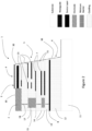
Figure 1 is a top view of a photonic chip device in accordance with an embodiment of the present disclosure; -
Figure 2 is a cross-sectional side view of the photonic chip device ofFig. 1 ; -
Figure 3 is a cross-sectional side view of the photonic chip device ofFig. 1 coupled to an optical fiber; -
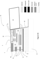
Figure 4A is a side view of a photonic chip device in accordance with another embodiment of the present disclosure; -
Figure 4B is an end view of the photonic chip device ofFig. 4A ; -
Figure 5 is a cross-sectional side view of a moisture barrier thin-film stack of the photonic chip device ofFig. 1 ; -
Figure 6 is a cross-sectional side view of an alternative moisture barrier thin-film stack of the photonic chip device ofFig. 1 ; -
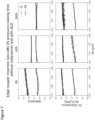
Figure 7 illustrates plots of PDL over time for unprotected photonic chip devices and protected photonic chip devices; -
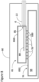
Figure 8 is a schematic cross-sectional side view of a carrier-mounted photonic chip device having the moisture barrier coating located in a non-hermetic package. - While the present teachings are described in conjunction with various embodiments and examples, it is not intended that the present teachings be limited to such embodiments. On the contrary, the present teachings encompass various alternatives and equivalents, as will be appreciated by those of skill in the art.
- With reference to
Figs. 1 to 3 , aphotonic chip 1 may include electrical input/output (IOs)pads 2, typically on anupper surface 3 of the photonic chip1, and optical input/outputs (IOs), such asoptical grating couplers 4 on theupper surface 3 and/oroptical edge couplers 5, extending into thephotonic chip 1 from anedge 6, e.g. substantially vertical side, thereof. Theoptical grating couplers 4 and theoptical edge couplers 5 extend from a surface (upper or edge) of thephotonic chip 1, and are optically coupled tooptical waveguides 7, which transmit optical signals to and/or from optical or electro-optical components, such as lasers, modulators and photodetectors on anoptical device layer 8 within thephotonic chip 1. The optical IOs are typically sensitive to moisture, because they optically interact with the outside world via an encapsulation oxide, which is moisture sensitive. - With reference to
Figs. 2 and3 , thephotonic chip 1 includes asubstrate 11, comprised of a suitable material, such as silicon; alower cladding layer 12; and anupper cladding layer 13, each of thecladding layers optical device layer 8, is formed of a suitable optical waveguide material, i.e. comprised of a material with an index of refraction higher than the surrounding lower andupper cladding layers optical device layer 8 is sandwiched between thelower cladding layer 12 and theupper cladding layer 13. Thelower cladding layer 12 may be 2.0 µm to 3.0 µm thick, while theupper cladding layer 13 may be 0.75 µm to 1.5 µm thick. - Above the
upper cladding layer 13 is a plurality of layers alternating betweenetch stop layers 14 anddielectric spacer layers 15. Theetch stop layers 14 may be formed of a suitable material, e.g. silicon nitride (Si3N4), to provide guidelines for etching eachdielectric spacer layer 15 to a predetermined depth. For example, thephotonic chip 1 may include a stack ofconductive metal structures 17, andvias 18, e.g. comprised of Al or Cu, for electrically connecting theelectrical IO pads 2 with electrical or electro-optical components in or above thedevice layer 8. Theetch stop layers 14 may be comprised of a suitable optical waveguide material, i.e. comprise a material with an index of refraction higher than thedielectric layers 15, and providing a sufficient index contrast to confine light. Accordingly, portions of theetch stop layers 14 may be configured into theoptical edge coupler 5 and theoptical waveguides 7 by etching away selected portions of the etch stop layer material leaving theoptical waveguides 7. Theoptical edge coupler 5 may be comprised of a plurality of paralleloptical waveguide segments 21 adjacent one another in the sameetch stop layer 14 and/or superposed with one another in superposed spaced-apartetch stop layers 14. Thewaveguide segments 21 may be arranged in an array, e.g. 2x2, and spaced apart into a configuration with outer ends thereof proximate theedge 6 for coupling to an external optical waveguide, e.g.,optical fiber 22. The ends of some of thewaveguide segments 21, e.g. in the upper mostetch stop layers 14 may taper down to a point, while the ends ofother waveguide segments 21 may expand to enhance evanescent coupling therebetween for transmitting optical signals through sequential superposed spaced-apartwaveguides 7 between theoptical edge coupler 5 and the optical components in theoptical device layer 8. - Similarly, the
optical grating couplers 4 may couple light upwardly from and/or downwardly towards theoptical device layer 8 utilizing a plurality ofwaveguide segments 21 superposed with one another in superposedetch stop layers 14 spaced apart bydielectric layers 15. The ends of some of thewaveguide segments 21, e.g. in the upper most etch stop layers 14 may taper down to a point, while the ends ofother waveguide segments 21 may expand to enhance evanescent coupling therebetween. Thewaveguide segments 21 optically coupling the opticalgrating couplers 4 to theoptical device layer 8 may extend perpendicular to thewaveguide segments 21 optically coupling theoptical edge coupler 5 to theoptical device layer 8. - The coupling of light between
waveguide segments 21 andwaveguides 7 may proceed downward in the layers until the light reaches thedevice layer 8. Accordingly, since theoptical device layer 8 is between theoptical edge coupler 5 and thesubstrate 11, the light remains separated from thesubstrate 11, thereby eliminating any light be lost by coupling into thesubstrate 11. - To seal the
photonic chip 1 from humidity a multi-layer thin-film stack 30 may be deposited over theentire photonic chip 1. The thin-film stack 30 may comprise at least 2 layers, preferably 3-20 layers, more preferably 8-12 layers, alternating between adielectric layer 31, also referred to herein as themoisture barrier layer 31 or a second dielectric layer, and adielectric layer 32, also referred to herein as the first dielectric layer and comprising, e.g., a first dielectric material such as silicon dioxide (SiO2). The moisture barrier layers 31 comprise a second different dielectric material with a density that is different, e.g., greater than the first dielectric material in thedielectric layers 32, and/or a material with a higher refractive index (RI) than the dielectric layers 32. Example materials for themoisture barrier layer 31 include metallic oxides, such as e.g. aluminum oxide (Al2O3) or hafnium oxide (HfO2), and semiconductor nitrides, such as silicon nitride Si3N4 and gallium nitride GaN. Each of the moisture barrier layers 31 and thedielectric layers 32 may comprise a thickness of between 4 nm and 25 nm, preferably between 5 nm and 10 nm. Normally, Al2O3 has a bulk refractive index (RI) of ~1.7, which may not be compatible with some devices, such as some embodiments of theoptical edge coupler 5, which may have effective RI of -1.5-1.6. However, athin film stack 30 including moisture barrier layers 31 comprised of Al2O3 has an effective RI that is much smaller, e.g. <1.5, which makes them compatible with theoptical edge coupler 5. Preferably, the thin-film stack 30 may be deposited using atomic layer deposition (ALD); however, other suitable methods are possible, such as sputtering, resulting in lower material quality and conformity. The oxide deposited in the back-end-of-line process (PECVD oxides) are not of very good quality partly because they are deposited at low temperature and tend to not be stoichiometric. The normal back-end-of-line oxides are also under stress from the wafer and can relax by absorbing water. In contrast ALD deposit very high quality oxide that is stoichiometric and will not typically absorb water. Accordingly, the moisture barrier layers 31, e.g. Al2O3, are better because they are denser. - Multiple interfaces of the ALD deposited moisture barrier layers 31 and the
dielectric layers 32 also helps breaking moisture paths, since the paths for water diffusion are broken each time there is new interface and material density changes. The total thickness of thestack 30 may be thinner than 100 nm, and in some embodiments thinner than 50 nm. - In bulk, the RI of Si3N4 is 2.0 and Al2O3 is 1.7, but when deposited in thin film moisture barrier layers 31 the effective refractive index changes, and tends toward the highest index in the surrounding layers, e.g. the
dielectric layers 32 of SiO2 atRI=1.5, as the thickness of the thin film moisture barrier layers 31 approaches zero. - The thin-
film stack 30 may be compatible with theoptical edge coupler 5 when the effective refractive index of the thin-film stack 30 is less than the effective refractive index of theoptical edge coupler 5, e.g. when the total thickness of the thin-film stack 30 is less than ~50 nm. If the thin-film stack 30 increases in thickness, i.e. approximately 100 nm or more, then the effective index of the thin-film stack 30 becomes comparable to the effective index of theoptical edge coupler 5, and the mode of theoptical edge coupler 5 may be affected, e.g. the mode spreads and overlaps both the original mode of theoptical edge coupler 5 and the thin-film stack 30. If the thickness of the thin-film stack 30 were to increase even further, e.g. greater than 100 nm, then the effective index of the thin-film stack 30 may be greater than the effective index of theoptical edge coupler 5 and light would be guided in the thin-film stack 30 instead of in theoptical edge coupler 5, which would be undesirable. - Preferably, the
optical edge coupler 5 is unperturbed by the thin-film stack 30; however, with reference toFigs. 4A and4B , aphotonic chip 41 may include anoptical edge coupler 45 that includes a portion of the thin-film stack 30. Thephotonic chip 41 includes most of the same elements as thephotonic chip 1, i.e. thesubstrate 11, formed of a suitable material, such as silicon; thelower cladding layer 12; and theupper cladding layer 13, each of the cladding layers 12 and 13 formed of a dielectric, e.g. oxide material, such as silicon dioxide. Theoptical device layer 8, is formed of a suitable waveguide material, i.e., a material with an index of refraction higher than the surrounding lower and upper cladding layers 12 and 13, such as a semiconductor waveguide material, e.g., silicon, silicon nitride, poly-silicon, silicon oxynitride, silicon-germanium, and/or germanium. Theoptical device layer 8 is sandwiched between thelower cladding layer 12 and theupper cladding layer 13. Thelower cladding layer 12 may be, e.g., 2.0 µm to 3.0 µm thick, while theupper cladding layer 13 may be, e.g., 0.75 µm to 1.5 µm thick. - The
optical edge coupler 45 may comprise a relatively thicker stack, e.g. 4 to 20 alternating layers with a total thickness of approximately 100 nm, similar to eachwaveguide layer 21, whereby the upper portion of the thin-film stack 30, i.e. on theupper surface 3 of thephotonic chip 41, is thick enough to perturb the field of the super-mode of light being coupled from theoptical fiber 22. Accordingly, the thin-film stack 30 may comprise an additional waveguide layer that becomes part of theoptical edge coupler 45. - When the thickness of a thin-
film stack 30 is too thick, i.e. much thicker than waveguide layers 21, the fundamental mode normally supported by theoptical edge coupler 45 is no longer the super-mode created by the waveguide arrangement, but instead becomes a mode guided in slab-like waveguide of the thin-film stack 30, which is undesirable. -
Figures 5 and6 illustrate example ALD recipes for the moisture barrier layers 31 and the dielectric layers 32. The first example of the thin-film stack 30, illustrated inFigure 5 , is about 100 nm thick total and is comprised of 10 alternating layers of, e.g., metallic oxide layers 31 (Al2O3) and dielectric layers 32 (SiO2) each approximately 10 nm thick. The second example of the thin-film stack 30, illustrated inFigure 6 , is thinner and more optically transparent, and has a total thickness of about 45 nm and is formed of 9 alternating moisture barrier layers 31 (Al2O3) and dielectric layers 32 (SiO2), each layer being approximately 5 nm thick. One of the moisture barrier layers 31 may form the innermost layer proximate theoptical edge coupler 5, and one of thedielectric layers 32 may form the outermost layer or vice versa. Alternatively, one of the moisture barrier layers 31 or one of thedielectric layers 32 may form both the innermost and outermost layers of thestack 30. In some embodiments, both the innermost and the outermost layers of thestack 30 may be layers of a same material as at least one of thelower cladding layer 12 and theupper cladding layer 13. In some embodiments, both the innermost and the outermost layers of thestack 30 may be silicon dioxide layers. - ALD is conformal and, in some embodiments, covers the
entire photonic chip 1 with themulti-layer stack 30, even regions that could have cavities, such as the ones seen when doing a silicon isotropic etch. ALD produces high quality moisture barrier layers 31 anddielectric layers 32 that have good mechanical and optical properties. Multi-layer designs break moisture diffusion paths at every interface and helps seal thephotonic chip 1. Thin layers (<50 nm and typically <25 nm) have low effective refractive indices compared to bulk thickness layers, and can be optically compatible with refractive index (RI) sensitive devices, such as opticalgrating couplers 4 andoptical edge couplers 5, even if the bulk layer's RI wouldn't be compatible. ALD may deposit themulti-layer stack 30 at low temperatures (<400 °C), which are compatible with full flow photonic chips. - With reference to
Figures 2 and3 , a method of manufacturing the PIC orphotonic chip 1 with a moisture barrier includes: providing or forming thephotonic chip 1 on thesubstrate 11. Thephotonic chip 1 includes theoptical device layer 8 sandwiched between thelower cladding layer 12 and theupper cladding layer 13. The optical input/output (IO), e.g. in the form of an opticalgrating coupler 4 and/or anoptical edge coupler 5, is provided or formed above theoptical device layer 8 enabling light to be transmitted to and/or from the optical device layer from the near end of an external waveguide, e.g. theoptical fiber 22. Theelectrical IO pads 2 are provided on theupper surface 3 with a plurality of superposedmetallic contact structures 17 and vias 18 electrically connecting thepads 2 with components on theoptical device layer 8. - Forming the electrical connector structure may comprise: a) depositing an
etch stop layer 14; b) depositing adielectric layer 15 over theetch stop layer 14; c) etching an opening in thedielectric layer 15 down to theetch stop layer 14; d) depositing metal in the opening to form one or more of themetallic contact structures 17; and repeating steps a) to d) to form the plurality of superposedmetallic contact structures 17 stacked above theoptical device layer 8. - Preferably but not exclusively, the
optical edge coupler 5 andwaveguide segments optical device layer 8 may be formed from etch stop layers 14 provided in thephotonic chip 1 for defining themetallic contact structures 17. - The thin-
film stack 30 may be applied over theentire photonic chip 1, e.g. with ALD encapsulation (Fig. 2 ). The thin-film stack 30 is conformal and may cover features on thetop surface 3 of thephotonic chip 1, e.g. theelectrical IO pads 2, but also would cover etch facets (~10°) on theedge 6 of thephotonic chip 1, and bottom-of-chip features, such as the interface for thesubstrate 11 and thePIC 1, e.g.lower cladding layer 12. Subsequent etching steps (Fig. 3 ) are performed to remove portions of the thin-film stack 30 from theelectrical IO pads 2 to enable probing/wire-bonding/bumping thereto. The thin-film stack 30 may be thin enough such that it does not affect the optical IOs, e.g. opticalgrating coupler 4 oroptical edge coupler 5; however, the thin-film stack should also be thick enough to shield thephotonic chip 1 from moisture. - The top row of plots, provided in
Fig. 7 , illustrate the insertion loss of anoptical edge coupler 5 in (dB) as a function of time in a pressure cooker, i.e. a high temperature & humidity environment without a moisture barrier. Both the wavelength dependency and the PDL changes over time, which is undesirable. The second row of plots shows aphotonic chip 1 encapsulated with a moisture barrier formed by the thin-film stack 30, and illustrates a much more stable operation of the device over time. -
Fig. 8 illustrates aphotonic chip 81 fixedly attached along a facingsurface 91 of acarrier substrate 90. Thephotonic chip 81 may be an embodiment of thephotonic chip 1 or thephotonic chip 41 described above. Thephotonic chip 81 includes at least anoptical waveguide 88 terminating at anedge 6 of the chip to form anoptical edge coupler 85. Theoptical edge coupler 85 may be an embodiment of theoptical edge coupler 5 or theoptical edge coupler 45 described above, and is configured for optically coupling to a near end of anoptical fiber 22. An ALD-applied coating stack 830 ("coating 830") covers at least theedge 6 of the chip and at least a portion of the facingsurface 91 to form a moisture-protective barrier. Thecoating 830 may be e.g. as described above with reference to the moisture barriermulti-layer stack 30. Thecoating 830 may include a stack of interleaving first and second dielectric layers of different material composition, e.g. layers 31 and 32 as described above, the stack including at least 2 pairs of the layers, with at least three 3 interfaces between adjacent ones of the first and second layers therein. In the illustrated embodiment, thephotonic chip 81 is attached to thesurface 91 of thecarrier 90 with one or more metal, e.g. copper,pillars 95, e.g., via solder. Furthermore, in the illustrated embodiment, thecoating 30 is applied to the chip-carrier assembly 81/90 using the ALD at a low enough temperature to preserve any previous soldering. The ALD-appliedcoating 830 conforms to all exposed surfaces of the assembly, as shown in the illustrated example, desirably provided an effective barrier to external moisture. The chip-carrier assembly 81/90 may therefore be disposed within anon-hermetic housing 80. - The foregoing description of one or more embodiments of the invention has been presented for the purposes of illustration and description. It is not intended to be exhaustive or to limit the invention to the precise form disclosed. Many modifications and variations are possible in light of the above teaching. For example, various features described above with reference to the
photonic chip 1, e.g. the optical grating coupler(s) 4, theelectrical IO pads 2, thedevice layer 8, may be absent in other embodiments. Furthermore, in some embodiments theoptical edge coupler 5 may be formed without thesegments 21, e.g. by an end of theoptical waveguide 7 or of thedevice layer 8 that is proximate to thechip edge 6, e.g. terminating at theedge 6. In some embodiments theoptical edge coupler 5 may be configured for coupling to a waveguide of another optical device, e.g. to an end of an optical waveguide of another optical chip, with or without one or more coupling optical elements therebetween. In some embodiments, thecoating 30 may cover only a portion, e.g. half or more, of the surface of the photonic chip. In some embodiments, thecoating 30 may be up to 150 nm thick. - Furthermore, although the
first layers 31 are referred to herein as moisture barrier layers, the underlying physical mechanism preventing moisture to penetrate thecoating 30 may be related mostly, or to at least in part, to theinterfaces 31/32 between the first (32) and second (31) layers of different material composition, rather than to thelayers 31 themselves and thicknesses thereof. Accordingly, relativelythin layers 31, e.g. 4-10 nanometers thick layers of, e.g, SiN, may provide an effective moisture barrier in embodiments with a suitable number of the layer interfaces 31/32, e.g. at least 3, or preferably 4-10 or moresuch interfaces 31/32 The first layers 32, typically having a smaller refractive index, e.g. SiO2 layers, may be thicker than thesecond layers 31, e.g. 10-20 nm. - According to example embodiments disclosed above, e.g., in the summary section and/or in reference to any one or any combination of some or all of
FIGs. 1-7 , provided is an apparatus comprising a photonic chip (e.g. 1,Figs. 1-3 , 41,Figs. 4A ,4B , 81,Fig. 8 ), the photonic chip comprising an edge optical coupler (e.g. 5,Figs. 1-3 , 45,Figs. 4A ,4B , 85Fig. 8 ) for end-coupling an external optical waveguide to the photonic chip, the optical coupler having one end at an edge (e.g. 6,Figs. 1-3 ,8 ), of the chip; and a coating (e.g. 30,Figs. 1-6 , 830Fig. 8 ) on, at least, a part of the edge of the chip over the one end of the optical edge coupler, the coating being a stack alternating first and second dielectric layers (e.g. 31 and 32,Figs. 5 ,6 ) of different material composition, the stack including at least 2 interfaces between adjacent ones of the first and second layers. - The external optical waveguide may be an optical fiber or an optical waveguide of an external optical device, e.g. another photonic chip. Herein, the optical edge coupler(s) can optically couple to the external optical waveguide via an end thereof located near to an outside edge of the photonic chip and/or located near to an internal edge of the photonic chip. In some implementations, the edge of the photonic chip may be an edge of a recess in the photonic chip in which an external device, such as a laser, is inserted, so that an end of an optical waveguide of the external device is nearby, and optically coupled to, an optical edge coupler at the edge of the recess.
- In some embodiments of the above apparatus, the coating (e.g. 30,
Figs. 1-6 ) has a thickness of 10 to 150 nanometers. In some embodiments of the above apparatus, the coating covers at least half of a surface of the photonic chip. In some embodiments of the above apparatus, each second layer (e.g. 31,Figs. 5 ,6 ) of the coating is thinner than each first layer (e.g. 32,Figs. 5 ,6 ). In some embodiments of the above apparatus, each second layer is one of a silicon nitride layer, a hafnium oxide layer, and an aluminum oxide layer. In some embodiments of the above apparatus, each first layer is a silicon-oxide layer. In some embodiments, the stack starts and ends with a silicon dioxide layer. - Some embodiments of the above apparatus comprise a carrier, and the photonic chip is attached along a facing major planar surface of the carrier, with the coating being disposed over at least a part of the surface. In some embodiments of the above apparatus, the stack has at least four of the layers. In some embodiments of the above apparatus, each second layer is thinner than each first layer of the stack. In some embodiments of the above apparatus, the coating has a thickness of less than 100 nanometers.
- Some embodiments of the above apparatus may further comprise a non-hermetic package including the substrate, the photonic chip being mounted on a surface the substrate and being located in the package, the coating substantial protecting the optical edge coupler from ambient moisture.
- According to another example embodiment disclosed above, e.g., in the summary section and/or in reference to any one or any combination of some or all of
FIGs. 1-7 , provided is a method comprising performing atomic layer deposition (ALD) to coat at least part of an edge of a photonic chip with a stack of at least three dielectric layers, adjacent ones of the dielectric layers of the stack having different material compositions. In some embodiments of the above method, the part is adjacent one end of an optical fiber coupler located in the photonic chip. In some embodiments of the above method, the performing produces the stack such that thicknesses of the layers of the stack alternate thereacross. In some embodiments of the above method, the atomic layer deposition is performed after soldering the photonic chip to a carrier. - Unless explicitly stated otherwise, each numerical value and range in the above description should be interpreted as being approximate as if the word "about" or "approximately" preceded the value or range.
- Various modifications of the described embodiments, as well as other embodiments within the scope of the disclosure, which are apparent to persons skilled in the art to which the disclosure pertains are deemed to lie within the principle and scope of the disclosure, e.g., as expressed in the following claims. It is thus intended that the scope of the invention be limited not by this detailed description, but rather by the claims appended hereto.
Claims (16)
- An apparatus comprising:a photonic chip comprising an optical edge coupler for end-coupling an external optical waveguide to the photonic chip, the optical coupler having one end at an edge of the chip; anda coating on, at least, a part of the edge of the chip over the one end of the optical edge coupler, the coating being a stack interleaving first and second dielectric layers of different material composition, the stack including at least 2 interfaces between adjacent ones of the first and second layers.
- The apparatus of claim 1, wherein the coating covers at least half of a surface of the photonic chip.
- The apparatus of claim 1, wherein the external optical waveguide is an optical fiber.
- The apparatus of claim 1, wherein each second layer is one of a silicon nitride layer, aluminum oxide layer, and a hafnium oxide layer.
- The apparatus of claim 4, wherein each first layer is a silicon-oxide layer.
- The apparatus of claim 5, wherein each second layer is thinner than each first layer.
- The apparatus of claim 1, wherein the stack starts and ends with a silicon-dioxide layer.
- The apparatus of claim 1 comprising a carrier, wherein the photonic chip is attached along a facing surface of the carrier; and wherein the coating is disposed over at least a part of the surface.
- The apparatus of clam 1, wherein the stack has at least four of the layers.
- The apparatus of claim 1, wherein each of the layers is less than 25 nm thick.
- The apparatus of claim 1, wherein the coating has a thickness of less than 100 nanometers.
- The apparatus of claim 1, further comprising a non-hermetic package including a substrate, the photonic chip being mounted on a surface of the substrate and being located in the package, the coating substantially protecting the optical edge coupler from ambient moisture.
- A method comprising:
performing atomic layer deposition to coat at least a part of an edge of a photonic chip with a stack of at least three dielectric layers, adjacent ones of the dielectric layers having different material compositions. - The method of claim 13, wherein the part is adjacent one end of an optical fiber coupler located in the photonic chip.
- The method of claim 13, wherein the performing produces the stack such that thicknesses of the layers of the stack alternate thereacross.
- The method of claim 13, wherein the atomic layer deposition is performed after soldering the photonic chip to a carrier.
Applications Claiming Priority (1)
| Application Number | Priority Date | Filing Date | Title |
|---|---|---|---|
| FI20235261A FI20235261A1 (en) | 2023-03-06 | 2023-03-06 | Optical coupler moisture barrier |
Publications (1)
| Publication Number | Publication Date |
|---|---|
| EP4428590A1 true EP4428590A1 (en) | 2024-09-11 |
Family
ID=90124019
Family Applications (1)
| Application Number | Title | Priority Date | Filing Date |
|---|---|---|---|
| EP24160753.0A Pending EP4428590A1 (en) | 2023-03-06 | 2024-03-01 | Optical coupler moisture barrier |
Country Status (3)
| Country | Link |
|---|---|
| US (1) | US20240302595A1 (en) |
| EP (1) | EP4428590A1 (en) |
| FI (1) | FI20235261A1 (en) |
Citations (6)
| Publication number | Priority date | Publication date | Assignee | Title |
|---|---|---|---|---|
| US20140092931A1 (en) * | 2012-04-04 | 2014-04-03 | Osram Opto Semiconductors Gmbh | Laser Diode Assembly |
| US20150097257A1 (en) * | 2013-10-04 | 2015-04-09 | International Business Machines Corporation | Integrated waveguide structure with perforated chip edge seal |
| US20160147020A1 (en) * | 2013-07-24 | 2016-05-26 | Effect Photonics B.V. | Optical subassembly, optical system and method |
| US20220187638A1 (en) * | 2020-12-14 | 2022-06-16 | Lightwave Logic Inc | Hybrid eo polymer modulator with ald sealant layer |
| US20220269003A1 (en) * | 2020-07-09 | 2022-08-25 | Taiwan Semiconductor Manufacturing Co., Ltd. | Photonic device |
| US20230069212A1 (en) * | 2021-08-30 | 2023-03-02 | Taiwan Semiconductor Manufacturing Company Limited | Optical integrated circuit structure including edge coupling protective features and methods of forming same |
Family Cites Families (2)
| Publication number | Priority date | Publication date | Assignee | Title |
|---|---|---|---|---|
| US7303339B2 (en) * | 2002-08-28 | 2007-12-04 | Phosistor Technologies, Inc. | Optical beam transformer module for light coupling between a fiber array and a photonic chip and the method of making the same |
| US12405423B2 (en) * | 2022-10-03 | 2025-09-02 | Globalfoundries U.S. Inc. | Hybrid edge couplers with voids |
-
2023
- 2023-03-06 FI FI20235261A patent/FI20235261A1/en unknown
-
2024
- 2024-03-01 EP EP24160753.0A patent/EP4428590A1/en active Pending
- 2024-03-04 US US18/594,415 patent/US20240302595A1/en active Pending
Patent Citations (7)
| Publication number | Priority date | Publication date | Assignee | Title |
|---|---|---|---|---|
| US20140092931A1 (en) * | 2012-04-04 | 2014-04-03 | Osram Opto Semiconductors Gmbh | Laser Diode Assembly |
| US20160147020A1 (en) * | 2013-07-24 | 2016-05-26 | Effect Photonics B.V. | Optical subassembly, optical system and method |
| US9766406B2 (en) * | 2013-07-24 | 2017-09-19 | Effect Photonics B.V. | Optical subassembly, optical system and method |
| US20150097257A1 (en) * | 2013-10-04 | 2015-04-09 | International Business Machines Corporation | Integrated waveguide structure with perforated chip edge seal |
| US20220269003A1 (en) * | 2020-07-09 | 2022-08-25 | Taiwan Semiconductor Manufacturing Co., Ltd. | Photonic device |
| US20220187638A1 (en) * | 2020-12-14 | 2022-06-16 | Lightwave Logic Inc | Hybrid eo polymer modulator with ald sealant layer |
| US20230069212A1 (en) * | 2021-08-30 | 2023-03-02 | Taiwan Semiconductor Manufacturing Company Limited | Optical integrated circuit structure including edge coupling protective features and methods of forming same |
Also Published As
| Publication number | Publication date |
|---|---|
| FI20235261A1 (en) | 2024-09-07 |
| US20240302595A1 (en) | 2024-09-12 |
Similar Documents
| Publication | Publication Date | Title |
|---|---|---|
| CN100403082C (en) | Optoelectronic package and method of fabrication | |
| KR101296833B1 (en) | Silicon Photonics Chip | |
| US20020181838A1 (en) | Optical MEMS device and package having a light-transmissive opening or window | |
| US9042691B2 (en) | Optical coupling module for silicon photonics chip | |
| US10193302B2 (en) | Light engine with integrated turning mirror for direct coupling to photonically-enabled complementary metal-oxide semiconductor (CMOS) die | |
| EP4202511B1 (en) | Optical edge coupler having a heterogeneous cladding structure | |
| KR102843552B1 (en) | Mechanisms that transfer light between layers of multi-chip photonic assemblies | |
| JP2012014039A (en) | Wavelength multiplexer/demultiplexer and method of manufacturing the same | |
| US11280971B2 (en) | Optical coupling with undercut protection from underfill | |
| JP2003014964A (en) | Optical element and optical transceiver and other optical devices using the optical element | |
| CN1885079B (en) | Optical device | |
| US7003192B2 (en) | Micro opto electro mechanical device | |
| US20240302595A1 (en) | Optical coupler moisture barrier | |
| JPWO2003083542A1 (en) | Optical device and manufacturing method thereof | |
| US7195402B2 (en) | Optical device | |
| WO2025050726A1 (en) | Photonic integrated circuit chip and silicon photonics integrated platform | |
| JP2004296761A (en) | Semiconductor device | |
| JPH03191572A (en) | Optical semiconductor device | |
| CN211555854U (en) | Packaging structure and semiconductor device | |
| US11506918B2 (en) | Hybrid EO polymer modulator with ALD sealant layer | |
| US12092874B2 (en) | Silicon photonic package and method of fabricating the same | |
| US20260118602A1 (en) | Semiconductor package including optical structure and waveguide | |
| TWI892285B (en) | Optical signal measurement apparatus and method of manufacturing the same, and optical signal measurement method | |
| TWI889060B (en) | Packaging structure and manufacturing method thereof | |
| US20260056376A1 (en) | Chip structure and semiconductor package including the same |
Legal Events
| Date | Code | Title | Description |
|---|---|---|---|
| PUAI | Public reference made under article 153(3) epc to a published international application that has entered the european phase |
Free format text: ORIGINAL CODE: 0009012 |
|
| STAA | Information on the status of an ep patent application or granted ep patent |
Free format text: STATUS: THE APPLICATION HAS BEEN PUBLISHED |
|
| AK | Designated contracting states |
Kind code of ref document: A1 Designated state(s): AL AT BE BG CH CY CZ DE DK EE ES FI FR GB GR HR HU IE IS IT LI LT LU LV MC ME MK MT NL NO PL PT RO RS SE SI SK SM TR |
|
| STAA | Information on the status of an ep patent application or granted ep patent |
Free format text: STATUS: REQUEST FOR EXAMINATION WAS MADE |
|
| 17P | Request for examination filed |
Effective date: 20250311 |