EP4426075A1 - Ceramic copper circuit board and semiconductor device using same - Google Patents
Ceramic copper circuit board and semiconductor device using same Download PDFInfo
- Publication number
- EP4426075A1 EP4426075A1 EP22886798.2A EP22886798A EP4426075A1 EP 4426075 A1 EP4426075 A1 EP 4426075A1 EP 22886798 A EP22886798 A EP 22886798A EP 4426075 A1 EP4426075 A1 EP 4426075A1
- Authority
- EP
- European Patent Office
- Prior art keywords
- copper circuit
- jutting
- mass
- ceramic
- less
- Prior art date
- Legal status (The legal status is an assumption and is not a legal conclusion. Google has not performed a legal analysis and makes no representation as to the accuracy of the status listed.)
- Pending
Links
Images

Classifications
-
- H—ELECTRICITY
- H05—ELECTRIC TECHNIQUES NOT OTHERWISE PROVIDED FOR
- H05K—PRINTED CIRCUITS; CASINGS OR CONSTRUCTIONAL DETAILS OF ELECTRIC APPARATUS; MANUFACTURE OF ASSEMBLAGES OF ELECTRICAL COMPONENTS
- H05K1/00—Printed circuits
- H05K1/02—Details
- H05K1/03—Use of materials for the substrate
-
- C—CHEMISTRY; METALLURGY
- C04—CEMENTS; CONCRETE; ARTIFICIAL STONE; CERAMICS; REFRACTORIES
- C04B—LIME, MAGNESIA; SLAG; CEMENTS; COMPOSITIONS THEREOF, e.g. MORTARS, CONCRETE OR LIKE BUILDING MATERIALS; ARTIFICIAL STONE; CERAMICS; REFRACTORIES; TREATMENT OF NATURAL STONE
- C04B37/00—Joining burned ceramic articles with other burned ceramic articles or other articles by heating
- C04B37/02—Joining burned ceramic articles with other burned ceramic articles or other articles by heating with metallic articles
- C04B37/023—Joining burned ceramic articles with other burned ceramic articles or other articles by heating with metallic articles characterised by the interlayer used
- C04B37/026—Joining burned ceramic articles with other burned ceramic articles or other articles by heating with metallic articles characterised by the interlayer used consisting of metals or metal salts
-
- H—ELECTRICITY
- H05—ELECTRIC TECHNIQUES NOT OTHERWISE PROVIDED FOR
- H05K—PRINTED CIRCUITS; CASINGS OR CONSTRUCTIONAL DETAILS OF ELECTRIC APPARATUS; MANUFACTURE OF ASSEMBLAGES OF ELECTRICAL COMPONENTS
- H05K1/00—Printed circuits
- H05K1/02—Details
- H05K1/0201—Thermal arrangements, e.g. for cooling, heating or preventing overheating
- H05K1/0203—Cooling of mounted components
-
- H—ELECTRICITY
- H05—ELECTRIC TECHNIQUES NOT OTHERWISE PROVIDED FOR
- H05K—PRINTED CIRCUITS; CASINGS OR CONSTRUCTIONAL DETAILS OF ELECTRIC APPARATUS; MANUFACTURE OF ASSEMBLAGES OF ELECTRICAL COMPONENTS
- H05K1/00—Printed circuits
- H05K1/02—Details
- H05K1/03—Use of materials for the substrate
- H05K1/0306—Inorganic insulating substrates, e.g. ceramic, glass
-
- H—ELECTRICITY
- H05—ELECTRIC TECHNIQUES NOT OTHERWISE PROVIDED FOR
- H05K—PRINTED CIRCUITS; CASINGS OR CONSTRUCTIONAL DETAILS OF ELECTRIC APPARATUS; MANUFACTURE OF ASSEMBLAGES OF ELECTRICAL COMPONENTS
- H05K1/00—Printed circuits
- H05K1/02—Details
- H05K1/09—Use of materials for the conductive, e.g. metallic pattern
-
- H—ELECTRICITY
- H05—ELECTRIC TECHNIQUES NOT OTHERWISE PROVIDED FOR
- H05K—PRINTED CIRCUITS; CASINGS OR CONSTRUCTIONAL DETAILS OF ELECTRIC APPARATUS; MANUFACTURE OF ASSEMBLAGES OF ELECTRICAL COMPONENTS
- H05K3/00—Apparatus or processes for manufacturing printed circuits
- H05K3/02—Apparatus or processes for manufacturing printed circuits in which the conductive material is applied to the surface of the insulating support and is thereafter removed from such areas of the surface which are not intended for current conducting or shielding
- H05K3/022—Processes for manufacturing precursors of printed circuits, i.e. copper-clad substrates
-
- H—ELECTRICITY
- H10—SEMICONDUCTOR DEVICES; ELECTRIC SOLID-STATE DEVICES NOT OTHERWISE PROVIDED FOR
- H10W—GENERIC PACKAGES, INTERCONNECTIONS, CONNECTORS OR OTHER CONSTRUCTIONAL DETAILS OF DEVICES COVERED BY CLASS H10
- H10W70/00—Package substrates; Interposers; Redistribution layers [RDL]
- H10W70/60—Insulating or insulated package substrates; Interposers; Redistribution layers
- H10W70/67—Insulating or insulated package substrates; Interposers; Redistribution layers characterised by their insulating layers or insulating parts
- H10W70/68—Shapes or dispositions thereof
-
- C—CHEMISTRY; METALLURGY
- C04—CEMENTS; CONCRETE; ARTIFICIAL STONE; CERAMICS; REFRACTORIES
- C04B—LIME, MAGNESIA; SLAG; CEMENTS; COMPOSITIONS THEREOF, e.g. MORTARS, CONCRETE OR LIKE BUILDING MATERIALS; ARTIFICIAL STONE; CERAMICS; REFRACTORIES; TREATMENT OF NATURAL STONE
- C04B2235/00—Aspects relating to ceramic starting mixtures or sintered ceramic products
- C04B2235/02—Composition of constituents of the starting material or of secondary phases of the final product
- C04B2235/50—Constituents or additives of the starting mixture chosen for their shape or used because of their shape or their physical appearance
- C04B2235/54—Particle size related information
- C04B2235/5418—Particle size related information expressed by the size of the particles or aggregates thereof
- C04B2235/5436—Particle size related information expressed by the size of the particles or aggregates thereof micrometer sized, i.e. from 1 to 100 micron
-
- C—CHEMISTRY; METALLURGY
- C04—CEMENTS; CONCRETE; ARTIFICIAL STONE; CERAMICS; REFRACTORIES
- C04B—LIME, MAGNESIA; SLAG; CEMENTS; COMPOSITIONS THEREOF, e.g. MORTARS, CONCRETE OR LIKE BUILDING MATERIALS; ARTIFICIAL STONE; CERAMICS; REFRACTORIES; TREATMENT OF NATURAL STONE
- C04B2235/00—Aspects relating to ceramic starting mixtures or sintered ceramic products
- C04B2235/65—Aspects relating to heat treatments of ceramic bodies such as green ceramics or pre-sintered ceramics, e.g. burning, sintering or melting processes
- C04B2235/656—Aspects relating to heat treatments of ceramic bodies such as green ceramics or pre-sintered ceramics, e.g. burning, sintering or melting processes characterised by specific heating conditions during heat treatment
- C04B2235/6562—Heating rate
-
- C—CHEMISTRY; METALLURGY
- C04—CEMENTS; CONCRETE; ARTIFICIAL STONE; CERAMICS; REFRACTORIES
- C04B—LIME, MAGNESIA; SLAG; CEMENTS; COMPOSITIONS THEREOF, e.g. MORTARS, CONCRETE OR LIKE BUILDING MATERIALS; ARTIFICIAL STONE; CERAMICS; REFRACTORIES; TREATMENT OF NATURAL STONE
- C04B2235/00—Aspects relating to ceramic starting mixtures or sintered ceramic products
- C04B2235/65—Aspects relating to heat treatments of ceramic bodies such as green ceramics or pre-sintered ceramics, e.g. burning, sintering or melting processes
- C04B2235/656—Aspects relating to heat treatments of ceramic bodies such as green ceramics or pre-sintered ceramics, e.g. burning, sintering or melting processes characterised by specific heating conditions during heat treatment
- C04B2235/6565—Cooling rate
-
- C—CHEMISTRY; METALLURGY
- C04—CEMENTS; CONCRETE; ARTIFICIAL STONE; CERAMICS; REFRACTORIES
- C04B—LIME, MAGNESIA; SLAG; CEMENTS; COMPOSITIONS THEREOF, e.g. MORTARS, CONCRETE OR LIKE BUILDING MATERIALS; ARTIFICIAL STONE; CERAMICS; REFRACTORIES; TREATMENT OF NATURAL STONE
- C04B2235/00—Aspects relating to ceramic starting mixtures or sintered ceramic products
- C04B2235/70—Aspects relating to sintered or melt-casted ceramic products
- C04B2235/72—Products characterised by the absence or the low content of specific components, e.g. alkali metal free alumina ceramics
- C04B2235/721—Carbon content
-
- C—CHEMISTRY; METALLURGY
- C04—CEMENTS; CONCRETE; ARTIFICIAL STONE; CERAMICS; REFRACTORIES
- C04B—LIME, MAGNESIA; SLAG; CEMENTS; COMPOSITIONS THEREOF, e.g. MORTARS, CONCRETE OR LIKE BUILDING MATERIALS; ARTIFICIAL STONE; CERAMICS; REFRACTORIES; TREATMENT OF NATURAL STONE
- C04B2235/00—Aspects relating to ceramic starting mixtures or sintered ceramic products
- C04B2235/70—Aspects relating to sintered or melt-casted ceramic products
- C04B2235/72—Products characterised by the absence or the low content of specific components, e.g. alkali metal free alumina ceramics
- C04B2235/723—Oxygen content
-
- C—CHEMISTRY; METALLURGY
- C04—CEMENTS; CONCRETE; ARTIFICIAL STONE; CERAMICS; REFRACTORIES
- C04B—LIME, MAGNESIA; SLAG; CEMENTS; COMPOSITIONS THEREOF, e.g. MORTARS, CONCRETE OR LIKE BUILDING MATERIALS; ARTIFICIAL STONE; CERAMICS; REFRACTORIES; TREATMENT OF NATURAL STONE
- C04B2235/00—Aspects relating to ceramic starting mixtures or sintered ceramic products
- C04B2235/70—Aspects relating to sintered or melt-casted ceramic products
- C04B2235/96—Properties of ceramic products, e.g. mechanical properties such as strength, toughness, wear resistance
-
- C—CHEMISTRY; METALLURGY
- C04—CEMENTS; CONCRETE; ARTIFICIAL STONE; CERAMICS; REFRACTORIES
- C04B—LIME, MAGNESIA; SLAG; CEMENTS; COMPOSITIONS THEREOF, e.g. MORTARS, CONCRETE OR LIKE BUILDING MATERIALS; ARTIFICIAL STONE; CERAMICS; REFRACTORIES; TREATMENT OF NATURAL STONE
- C04B2235/00—Aspects relating to ceramic starting mixtures or sintered ceramic products
- C04B2235/70—Aspects relating to sintered or melt-casted ceramic products
- C04B2235/96—Properties of ceramic products, e.g. mechanical properties such as strength, toughness, wear resistance
- C04B2235/9607—Thermal properties, e.g. thermal expansion coefficient
-
- C—CHEMISTRY; METALLURGY
- C04—CEMENTS; CONCRETE; ARTIFICIAL STONE; CERAMICS; REFRACTORIES
- C04B—LIME, MAGNESIA; SLAG; CEMENTS; COMPOSITIONS THEREOF, e.g. MORTARS, CONCRETE OR LIKE BUILDING MATERIALS; ARTIFICIAL STONE; CERAMICS; REFRACTORIES; TREATMENT OF NATURAL STONE
- C04B2237/00—Aspects relating to ceramic laminates or to joining of ceramic articles with other articles by heating
- C04B2237/02—Aspects relating to interlayers, e.g. used to join ceramic articles with other articles by heating
- C04B2237/12—Metallic interlayers
-
- C—CHEMISTRY; METALLURGY
- C04—CEMENTS; CONCRETE; ARTIFICIAL STONE; CERAMICS; REFRACTORIES
- C04B—LIME, MAGNESIA; SLAG; CEMENTS; COMPOSITIONS THEREOF, e.g. MORTARS, CONCRETE OR LIKE BUILDING MATERIALS; ARTIFICIAL STONE; CERAMICS; REFRACTORIES; TREATMENT OF NATURAL STONE
- C04B2237/00—Aspects relating to ceramic laminates or to joining of ceramic articles with other articles by heating
- C04B2237/02—Aspects relating to interlayers, e.g. used to join ceramic articles with other articles by heating
- C04B2237/12—Metallic interlayers
- C04B2237/122—Metallic interlayers based on refractory metals
-
- C—CHEMISTRY; METALLURGY
- C04—CEMENTS; CONCRETE; ARTIFICIAL STONE; CERAMICS; REFRACTORIES
- C04B—LIME, MAGNESIA; SLAG; CEMENTS; COMPOSITIONS THEREOF, e.g. MORTARS, CONCRETE OR LIKE BUILDING MATERIALS; ARTIFICIAL STONE; CERAMICS; REFRACTORIES; TREATMENT OF NATURAL STONE
- C04B2237/00—Aspects relating to ceramic laminates or to joining of ceramic articles with other articles by heating
- C04B2237/02—Aspects relating to interlayers, e.g. used to join ceramic articles with other articles by heating
- C04B2237/12—Metallic interlayers
- C04B2237/124—Metallic interlayers based on copper
-
- C—CHEMISTRY; METALLURGY
- C04—CEMENTS; CONCRETE; ARTIFICIAL STONE; CERAMICS; REFRACTORIES
- C04B—LIME, MAGNESIA; SLAG; CEMENTS; COMPOSITIONS THEREOF, e.g. MORTARS, CONCRETE OR LIKE BUILDING MATERIALS; ARTIFICIAL STONE; CERAMICS; REFRACTORIES; TREATMENT OF NATURAL STONE
- C04B2237/00—Aspects relating to ceramic laminates or to joining of ceramic articles with other articles by heating
- C04B2237/02—Aspects relating to interlayers, e.g. used to join ceramic articles with other articles by heating
- C04B2237/12—Metallic interlayers
- C04B2237/126—Metallic interlayers wherein the active component for bonding is not the largest fraction of the interlayer
- C04B2237/127—The active component for bonding being a refractory metal
-
- C—CHEMISTRY; METALLURGY
- C04—CEMENTS; CONCRETE; ARTIFICIAL STONE; CERAMICS; REFRACTORIES
- C04B—LIME, MAGNESIA; SLAG; CEMENTS; COMPOSITIONS THEREOF, e.g. MORTARS, CONCRETE OR LIKE BUILDING MATERIALS; ARTIFICIAL STONE; CERAMICS; REFRACTORIES; TREATMENT OF NATURAL STONE
- C04B2237/00—Aspects relating to ceramic laminates or to joining of ceramic articles with other articles by heating
- C04B2237/30—Composition of layers of ceramic laminates or of ceramic or metallic articles to be joined by heating, e.g. Si substrates
- C04B2237/32—Ceramic
- C04B2237/34—Oxidic
- C04B2237/343—Alumina or aluminates
-
- C—CHEMISTRY; METALLURGY
- C04—CEMENTS; CONCRETE; ARTIFICIAL STONE; CERAMICS; REFRACTORIES
- C04B—LIME, MAGNESIA; SLAG; CEMENTS; COMPOSITIONS THEREOF, e.g. MORTARS, CONCRETE OR LIKE BUILDING MATERIALS; ARTIFICIAL STONE; CERAMICS; REFRACTORIES; TREATMENT OF NATURAL STONE
- C04B2237/00—Aspects relating to ceramic laminates or to joining of ceramic articles with other articles by heating
- C04B2237/30—Composition of layers of ceramic laminates or of ceramic or metallic articles to be joined by heating, e.g. Si substrates
- C04B2237/32—Ceramic
- C04B2237/34—Oxidic
- C04B2237/345—Refractory metal oxides
- C04B2237/348—Zirconia, hafnia, zirconates or hafnates
-
- C—CHEMISTRY; METALLURGY
- C04—CEMENTS; CONCRETE; ARTIFICIAL STONE; CERAMICS; REFRACTORIES
- C04B—LIME, MAGNESIA; SLAG; CEMENTS; COMPOSITIONS THEREOF, e.g. MORTARS, CONCRETE OR LIKE BUILDING MATERIALS; ARTIFICIAL STONE; CERAMICS; REFRACTORIES; TREATMENT OF NATURAL STONE
- C04B2237/00—Aspects relating to ceramic laminates or to joining of ceramic articles with other articles by heating
- C04B2237/30—Composition of layers of ceramic laminates or of ceramic or metallic articles to be joined by heating, e.g. Si substrates
- C04B2237/32—Ceramic
- C04B2237/36—Non-oxidic
- C04B2237/366—Aluminium nitride
-
- C—CHEMISTRY; METALLURGY
- C04—CEMENTS; CONCRETE; ARTIFICIAL STONE; CERAMICS; REFRACTORIES
- C04B—LIME, MAGNESIA; SLAG; CEMENTS; COMPOSITIONS THEREOF, e.g. MORTARS, CONCRETE OR LIKE BUILDING MATERIALS; ARTIFICIAL STONE; CERAMICS; REFRACTORIES; TREATMENT OF NATURAL STONE
- C04B2237/00—Aspects relating to ceramic laminates or to joining of ceramic articles with other articles by heating
- C04B2237/30—Composition of layers of ceramic laminates or of ceramic or metallic articles to be joined by heating, e.g. Si substrates
- C04B2237/32—Ceramic
- C04B2237/36—Non-oxidic
- C04B2237/368—Silicon nitride
-
- C—CHEMISTRY; METALLURGY
- C04—CEMENTS; CONCRETE; ARTIFICIAL STONE; CERAMICS; REFRACTORIES
- C04B—LIME, MAGNESIA; SLAG; CEMENTS; COMPOSITIONS THEREOF, e.g. MORTARS, CONCRETE OR LIKE BUILDING MATERIALS; ARTIFICIAL STONE; CERAMICS; REFRACTORIES; TREATMENT OF NATURAL STONE
- C04B2237/00—Aspects relating to ceramic laminates or to joining of ceramic articles with other articles by heating
- C04B2237/30—Composition of layers of ceramic laminates or of ceramic or metallic articles to be joined by heating, e.g. Si substrates
- C04B2237/40—Metallic
- C04B2237/407—Copper
-
- C—CHEMISTRY; METALLURGY
- C04—CEMENTS; CONCRETE; ARTIFICIAL STONE; CERAMICS; REFRACTORIES
- C04B—LIME, MAGNESIA; SLAG; CEMENTS; COMPOSITIONS THEREOF, e.g. MORTARS, CONCRETE OR LIKE BUILDING MATERIALS; ARTIFICIAL STONE; CERAMICS; REFRACTORIES; TREATMENT OF NATURAL STONE
- C04B2237/00—Aspects relating to ceramic laminates or to joining of ceramic articles with other articles by heating
- C04B2237/50—Processing aspects relating to ceramic laminates or to the joining of ceramic articles with other articles by heating
- C04B2237/70—Forming laminates or joined articles comprising layers of a specific, unusual thickness
- C04B2237/704—Forming laminates or joined articles comprising layers of a specific, unusual thickness of one or more of the ceramic layers or articles
-
- C—CHEMISTRY; METALLURGY
- C04—CEMENTS; CONCRETE; ARTIFICIAL STONE; CERAMICS; REFRACTORIES
- C04B—LIME, MAGNESIA; SLAG; CEMENTS; COMPOSITIONS THEREOF, e.g. MORTARS, CONCRETE OR LIKE BUILDING MATERIALS; ARTIFICIAL STONE; CERAMICS; REFRACTORIES; TREATMENT OF NATURAL STONE
- C04B2237/00—Aspects relating to ceramic laminates or to joining of ceramic articles with other articles by heating
- C04B2237/50—Processing aspects relating to ceramic laminates or to the joining of ceramic articles with other articles by heating
- C04B2237/70—Forming laminates or joined articles comprising layers of a specific, unusual thickness
- C04B2237/706—Forming laminates or joined articles comprising layers of a specific, unusual thickness of one or more of the metallic layers or articles
-
- C—CHEMISTRY; METALLURGY
- C04—CEMENTS; CONCRETE; ARTIFICIAL STONE; CERAMICS; REFRACTORIES
- C04B—LIME, MAGNESIA; SLAG; CEMENTS; COMPOSITIONS THEREOF, e.g. MORTARS, CONCRETE OR LIKE BUILDING MATERIALS; ARTIFICIAL STONE; CERAMICS; REFRACTORIES; TREATMENT OF NATURAL STONE
- C04B2237/00—Aspects relating to ceramic laminates or to joining of ceramic articles with other articles by heating
- C04B2237/50—Processing aspects relating to ceramic laminates or to the joining of ceramic articles with other articles by heating
- C04B2237/88—Joining of two substrates, where a substantial part of the joining material is present outside of the joint, leading to an outside joining of the joint
Definitions
- Embodiments described below are related to a ceramic copper circuit board and a semiconductor device using a ceramic copper circuit board.
- Patent Literature 1 discusses a ceramic circuit board using a brazing material layer including Ag, Cu, and Ti.
- a brazing material layer jutting part is formed at the ceramic circuit board.
- TCT characteristics are improved by forming the brazing material layer jutting part.
- a bonding method that uses a brazing material layer including Ag, Cu, and Ti is called active metal bonding.
- active metal bonding an active metal is included in the brazing material; and it is common to use Ag, Cu, and Ti as the bonding brazing material.
- Ag is an expensive element.
- Patent Literature 2 JP-A 2003-283064 (Kokai) (Patent Literature 2) discusses the use of a CuSnTi brazing material that does not include Ag.
- the ceramic circuit board of Patent Literature 2 does not include Ag in the brazing material. Therefore, the etchability of the brazing material layer was good.
- Patent Literature 2 discusses an active metal brazing material that does not include Ag.
- Patent Literature 2 the etchability of the brazing material layer is improved.
- a brazing material layer jutting part such as that of Patent Literature 1 could not be formed. Because the brazing material layer jutting part could not be formed, a problem occurred in which the TCT characteristics of the ceramic circuit board degraded.
- a ceramic copper circuit board controls the brazing material layer jutting part of a ceramic copper circuit board that uses a brazing material layer not including Ag.
- a ceramic copper circuit board includes a ceramic substrate, and a copper circuit part bonded to at least one surface of the ceramic substrate via a brazing material layer.
- the brazing material layer includes one or two selected from Cu, Ti, Sn, or In.
- the brazing material layer includes a bonding part located between the ceramic substrate and the copper circuit part, and a first jutting part located at a periphery of the bonding part; and a titanium content of the first jutting part is within a range of not less than 70 mass% and not more than 100 mass%.
- a ceramic copper circuit board includes a ceramic substrate, and a copper circuit part bonded to at least one surface of the ceramic substrate via a brazing material layer.
- the brazing material layer includes one or two selected from Cu, Ti, Sn, or In.
- the brazing material layer includes a bonding part located between the ceramic substrate and the copper circuit part, and a first jutting part located at a periphery of the bonding part; and a titanium content of the first jutting part is within a range of not less than 70 mass% and not more than 100 mass%.
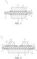
- FIG. 1 is a schematic view showing an example of a ceramic copper circuit board according to an embodiment.
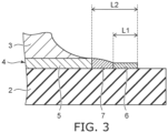
- FIG. 2 is a schematic view showing another example of the ceramic copper circuit board according to the embodiment.
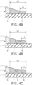
- FIG. 3 is a schematic view showing an example of a jutting part of the ceramic copper circuit board according to the embodiment.
- reference numeral 1 is a ceramic copper circuit board;
- reference numeral 2 is a ceramic substrate;
- reference numeral 3 is a copper circuit part;
- reference numeral 4 is a brazing material layer;
- reference numeral 5 is a bonding part;
- reference numeral 6 is a first jutting part;
- reference numeral 7 is a second jutting part; and
- reference numeral 8 is a copper heat dissipation plate.
- L1 is the length of the first jutting part 6; and
- L2 is the length of the entire jutting part.
- the ceramic copper circuit board 1 has a structure in which the copper circuit part 3 is bonded to at least one surface of the ceramic substrate 2 via the brazing material layer 4. As shown in FIG. 1 , the copper circuit part 3 may be bonded to one surface of the ceramic substrate 2; and the copper heat dissipation plate 8 may be bonded to another surface of the ceramic substrate 2. As shown in FIG. 2 , multiple copper circuit parts 3 may be bonded to one surface of the ceramic substrate 2. The copper circuit part 3 may be provided instead of the copper heat dissipation plate 8.
- the ceramic substrate 2 examples include a silicon nitride substrate, an aluminum nitride substrate, an aluminum oxide substrate, a zirconium oxide substrate, etc. It is favorable for the ceramic substrate 2 to be one of a silicon nitride substrate or an aluminum nitride substrate.
- the silicon nitride substrate and the aluminum nitride substrate are nitride ceramic substrates. As described below, a titanium nitride layer can be formed at the nitride ceramic substrate by active metal bonding.
- the aluminum oxide substrate and the zirconium oxide substrate are oxide ceramic substrates.
- a titanium oxide layer can be formed at the oxide ceramic substrate by active metal bonding. Comparing the nitride ceramic substrate and the oxide ceramic substrate, the nitride ceramic substrate has a higher thermal conductivity. In this respect, it is favorable to use the nitride ceramic substrate.
- the thickness of the ceramic substrate 2 is favorable for the thickness of the ceramic substrate 2 to be not less than 0.1 mm and not more than 3 mm.
- the strength may be reduced when the substrate thickness is less than 0.1 mm.
- the ceramic substrate may become a thermal resistor and may degrade the heat dissipation of the bonded body. It is therefore favorable for the thickness of the ceramic substrate 2 to be not less than 0.1 mm and not more than 3 mm, or even not less than 0.2 mm and not more than 1 mm.
- the three-point bending strength of the silicon nitride substrate is favorable for the three-point bending strength of the silicon nitride substrate to be not less than 600 MPa. It is favorable for the thermal conductivity of the silicon nitride substrate to be not less than 80 W/m ⁇ K.
- the substrate thickness can be reduced by increasing the strength of the silicon nitride substrate. It is therefore favorable for the three-point bending strength of the silicon nitride substrate to be not less than 600 MPa, or even not less than 700 MPa.
- the substrate thickness of the silicon nitride substrate can be thin, i.e., not more than 0.40 mm or even not more than 0.30 mm.
- the three-point bending strength of the aluminum nitride substrate is about 300 to 450 MPa.
- the thermal conductivity of the aluminum nitride substrate is not less than 160 W/m K. Because the strength of the aluminum nitride substrate is low, it is favorable for the substrate thickness to be not less than 0.60 mm.
- the copper circuit part 3 and the copper heat dissipation plate 8 can include copper plates or copper alloy plates. It is favorable for the copper circuit part 3 and the copper heat dissipation plate 8 to be made of oxygen-free copper. Oxygen-free copper is copper having a copper purity of not less than 99.96 wt% as indicated in JIS-H-3100 (ISO 1337, etc.). By making the copper circuit part 3 and the copper heat dissipation plate 8 thick, the current-carrying capacity and the heat dissipation can be improved. It is therefore favorable for the thicknesses of the copper circuit part 3 and the copper heat dissipation plate 8 to be not less than 0.1 mm, or even not less than 0.6 mm. More favorably, the thicknesses of the copper circuit part 3 and the copper heat dissipation plate 8 are not less than 0.8 mm.
- the copper circuit part 3 and the copper heat dissipation plate 8 each are bonded to the ceramic substrate 2 via the brazing material layers 4.
- the brazing material layer 4 includes the bonding part 5.
- the bonding part 5 is located between the ceramic substrate 2 and the copper circuit part 3 or between the ceramic substrate 2 and the copper heat dissipation plate 8.
- the brazing material layer 4 further includes a jutting part located at the periphery of the bonding part 5 in an in-plane direction.
- the in-plane direction is a direction parallel to the surface of the ceramic substrate 2.
- the brazing material layer 4 is located at the surface of the ceramic substrate 2.
- the jutting part juts along the in-plane direction from the edge of the copper circuit part 3 or the copper heat dissipation plate 8.
- the jutting part includes the first jutting part 6.
- the titanium content in the first jutting part 6 is within the range of not less than 70 mass% and not more than 100 mass%. It is favorable for the total of the titanium content and the nitrogen content in the first jutting part 6 to be within the range of not less than 90 mass% and not more than 100 mass%.
- the jutting part may further include the second jutting part 7.
- the second jutting part 7 is located between the bonding part 5 and the first jutting part 6.
- the titanium content in the second jutting part 7 is less than 70 mass%.
- the brazing material layer 4 has a structure in which the bonding part 5, the second jutting part 7, and the first jutting part 6 are connected to each other.
- the first jutting part 6 is positioned outward of the jutting part.
- the second jutting part 7 is positioned inward of the jutting part.
- the boundary between the bonding part 5 and the jutting part is referenced to the edge of the copper circuit part 3 or the copper heat dissipation plate 8 as shown in FIG. 3 .
- a line perpendicular to the surface of the ceramic substrate 2 is drawn from the edge of the copper circuit part 3 or the copper heat dissipation plate 8.
- the part that juts from the perpendicular line is the jutting part.
- the brazing material layer jutting part also is called simply the jutting part.
- Scanning electron microscope-energy dispersive X-ray spectrometry (SEM-EDX) is used to measure the titanium content of the jutting part.
- Area analysis of the jutting part is performed at any cross section of the ceramic copper circuit board 1. In the area analysis, the measurement area is set so that the entire jutting part is the analysis object.
- the entire jutting part refers to the part of the brazing material layer 4 other than the bonding part 5, and is the entire part jutting from the boundary between the ceramic substrate 2 and the jutting part.
- a titanium nitride layer is formed at the surface of the silicon nitride substrate.
- the boundary between the silicon nitride substrate and the titanium nitride layer is the boundary between the ceramic substrate 2 and the brazing material layer 4. That is, the titanium nitride layer is a portion of the bonding part 5 and a portion of the jutting part. Therefore, in the area analysis, care is taken that the titanium nitride layer is included in the measurement area; and the silicon nitride substrate is not included in the measurement area.
- a titanium oxide layer is formed at the surface of the oxide ceramic substrate.
- the boundary between the oxide ceramic substrate and the titanium oxide layer is the boundary between the ceramic substrate 2 and the brazing material layer 4. In the area analysis, care is taken that the titanium oxide layer is included in the measurement area; and the oxide ceramic substrate is not included in the measurement area.
- FE-SEM Field Emission SEM
- EDX is also called EDS.
- JSM-7200F made by JEOL Ltd., or a device having equivalent performance is used in FE-SEM.
- EX-74600U4L2Q made by JEOL Ltd., or a device having equivalent performance is used in EDX.
- the thickness direction is a direction perpendicular to the surface of the ceramic substrate 2.
- the width direction is a direction parallel to the cross section and the in-plane direction.
- the EDX measurement conditions are set to 50 scans with a measurement speed of 0.2 ms/bit. When performing the EDX area analysis, 256 ⁇ 198 imaged pixels, a detection count 3,700 to 4,100 cps (Count Per Second), and a quantitative map of 5 ⁇ 5 bit/point are set.
- the area analysis also is called surface analysis.
- EDX it is effective to use qualitative analysis using EDX to check the elements included in the brazing material layer beforehand to perform the area analysis after clarifying the elements to be designated.
- the total of the metal components, silicon, nitrogen, and carbon is set to 100 mass%.
- the total of the metal components, oxygen, and carbon is set to 100 mass%.
- the metal components are included in the measurement object when the metal components are not less than 0.01 mass%. This is because being less than 0.01 mass% is below the EDX detection limit.
- silicon and nitrogen diffuse into the brazing material layer. Therefore, silicon and nitrogen are included in the measurement object.
- Al and nitrogen are included in the measurement object for an aluminum nitride substrate.
- Al and oxygen are included in the measurement object for an aluminum oxide substrate.
- Zr and oxygen are included in the measurement object for zirconium oxide. Al and Zr are included in the measurement object as types of metal components.
- the first jutting part 6 is a region in which the titanium content is not less than 70 mass% and not more than 100 mass%.
- the tip of the jutting part may include only titanium or titanium nitride. It is favorable for the first jutting part 6 to be a region in which the total of the titanium content and the nitrogen content is not less than 90 mass% and not more than 100 mass%.
- the titanium nitride amount of the first jutting part 6 the titanium nitride amount is counted by considering all of the nitrogen detected by EDX to be included in titanium nitride (TiN).
- the tip of the jutting part may include only titanium or titanium oxide. It is favorable for the first jutting part 6 to be a region in which the total of the titanium content and the oxygen content is not less than 90 mass% and not more than 100 mass%. For the titanium oxide amount of the first jutting part 6, the titanium oxide amount is counted by considering all of the oxygen detected by EDX to be included in titanium oxide (TiO 2 ).
- the titanium nitride of the jutting part can be read as titanium oxide.
- the brazing material layer 4 includes one or two selected from Cu (copper), Ti (titanium), Sn (tin), and In (indium).
- examples of components of the first jutting part 6 other than titanium and nitrogen include Cu, Sn, and In. When much of these components remained, migration easily occurred between the copper circuit parts 3 adjacent to each other when the distance between the copper circuit parts was reduced.
- Migration is a phenomenon in which ionized metal moves between electrodes due to a voltage application when the circuit board is placed in an environment of high humidity, and a short-circuit occurs.
- the migration due to the ionized metal is called ion migration.
- semiconductor devices have been used in various industrial devices. For example, there are also cases where an electric vehicle is used in an environment of high moisture.
- active metal bonding Ag, Cu, Sn, In, Ti, etc., are used as the bonding brazing material.
- Ti has a low ionization tendency, and is resistant to moisture.
- Ti reacts with the nitride ceramic substrate to form titanium nitride. The formation of titanium nitride can suppress the occurrence of migration.
- the titanium content of the first jutting part 6 is within the range of not less than 70 mass% and not more than 100 mass%. Furthermore, it is favorable for the total of the titanium content and the nitrogen content of the first jutting part 6 to be not less than 90 mass% and not more than 100 mass%, or even not less than 99 mass% and not more than 100 mass%.
- the titanium content of the second jutting part 7 is less than 70 mass%.
- the second jutting part 7 includes not less than 30 mass% of components other than titanium.
- the titanium (or titanium nitride) included in the first jutting part 6 As described above, migration is suppressed by increasing the titanium (or titanium nitride) included in the first jutting part 6. On the other hand, when the titanium (or titanium nitride) is increased too much, the stress relaxation effect at the edge vicinity of the copper circuit part 3 or the copper heat dissipation plate 8 is reduced. It is therefore effective for the titanium content of the second jutting part 7 to be less than 70 mass%.
- the Cu content is not less than 5 mass and not more than 60 mass%, for the content of Sn or In to be not less than 5 mass% and not more than 45 mass%, and for the total content of Ti and titanium nitride to be not less than 10 mass% but less than 90 mass%.
- the presence of a prescribed amount of one or two selected from Cu, Sn, and In can improve the stress relaxation effect at the edge vicinity of the copper circuit part 3.
- the brazing material layer 4 includes one or two selected from Cu, Ti, Sn, and In. It is favorable for the Ag content of the brazing material layer 4 to be not less than 0 mass% and not more than 10 mass%.
- the brazing material layer 4 may include components other than Cu, Ti, Sn, and In.
- the Ag amount in the brazing material layer 4 is high, it may be difficult to form the first jutting part 6. It is therefore favorable for the Ag amount in the brazing material layer 4 to be not more than 10 mass%. More favorably, the Ag amount in the brazing material layer 4 is 0 mass%; and the brazing material layer 4 does not include Ag.
- the Ag amount being 0 mass% refers to being below the EDX detection limit (less than 0.01 mass%).
- the brazing material layer 4 may include not more than 10 mass% of metallic elements other than Cu, Ti, Sn, and In.
- metallic elements other than Cu, Ti, Sn, and In include one, two, or more selected from carbon, magnesium, molybdenum, tungsten, and rhenium.
- the brazing material layer 4 may include these elements as long as the total of these elements is not more than 10 mass%.
- the Cu content (mass%) of the bonding part 5 is taken as C1 .
- the Cu content (mass%) of the second jutting part 7 is taken as C2 .
- the stress relaxation effect can be improved.
- the mass ratio C2 / C1 is greater than 0.7, the difference between the Cu amount of the second jutting part 7 and the Cu amount of the first jutting part 6 may become too large, and the stress relaxation effect may decrease.
- the lower limit of the mass ratio C2 / C1 is not particularly limited, it is favorable for the lower limit to be not less than 0.1.
- the mass ratio C2 / C1 is less than 0.1, the Cu amount of the second jutting part 7 may be too low, and the stress relaxation effect may decrease. It is therefore favorable for the mass ratio C2 / C1 to be not less than 0.1 and not more than 0.7, or even not less than 0.2 and not more than 0.5.
- the area analysis of SEM-EDX described above is used to measure the Cu amount of the bonding part 5, the Cu amount of the first jutting part 6, and the Cu amount of the second jutting part 7.
- the brazing material layer 4 is divided into the bonding part 5 and the jutting part according to the position of the edge of the copper circuit part 3 or the copper heat dissipation plate 8.
- the jutting part is divided into the region of the first jutting part 6 and the region of the second jutting part 7 according to the Ti amount.
- the average value of the Cu amount of the bonding part 5 is used as the Cu amount of the bonding part 5.
- the average value of the Cu amount in the region of the first jutting part 6 is used as the Cu amount of the first jutting part 6.
- the average value of the Cu amount in the region of the second jutting part is used as the Cu amount of the second jutting part 7.
- the first jutting part 6, and the second jutting part 7, five measurement areas are analyzed with EDX; and the Cu amounts of the bonding part 5, the first jutting part 6, and the second jutting part 7 included in each measurement area are measured.
- the average value of the Cu amounts of the five measurement areas are calculated, and the obtained average values are used respectively as the Cu amounts of the parts.
- the five measurement areas are obtained from five mutually-different cross sections. Multiple cross sections that pass respectively through multiple sides of the copper circuit part 3 of the ceramic copper circuit board 1 may be obtained, or multiple cross sections may be obtained from one side.
- the Ti content (mass%) of the bonding part 5 is taken as C3 .
- the Ti content (mass%) of the second jutting part 7 is taken as C4. It is favorable for the mass ratio C4 / C3 to be not more than 1.2. By setting the mass ratio C4 / C3 to be not more than 1.2, a gradient can be provided to the composition of the Ti amount from the bonding part 5 toward the second jutting part 7.
- the mass ratio C4 / C3 being greater than 1.2 means that there is less Cu, Sn, etc., in the second jutting part 7. Although not particularly limited, it is favorable for the lower limit of the mass ratio C4 / C3 to be greater than 1. It is therefore favorable for the mass ratio C4 / C3 to be greater than 1 and not more than 1.2.
- the SEM-EDX area analysis described above is used to measure the Ti amounts of the bonding part 5 and the second jutting part 7.
- the average value of the Ti amount in the region of the second jutting part 7 is used as the Ti amount of the second jutting part 7.
- the average value of the Ti amount in the region 100 ⁇ m inward from the boundary between the bonding part 5 and the jutting part is used as the Ti amount of the bonding part 5.
- the Ti amounts of the bonding part 5 and the second jutting part 7 are analyzed by EDX; and the Ti amounts of the bonding part 5 and the second jutting part 7 included in each measurement area are measured. For each of the bonding part 5 and the second jutting part 7, the average values of the Ti amounts of the five measurement areas are calculated, and the obtained average values are used respectively as the Ti amounts of the parts.
- the five measurement areas are obtained from five mutually-different cross sections. Multiple cross sections that pass respectively through multiple sides of the copper circuit part of the ceramic copper circuit board may be obtained, or multiple cross sections may be obtained from one side. The five cross sections that are used to measure the Cu amount may be used to measure the Ti amount together with the Cu amount.
- the length of the first jutting part 6 in the direction from the bonding part 5 toward the first jutting part 6 is taken as L1 .
- the length of the entire jutting part in this direction is taken as L2.
- Length L2 - length L1 corresponds to the length of the second jutting part 7.
- the characteristics of the first and second jutting parts 6 and 7 can be further improved by controlling the length of the first jutting part 6 and the length of the second jutting part 7.
- Ag migration can be suppressed by not including Ag in the bonding part 5 and the brazing material layer jutting part.
- An active metal brazing material is used to bond the ceramic substrate 2 and the copper circuit part 3.
- the active metal brazing material includes metals such as Ag, Cu, Ti, Sn, In, etc.; however, in the active metal brazing material, Ag is the element most prone to migration. Ag migration can be suppressed by reducing the Ag content or by not including Ag.
- the SEM-EDX area analysis described above is utilized to measure the length ( L1 ) of the first jutting part 6 and the length ( L2 - L1 ) of the second jutting part 7.
- the region of the jutting part upper surface in which the titanium content is not less than 70 mass% is designated based on the result of the area analysis.
- the region of the designated region that is continuous with the jutting part tip is extracted.
- the jutting part tip is the location most distant to the bonding part 5 at which the ceramic substrate 2 and the first jutting part 6 are in contact.
- the location in the extracted region most proximate to the copper circuit part 3 is designated.
- a line is drawn perpendicular to the surface of the ceramic substrate 2 from the location most proximate to the copper plate.
- the length from the jutting part tip to the perpendicular line is taken as the length L1 of the first jutting part 6.
- the length ( L2 - L1 ) of the length L1 of the first jutting part 6 subtracted from the length L2 of the entire jutting part is taken as the length of the second jutting part 7.
- the length L1 of the first jutting part is determined using the region continuous with the jutting part tip.
- FIGS. 4A to 4C are schematic views showing lengths of the first jutting part and lengths of the entire jutting part.
- reference numeral 6 is the first jutting part; and reference numeral 7 is the second jutting part.
- the first jutting part 6 is present at the tip of the jutting part.
- the region in which the titanium content is not less than 70 mass% is one lump.
- the length L1 is measured by designating the location of the first jutting part 6 at the jutting part upper surface most proximate to the copper circuit part 3.
- the second jutting part 7 is present between a portion and another portion of the first jutting part 6 at the upper surface of the jutting part.
- the length to the jutting part tip from the boundary between the second jutting part 7 and the portion of the first jutting part 6 continuous with the jutting part tip at the upper surface of the jutting part is used as the length L1.
- first jutting parts 6 that are separated from each other are present at the upper surface of the jutting part.
- the second jutting part 7 is present between the first jutting parts 6.
- the length to the jutting part tip from the boundary between the second jutting part 7 and one first jutting part 6 continuous with the jutting part tip at the upper surface of the jutting part is used as the length L1.
- the bonding part 5 may include carbon.
- the bonding part 5 including carbon means that the bonding brazing material includes carbon.
- the fluidity of the brazing material can be controlled by the bonding brazing material including carbon.
- the bonding brazing material paste can be uniformly coated.
- the bonding part 5 includes carbon
- the first jutting part 6 or the second jutting part 7 also may include carbon.
- the carbon content of the bonding part 5 is within the range of not less than 0.01 mass% and not more than 2 mass%. More favorably, the carbon content of the bonding part 5 is within the range of not less than 0.05 mass% and not more than 1 mass%. It is favorable for the carbon content of the first or second jutting part 6 or 7 also to be not less than 0 mass% and not more than 1 mass%.
- FIG. 5 is a conceptual view illustrating the method for measuring the inclination angle of the copper circuit part side surface.
- reference numeral 3 is the copper circuit part; reference numeral 6 is the first jutting part; and reference numeral 7 is the second jutting part.
- a point A is the intersection between the brazing material layer 4 and the edge of the copper circuit part 3.
- a point B is the midpoint of the side surface of the copper circuit part 3 in the thickness direction.
- a point C is the intersection between the horizontal line from the point A and the perpendicular line from the point B.
- a SEM photograph of any cross section of the ceramic copper circuit board 1 is used to measure the inclination angle ⁇ .
- a SEM photograph from when the jutting part was analyzed by SEM-EDX may be used.
- the point A which is the intersection between the brazing material layer 4 and the edge of the copper circuit part 3, and the point B, which is the midpoint of the side surface of the copper circuit part 3 in the thickness direction, are set in the cross-sectional photograph.
- the point C which is the intersection of the horizontal line from the point A and the perpendicular line from the point B, is set.
- a right triangle bounded by the three points ABC is generated.
- the angle between side BC and side AB is used as the inclination angle ⁇ of the side surface of the copper circuit part 3.
- the inclination angle ⁇ of the side surface of the copper circuit part 3 also may be called simply the inclination angle ⁇ .
- the stress at the bonding end portion can be relaxed by setting the inclination angle ⁇ to be within the range of not less than 30° and not more than 70°.
- the inclination angle is less than 30°, the inclined surface of the copper circuit part 3 may lengthen, and the area for mounting the semiconductor element may be reduced.
- the inclination angle ⁇ is greater than 70°, the stress relaxation effect of the bonding end portion may be insufficient. It is therefore favorable for the inclination angle ⁇ to be within the range of not less than 30° and not more than 70°, or even not less than 40° and not more than 60°.
- the multiple copper circuit parts 3 may be bonded to at least one surface of the ceramic substrate 2.
- the shortest distance between the adjacent copper circuit parts 3 may be within the range of not less than 0.2 mm and not more than 2 mm.
- FIG. 6 is a schematic view showing an example of a semiconductor device according to an embodiment.
- reference numeral 9 is a semiconductor element; and reference numeral 10 is a semiconductor device. Otherwise, the reference numerals are the same as the reference numerals of FIG. 1 .
- P is the shortest distance between the adjacent copper circuit parts 3.
- the shortest distance between the adjacent copper circuit parts 3 also is called the pitch.
- the pitch P is the pitch P. In other words, the distance between the intersection between the brazing material layer jutting part and the edge of the copper circuit part 3 is the pitch P.
- the pitch P being within the range of not less than 0.2 mm and not more than 2 mm means that the distance between the adjacent copper circuit parts 3 is short.
- the bonding area of the copper circuit part 3 can be increased by reducing the distance between the adjacent copper circuit parts 3. That is, the mounting area of the semiconductor element 9, etc., can be increased.
- the size of the ceramic copper circuit board 1 can be reduced. That is, the ceramic copper circuit board 1 can be smaller without reducing the mounting area of the semiconductor element 9, etc.
- the pitch P may not be within the range of not less than 0.2 mm and not more than 2 mm.
- the effects described above can be obtained when the pitch P is within the range of not less than 0.2 mm and not more than 2 mm.
- the shortest distance between one copper circuit part 3 and another copper circuit part 3 adjacent to the one copper circuit part 3 is within the range of not less than 0.2 mm and not more than 2 mm.
- the shortest distance between the other copper circuit part 3 and yet another copper circuit part 3 adjacent to the other copper circuit part 3 is within the range of not less than 0.2 mm and not more than 2 mm.
- Such a ceramic copper circuit board 1 is applicable to the semiconductor device 10 to which the semiconductor element 9 is mounted.
- the semiconductor element 9 is mounted on the copper circuit part 3.
- one semiconductor element 9 is mounted.
- Multiple semiconductor elements 9 may be mounted respectively to multiple copper circuit parts 3.
- a leadframe or wire bonding may be included as necessary.
- a plating film, a mold resin, etc. may be provided at the surface of the copper circuit part 3 as necessary.
- the occurrence of migration can be suppressed. Furthermore, the occurrence of migration can be further suppressed by the pitch P being within the range of not less than 0.2 mm and not more than 2 mm, or by 1 ⁇ P / D ⁇ 3 being satisfied.
- a method for manufacturing the ceramic copper circuit board 1 according to the embodiment will now be described.
- the manufacturing method is not limited as long as the ceramic copper circuit board 1 according to the embodiment has the configuration described above.
- the following method is illustrated as an example to obtain the ceramic copper circuit board 1 with a high yield.
- the ceramic substrate 2 is prepared.
- the ceramic substrate 2 include a silicon nitride substrate, an aluminum nitride substrate, etc.
- a copper plate or a copper alloy plate can be used as the member for forming the copper circuit part 3 or the copper heat dissipation plate 8. It is favorable for the copper plate to be oxygen-free copper.
- Oxygen-free copper is copper that has a copper purity of not less than 99.96 wt% as indicated in JIS-H-3100. JIS-H-3100 (2016) corresponds to ISO 1337, etc.
- a bonding brazing material is prepared. It is favorable for the bonding brazing material to include not less than 50 mass% of Cu, not less than 4 mass% and not more than 30 mass% of Ti, not less than 5 mass% and not more than 45 mass% of one or two selected from Sn or In, and not less than 0 mass% and not more than 2 mass% of carbon. Ti may be added as titanium hydride (TiH 2 ). It is effective not to add Ag to the bonding brazing material.
- a bonding brazing material to which the active metal, Ti (including TiH 2 ), is added is an active metal brazing material.
- the Ti amount is favorably not less than 2 mass%, and more favorably not less than 5 mass%.
- the thermal bonding process is performed in a nitrogen atmosphere in the continuous furnace.
- the Ti amount in the active metal brazing material is increased, the Ti that contributes to the bonding can be ensured even when the Ti reacts with the nitrogen atmosphere.
- the average particle size D 50 of the Cu powder used as the raw material of the brazing material is not more than 12.0 ⁇ m, or even not more than 10.0 ⁇ m. It is favorable for the average particle size D 50 of the Ti powder or the TiH 2 powder to be not more than 6.0 ⁇ m, or even not more than 4.0 ⁇ m. It is favorable for the average particle size D 50 of the Sn powder or the In powder to be not more than 16.0 ⁇ m, or even not more than 14.0 ⁇ m. It is favorable for the average particle size D 50 of the carbon powder to be not more than 6.0 ⁇ m, or even not more than 4.0 ⁇ m. The reactions of the powders can be made uniform by controlling the particle sizes of the powders. Although Ag may be added to the raw material in a small amount, it is favorable not to add Ag.
- the average particle size D 50 of the Cu powder is less than the average particle size D 50 of the Sn powder or the In powder.
- one or two selected from Cu, Sn, and In is used as the base material of the brazing material composition.
- the melting point of Sn or In is less than the melting point of Cu.
- the reaction of the Cu powder with the Sn or In powder can be made homogeneous by controlling the Sn or In particle size.
- the average particle size D 50 of the metallic element powder is less than the average particle size D 50 of the Sn powder or the In powder.
- the metallic element other than Cu, Ti, Sn, and In include one, two, or more selected from carbon, magnesium, molybdenum, tungsten, rhenium, and cobalt. These elements may be added to the raw material as long as the total of these elements is not more than 10 mass%.
- a process of bonding the ceramic substrate 2 and the copper plate is performed using such a bonding brazing material.
- a brazing material paste is prepared by mixing the bonding brazing material with an organic substance.
- a brazing material paste layer is formed by coating the brazing material paste on the surface of the ceramic substrate 2 (or the copper plate).
- the copper plate (or the ceramic substrate 2) is placed on the brazing material paste layer.
- the stack of the ceramic substrate, the brazing material paste, and the copper plate is called an unbonded stacked body.
- the thermal bonding process is a technique in which the unbonded stacked body is placed in a storage container, and heat treatment is performed.
- the continuous technique is a technique in which the unbonded stacked body is placed on a belt conveyor, and heat treatment is performed while being moved.
- the batch technique is suited to a bonding process in a vacuum.
- the continuous technique is suited to a bonding process in a nitrogen atmosphere.
- a batch thermal bonding device also is called a batch furnace.
- a continuous thermal bonding device also is called a continuous furnace.
- the heating temperature In the batch technique, it is favorable for the heating temperature to be not less than 750 °C and not more than 850 °C, and the pressure to be a vacuum of not more than 10 -3 Pa. In the continuous technique, it is favorable for the heating temperature to be within the range of not less than 750 °C and not more than 950 °C.
- the thermal bonding process is performed in a nitrogen atmosphere.
- the nitrogen atmosphere is an atmosphere in which nitrogen is not less than 70 vol%. It is favorable for the nitrogen amount of the nitrogen atmosphere to be not less than 70 vol%, or even not less than 85 vol% and not more than 100 vol%.
- examples of the nitrogen atmosphere include an inert gas or ambient air.
- the thermal bonding process includes a temperature raising process, a holding process, and a temperature lowering process.
- the temperature raising process for example, the temperature rises from room temperature to the bonding temperature.
- the holding process is performed after the temperature raising process; and the bonding temperature is maintained.
- the temperature lowering process is performed after the holding process; and the temperature falls from the bonding temperature to, for example, room temperature.
- the temperature raising rate is set to be not less than 30 °C/min. Although not particularly limited, it is favorable for the upper limit of the temperature raising rate to be not more than 100 °C/min. When the temperature raising rate is greater than 100 °C/min, there is a possibility that the bondability may degrade. It is therefore favorable for the temperature raising rate to be not less than 30 °C/min and not more than 100 °C/min, or even not less than 40 °C/min and not more than 70 °C/min.
- the bonding temperature is not less than 750 °C. It is favorable for the upper limit of the bonding temperature to be not more than 1,000 °C. When the bonding temperature is greater than 1,000 °C, the bonding temperature approaches the melting point of copper (1,085 °C); and there is a possibility that the copper plate may deform. It is therefore favorable for the bonding temperature to be not less than 750 °C and not more than 1,000 °C, or even not less than 800 °C and not more than 950 °C.
- the bonding temperature is maintained for not less than 10 minutes.
- the holding time of the bonding temperature is called the heating holding time. It is favorable for the heating holding time to be not less than 10 minutes and not more than 100 minutes. When the heating holding time is less than 10 minutes, there is a possibility that the time may be insufficient for the brazing material to melt or solidify. When the heating holding time is greater than 100 minutes, there is a possibility that too much Sn or In may diffuse into the copper plate.
- the temperature lowering rate is set to be not less than 30 °C/min. Although not particularly limited, it is favorable for the upper limit of the temperature lowering rate to be not more than 100 °C/min. When the temperature lowering rate is greater than 100 °C/min, there is a possibility that the bondability may degrade. It is therefore favorable for the temperature lowering rate to be not less than 30 °C/min and not more than 100 °C/min, or even not less than 40 °C/min and not more than 70 °C/min.
- the difference between the temperature raising rate and the temperature lowering rate is not more than 20 °C/min. That is, it is favorable for
- a melting reaction and a solidification reaction are caused by heating the brazing material paste. These reactions occur in the temperature raising process and the temperature lowering process.
- the stress that occurs in the melting reaction and the solidification reaction can be homogenized by reducing the difference between the temperature raising rate and the temperature lowering rate. Discrepancies such as warp, etc., can be suppressed thereby.
- the thermal bonding process may be performed with a weight placed on the bonded body as necessary.
- An unbonded stacked body on which the thermal bonding process has been performed is called a bonded body.
- a pattern shape is provided in the copper plate by patterning by etching the obtained bonded body.
- the copper circuit part 3 is formed by providing the pattern shape in the copper plate.
- the ceramic copper circuit board 1 that includes the copper circuit part 3 is obtained.
- Multi-part manufacturing may be performed by scribing as necessary. Multi-part manufacturing is a method in which small bonded bodies are obtained by cutting a large bonded body. There is also a method of subdividing the bonded body or a method of subdividing the ceramic copper circuit board.
- the copper circuit part 3 and the copper heat dissipation plate 8 are formed by etching the copper plate.
- a portion of the brazing material layer 4 is exposed by etching the copper plate.
- a process of etching the brazing material layer 4 is performed. It is favorable for the process of etching the brazing material layer to be performed not less than two times.
- a chemical polishing process may be combined with the etching of the brazing material layer as necessary. The processing time can be shortened by combining chemical polishing with the etching of the brazing material layer.
- the titanium contents of the first and second jutting parts 6 and 7 can be controlled. Also, the length L1 of the first jutting part 6 and the length L2 of the entire jutting part can be controlled by adjusting the concentration of the etchant, the processing time of the etchant, etc.
- the titanium amount of the first jutting part 6, the length L1 of the first jutting part 6, etc. can be adjusted by using a resist.
- the resist is located, after the copper plate is etched, on the location of the jutting part at which the second jutting part is formed. Also, for example, when the process of etching the brazing material layer 4 is performed multiple times, there is a method in which the etching durations of the second and subsequent times are less than the etching duration of the first time.
- a method in which the side surface of the copper circuit part 3 is etched after the brazing material layer 4 is etched also is effective.
- the second jutting part 7 can be formed by etching the side surface of the copper circuit part 3.
- the first jutting part 6 may be provided by further etching the second jutting part 7 as necessary. By etching the second jutting part 7, the elements (e.g., copper) other than titanium included in the second jutting part 7 are removed; and the first jutting part 6 is formed.
- the elements e.g., copper
- the etchant for etching the side surface of the copper circuit part 3 can include an iron(III) chloride solution.
- a chemical polishing liquid may be used instead of the iron(III) chloride solution. It is favorable to use a chemical polishing liquid in which sulfuric acid and hydrogen peroxide are mixed as the chemical polishing liquid.
- An etching mask (a resist) is coated onto the surface of the copper circuit part 3 as necessary.
- the etching process of the brazing material layer 4 and an etching process for providing an incline in the side surface of the copper circuit part 3 may be combined. As described above, the brazing material layer 4 is easily etched in the etching process of the copper circuit part 3 by not including Ag in the brazing material layer 4.
- a semiconductor device is obtained by mounting a semiconductor element, etc., to the obtained ceramic copper circuit board.
- the ceramic substrates 2 shown in Table 1 and the copper plates shown in Table 2 were prepared. Oxygen-free copper plates were used for each of the copper plates.
- Bonding brazing material pastes were prepared using the bonding brazing materials; and the unbonded stacked bodies shown in Table 4 were made. Copper plates were placed at the two surfaces of the ceramic substrate 2.
- Ceramic substrate Copper plate Brazing material Unbonded stacked body 1 Silicon nitride substrate 1 Copper plate 1 Brazing material 1 Unbonded stacked body 2 Silicon nitride substrate 1 Copper plate 1 Brazing material 2 Unbonded stacked body 3 Silicon nitride substrate 1 Copper plate 3 Brazing material 3 Unbonded stacked body 4 Silicon nitride substrate 2 Copper plate 1 Brazing material 3 Unbonded stacked body 5 Silicon nitride substrate 2 Copper plate 2 Brazing material 4 Unbonded stacked body 6 Aluminium nitride substrate 1 Copper plate 3 Brazing material 3 Unbonded stacked body 7 Silicon nitride substrate 2 Copper plate 2 Brazing material 5
- bonded bodies were made by performing a thermal bonding process on the unbonded stacked bodies.
- a continuous furnace was used in the thermal bonding process.
- the heating holding temperature was set to be not less than 850 °C and not more than 950 °C; and the heating holding time was set to be not less than 30 minutes and not more than 60 minutes.
- the temperature raising rate and the temperature lowering rate were set to 20 to 100 °C/min.
- the difference between the temperature raising rate and the temperature lowering rate was set to be not more than 20 °C/min.
- the thermal bonding process was performed in a nitrogen atmosphere. Bonded bodies were obtained by the thermal bonding process. Bonded bodies 1 to 7 were obtained respectively from unbonded stacked bodies 1 to 7.
- Ceramic copper circuit boards according to the examples and the comparative examples were made by performing an etching process on the obtained bonded bodies.
- the configurations of the bonded bodies were as shown in Table 5.
- the methods for measuring the titanium amount, the total amount of titanium and nitrogen, the length L1, the length L2, and the inclination angle ⁇ were as described above.
- the ceramic copper circuit boards according to the examples included the first jutting part 6 and the second jutting part 7.
- Cu was within the range of not less than 5 mass and not more than 60 mass%; and Sn was within the range of not less than 5 mass% and not more than 45 mass%.
- the ceramic copper circuit boards according to the comparative examples did not include the first jutting part 6.
- the titanium amount of the first jutting part 6 was not less than 70 mass%; and the titanium amount of the second jutting part 7 was less than 70 mass%.
- the Cu amount C1 (mass%) of the bonding part 5 and the Cu amount C2 (mass%) of the second jutting part 7 were compared.
- the Ti amount C3 (mass%) of the bonding part 5 and the Ti amount C4 (mass%) of the second jutting part 7 were compared.
- the Ti amount (mass%) was the amount (mass%) of the total of titanium and titanium nitride.
- the shortest distance (the pitch) P between the adjacent copper circuit parts 3 and pitch P/copper circuit part thickness D were measured. The results are shown in Table 6.
- TCT test heat resistance cycle test
- migration test migration test
- one cycle was -50 °C ⁇ 30 minutes -> 25 °C ⁇ 10 minutes -> 155 °C ⁇ 30 minutes -> 25 °C ⁇ 10 minutes.
- silicon nitride substrates the presence or absence of discrepancies after 2,000 cycles was checked.
- aluminum nitride substrates the presence or absence of discrepancies after 500 cycles was checked.
- a discrepancy is the occurrence of a crack in the brazing material layer or the ceramic substrate.
- the presence or absence of discrepancies was checked using ultrasonic testing. The tests were performed for one hundred ceramic copper circuit boards for each example and comparative example; and the occurrence rates (%) of the discrepancy were checked.
- the measurement environment was set to 85 °C and a humidity of 85%; and the ceramic copper circuit board was left for 2,000 hours with a DC voltage of 1,000 V applied between the front and back surfaces of the ceramic copper circuit board in which a pattern was formed. After this time, the ceramic copper circuit board was dried at 120 °C ⁇ 2 hours, and then the insulation resistance value between the copper circuit part 3 at the front side and the copper heat dissipation plate 8 at the backside and the insulation resistance value between the adjacent copper circuit parts 3 at the front side were measured.
- Bonded bodies for which the change rate of the insulation resistance values before and after the test was not more than 10% were taken to be good. Bonded bodies for which the change rate was not less than 11% were taken to be defective.
- the determination was performed by change rate (%) [(insulation resistance value after testing - insulation resistance value before testing)/insulation resistance value before testing] ⁇ 100. The tests were performed, and the defect occurrence rate (%) was checked for each set of one hundred ceramic copper circuit boards.
- the insulation resistance value between the copper circuit part 3 at the front side and the copper heat dissipation plate 8 at the backside was measured for fifty ceramic copper circuit boards; and the insulation resistance value between the adjacent copper circuit parts 3 at the front side was measured for the other fifty ceramic copper circuit boards.
- wire bonding or copper tape between copper circuit patterns at the front side was provided as necessary to prepare the copper circuit patterns to have the same potential.
- the TCT characteristics of the ceramic copper circuit boards according to the comparative examples 1 and 2 were equivalent to the TCT characteristics of the ceramic copper circuit boards according to the examples.
- the migration characteristics of the ceramic copper circuit boards according to the comparative examples 1 and 2 degraded compared to the migration characteristics of the ceramic copper circuit boards according to the examples. Therefore, it can be seen that the inclusion of the first and second jutting parts was effective to further improve the migration characteristics while improving the TCT characteristics.
- Embodiments may include the following features.
- a ceramic copper circuit board comprising:
- a total of the titanium content and a nitrogen content of the first jutting part is within a range of not less than 90 mass% and not more than 100 mass%.
- brazing material layer further includes carbon
- the ceramic copper circuit board according to any one of Features 1 to 11, wherein the ceramic substrate is a silicon nitride substrate.
- the ceramic copper circuit board according to any one of Features 1 to 12, wherein a thickness of the copper circuit part is not less than 0.6 mm.
- a semiconductor device comprising:
Landscapes
- Engineering & Computer Science (AREA)
- Microelectronics & Electronic Packaging (AREA)
- Chemical & Material Sciences (AREA)
- Ceramic Engineering (AREA)
- Manufacturing & Machinery (AREA)
- Inorganic Chemistry (AREA)
- Materials Engineering (AREA)
- Structural Engineering (AREA)
- Organic Chemistry (AREA)
- Ceramic Products (AREA)
- Manufacturing Of Printed Wiring (AREA)
Abstract
Description
- Embodiments described below are related to a ceramic copper circuit board and a semiconductor device using a ceramic copper circuit board.
- In recent years, power modules are being used in electric vehicles, electric trains, and the like to control large currents and high voltages due to the higher performance of industrial devices and global environmental issues. The heat generated from semiconductor elements mounted in such power modules also continues to increase. Therefore, heat dissipation is important for circuit boards for power modules. Ceramic-metal bonded circuit boards in which a metal plate of copper, aluminum, or the like is bonded to a ceramic substrate having high thermal conductivity are widely used. Also, active metal bonding that utilizes a brazing material is widely used as a method to bond the ceramic substrate and the copper plate. Brazing materials used in active metal bonding are called active metal brazing materials.
- For example,
Japanese Patent No. 6158144 Patent Literature 1, a brazing material layer jutting part is formed at the ceramic circuit board. According toPatent Literature 1, TCT characteristics are improved by forming the brazing material layer jutting part. As inPatent Literature 1, a bonding method that uses a brazing material layer including Ag, Cu, and Ti is called active metal bonding. Generally, in active metal bonding, an active metal is included in the brazing material; and it is common to use Ag, Cu, and Ti as the bonding brazing material. Among the bonding brazing materials, Ag is an expensive element. - For example,
JP-A 2003-283064 Patent Literature 2 does not include Ag in the brazing material. Therefore, the etchability of the brazing material layer was good.Patent Literature 2 discusses an active metal brazing material that does not include Ag. -
- Patent Literature 1:
Japanese Patent No. 6158144 - Patent Literature 2:
JP-A 2003-283064 - In
Patent Literature 2, the etchability of the brazing material layer is improved. On the other hand, a brazing material layer jutting part such as that ofPatent Literature 1 could not be formed. Because the brazing material layer jutting part could not be formed, a problem occurred in which the TCT characteristics of the ceramic circuit board degraded. - A ceramic copper circuit board according to an embodiment controls the brazing material layer jutting part of a ceramic copper circuit board that uses a brazing material layer not including Ag.
- A ceramic copper circuit board according to an embodiment includes a ceramic substrate, and a copper circuit part bonded to at least one surface of the ceramic substrate via a brazing material layer. The brazing material layer includes one or two selected from Cu, Ti, Sn, or In. The brazing material layer includes a bonding part located between the ceramic substrate and the copper circuit part, and a first jutting part located at a periphery of the bonding part; and a titanium content of the first jutting part is within a range of not less than 70 mass% and not more than 100 mass%.
-
- [
FIG. 1 ]
FIG. 1 is a schematic view showing an example of a ceramic copper circuit board according to an embodiment. - [
FIG. 2 ]
FIG. 2 is a schematic view showing another example of the ceramic copper circuit board according to the embodiment. - [
FIG. 3 ]
FIG. 3 is a schematic view showing an example of a jutting part of the ceramic copper circuit board according to the embodiment. - [
FIG. 4 ]
FIG. 4 is a schematic view showing the length of the first jutting part and the length of the entire jutting part. - [
FIG. 5 ]
FIG. 5 is a conceptual view illustrating a method for measuring an inclination angle of a copper circuit part side surface. - [
FIG. 6 ]
FIG. 6 is a schematic view showing an example of a semiconductor device according to an embodiment. - A ceramic copper circuit board according to an embodiment includes a ceramic substrate, and a copper circuit part bonded to at least one surface of the ceramic substrate via a brazing material layer. The brazing material layer includes one or two selected from Cu, Ti, Sn, or In. The brazing material layer includes a bonding part located between the ceramic substrate and the copper circuit part, and a first jutting part located at a periphery of the bonding part; and a titanium content of the first jutting part is within a range of not less than 70 mass% and not more than 100 mass%.
-
FIG. 1 is a schematic view showing an example of a ceramic copper circuit board according to an embodiment.FIG. 2 is a schematic view showing another example of the ceramic copper circuit board according to the embodiment.FIG. 3 is a schematic view showing an example of a jutting part of the ceramic copper circuit board according to the embodiment. InFIGS. 1 to 3 ,reference numeral 1 is a ceramic copper circuit board;reference numeral 2 is a ceramic substrate;reference numeral 3 is a copper circuit part;reference numeral 4 is a brazing material layer;reference numeral 5 is a bonding part;reference numeral 6 is a first jutting part;reference numeral 7 is a second jutting part; andreference numeral 8 is a copper heat dissipation plate. L1 is the length of the first juttingpart 6; and L2 is the length of the entire jutting part. - The ceramic
copper circuit board 1 according to the embodiment has a structure in which thecopper circuit part 3 is bonded to at least one surface of theceramic substrate 2 via thebrazing material layer 4. As shown inFIG. 1 , thecopper circuit part 3 may be bonded to one surface of theceramic substrate 2; and the copperheat dissipation plate 8 may be bonded to another surface of theceramic substrate 2. As shown inFIG. 2 , multiplecopper circuit parts 3 may be bonded to one surface of theceramic substrate 2. Thecopper circuit part 3 may be provided instead of the copperheat dissipation plate 8. - Examples of the
ceramic substrate 2 include a silicon nitride substrate, an aluminum nitride substrate, an aluminum oxide substrate, a zirconium oxide substrate, etc. It is favorable for theceramic substrate 2 to be one of a silicon nitride substrate or an aluminum nitride substrate. The silicon nitride substrate and the aluminum nitride substrate are nitride ceramic substrates. As described below, a titanium nitride layer can be formed at the nitride ceramic substrate by active metal bonding. - The aluminum oxide substrate and the zirconium oxide substrate are oxide ceramic substrates. A titanium oxide layer can be formed at the oxide ceramic substrate by active metal bonding. Comparing the nitride ceramic substrate and the oxide ceramic substrate, the nitride ceramic substrate has a higher thermal conductivity. In this respect, it is favorable to use the nitride ceramic substrate.
- It is favorable for the thickness of the
ceramic substrate 2 to be not less than 0.1 mm and not more than 3 mm. The strength may be reduced when the substrate thickness is less than 0.1 mm. When the substrate thickness is greater than 3 mm, the ceramic substrate may become a thermal resistor and may degrade the heat dissipation of the bonded body. It is therefore favorable for the thickness of theceramic substrate 2 to be not less than 0.1 mm and not more than 3 mm, or even not less than 0.2 mm and not more than 1 mm. - It is favorable for the three-point bending strength of the silicon nitride substrate to be not less than 600 MPa. It is favorable for the thermal conductivity of the silicon nitride substrate to be not less than 80 W/m·K. The substrate thickness can be reduced by increasing the strength of the silicon nitride substrate. It is therefore favorable for the three-point bending strength of the silicon nitride substrate to be not less than 600 MPa, or even not less than 700 MPa. The substrate thickness of the silicon nitride substrate can be thin, i.e., not more than 0.40 mm or even not more than 0.30 mm.
- The three-point bending strength of the aluminum nitride substrate is about 300 to 450 MPa. On the other hand, the thermal conductivity of the aluminum nitride substrate is not less than 160 W/m K. Because the strength of the aluminum nitride substrate is low, it is favorable for the substrate thickness to be not less than 0.60 mm.
- The
copper circuit part 3 and the copperheat dissipation plate 8 can include copper plates or copper alloy plates. It is favorable for thecopper circuit part 3 and the copperheat dissipation plate 8 to be made of oxygen-free copper. Oxygen-free copper is copper having a copper purity of not less than 99.96 wt% as indicated in JIS-H-3100 (ISO 1337, etc.). By making thecopper circuit part 3 and the copperheat dissipation plate 8 thick, the current-carrying capacity and the heat dissipation can be improved. It is therefore favorable for the thicknesses of thecopper circuit part 3 and the copperheat dissipation plate 8 to be not less than 0.1 mm, or even not less than 0.6 mm. More favorably, the thicknesses of thecopper circuit part 3 and the copperheat dissipation plate 8 are not less than 0.8 mm. - The
copper circuit part 3 and the copperheat dissipation plate 8 each are bonded to theceramic substrate 2 via the brazing material layers 4. Thebrazing material layer 4 includes thebonding part 5. Thebonding part 5 is located between theceramic substrate 2 and thecopper circuit part 3 or between theceramic substrate 2 and the copperheat dissipation plate 8. Thebrazing material layer 4 further includes a jutting part located at the periphery of thebonding part 5 in an in-plane direction. The in-plane direction is a direction parallel to the surface of theceramic substrate 2. Thebrazing material layer 4 is located at the surface of theceramic substrate 2. The jutting part juts along the in-plane direction from the edge of thecopper circuit part 3 or the copperheat dissipation plate 8. - As shown in
FIG. 1 , the jutting part includes the first juttingpart 6. The titanium content in the first juttingpart 6 is within the range of not less than 70 mass% and not more than 100 mass%. It is favorable for the total of the titanium content and the nitrogen content in the first juttingpart 6 to be within the range of not less than 90 mass% and not more than 100 mass%. - As shown in
FIG. 2 , the jutting part may further include the second juttingpart 7. The second juttingpart 7 is located between thebonding part 5 and the first juttingpart 6. The titanium content in the second juttingpart 7 is less than 70 mass%. Thebrazing material layer 4 has a structure in which thebonding part 5, the second juttingpart 7, and the first juttingpart 6 are connected to each other. The first juttingpart 6 is positioned outward of the jutting part. The second juttingpart 7 is positioned inward of the jutting part. - The boundary between the
bonding part 5 and the jutting part is referenced to the edge of thecopper circuit part 3 or the copperheat dissipation plate 8 as shown inFIG. 3 . A line perpendicular to the surface of theceramic substrate 2 is drawn from the edge of thecopper circuit part 3 or the copperheat dissipation plate 8. The part that juts from the perpendicular line is the jutting part. The brazing material layer jutting part also is called simply the jutting part. - Scanning electron microscope-energy dispersive X-ray spectrometry (SEM-EDX) is used to measure the titanium content of the jutting part. Area analysis of the jutting part is performed at any cross section of the ceramic
copper circuit board 1. In the area analysis, the measurement area is set so that the entire jutting part is the analysis object. The entire jutting part refers to the part of thebrazing material layer 4 other than thebonding part 5, and is the entire part jutting from the boundary between theceramic substrate 2 and the jutting part. - When a copper plate is bonded to a silicon nitride substrate by using a Ti-including brazing material layer, a titanium nitride layer is formed at the surface of the silicon nitride substrate. The boundary between the silicon nitride substrate and the titanium nitride layer is the boundary between the
ceramic substrate 2 and thebrazing material layer 4. That is, the titanium nitride layer is a portion of thebonding part 5 and a portion of the jutting part. Therefore, in the area analysis, care is taken that the titanium nitride layer is included in the measurement area; and the silicon nitride substrate is not included in the measurement area. - When a copper plate is bonded to an oxide ceramic substrate by using a Ti-including brazing material layer, a titanium oxide layer is formed at the surface of the oxide ceramic substrate. The boundary between the oxide ceramic substrate and the titanium oxide layer is the boundary between the
ceramic substrate 2 and thebrazing material layer 4. In the area analysis, care is taken that the titanium oxide layer is included in the measurement area; and the oxide ceramic substrate is not included in the measurement area. - Field Emission SEM (FE-SEM) is used in the SEM observation. EDX is also called EDS. JSM-7200F made by JEOL Ltd., or a device having equivalent performance is used in FE-SEM. EX-74600U4L2Q made by JEOL Ltd., or a device having equivalent performance is used in EDX.
- The FE-SEM measurement conditions are set to an acceleration voltage of 15 kV, a magnification of 3,000 times, and a field area of 1,200 µm2 (= thickness direction 30 µm×width direction 40 µm). The thickness direction is a direction perpendicular to the surface of the
ceramic substrate 2. The width direction is a direction parallel to the cross section and the in-plane direction. The EDX measurement conditions are set to 50 scans with a measurement speed of 0.2 ms/bit. When performing the EDX area analysis, 256×198 imaged pixels, a detection count 3,700 to 4,100 cps (Count Per Second), and a quantitative map of 5×5 bit/point are set. - The area analysis also is called surface analysis. In EDX, it is effective to use qualitative analysis using EDX to check the elements included in the brazing material layer beforehand to perform the area analysis after clarifying the elements to be designated.
- When measuring the titanium amount of the jutting part of the ceramic
copper circuit board 1 using a nitride ceramic substrate, the total of the metal components, silicon, nitrogen, and carbon is set to 100 mass%. When measuring the titanium amount of the jutting part of the ceramic copper circuit board using an oxide ceramic substrate, the total of the metal components, oxygen, and carbon is set to 100 mass%. The metal components are included in the measurement object when the metal components are not less than 0.01 mass%. This is because being less than 0.01 mass% is below the EDX detection limit. - When a silicon nitride substrate is used as the nitride ceramic substrate, silicon and nitrogen diffuse into the brazing material layer. Therefore, silicon and nitrogen are included in the measurement object. Similarly, Al and nitrogen are included in the measurement object for an aluminum nitride substrate. Al and oxygen are included in the measurement object for an aluminum oxide substrate. Zr and oxygen are included in the measurement object for zirconium oxide. Al and Zr are included in the measurement object as types of metal components.
- The first jutting
part 6 is a region in which the titanium content is not less than 70 mass% and not more than 100 mass%. When a nitride ceramic substrate is used, the tip of the jutting part may include only titanium or titanium nitride. It is favorable for the first juttingpart 6 to be a region in which the total of the titanium content and the nitrogen content is not less than 90 mass% and not more than 100 mass%. For the titanium nitride amount of the first juttingpart 6, the titanium nitride amount is counted by considering all of the nitrogen detected by EDX to be included in titanium nitride (TiN). - When an oxide ceramic substrate is used, the tip of the jutting part may include only titanium or titanium oxide. It is favorable for the first jutting
part 6 to be a region in which the total of the titanium content and the oxygen content is not less than 90 mass% and not more than 100 mass%. For the titanium oxide amount of the first juttingpart 6, the titanium oxide amount is counted by considering all of the oxygen detected by EDX to be included in titanium oxide (TiO2). - An example using a nitride ceramic substrate will now be described. When an oxide ceramic substrate is used, the titanium nitride of the jutting part can be read as titanium oxide.
- As described below, the
brazing material layer 4 includes one or two selected from Cu (copper), Ti (titanium), Sn (tin), and In (indium). Examples of components of the first juttingpart 6 other than titanium and nitrogen include Cu, Sn, and In. When much of these components remained, migration easily occurred between thecopper circuit parts 3 adjacent to each other when the distance between the copper circuit parts was reduced. - Migration is a phenomenon in which ionized metal moves between electrodes due to a voltage application when the circuit board is placed in an environment of high humidity, and a short-circuit occurs. The migration due to the ionized metal is called ion migration. In recent years, semiconductor devices have been used in various industrial devices. For example, there are also cases where an electric vehicle is used in an environment of high moisture. In active metal bonding, Ag, Cu, Sn, In, Ti, etc., are used as the bonding brazing material. Among these, Ti has a low ionization tendency, and is resistant to moisture. Ti reacts with the nitride ceramic substrate to form titanium nitride. The formation of titanium nitride can suppress the occurrence of migration. It is therefore necessary for the titanium content of the first jutting
part 6 to be within the range of not less than 70 mass% and not more than 100 mass%. Furthermore, it is favorable for the total of the titanium content and the nitrogen content of the first juttingpart 6 to be not less than 90 mass% and not more than 100 mass%, or even not less than 99 mass% and not more than 100 mass%. - The titanium content of the second jutting
part 7 is less than 70 mass%. In other words, the second juttingpart 7 includes not less than 30 mass% of components other than titanium. - As described above, migration is suppressed by increasing the titanium (or titanium nitride) included in the first jutting
part 6. On the other hand, when the titanium (or titanium nitride) is increased too much, the stress relaxation effect at the edge vicinity of thecopper circuit part 3 or the copperheat dissipation plate 8 is reduced. It is therefore effective for the titanium content of the second juttingpart 7 to be less than 70 mass%. - In the second jutting
part 7, it is favorable for the Cu content to be not less than 5 mass and not more than 60 mass%, for the content of Sn or In to be not less than 5 mass% and not more than 45 mass%, and for the total content of Ti and titanium nitride to be not less than 10 mass% but less than 90 mass%. The presence of a prescribed amount of one or two selected from Cu, Sn, and In can improve the stress relaxation effect at the edge vicinity of thecopper circuit part 3. - The
brazing material layer 4 includes one or two selected from Cu, Ti, Sn, and In. It is favorable for the Ag content of thebrazing material layer 4 to be not less than 0 mass% and not more than 10 mass%. Thebrazing material layer 4 may include components other than Cu, Ti, Sn, and In. On the other hand, when the Ag amount in thebrazing material layer 4 is high, it may be difficult to form the first juttingpart 6. It is therefore favorable for the Ag amount in thebrazing material layer 4 to be not more than 10 mass%. More favorably, the Ag amount in thebrazing material layer 4 is 0 mass%; and thebrazing material layer 4 does not include Ag. The Ag amount being 0 mass% refers to being below the EDX detection limit (less than 0.01 mass%). Thebrazing material layer 4 may include not more than 10 mass% of metallic elements other than Cu, Ti, Sn, and In. Examples of metallic elements other than Cu, Ti, Sn, and In include one, two, or more selected from carbon, magnesium, molybdenum, tungsten, and rhenium. Thebrazing material layer 4 may include these elements as long as the total of these elements is not more than 10 mass%. - The Cu content (mass%) of the
bonding part 5 is taken as C1. The Cu content (mass%) of the second juttingpart 7 is taken as C2. It is favorable for the mass ratio C2/C1 to be not more than 0.7. This means that the Cu amount at the edge vicinity of thecopper circuit part 3 decreases from bonding part 5 -> second jutting part 7 -> first juttingpart 6. By providing a gradient in the composition of the Cu amount, the stress relaxation effect can be improved. When the mass ratio C2/C1 is greater than 0.7, the difference between the Cu amount of the second juttingpart 7 and the Cu amount of the first juttingpart 6 may become too large, and the stress relaxation effect may decrease. - Although the lower limit of the mass ratio C2/C1 is not particularly limited, it is favorable for the lower limit to be not less than 0.1. When the mass ratio C2/C1 is less than 0.1, the Cu amount of the second jutting
part 7 may be too low, and the stress relaxation effect may decrease. It is therefore favorable for the mass ratio C2/C1 to be not less than 0.1 and not more than 0.7, or even not less than 0.2 and not more than 0.5. - The area analysis of SEM-EDX described above is used to measure the Cu amount of the
bonding part 5, the Cu amount of the first juttingpart 6, and the Cu amount of the second juttingpart 7. First, thebrazing material layer 4 is divided into thebonding part 5 and the jutting part according to the position of the edge of thecopper circuit part 3 or the copperheat dissipation plate 8. Then, the jutting part is divided into the region of the first juttingpart 6 and the region of the second juttingpart 7 according to the Ti amount. The average value of the Cu amount of thebonding part 5 is used as the Cu amount of thebonding part 5. The average value of the Cu amount in the region of the first juttingpart 6 is used as the Cu amount of the first juttingpart 6. The average value of the Cu amount in the region of the second jutting part is used as the Cu amount of the second juttingpart 7. - For the Cu amounts of the
bonding part 5, the first juttingpart 6, and the second juttingpart 7, five measurement areas are analyzed with EDX; and the Cu amounts of thebonding part 5, the first juttingpart 6, and the second juttingpart 7 included in each measurement area are measured. For each of thebonding part 5, the first juttingpart 6, and the second juttingpart 7, the average value of the Cu amounts of the five measurement areas are calculated, and the obtained average values are used respectively as the Cu amounts of the parts. The five measurement areas are obtained from five mutually-different cross sections. Multiple cross sections that pass respectively through multiple sides of thecopper circuit part 3 of the ceramiccopper circuit board 1 may be obtained, or multiple cross sections may be obtained from one side. - The Ti content (mass%) of the
bonding part 5 is taken as C3. The Ti content (mass%) of the second juttingpart 7 is taken as C4. It is favorable for the mass ratio C4/C3 to be not more than 1.2. By setting the mass ratio C4/C3 to be not more than 1.2, a gradient can be provided to the composition of the Ti amount from thebonding part 5 toward the second juttingpart 7. The mass ratio C4/C3 being greater than 1.2 means that there is less Cu, Sn, etc., in the second juttingpart 7. Although not particularly limited, it is favorable for the lower limit of the mass ratio C4/C3 to be greater than 1. It is therefore favorable for the mass ratio C4/C3 to be greater than 1 and not more than 1.2. - The SEM-EDX area analysis described above is used to measure the Ti amounts of the
bonding part 5 and the second juttingpart 7. The average value of the Ti amount in the region of the second juttingpart 7 is used as the Ti amount of the second juttingpart 7. The average value of the Ti amount in the region 100 µm inward from the boundary between thebonding part 5 and the jutting part is used as the Ti amount of thebonding part 5. - For the Ti amounts of the
bonding part 5 and the second juttingpart 7, five measurement areas are analyzed by EDX; and the Ti amounts of thebonding part 5 and the second juttingpart 7 included in each measurement area are measured. For each of thebonding part 5 and the second juttingpart 7, the average values of the Ti amounts of the five measurement areas are calculated, and the obtained average values are used respectively as the Ti amounts of the parts. The five measurement areas are obtained from five mutually-different cross sections. Multiple cross sections that pass respectively through multiple sides of the copper circuit part of the ceramic copper circuit board may be obtained, or multiple cross sections may be obtained from one side. The five cross sections that are used to measure the Cu amount may be used to measure the Ti amount together with the Cu amount. - As shown in
FIG. 3 , the length of the first juttingpart 6 in the direction from thebonding part 5 toward the first juttingpart 6 is taken as L1. The length of the entire jutting part in this direction is taken as L2. In such a case, it is favorable for 0.3 ≤ L1/L2 ≤ 1 to be satisfied. More favorably, 0.5 ≤ L1/L2 ≤ 0.8. - As described above, migration suppression and a stress relaxation effect are obtained by the presence of the first and second jutting
parts part 7. The characteristics of the first and second juttingparts part 6 and the length of the second juttingpart 7. In particular, Ag migration can be suppressed by not including Ag in thebonding part 5 and the brazing material layer jutting part. An active metal brazing material is used to bond theceramic substrate 2 and thecopper circuit part 3. Generally, the active metal brazing material includes metals such as Ag, Cu, Ti, Sn, In, etc.; however, in the active metal brazing material, Ag is the element most prone to migration. Ag migration can be suppressed by reducing the Ag content or by not including Ag. - The SEM-EDX area analysis described above is utilized to measure the length (L1) of the first jutting
part 6 and the length (L2 - L1) of the second juttingpart 7. Specifically, the region of the jutting part upper surface in which the titanium content is not less than 70 mass% is designated based on the result of the area analysis. The region of the designated region that is continuous with the jutting part tip is extracted. The jutting part tip is the location most distant to thebonding part 5 at which theceramic substrate 2 and the first juttingpart 6 are in contact. The location in the extracted region most proximate to thecopper circuit part 3 is designated. A line is drawn perpendicular to the surface of theceramic substrate 2 from the location most proximate to the copper plate. The length from the jutting part tip to the perpendicular line is taken as the length L1 of the first juttingpart 6. The length (L2 - L1) of the length L1 of the first juttingpart 6 subtracted from the length L2 of the entire jutting part is taken as the length of the second juttingpart 7. - For example, when the region of the jutting part upper surface in which the titanium content is not less than 70 mass% is discontinuous, the length L1 of the first jutting part is determined using the region continuous with the jutting part tip.
-
FIGS. 4A to 4C are schematic views showing lengths of the first jutting part and lengths of the entire jutting part. InFIGS. 4A to 4C ,reference numeral 6 is the first jutting part; andreference numeral 7 is the second jutting part. - In the example shown in
FIG. 4A , the first juttingpart 6 is present at the tip of the jutting part. The region in which the titanium content is not less than 70 mass% is one lump. In such a case, the length L1 is measured by designating the location of the first juttingpart 6 at the jutting part upper surface most proximate to thecopper circuit part 3. - In the example shown in
FIG. 4B , the second juttingpart 7 is present between a portion and another portion of the first juttingpart 6 at the upper surface of the jutting part. In such a case, the length to the jutting part tip from the boundary between the second juttingpart 7 and the portion of the first juttingpart 6 continuous with the jutting part tip at the upper surface of the jutting part is used as the length L1. - In the example shown in
FIG. 4C , multiple first juttingparts 6 that are separated from each other are present at the upper surface of the jutting part. The second juttingpart 7 is present between the first juttingparts 6. In such a case, the length to the jutting part tip from the boundary between the second juttingpart 7 and one first juttingpart 6 continuous with the jutting part tip at the upper surface of the jutting part is used as the length L1. - The
bonding part 5 may include carbon. Thebonding part 5 including carbon means that the bonding brazing material includes carbon. The fluidity of the brazing material can be controlled by the bonding brazing material including carbon. As a result, the bonding brazing material paste can be uniformly coated. When thebonding part 5 includes carbon, the first juttingpart 6 or the second juttingpart 7 also may include carbon. - It is favorable for the carbon content of the
bonding part 5 to be within the range of not less than 0.01 mass% and not more than 2 mass%. More favorably, the carbon content of thebonding part 5 is within the range of not less than 0.05 mass% and not more than 1 mass%. It is favorable for the carbon content of the first or second juttingpart - It is favorable for an inclination angle θ of the side surface of the
copper circuit part 3 to be within the range of not less than 30° and not more than 70°.FIG. 5 is a conceptual view illustrating the method for measuring the inclination angle of the copper circuit part side surface. InFIG. 5 ,reference numeral 3 is the copper circuit part;reference numeral 6 is the first jutting part; andreference numeral 7 is the second jutting part. Also, a point A is the intersection between thebrazing material layer 4 and the edge of thecopper circuit part 3. A point B is the midpoint of the side surface of thecopper circuit part 3 in the thickness direction. A point C is the intersection between the horizontal line from the point A and the perpendicular line from the point B. - A SEM photograph of any cross section of the ceramic
copper circuit board 1 is used to measure the inclination angle θ. A SEM photograph from when the jutting part was analyzed by SEM-EDX may be used. - First, the point A, which is the intersection between the
brazing material layer 4 and the edge of thecopper circuit part 3, and the point B, which is the midpoint of the side surface of thecopper circuit part 3 in the thickness direction, are set in the cross-sectional photograph. Then, the point C, which is the intersection of the horizontal line from the point A and the perpendicular line from the point B, is set. A right triangle bounded by the three points ABC is generated. The angle between side BC and side AB is used as the inclination angle θ of the side surface of thecopper circuit part 3. The inclination angle θ of the side surface of thecopper circuit part 3 also may be called simply the inclination angle θ. - The stress at the bonding end portion can be relaxed by setting the inclination angle θ to be within the range of not less than 30° and not more than 70°. When the inclination angle is less than 30°, the inclined surface of the
copper circuit part 3 may lengthen, and the area for mounting the semiconductor element may be reduced. Also, when the inclination angle θ is greater than 70°, the stress relaxation effect of the bonding end portion may be insufficient. It is therefore favorable for the inclination angle θ to be within the range of not less than 30° and not more than 70°, or even not less than 40° and not more than 60°. - The multiple
copper circuit parts 3 may be bonded to at least one surface of theceramic substrate 2. The shortest distance between the adjacentcopper circuit parts 3 may be within the range of not less than 0.2 mm and not more than 2 mm. -
FIG. 6 is a schematic view showing an example of a semiconductor device according to an embodiment. InFIG. 6 ,reference numeral 9 is a semiconductor element; andreference numeral 10 is a semiconductor device. Otherwise, the reference numerals are the same as the reference numerals ofFIG. 1 . P is the shortest distance between the adjacentcopper circuit parts 3. The shortest distance between the adjacentcopper circuit parts 3 also is called the pitch. When an inclined surface is provided in thecopper circuit part 3, the shortest distance between the side surface edges of thecopper circuit part 3 is the pitch P. In other words, the distance between the intersection between the brazing material layer jutting part and the edge of thecopper circuit part 3 is the pitch P. - The pitch P being within the range of not less than 0.2 mm and not more than 2 mm means that the distance between the adjacent
copper circuit parts 3 is short. For the same size of the ceramic substrate, the bonding area of thecopper circuit part 3 can be increased by reducing the distance between the adjacentcopper circuit parts 3. That is, the mounting area of thesemiconductor element 9, etc., can be increased. Also, for the same size of thecopper circuit part 3, the size of the ceramiccopper circuit board 1 can be reduced. That is, the ceramiccopper circuit board 1 can be smaller without reducing the mounting area of thesemiconductor element 9, etc. In the ceramiccopper circuit board 1 according to the embodiment, the pitch P may not be within the range of not less than 0.2 mm and not more than 2 mm. On the other hand, the effects described above can be obtained when the pitch P is within the range of not less than 0.2 mm and not more than 2 mm. Also, when three or morecopper circuit parts 3 are bonded, it is favorable for the pitch P to be within the range of not less than 0.2 mm and not more than 2 mm at not less than two locations. For example, the shortest distance between onecopper circuit part 3 and anothercopper circuit part 3 adjacent to the onecopper circuit part 3 is within the range of not less than 0.2 mm and not more than 2 mm. Also, the shortest distance between the othercopper circuit part 3 and yet anothercopper circuit part 3 adjacent to the othercopper circuit part 3 is within the range of not less than 0.2 mm and not more than 2 mm. - It is favorable for 1 ≤ P/D ≤ 3 to be satisfied, wherein D is the thickness of the copper plate. There are also cases where migration occurs at the side surface of the
copper circuit part 3 in addition to the tip of the brazing material layer jutting part. It is therefore favorable to set the pitch P according to the thickness D of thecopper circuit part 3. - Such a ceramic
copper circuit board 1 is applicable to thesemiconductor device 10 to which thesemiconductor element 9 is mounted. As shown inFIG. 6 , thesemiconductor element 9 is mounted on thecopper circuit part 3. In the example shown inFIG. 6 , onesemiconductor element 9 is mounted.Multiple semiconductor elements 9 may be mounted respectively to multiplecopper circuit parts 3. A leadframe or wire bonding may be included as necessary. Also, a plating film, a mold resin, etc., may be provided at the surface of thecopper circuit part 3 as necessary. - According to the ceramic
copper circuit board 1 according to the embodiment, the occurrence of migration can be suppressed. Furthermore, the occurrence of migration can be further suppressed by the pitch P being within the range of not less than 0.2 mm and not more than 2 mm, or by 1 ≤ P/D ≤ 3 being satisfied. - A method for manufacturing the ceramic
copper circuit board 1 according to the embodiment will now be described. The manufacturing method is not limited as long as the ceramiccopper circuit board 1 according to the embodiment has the configuration described above. The following method is illustrated as an example to obtain the ceramiccopper circuit board 1 with a high yield. - First, the
ceramic substrate 2 is prepared. Examples of theceramic substrate 2 include a silicon nitride substrate, an aluminum nitride substrate, etc. A copper plate or a copper alloy plate can be used as the member for forming thecopper circuit part 3 or the copperheat dissipation plate 8. It is favorable for the copper plate to be oxygen-free copper. Oxygen-free copper is copper that has a copper purity of not less than 99.96 wt% as indicated in JIS-H-3100. JIS-H-3100 (2018) corresponds to ISO 1337, etc. - Then, a bonding brazing material is prepared. It is favorable for the bonding brazing material to include not less than 50 mass% of Cu, not less than 4 mass% and not more than 30 mass% of Ti, not less than 5 mass% and not more than 45 mass% of one or two selected from Sn or In, and not less than 0 mass% and not more than 2 mass% of carbon. Ti may be added as titanium hydride (TiH2). It is effective not to add Ag to the bonding brazing material. A bonding brazing material to which the active metal, Ti (including TiH2), is added is an active metal brazing material. Also, when a thermal bonding process is performed using a continuous furnace as described below, the Ti amount is favorably not less than 2 mass%, and more favorably not less than 5 mass%. The thermal bonding process is performed in a nitrogen atmosphere in the continuous furnace. When the Ti amount in the active metal brazing material is increased, the Ti that contributes to the bonding can be ensured even when the Ti reacts with the nitrogen atmosphere.
- It is favorable for the average particle size D50 of the Cu powder used as the raw material of the brazing material to be not more than 12.0 µm, or even not more than 10.0 µm. It is favorable for the average particle size D50 of the Ti powder or the TiH2 powder to be not more than 6.0 µm, or even not more than 4.0 µm. It is favorable for the average particle size D50 of the Sn powder or the In powder to be not more than 16.0 µm, or even not more than 14.0 µm. It is favorable for the average particle size D50 of the carbon powder to be not more than 6.0 µm, or even not more than 4.0 µm. The reactions of the powders can be made uniform by controlling the particle sizes of the powders. Although Ag may be added to the raw material in a small amount, it is favorable not to add Ag.
- It is favorable for the average particle size D50 of the Cu powder to be less than the average particle size D50 of the Sn powder or the In powder. As described above, one or two selected from Cu, Sn, and In is used as the base material of the brazing material composition. The melting point of Sn or In is less than the melting point of Cu. The reaction of the Cu powder with the Sn or In powder can be made homogeneous by controlling the Sn or In particle size.
- When a metallic element other than Cu, Ti, Sn, and In is added to the brazing material as well, it is favorable for the average particle size D50 of the metallic element powder to be less than the average particle size D50 of the Sn powder or the In powder. Examples of the metallic element other than Cu, Ti, Sn, and In include one, two, or more selected from carbon, magnesium, molybdenum, tungsten, rhenium, and cobalt. These elements may be added to the raw material as long as the total of these elements is not more than 10 mass%.
- A process of bonding the
ceramic substrate 2 and the copper plate is performed using such a bonding brazing material. A brazing material paste is prepared by mixing the bonding brazing material with an organic substance. A brazing material paste layer is formed by coating the brazing material paste on the surface of the ceramic substrate 2 (or the copper plate). The copper plate (or the ceramic substrate 2) is placed on the brazing material paste layer. The stack of the ceramic substrate, the brazing material paste, and the copper plate is called an unbonded stacked body. - Either a batch technique or a continuous technique may be used in the thermal bonding process. The batch technique is a technique in which the unbonded stacked body is placed in a storage container, and heat treatment is performed. The continuous technique is a technique in which the unbonded stacked body is placed on a belt conveyor, and heat treatment is performed while being moved. The batch technique is suited to a bonding process in a vacuum. The continuous technique is suited to a bonding process in a nitrogen atmosphere. A batch thermal bonding device also is called a batch furnace. A continuous thermal bonding device also is called a continuous furnace.
- In the batch technique, it is favorable for the heating temperature to be not less than 750 °C and not more than 850 °C, and the pressure to be a vacuum of not more than 10-3 Pa. In the continuous technique, it is favorable for the heating temperature to be within the range of not less than 750 °C and not more than 950 °C.
- In the continuous technique, the thermal bonding process is performed in a nitrogen atmosphere. The nitrogen atmosphere is an atmosphere in which nitrogen is not less than 70 vol%. It is favorable for the nitrogen amount of the nitrogen atmosphere to be not less than 70 vol%, or even not less than 85 vol% and not more than 100 vol%. Other than nitrogen gas, examples of the nitrogen atmosphere include an inert gas or ambient air. When the thermal bonding process is performed in the nitrogen atmosphere, the thermal bonding process can be performed using various conditions such as atmospheric pressure, reduced pressure, pressurized, etc.
- The thermal bonding process includes a temperature raising process, a holding process, and a temperature lowering process. In the temperature raising process, for example, the temperature rises from room temperature to the bonding temperature. The holding process is performed after the temperature raising process; and the bonding temperature is maintained. The temperature lowering process is performed after the holding process; and the temperature falls from the bonding temperature to, for example, room temperature.
- In the temperature raising process of the continuous technique, the temperature raising rate is set to be not less than 30 °C/min. Although not particularly limited, it is favorable for the upper limit of the temperature raising rate to be not more than 100 °C/min. When the temperature raising rate is greater than 100 °C/min, there is a possibility that the bondability may degrade. It is therefore favorable for the temperature raising rate to be not less than 30 °C/min and not more than 100 °C/min, or even not less than 40 °C/min and not more than 70 °C/min.
- It is favorable for the bonding temperature to be not less than 750 °C. It is favorable for the upper limit of the bonding temperature to be not more than 1,000 °C. When the bonding temperature is greater than 1,000 °C, the bonding temperature approaches the melting point of copper (1,085 °C); and there is a possibility that the copper plate may deform. It is therefore favorable for the bonding temperature to be not less than 750 °C and not more than 1,000 °C, or even not less than 800 °C and not more than 950 °C.
- In the holding process, the bonding temperature is maintained for not less than 10 minutes. The holding time of the bonding temperature is called the heating holding time. It is favorable for the heating holding time to be not less than 10 minutes and not more than 100 minutes. When the heating holding time is less than 10 minutes, there is a possibility that the time may be insufficient for the brazing material to melt or solidify. When the heating holding time is greater than 100 minutes, there is a possibility that too much Sn or In may diffuse into the copper plate.
- In the temperature lowering process after the holding process, the temperature lowering rate is set to be not less than 30 °C/min. Although not particularly limited, it is favorable for the upper limit of the temperature lowering rate to be not more than 100 °C/min. When the temperature lowering rate is greater than 100 °C/min, there is a possibility that the bondability may degrade. It is therefore favorable for the temperature lowering rate to be not less than 30 °C/min and not more than 100 °C/min, or even not less than 40 °C/min and not more than 70 °C/min.
- It is favorable for the difference between the temperature raising rate and the temperature lowering rate to be not more than 20 °C/min. That is, it is favorable for |temperature raising rate - temperature lowering rate| ≤ 20 °C/min to be satisfied. A melting reaction and a solidification reaction are caused by heating the brazing material paste. These reactions occur in the temperature raising process and the temperature lowering process. The stress that occurs in the melting reaction and the solidification reaction can be homogenized by reducing the difference between the temperature raising rate and the temperature lowering rate. Discrepancies such as warp, etc., can be suppressed thereby. The thermal bonding process may be performed with a weight placed on the bonded body as necessary.
- An unbonded stacked body on which the thermal bonding process has been performed is called a bonded body. A pattern shape is provided in the copper plate by patterning by etching the obtained bonded body. The
copper circuit part 3 is formed by providing the pattern shape in the copper plate. The ceramiccopper circuit board 1 that includes thecopper circuit part 3 is obtained. Multi-part manufacturing may be performed by scribing as necessary. Multi-part manufacturing is a method in which small bonded bodies are obtained by cutting a large bonded body. There is also a method of subdividing the bonded body or a method of subdividing the ceramic copper circuit board. - In the etching process, the
copper circuit part 3 and the copperheat dissipation plate 8 are formed by etching the copper plate. A portion of thebrazing material layer 4 is exposed by etching the copper plate. Then, a process of etching thebrazing material layer 4 is performed. It is favorable for the process of etching the brazing material layer to be performed not less than two times. A chemical polishing process may be combined with the etching of the brazing material layer as necessary. The processing time can be shortened by combining chemical polishing with the etching of the brazing material layer. - By performing the process of etching the
brazing material layer 4 not less than two times, the titanium contents of the first and second juttingparts part 6 and the length L2 of the entire jutting part can be controlled by adjusting the concentration of the etchant, the processing time of the etchant, etc. - The titanium amount of the first jutting
part 6, the length L1 of the first juttingpart 6, etc., can be adjusted by using a resist. The resist is located, after the copper plate is etched, on the location of the jutting part at which the second jutting part is formed. Also, for example, when the process of etching thebrazing material layer 4 is performed multiple times, there is a method in which the etching durations of the second and subsequent times are less than the etching duration of the first time. A method in which the side surface of thecopper circuit part 3 is etched after thebrazing material layer 4 is etched also is effective. The second juttingpart 7 can be formed by etching the side surface of thecopper circuit part 3. The first juttingpart 6 may be provided by further etching the second juttingpart 7 as necessary. By etching the second juttingpart 7, the elements (e.g., copper) other than titanium included in the second juttingpart 7 are removed; and the first juttingpart 6 is formed. - The etchant for etching the side surface of the
copper circuit part 3 can include an iron(III) chloride solution. A chemical polishing liquid may be used instead of the iron(III) chloride solution. It is favorable to use a chemical polishing liquid in which sulfuric acid and hydrogen peroxide are mixed as the chemical polishing liquid. An etching mask (a resist) is coated onto the surface of thecopper circuit part 3 as necessary. - The etching process of the
brazing material layer 4 and an etching process for providing an incline in the side surface of thecopper circuit part 3 may be combined. As described above, thebrazing material layer 4 is easily etched in the etching process of thecopper circuit part 3 by not including Ag in thebrazing material layer 4. - A semiconductor device is obtained by mounting a semiconductor element, etc., to the obtained ceramic copper circuit board.
- The
ceramic substrates 2 shown in Table 1 and the copper plates shown in Table 2 were prepared. Oxygen-free copper plates were used for each of the copper plates.[Table 1] Ceramic substrate Thermal conductivity (W/m·K) Three-point bending strength (MPa) Size (length×width ×thickness mm) Silicon nitride substrate 190 650 200×100×0.32 Silicon nitride substrate 280 700 200×150×0.25 Aluminium nitride substrate 1180 370 100×100×0.635 [Table 2] Copper plate Size (length×width×thickness mm) Copper plate 1195×95×0.8 Copper plate 2195×145×0.6 Copper plate 395×95×0.3 - Then, the bonding brazing materials shown in Table 3 were prepared.
[Table 3] Composition ratio (mass%) Cu powder Sn powder TiH2 powder C powder Ag powder Brazing material 1 60 30 10 - - Brazing material 269.8 24 6 0.2 - Brazing material 372.7 15 12 0.3 - Brazing material 453.9 33 13 0.1 - Brazing material 542 5 3 - 50 - Bonding brazing material pastes were prepared using the bonding brazing materials; and the unbonded stacked bodies shown in Table 4 were made. Copper plates were placed at the two surfaces of the
ceramic substrate 2.[Table 4] Ceramic substrate Copper plate Brazing material Unbonded stacked body 1Silicon nitride substrate 1Copper plate 1Brazing material 1Unbonded stacked body 2Silicon nitride substrate 1Copper plate 1Brazing material 2Unbonded stacked body 3Silicon nitride substrate 1Copper plate 3Brazing material 3Unbonded stacked body 4Silicon nitride substrate 2Copper plate 1Brazing material 3Unbonded stacked body 5Silicon nitride substrate 2Copper plate 2Brazing material 4Unbonded stacked body 6Aluminium nitride substrate 1Copper plate 3Brazing material 3Unbonded stacked body 7Silicon nitride substrate 2Copper plate 2Brazing material 5 - Then, bonded bodies were made by performing a thermal bonding process on the unbonded stacked bodies. A continuous furnace was used in the thermal bonding process. The heating holding temperature was set to be not less than 850 °C and not more than 950 °C; and the heating holding time was set to be not less than 30 minutes and not more than 60 minutes. The temperature raising rate and the temperature lowering rate were set to 20 to 100 °C/min. The difference between the temperature raising rate and the temperature lowering rate was set to be not more than 20 °C/min. The thermal bonding process was performed in a nitrogen atmosphere. Bonded bodies were obtained by the thermal bonding process.
Bonded bodies 1 to 7 were obtained respectively from unbondedstacked bodies 1 to 7. - Ceramic copper circuit boards according to the examples and the comparative examples were made by performing an etching process on the obtained bonded bodies. The configurations of the bonded bodies were as shown in Table 5. The methods for measuring the titanium amount, the total amount of titanium and nitrogen, the length L1, the length L2, and the inclination angle θ were as described above.
[Table 5] Bonded body Length L2 (µm) First jutting part Second jutting part inclination angle θ(°) Ti amount (mass%) Total amount of Ti and N (mass%) Length L1 (µm) Ti amount (mass%) L2-L1 (µm) Example 1 Bonded body 185 73.6 95 50 53.2 35 30 Example 2 Bonded body 260 76.8 99 40 57.8 20 40 Example 3 Bonded body 390 77.8 99 60 38.2 30 50 Example 4 Bonded body 445 77.3 100 30 30.1 15 50 Example 5 Bonded body 550 77.3 100 30 34.7 20 70 Example 6 Bonded body 675 77.8 99 45 54.1 30 30 Comparative example 1 Bonded body 7100 - - - 19.8 100 50 Comparative example 2 Bonded body 5100 - - - 45 100 50 - It can be seen from Table 5 that the ceramic copper circuit boards according to the examples included the first jutting
part 6 and the second juttingpart 7. In the second juttingpart 7, Cu was within the range of not less than 5 mass and not more than 60 mass%; and Sn was within the range of not less than 5 mass% and not more than 45 mass%. In contrast, the ceramic copper circuit boards according to the comparative examples did not include the first juttingpart 6. In the comparative examples, only the jutting part in which the titanium content was less than 70 mass% was present. In the ceramic copper circuit boards according to the examples, the titanium amount of the first juttingpart 6 was not less than 70 mass%; and the titanium amount of the second juttingpart 7 was less than 70 mass%. - Also, the Cu amount C1 (mass%) of the
bonding part 5 and the Cu amount C2 (mass%) of the second juttingpart 7 were compared. The Ti amount C3 (mass%) of thebonding part 5 and the Ti amount C4 (mass%) of the second juttingpart 7 were compared. The Ti amount (mass%) was the amount (mass%) of the total of titanium and titanium nitride. Also, the shortest distance (the pitch) P between the adjacentcopper circuit parts 3 and pitch P/copper circuit part thickness D were measured. The results are shown in Table 6.[Table 6] C2/C1 C4/C3 Shortest distance P (mm) P/D Example 1 0.7 1.2 1.8 2.3 Example 2 0.5 1.1 1.5 1.9 Example 3 0.4 1.1 0.5 1.7 Example 4 0.3 1.1 1.4 1.8 Example 5 0.5 1.0 1.2 2.0 Example 6 0.2 1.2 0.5 1.7 Comparative example 1 0.9 1.4 1.2 2.0 Comparative example 2 0.9 1.4 1.2 2.0 - A heat resistance cycle test (TCT test) and a migration test were performed for the ceramic copper circuit boards according to the examples and the comparative examples.
- In the TCT test, one cycle was -50 °C×30 minutes -> 25 °C×10 minutes -> 155 °C×30 minutes -> 25 °C×10 minutes. For the silicon nitride substrates, the presence or absence of discrepancies after 2,000 cycles was checked. For the aluminum nitride substrates, the presence or absence of discrepancies after 500 cycles was checked. A discrepancy is the occurrence of a crack in the brazing material layer or the ceramic substrate. The presence or absence of discrepancies was checked using ultrasonic testing. The tests were performed for one hundred ceramic copper circuit boards for each example and comparative example; and the occurrence rates (%) of the discrepancy were checked.
- In the migration test, the measurement environment was set to 85 °C and a humidity of 85%; and the ceramic copper circuit board was left for 2,000 hours with a DC voltage of 1,000 V applied between the front and back surfaces of the ceramic copper circuit board in which a pattern was formed. After this time, the ceramic copper circuit board was dried at 120 °C×2 hours, and then the insulation resistance value between the
copper circuit part 3 at the front side and the copperheat dissipation plate 8 at the backside and the insulation resistance value between the adjacentcopper circuit parts 3 at the front side were measured. - Bonded bodies for which the change rate of the insulation resistance values before and after the test was not more than 10% were taken to be good. Bonded bodies for which the change rate was not less than 11% were taken to be defective. The determination was performed by change rate (%) = [(insulation resistance value after testing - insulation resistance value before testing)/insulation resistance value before testing]×100. The tests were performed, and the defect occurrence rate (%) was checked for each set of one hundred ceramic copper circuit boards. In the migration test, the insulation resistance value between the
copper circuit part 3 at the front side and the copperheat dissipation plate 8 at the backside was measured for fifty ceramic copper circuit boards; and the insulation resistance value between the adjacentcopper circuit parts 3 at the front side was measured for the other fifty ceramic copper circuit boards. When measuring the insulation resistance value between the adjacentcopper circuit parts 3 at the front side, wire bonding or copper tape between copper circuit patterns at the front side was provided as necessary to prepare the copper circuit patterns to have the same potential. - The results are shown in Table 7.
[Table 7] TCT test discrepancy occurrence rate(%) Migration test defect occurrence rate(%) Example 1 0 0 Example 2 0 0 Example 3 0 0 Example 4 0 0 Example 5 0 0 Example 6 0 0 Comparative example 1 0 18 Comparative example 2 0 5 - It can be seen from Table 7 that good TCT characteristics were obtained for the ceramic copper circuit boards according to the examples. Good results also were obtained for the migration test.
- The TCT characteristics of the ceramic copper circuit boards according to the comparative examples 1 and 2 were equivalent to the TCT characteristics of the ceramic copper circuit boards according to the examples. However, the migration characteristics of the ceramic copper circuit boards according to the comparative examples 1 and 2 degraded compared to the migration characteristics of the ceramic copper circuit boards according to the examples. Therefore, it can be seen that the inclusion of the first and second jutting parts was effective to further improve the migration characteristics while improving the TCT characteristics.
- Embodiments may include the following features.
- A ceramic copper circuit board, comprising:
- a ceramic substrate; and
- a copper circuit part bonded to at least one surface of the ceramic substrate via a brazing material layer,
- the brazing material layer including one or two selected from Cu, Ti, Sn, or In,
- the brazing material layer including
- a bonding part located between the ceramic substrate and the copper circuit part, and
- a first jutting part located at a periphery of the bonding part, a titanium content of the first jutting part being within a range of not less than 70 mass% and not more than 100 mass%.
- The ceramic copper circuit board according to
Feature 1, wherein - the brazing material layer further includes a second jutting part located between the bonding part and the first jutting part, and
- a titanium content of the second jutting part is less than 70 mass%.
- The ceramic copper circuit board according to
Feature 2, wherein - the second jutting part includes Cu at not less than 5 mass% and not more than 60 mass%, and Sn or In at not less than 5 mass% and not more than 45 mass%, and
- a total of the titanium content and a nitrogen content of the second jutting part is within a range of not less than 10 mass% but less than 90 mass%.
- The ceramic copper circuit board according to any one of
Features 2 to 3, wherein
a mass ratio of a Cu content of the second jutting part to a Cu content of the bonding part is not more than 0.7. - The ceramic copper circuit board according to any one of
Features 1 to 4, wherein
a total of the titanium content and a nitrogen content of the first jutting part is within a range of not less than 90 mass% and not more than 100 mass%. - The ceramic copper circuit board according to any one of
Features 1 to 5, wherein
a total of the titanium content and a nitrogen content of the first jutting part is within a range of not less than 99 mass% and not more than 100 mass%. - The ceramic copper circuit board according to any one of
Features 1 to 6, wherein - 0.3 ≤ L1/L2 ≤ 1 is satisfied,
- L1 is a length of the first jutting part in a direction from the bonding part toward the first jutting part, and
- L2 is a length in the direction of a part of the brazing material layer other than the bonding part.
- The ceramic copper circuit board according to any one of
Features 1 to 7, wherein
the brazing material layer further includes carbon. - The ceramic copper circuit board according to any one of
Features 1 to 8, wherein
the brazing material layer does not include Ag. - The ceramic copper circuit board according to any one of
Features 1 to 9, wherein
an inclination angle of a side surface of the copper circuit part is within a range of not less than 30 degrees and not more than 70 degrees. - The ceramic copper circuit board according to any one of
Features 1 to 10, wherein - a plurality of the copper circuit parts is bonded to the at least one surface,
- the plurality of copper circuit parts is adjacent to each other, and
- a shortest distance between the plurality of copper circuit parts is within a range of not less than 0.2 mm and not more than 2 mm.
- The ceramic copper circuit board according to any one of
Features 1 to 11, wherein
the ceramic substrate is a silicon nitride substrate. - The ceramic copper circuit board according to any one of
Features 1 to 12, wherein
a thickness of the copper circuit part is not less than 0.6 mm. - A semiconductor device, comprising:
- the ceramic copper circuit board according to any one of
Features 1 to 13; and - a semiconductor element mounted on the copper circuit part.
- While certain embodiments of the inventions have been illustrated, these embodiments have been presented by way of example only, and are not intended to limit the scope of the inventions. These novel embodiments may be embodied in a variety of other forms; and various omissions, substitutions, modifications, etc., can be made without departing from the spirit of the inventions. These embodiments and their modifications are within the scope and spirit of the inventions, and are within the scope of the inventions described in the claims and their equivalents. Also, the embodiments described above can be implemented in combination with each other.
-
- 1 ceramic copper circuit board
- 2 ceramic substrate
- 3 copper plate
- 4 brazing material layer
- 5 bonding part
- 6 first jutting part
- 7 second jutting part
- 8 copper heat dissipation plate
- 9 semiconductor element
- 10 semiconductor device
- L1 length of first jutting part
- L2 length of entire jutting part
- P shortest distance between adjacent copper plates
- θ inclination angle of copper circuit part side surface
- point A intersection between copper circuit part edge and brazing material layer
- point B midpoint of copper circuit part side surface in thickness direction
- point C intersection of horizontal line from point A and perpendicular line from point B
Claims (18)
- A ceramic copper circuit board (1), comprising:a ceramic substrate (2); anda copper circuit part (3) bonded to at least one surface of the ceramic substrate (2) via a brazing material layer (4),the brazing material layer (4) including one or two selected from Cu, Ti, Sn, or In,the brazing material layer (4) includinga bonding part (5) located between the ceramic substrate (2) and the copper circuit part (3), anda first jutting part (6) located at a periphery of the bonding part (5), a titanium content of the first jutting part (6) being within a range of not less than 70 mass% and not more than 100 mass%.
- The ceramic copper circuit board (1) according to claim 1, whereinthe brazing material layer (4) further includes a second jutting part (7) located between the bonding part (5) and the first jutting part (6), anda titanium content of the second jutting part (7) is less than 70 mass%.
- The ceramic copper circuit board (1) according to claim 2, whereinthe second jutting part (7) includes Cu at not less than 5 mass% and not more than 60 mass%, and Sn or In at not less than 5 mass% and not more than 45 mass%, anda total of the titanium content and a nitrogen content of the second jutting part (7) is within a range of not less than 10 mass% but less than 90 mass%.
- The ceramic copper circuit board (1) according to claim 2, wherein
a mass ratio of a Cu content of the second jutting part (7) to a Cu content of the bonding part (5) is not more than 0.7. - The ceramic copper circuit board (1) according to claim 1, wherein
a total of the titanium content and a nitrogen content of the first jutting part (6) is within a range of not less than 90 mass% and not more than 100 mass%. - The ceramic copper circuit board (1) according to claim 1, wherein
a total of the titanium content and a nitrogen content of the first jutting part (6) is within a range of not less than 99 mass% and not more than 100 mass%. - The ceramic copper circuit board (1) according to claim 1, wherein0.3 ≤ L1/L2 ≤ 1 is satisfied,L1 is a length of the first jutting part (6) in a direction from the bonding part (5) toward the first jutting part (6), andL2 is a length in the direction of a part of the brazing material layer (4) other than the bonding part (5).
- The ceramic copper circuit board (1) according to claim 1, wherein
the brazing material layer (4) further includes carbon. - The ceramic copper circuit board (1) according to claim 1, wherein
the brazing material layer (4) does not include Ag. - The ceramic copper circuit board (1) according to claim 1, wherein
an inclination angle of a side surface of the copper circuit part (3) is within a range of not less than 30 degrees and not more than 70 degrees. - The ceramic copper circuit board (1) according to claim 1, whereina plurality of the copper circuit parts (3) is bonded to the at least one surface,the plurality of copper circuit parts (3) is adjacent to each other, anda shortest distance between the plurality of copper circuit parts (3) is within a range of not less than 0.2 mm and not more than 2 mm.
- The ceramic copper circuit board (1) according to claim 1, wherein
the ceramic substrate (2) is a silicon nitride substrate. - The ceramic copper circuit board (1) according to claim 1, wherein
a thickness of the copper circuit part (3) is not less than 0.6 mm. - The ceramic copper circuit board (1) according to claim 2, whereinthe brazing material layer (4) does not include Ag,the ceramic substrate (2) is a silicon nitride substrate, anda thickness of the copper circuit part (3) is not less than 0.6 mm.
- The ceramic copper circuit board (1) according to claim 14, wherein
the brazing material layer (4) further includes carbon. - The ceramic copper circuit board (1) according to claim 14, whereina plurality of the copper circuit parts (3) is bonded to the at least one surface,the plurality of copper circuit parts (3) is adjacent to each other, anda shortest distance between the plurality of copper circuit parts (3) is within a range of not less than 0.2 mm and not more than 2 mm.
- The ceramic copper circuit board (1) according to claim 15, whereina plurality of the copper circuit parts (3) is bonded to the at least one surface,the plurality of copper circuit parts (3) is adjacent to each other, anda shortest distance between the plurality of copper circuit parts (3) is within a range of not less than 0.2 mm and not more than 2 mm.
- A semiconductor device (10), comprising:the ceramic copper circuit board (1) according to any one of claims 1 to 17; anda semiconductor element (9) mounted on the copper circuit part (3).
Applications Claiming Priority (2)
| Application Number | Priority Date | Filing Date | Title |
|---|---|---|---|
| JP2021173832 | 2021-10-25 | ||
| PCT/JP2022/038771 WO2023074470A1 (en) | 2021-10-25 | 2022-10-18 | Ceramic copper circuit board and semiconductor device using same |
Publications (2)
| Publication Number | Publication Date |
|---|---|
| EP4426075A1 true EP4426075A1 (en) | 2024-09-04 |
| EP4426075A4 EP4426075A4 (en) | 2025-10-15 |
Family
ID=86157748
Family Applications (1)
| Application Number | Title | Priority Date | Filing Date |
|---|---|---|---|
| EP22886798.2A Pending EP4426075A4 (en) | 2021-10-25 | 2022-10-18 | CERAMIC COPPER PRINTED CIRCUIT BOARD AND SEMICONDUCTOR COMPONENT THEREOF |
Country Status (5)
| Country | Link |
|---|---|
| US (1) | US20240260182A1 (en) |
| EP (1) | EP4426075A4 (en) |
| JP (2) | JP7620726B2 (en) |
| CN (1) | CN118160416A (en) |
| WO (1) | WO2023074470A1 (en) |
Families Citing this family (1)
| Publication number | Priority date | Publication date | Assignee | Title |
|---|---|---|---|---|
| JP7658020B1 (en) * | 2023-11-02 | 2025-04-07 | トーホーテック株式会社 | Titanium hydride powder and active metal brazing material |
Family Cites Families (6)
| Publication number | Priority date | Publication date | Assignee | Title |
|---|---|---|---|---|
| JP2003283064A (en) | 2002-03-26 | 2003-10-03 | Ngk Spark Plug Co Ltd | Ceramic circuit board and method of manufacturing the same |
| JP5637992B2 (en) * | 2009-09-15 | 2014-12-10 | 株式会社東芝 | Manufacturing method of ceramic circuit board |
| DE102017114893B4 (en) * | 2017-07-04 | 2023-11-23 | Rogers Germany Gmbh | Soldering material for active soldering and method for active soldering |
| CN112166654B (en) | 2018-05-16 | 2024-07-26 | 株式会社东芝 | Ceramic copper circuit board and manufacturing method thereof |
| JP7289910B2 (en) * | 2019-03-14 | 2023-06-12 | 日本碍子株式会社 | BONDED SUBSTRATE AND BONDED SUBSTRATE MANUFACTURING METHOD |
| WO2020183701A1 (en) * | 2019-03-14 | 2020-09-17 | 日本碍子株式会社 | Bonded substrate |
-
2022
- 2022-10-18 JP JP2023556346A patent/JP7620726B2/en active Active
- 2022-10-18 CN CN202280071782.0A patent/CN118160416A/en active Pending
- 2022-10-18 EP EP22886798.2A patent/EP4426075A4/en active Pending
- 2022-10-18 WO PCT/JP2022/038771 patent/WO2023074470A1/en not_active Ceased
-
2024
- 2024-04-09 US US18/630,085 patent/US20240260182A1/en active Pending
-
2025
- 2025-01-07 JP JP2025002123A patent/JP7805490B2/en active Active
Also Published As
| Publication number | Publication date |
|---|---|
| JP7620726B2 (en) | 2025-01-23 |
| EP4426075A4 (en) | 2025-10-15 |
| CN118160416A (en) | 2024-06-07 |
| US20240260182A1 (en) | 2024-08-01 |
| JPWO2023074470A1 (en) | 2023-05-04 |
| JP7805490B2 (en) | 2026-01-23 |
| JP2025061058A (en) | 2025-04-10 |
| WO2023074470A1 (en) | 2023-05-04 |
Similar Documents
| Publication | Publication Date | Title |
|---|---|---|
| EP3606299B1 (en) | Ceramic-copper circuit substrate and semiconductor device using same | |
| EP2727898B1 (en) | Brazing filler metal, brazing filler metal paste, ceramic circuit substrate, and ceramic master circuit substrate | |
| EP2544515A1 (en) | Method for manufacturing a metallized substrate | |
| EP4155281A1 (en) | Joined body, ceramic copper circuit substrate, and semiconductor device | |
| EP3632880B1 (en) | Ceramic circuit board and method for producing same | |
| CN116134607B (en) | Bonded body, circuit board, semiconductor device, and method for manufacturing bonded body | |
| EP4227284A1 (en) | Bonded body, ceramic circuit substrate, and semiconductor device | |
| EP3885331A1 (en) | Ceramic-copper composite, method for producing ceramic-copper composite, ceramic circuit board, and power module | |
| EP3109222A1 (en) | Ceramic circuit board | |
| EP4234517B1 (en) | Bonded body, ceramic circuit board using same, and semiconductor device | |
| JP7805490B2 (en) | Ceramic copper circuit board and semiconductor device using the same | |
| EP4378913A1 (en) | Copper/ceramic bonded body and insulated circuit board | |
| EP4585581A1 (en) | Copper/ceramic bonded body and insulated circuit board | |
| US12396092B2 (en) | Ceramic circuit board and semiconductor device using same | |
| EP3057123B1 (en) | Joining structure comprising layers with different average crystal grain sizes for a semiconductor chip | |
| US20250087576A1 (en) | Bonded body, ceramic circuit board, semiconductor device, and method for manufacturing bonded body | |
| EP4667443A1 (en) | Bonded body and ceramic circuit board using same | |
| EP4503115A1 (en) | Ceramic circuit substrate and semiconductor device using same | |
| US20230260868A1 (en) | Bonded body, ceramic-copper circuit board, and semiconductor device | |
| EP4328208A1 (en) | Copper/ceramic bonded body and insulated circuit board | |
| US20250034050A1 (en) | Metal-ceramic substrate, method for the production thereof, and module | |
| EP4495087A1 (en) | Copper/ceramic bonded substrate and production method therefor | |
| EP4495280A1 (en) | Copper/ceramic bonded substrate and production method therefor | |
| EP4378914A1 (en) | Copper/ceramic bonded body and insulated circuit board |
Legal Events
| Date | Code | Title | Description |
|---|---|---|---|
| STAA | Information on the status of an ep patent application or granted ep patent |
Free format text: STATUS: THE INTERNATIONAL PUBLICATION HAS BEEN MADE |
|
| PUAI | Public reference made under article 153(3) epc to a published international application that has entered the european phase |
Free format text: ORIGINAL CODE: 0009012 |
|
| STAA | Information on the status of an ep patent application or granted ep patent |
Free format text: STATUS: REQUEST FOR EXAMINATION WAS MADE |
|
| 17P | Request for examination filed |
Effective date: 20240404 |
|
| AK | Designated contracting states |
Kind code of ref document: A1 Designated state(s): AL AT BE BG CH CY CZ DE DK EE ES FI FR GB GR HR HU IE IS IT LI LT LU LV MC ME MK MT NL NO PL PT RO RS SE SI SK SM TR |
|
| DAV | Request for validation of the european patent (deleted) | ||
| DAX | Request for extension of the european patent (deleted) | ||
| A4 | Supplementary search report drawn up and despatched |
Effective date: 20250912 |
|
| RIC1 | Information provided on ipc code assigned before grant |
Ipc: H05K 1/03 20060101AFI20250908BHEP Ipc: H01L 23/13 20060101ALI20250908BHEP Ipc: C04B 37/02 20060101ALI20250908BHEP |
|
| RAP1 | Party data changed (applicant data changed or rights of an application transferred) |
Owner name: NITERRA MATERIALS CO., LTD. |