EP4426067A1 - Power supply system for arc furnace and associated arc furnace and method - Google Patents
Power supply system for arc furnace and associated arc furnace and method Download PDFInfo
- Publication number
- EP4426067A1 EP4426067A1 EP23305271.1A EP23305271A EP4426067A1 EP 4426067 A1 EP4426067 A1 EP 4426067A1 EP 23305271 A EP23305271 A EP 23305271A EP 4426067 A1 EP4426067 A1 EP 4426067A1
- Authority
- EP
- European Patent Office
- Prior art keywords
- connecting node
- switching units
- mid
- input
- grid
- Prior art date
- Legal status (The legal status is an assumption and is not a legal conclusion. Google has not performed a legal analysis and makes no representation as to the accuracy of the status listed.)
- Granted
Links
Images




Classifications
-
- H—ELECTRICITY
- H05—ELECTRIC TECHNIQUES NOT OTHERWISE PROVIDED FOR
- H05B—ELECTRIC HEATING; ELECTRIC LIGHT SOURCES NOT OTHERWISE PROVIDED FOR; CIRCUIT ARRANGEMENTS FOR ELECTRIC LIGHT SOURCES, IN GENERAL
- H05B7/00—Heating by electric discharge
- H05B7/18—Heating by arc discharge
-
- H—ELECTRICITY
- H02—GENERATION; CONVERSION OR DISTRIBUTION OF ELECTRIC POWER
- H02J—ELECTRIC POWER NETWORKS; CIRCUIT ARRANGEMENTS OR SYSTEMS FOR SUPPLYING OR DISTRIBUTING ELECTRIC POWER; SYSTEMS FOR STORING ELECTRIC ENERGY
- H02J3/00—Circuit arrangements for AC mains or AC distribution networks
- H02J3/002—Flicker reduction, e.g. compensation of flicker introduced by non-linear load
-
- H—ELECTRICITY
- H02—GENERATION; CONVERSION OR DISTRIBUTION OF ELECTRIC POWER
- H02J—ELECTRIC POWER NETWORKS; CIRCUIT ARRANGEMENTS OR SYSTEMS FOR SUPPLYING OR DISTRIBUTING ELECTRIC POWER; SYSTEMS FOR STORING ELECTRIC ENERGY
- H02J3/00—Circuit arrangements for AC mains or AC distribution networks
- H02J3/18—Arrangements for adjusting, eliminating or compensating reactive power in networks
- H02J3/1821—Arrangements for adjusting, eliminating or compensating reactive power in networks using shunt compensators
- H02J3/1835—Arrangements for adjusting, eliminating or compensating reactive power in networks using shunt compensators with stepless control
- H02J3/1842—Arrangements for adjusting, eliminating or compensating reactive power in networks using shunt compensators with stepless control having reactive elements actively controlled by bridge converters, e.g. active filters or static compensators [STATCOM]
-
- H—ELECTRICITY
- H02—GENERATION; CONVERSION OR DISTRIBUTION OF ELECTRIC POWER
- H02J—ELECTRIC POWER NETWORKS; CIRCUIT ARRANGEMENTS OR SYSTEMS FOR SUPPLYING OR DISTRIBUTING ELECTRIC POWER; SYSTEMS FOR STORING ELECTRIC ENERGY
- H02J3/00—Circuit arrangements for AC mains or AC distribution networks
- H02J3/18—Arrangements for adjusting, eliminating or compensating reactive power in networks
- H02J3/1821—Arrangements for adjusting, eliminating or compensating reactive power in networks using shunt compensators
- H02J3/1835—Arrangements for adjusting, eliminating or compensating reactive power in networks using shunt compensators with stepless control
- H02J3/1842—Arrangements for adjusting, eliminating or compensating reactive power in networks using shunt compensators with stepless control having reactive elements actively controlled by bridge converters, e.g. active filters or static compensators [STATCOM]
- H02J3/1857—Arrangements for adjusting, eliminating or compensating reactive power in networks using shunt compensators with stepless control having reactive elements actively controlled by bridge converters, e.g. active filters or static compensators [STATCOM] the bridge converters being multilevel bridge converters or modular multilevel converters
-
- H—ELECTRICITY
- H05—ELECTRIC TECHNIQUES NOT OTHERWISE PROVIDED FOR
- H05B—ELECTRIC HEATING; ELECTRIC LIGHT SOURCES NOT OTHERWISE PROVIDED FOR; CIRCUIT ARRANGEMENTS FOR ELECTRIC LIGHT SOURCES, IN GENERAL
- H05B7/00—Heating by electric discharge
- H05B7/02—Details
- H05B7/144—Power supplies specially adapted for heating by electric discharge; Automatic control of power, e.g. by positioning of electrodes
-
- H—ELECTRICITY
- H02—GENERATION; CONVERSION OR DISTRIBUTION OF ELECTRIC POWER
- H02M—APPARATUS FOR CONVERSION BETWEEN AC AND AC, BETWEEN AC AND DC, OR BETWEEN DC AND DC, AND FOR USE WITH MAINS OR SIMILAR POWER SUPPLY SYSTEMS; CONVERSION OF DC OR AC INPUT POWER INTO SURGE OUTPUT POWER; CONTROL OR REGULATION THEREOF
- H02M5/00—Conversion of AC power input into AC power output, e.g. for change of voltage, for change of frequency, for change of number of phases
- H02M5/40—Conversion of AC power input into AC power output, e.g. for change of voltage, for change of frequency, for change of number of phases with intermediate conversion into DC
- H02M5/42—Conversion of AC power input into AC power output, e.g. for change of voltage, for change of frequency, for change of number of phases with intermediate conversion into DC by static converters
- H02M5/44—Conversion of AC power input into AC power output, e.g. for change of voltage, for change of frequency, for change of number of phases with intermediate conversion into DC by static converters using discharge tubes or semiconductor devices to convert the intermediate DC into AC
- H02M5/453—Conversion of AC power input into AC power output, e.g. for change of voltage, for change of frequency, for change of number of phases with intermediate conversion into DC by static converters using discharge tubes or semiconductor devices to convert the intermediate DC into AC using devices of a triode or transistor type requiring continuous application of a control signal
- H02M5/458—Conversion of AC power input into AC power output, e.g. for change of voltage, for change of frequency, for change of number of phases with intermediate conversion into DC by static converters using discharge tubes or semiconductor devices to convert the intermediate DC into AC using devices of a triode or transistor type requiring continuous application of a control signal using semiconductor devices only
- H02M5/4585—Conversion of AC power input into AC power output, e.g. for change of voltage, for change of frequency, for change of number of phases with intermediate conversion into DC by static converters using discharge tubes or semiconductor devices to convert the intermediate DC into AC using devices of a triode or transistor type requiring continuous application of a control signal using semiconductor devices only having a rectifier with controlled elements
-
- H—ELECTRICITY
- H02—GENERATION; CONVERSION OR DISTRIBUTION OF ELECTRIC POWER
- H02M—APPARATUS FOR CONVERSION BETWEEN AC AND AC, BETWEEN AC AND DC, OR BETWEEN DC AND DC, AND FOR USE WITH MAINS OR SIMILAR POWER SUPPLY SYSTEMS; CONVERSION OF DC OR AC INPUT POWER INTO SURGE OUTPUT POWER; CONTROL OR REGULATION THEREOF
- H02M7/00—Conversion of AC power input into DC power output; Conversion of DC power input into AC power output
- H02M7/42—Conversion of DC power input into AC power output without possibility of reversal
- H02M7/44—Conversion of DC power input into AC power output without possibility of reversal by static converters
- H02M7/48—Conversion of DC power input into AC power output without possibility of reversal by static converters using discharge tubes with control electrode or semiconductor devices with control electrode
- H02M7/483—Converters with outputs that each can have more than two voltages levels
Definitions
- the present invention concerns arc furnaces, and more particularly a power supply system for arc furnaces, and an arc furnace facility comprising an arc furnace and such a power supply system.
- Arc furnaces are highly nonlinear loads resulting in considerable reactions on the power supply system, in particular so-called flicker.
- the document EP 2 329 684 discloses a power supply system to supply a polyphase arc furnace from a grid.
- the power supply system comprises an indirect power converter and a polyphase transformer.
- the indirect power converter supplies a primary circuit of the transformer.
- a secondary circuit of the transformer supplies electrodes of the arc furnace.
- the indirect power converter is controlled to minimize reactions on the grid in order to supress the flicker and in order to comply with grid quality standards.
- the power supply system may be stop, for example following reactions on the grid generated by the indirect power converter greater than acceptable reactions.
- the arc furnace does not melt scraps to produce molten steel.
- Machines using molten steel for example rolling mills, are forced to be stopped during stops of the arc furnace generated production losses.
- a power supply system for arc furnace including:
- the power supply system further comprises first disconnecting means connecting the input of the power converter to the primary circuit, second disconnecting means connecting the output of the power converter to the primary circuit, and the power supply system further comprises a control circuit configured:
- the first disconnecting means further connect the input of the power converter to the output of the power converter, the control circuit being further configured to control the power converter to supply the grid with power when the first disconnecting means are closed.
- control circuit is further configured to close the first disconnecting means and to open the second disconnecting means.
- the power converter comprises an input device, a link circuit comprising a first bus and a second bus, and an output device, wherein:
- the leg further comprises two compensating modules, each compensating module comprising a first end and a plurality of switching units connected in series, the switching units of the first compensating module extending between the first connecting node and the first end of the first compensating unit, the switching units of the second compensating module extending between the second connecting node and the first end of the second compensating module, the first ends of the first and second compensating units being connected together, the control circuit being further configured to control the switching units of the compensating modules.
- the power converter comprises an input device, a link circuit comprising a first bus and a second bus, and an output device, wherein:
- each output module comprises:
- each output module comprises a sixth string comprising:
- Another object of the invention relates to an arc furnace facility.
- the arc furnace facility comprises an arc furnace including at least one electrode and a power supply system as defined above, wherein the electrode is connected to at least one phase of the secondary circuit of the polyphase transformer.
- the arc furnace comprises a plurality of electrodes, each electrode being connected to a different phase of the secondary circuit.
- the power supply system further comprises a rectifier connected to the electrode and to each phase of the secondary circuit to supply the electrode with a continuous voltage from the secondary circuit.
- Another object of the invention relates to a method for controlling a power supply system of an arc furnace, the power supply system including:
- the method comprises:
- the first disconnecting means further connect the input of the power converter to the output of the power converter, the method further comprising controlling the power converter to supply the grid with power when the first disconnecting means are closed.
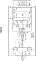
- the arc furnace facility comprises a polyphase power supply system 1 connected to a grid G and an arc furnace 2 connected to the power supply system 1.
- the power supply system 1 supplies the arc furnace 2 form electrical energy supplied by the grid G.
- Each of the power supply system 1 and the polyphase arc furnace 2 may have two phases or more than three phases, the grid G having the same number of phases than the power supply system 1.
- the arc furnace 2 comprises a set of electrodes comprising three electrodes 2a, 2b, 2c.
- the electrodes 2a, 2b, 2c supplied by the power supply system 1 generate electric arcs between the electrodes 2a, 2b, 2c to melt the contents of the arc furnace 2, for example scrap.
- the power supply system 1 comprises three inputs 3, 4, 5, each input being connected to a different phase of the grid G, and three outputs 6, 7, 8.
- Each output 6, 7, 8 is connected to an electrode 2a, 2b, 2c.
- the power supply system 1 further comprises a power converter 9, a transformer 10, a control circuit 11, current sensors, and voltage sensors.
- the control circuit 11 may comprise a processing unit.
- the power supply system 1 comprises first disconnecting means comprising a first disconnector 13 and a third disconnector 15, and second disconnecting means comprising a second disconnector 14.
- the first disconnecting means and the second disconnecting means are controlled by the control circuit 11.
- the power converter 9 comprises three inputs 16, 17, 18 and three outputs 19, 20, 21.
- Each input 16, 17, 18 of the power converter 9 is connected to a different input 3, 4, 5 of the power supply system 1.
- the transformer 10 further comprises a primary circuit including three phases 22, 23, 24 and a secondary circuit including three phases 25, 26, 27.
- Each phase 25, 26, 27 of the secondary circuit is connected to a different output 6, 7, 8 of the power supply system 1.
- Each phase 25, 26, 27 of the secondary circuit comprises a sensing module 300, 301, 302 comprising a voltage sensor and a current sensor measuring a voltage and a current of the said phase.
- the first disconnector 13 connects each input 16, 17, 18 of the power converter 9 to a different phase 22, 23, 24 of the primary circuit
- the second disconnector 14 connects each output 19, 20, 21 of the power converter 9 to a different phase 22, 23, 24 of the primary circuit.
- the third disconnector 15 connects each input 16, 17, 18 of the power converter 9 to a different output 19, 20, 21 of the power converter 9.
- the first disconnecting means do not comprise the third disconnector 15, the inputs 16, 17, 18 of the power converter 9 being not connected to the outputs 19, 20, 21 of the power converter 9.
- Figure 2 illustrates an example of the power converter 9.
- the power converter 9 further comprises an input device 28, a link circuit 29 comprising a first bus 30 and a second bus 31, and an output device 32.
- Each input 16, 17, 18 of the power converter 9 comprises a sensing module 303, 304, 305 comprising a voltage sensor and a current sensor measuring a voltage and a current of the said input.
- Each output 19, 20, 21 of the power converter 9 comprises a sensing module 306, 307, 308 comprising a voltage sensor and a current sensor measuring a voltage and a current of the said input.
- the first bus 30 may have a potential higher than the second bus 31.
- V DC The voltage between the first and second buses 30, 31 is noted V DC .
- the link circuit 25 may further comprise a filtering module 33 including two energy storage devices 33a, 33b connected in series.
- a first end of a first energy storage device 33a is connected to the first bus 30, a first end of the second energy storage 33b is connected to the second bus 31, and the first end of the second energy storage 33b and the second end of the first energy storage 33a are connected to a connecting node 33c.
- Each energy storage device 33a, 33b comprises for example a capacitor.
- the input device 28 comprises three inputs 34, 35, 36 and three outputs 37, 38, 39.
- Each input 34, 35, 36 of the input device 28 is connected to a different input 16, 17, 18 of the power converter 9.
- a first output 37 of the input device 28 is connected to the first bus 30, a second output 38 of the input device 28 is connected to the second bus 31, and the third output 39 is connected to the connecting node 33c.
- the input device 28 further comprises identical input modules 40, 41, 42.
- Each input module 40, 41, 42 is connected to a different input 34, 35, 36 of the input device 28.
- Each input module 40, 41, 42 comprises an input 40a, 41a, 42a connected to the input 34, 35, 36 of the input device 28, a first output 40b, 41b, 42b connected to the first output 37 of the input device 28, a second output 40c, 41c, 42c connected to the second output 38 of the input device 28, and a third output 40d, 41d, 42d connected to the third output 39 of the input device 28.
- the output device 32 comprises two inputs 43, 44 and three outputs 45, 46, 47.
- a first input 43 of the output device 32 is connected to the first bus 30 and the second input 44 is connected to the second bus 31.
- a first output 45 of the output device 32 is connected to a first output 19 of the power converter 9, a second output 46 is connected to a second output 20 of the power converter 9, and a third output 47 is connected to the third output 21 of the power converter 9.
- the output device 32 further comprises identical output modules 48, 49, 50.
- Each output module 48, 49, 50 comprises a first input 48a, 49a, 50a connected to the first input 43 of the output device 32, a second input 48b, 49b, 50b connected with the second input of the other output modules, and a third input 48c, 49c, 50c connected to the second input 44 of the output device 32.
- Each output module 48, 49, 50 further comprises an output 48d, 49d, 50d connected to a different output 45, 46, 47 of the output device 32.
- the input device 28 is intended to supply the link circuit 29 with a continuous voltage from the grid G.
- the output device 32 is intended to supply with electrical energy the electrodes 2a, 2b, 2c through the transformer 10.
- the energy storage devices 33a, 33b are designed to filter the continuous voltage of the link circuit 29 to stabilize the continuous voltage and to filter the current variation on the buses 30, 31.
- the filtering module 33 may decouple the input device 28 and the output device 32 to avoid that electrical perturbations generated by the arc furnace 2 are rejected on the grid G.
- the link circuit 29 may not comprise the fileting module 33, the third output 39 of the input device 28 being not connected.
- figure 3 illustrates schematically a first example of the input module 40.
- the input module 40 comprises a leg 51 comprising a first string 52 and a second string 53.
- the first string 52 comprises a first branch 54 and a second branch 55.
- Each branch 54, 55 comprises a first end 56, 57, a second end 58, 59, two switches 60, 61, 62, 63 connected in series and extending between the first and second ends 56, 57, 58, 59.
- the first branch 54 further comprises a first connecting node 64 situated between the switches 60, 61 and the second branch 55 further comprises a second connecting node 65 situated between the switches 62, 63.
- Each branch 54, 55 may comprise more than two switches, the two branches comprising a same number of switches.
- Each switch 60, 61, 62, 63 comprises a first end 60a, 61a, 62a, 63a and a second end 60b, 61b, 62b, 63b.
- the switches 60, 61 of the first branch 54 are connected in series so that the first end 61a of the switch 61 is connected to the second end 60b of the switch 60.
- the first end 56 of the first branch 54 is connected to the first remaining end 60a of the switch 60 and the second end 58 of the first branch 54 is connected to the second remaining end 61b of the switch 61.
- the remaining end of a switch is the end of the said switch which is not connected to an end of another switch.
- the switches 62, 63 of the second branch 55 are connected in series so that the first end 63a of the switch 63 is connected to the second end 62b of the switch 62.
- the first end 57 of the second branch 55 is connected to the first remaining end 62a of the switch 62 and the second end 59 of the second branch 55 is connected to the second remaining end 63b of the switch 63.
- the first end 56 of the first branch 54 is connected to the first output 40b
- the second end 59 of the second branch 55 is connected to the second output 40c
- the second end 58 of the first branch 54 and the first end 57 of the second branch 55 are connected to a third connecting node 66.
- the third connecting node 66 is connected to the third output 40d.
- the second string 53 comprises a first portion 68, and a second portion 69.
- the second string 53 may further comprise a first inductor 71.
- Each portion 68, 69 comprises a first end 73, 74, a second end 75, 76, and a plurality of switching units 77, each switching unit 77 comprising a first connection 74 and a second connection 75.
- Each portion 64, 65 comprises a same number of switching units 77.
- Each switching unit 77 includes a plurality of controllable switches and at least one energy storage device, the controllable switches being intended to bridge the energy storage device or to connect the energy storage device in each switching unit 77.
- the switching units 77 of each portion 68, 69 are connected in series so that the first connection 78 of a switching unit 77 is connected to a second connection 79 of an adjacent switching unit 77.
- the first remaining connection 78 of the switching unit 77 of the first portion 68 is connected to the first end 73 and the second remaining connection 79 of the switching unit 77 of the first portion 68 is connected to the second end 75.
- connection of a switching unit is the connection of the said switching unit which is not connected to a connection of another switching unit.
- the first end 73 of the first portion 68 is connected to the first connecting node 64 and the second end 75 is connected to a first end of the first inductor 71.
- the first remaining connection 78 of the switching unit 77 of the second portion 69 is connected to the first end 74 and the second remaining connection 79 of the switching unit 77 of the second portion 69 is connected to the second end 76.
- the first end 74 of the second portion 69 is connected to a second end of the first inductor 71 and the second end 76 is connected to the second connecting node 65.
- the second string 53 further comprises a first mid-connecting node 70 connecting the input 40a of the input module 40 to a mid-connecting node of the first inductor 71.
- the first inductor 71 permits to limit current peaks in the second string 53 and the phases of the grid G during commutations of the switching units 77.
- the second string 53 does not comprise the first inductor 71, the ends 74, 75 of the first and second portions 68, 69 and the input 40a of the input module 40 being connected to the first mid-connecting node 70, the first portion 68 or the second portion 69 comprising an inductor to limit the current peaks in the second string 53 and the second string 53 comprises another inductor connecting the input 40a of the input module 40 to the first mid-connecting node 70 to limit the current peaks in the phase of the grid G.
- the second string 53 does not comprise the first inductor 70, the ends 74, 75 of the first and second portions 68, 69 and the input 40a of the input module 40 are connected to the first mid-connecting node 70, each of the first portion 68 and the second portion 69 comprising an inductor to limit the current peaks in the second string 53 and the second string 53 may comprise another inductor connecting the input 40a of the input module 40 to the first mid-connecting node 70 to limit the current peaks in the phase of the grid G.
- Figure 4 illustrates schematically a second example of the input module 40.
- the output module 40 comprises a first portion 82 and a second portion 83.
- the input module 40 may comprise a second inductor 88.
- Each portion 82, 83 comprises a first end 84, 85, a second end 86, 87, and a plurality of switching units 77.
- the first end 84 of the first portion 82 is connected to the first output 40b of the input module 40 and the second end 87 of the second portion 83 is connected to the second output 40c of the input module 40.
- the third output 40d of the input module 40 is not connected.
- the switching units 77 of each portion 82, 83 are connected in series so that the first connection 78 of a switching unit 77 is connected to a second connection 79 of an adjacent switching unit 77.
- the first remaining connection 78 of the switching units 77 of the first portion 82 is connected to the first end 84 and the second remaining connection 79 of the switching units 77 of the first portion 82 connected to the second end 86.
- connection of a second switch unit is the connection of the said second unit which is not connected to a connection of another second switch unit.
- the first remaining connection 78 of the switching units 77 of the second portion 83 is connected to the first end 85 and the second remaining connection 79 of the switching units 77 of the second portion 83 is connected to the second end 87.
- a first end of the second inductor 88 is connected to the second end 86 of the first portion 82 and a second end of the second inductor 88 is connected to the first end 85 of the second portion 83.
- the input module 40 further comprises a second mid-connecting node 81 connecting the input 40a of the input module 40 to a mid-connecting node of the second inductor 88.
- the second inductor 88 permits to limit current peaks in the first portion 82, the second portion 83, the phases of the grid G during commutations of the switching units 77 during commutations of the second switching units 77.
- the input module 40 does not comprise the second inductor 88, the ends 85, 86 of the first portion 82 and the second portion 83 and the input 40a of the input module 40 being connected to the second mid-connecting node 81, the first portion 82 or the second portion 83 comprising an inductor to limit the current peaks in the input module 40, and the input module 40 comprises another inductor connecting the input 40a of the input module 40 to the second mid-connecting node 81 to limit the current peaks in the grid G.
- the input module 40 does not comprise the second inductor 88, the ends 85, 86 of the first portion 82 and the second portion 83 and the input 40a of the input module 40 being connected to the second mid-connecting node 81, each of the first portion 82 and the second portion 83 comprising an inductor to limit the current peaks in the input module 40, and the input module 40 may comprise another inductor connecting the input 40a of the input module 40 to the second mid-connecting node 81 to limit the current peaks in the grid G.
- figure 5 illustrates schematically a first example of the output module 48.
- the output module 44 comprises a second leg 91 comprising a fourth string 92 and a fifth string 93.
- the fourth string 92 comprises a first branch 94 and a second branch 95.
- Each branch 94, 95 comprises a first end 96, 97, a second end 98, 99, two second switches 100, 101, 102, 103 connected in series and extending between the first and second ends 96, 97, 98, 99.
- Each branch 94, 95 may comprise more than two second switches, the two branches comprising a same number of second switches.
- Each second switch 100, 101, 102, 103 comprises a first end 100a, 101a, 102a, 103a and a second end 100b, 101b, 102b, 103b.
- the second switches 100, 101 of the first branch 94 are connected in series so that the first end 101a of the second switch 101 is connected to the second end 100b of the second switch 100.
- the first end 96 of the first branch 94 is connected to the first remaining end 100a of the second switch 100 and the second end 98 of the first branch 94 is connected to the second remaining end 101b of the second switch 101.
- the remaining end of a second switch is the end of the said second switch which is not connected to an end of another second switch.
- the second switches 102, 103 of the second branch 95 are connected in series so that the first end 103a of the second switch 103 is connected to the second end 102b of the second switch 102.
- the first end 97 of the second branch 95 is connected to the first remaining end 102a of the second switch 102 and the second end 99 of the second branch 95 is connected to the second remaining end 103b of the second switch 103.
- the first branch 94 further comprises a fourth connecting node 104 situated between the second switches 100, 101 and the second branch 95 further comprises a fifth connecting node 105 situated between the second switches 102, 103.
- the first end 96 of the first branch 94 is connected to the first input 48a
- the second end 99 of the second branch 95 is connected to the second input 48b
- the second end 98 of the first branch 94 and the first end 97 of the second branch 95 are connected to a sixth connecting node 1000.
- the sixth connecting node 1000 is connected to the third input 48c.
- Each branch 104, 105 comprises the same number of second switches.
- the fifth string 93 comprises a third portion 107 and a fourth portion 108.
- the fifth string 93 may further comprise a third inductor 109.
- Each portion 107, 108 comprises a first end 112, 113 a second end 114, 115, and a plurality of second switching units 116, each second switching unit 116 comprising a first connection 117 and a second connection 118.
- Each portion 107, 108 comprises a same number of second switching units 116.
- the second switching units 116 of each portion 107, 108 are connected in series so that the first connection 117 of a second switching unit 116 is connected to a second connection 118 of an adjacent switching unit 116.
- the first remaining connection 117 of the second switching units 116 of the third portion 107 is connected to the first end 112 and the second remaining connection 118 of the second switching units 116 of the third portion 107 is connected to the second end 114.
- connection of a second switch is the end of the said second switch which is not connected to an end of another second switch.
- the first end 112 of the third portion 107 is connected to the fourth connecting node 104 and the second end 114 is connected to a first end of the third inductor 109.
- the first remaining connection 117 of the second switching units 116 of the fourth portion 108 is connected to the first end 113 and the second remaining connection 118 of the second switching units 116 of the fourth portion 108 is connected to the second end 115.
- the first end 113 of the fourth portion 108 is connected to a second end of the third inductor 109 and the second end 115 is connected to the fifth connecting node 105.
- the fifth string 93 further comprises a third mid-connecting node 106 connecting the output 48d of the output module 48 to a mid-connecting node of the third inductor 109.
- the third inductor 109 permits to limit current peaks in the fifth string 93 and the phases of the arc furnace 2 during commutations of the switching units 116.
- the fifth string 93 does not comprise the third inductor 109, the ends 113, 114 of the third and fourth portions 107, 108 and the output 48d of the output module 48 being connected to the third mid-connecting node 106, the third portion 107 or the fourth portion 108 comprising an inductor to limit the current peaks in the fifth string 93, and the fifth string 93 comprises another inductor connecting the output 40d of the output module 40 to the third mid-connecting node 106 to limit the current peaks in the phase of the arc furnace 2.
- the fifth string 93 does not comprise the third inductor 109, the ends 113, 114 of the third and fourth portions 107, 108 and the output 40d of the output module 40 being connected to the third mid-connecting node 106, each of the third portion 107 and the fourth portion 108 comprising an inductor to limit the current peaks in the fourth string 108, and the fourth string 108 may comprise another inductor connecting the output 40d of the output module 40 to the third mid-connecting node 106 to limit the current peaks in the phase of the arc furnace 2.
- Figure 6 illustrates schematically a second example of the output module 48.
- the output module 48 comprises a first portion 121 and a second portion 122.
- the output module 48 may comprise a fourth inductor 127.
- Each portion 121, 122 comprises a first end 123, 124, a second end 125, 126, and a plurality of second switching units 116.
- the first end 123 of the first portion 121 is connected to the first input 48a of the output module 48 and the second end 126 of the second portion 122 is connected to the second input 48b of the output module 48.
- the third input 48c of the output module 48 is not connected.
- the second switching units 116 of each portion 121, 122 are connected in series so that the first connection 117 of a switching unit 116 is connected to a second connection 118 of an adjacent switching unit 116.
- the first remaining connection 117 of the second switching units 116 of the first portion 121 is connected to the first end 123 and the second remaining connection 118 of the second switching units 116 of the first portion 121 connected to the second end 125.
- connection of a second switch unit is the connection of the said second unit which is not connected to a connection of another second switch unit.
- the first remaining connection 117 of the second switching units 116 of the second portion 122 is connected to the first end 124 and the second remaining connection 118 of the second switching units 116 of the second portion 122 is connected to the second end 126.
- a first end of the fourth inductor 127 is connected to the second end 86 of the first portion 121 and a second end of the fourth inductor 127 is connected to the first end 124 of the second portion 122.
- the output module 48 further comprises a fourth mid-connecting node 120 connecting the output 48da of the output module 48 to a mid-connecting node of the fourth inductor 127.
- the fourth inductor 127 permits to limit current peaks in the first portion 121, the second portion 122, the phases of the arc furnace 2 during commutations of the switching units 116.
- the output module 48 does not comprise the fourth inductor 127, the ends 124, 125 of the first portion 121 and the second portion 122 and the output 48d of the output module 48 being connected to the fourth mid-connecting node 120, the first portion 121 or the second portion 122 comprising an inductor to limit the current peaks in the output module 48, and the output module 48 comprises another inductor connecting the output 48d of the output module 48 to the fourth mid-connecting node 120 to limit the current peaks in the phases of the arc furnace 2.
- the output module 48 does not comprise the fourth inductor 127, the ends 124, 125 of the first portion 121 and the second portion 122 and the output 48d of the output module 48 being connected to the fourth mid-connecting node 120, each of the first portion 121 and the second portion 122 comprising an inductor to limit the current peaks in the output module 48, and the output module 48 may comprise another inductor connecting the output 48d of the output module 48 to the fourth mid-connecting node 120 to limit the current peaks in the phases of the arc furnace 2.
- the first example of the input module 40 illustrated on figure 3 and the first example of the output module 48 illustrated on figure 5 are known from the EP 2 713 495
- the second example of the input module 40 illustrated on figure 4 and the second example of the output module 48 illustrated on figure 6 are known from the EP 2 329 684 .
- the voltage between the first and second connecting nodes 64, 65 of each input module 40, 41, 42 as illustrated on figure 3 and the voltage between the fourth and fifth connecting nodes 104, 105 of each output module 48, 49, 50 as illustrated on figure 5 is equal to V DC /2 so that the number of switching units 77 and second switching units 116 is reduced, at least divided by two, compared to the number of switching units 77 and second switching units 116 in the second example of input modules 40, 41, 42 and output modules 48, 49, 50 as illustrated on figures 4 and 6 .
- the reduction of switching units 77 and second switching units 116 reduces the complexity of the power converter 9 and the power loses generated by the power converter 9.
- Figure 7 illustrates schematically an embodiment of the switches 60, 61, 62, 63.
- the switch 60, 61, 62, 63 comprises a diode 137 extending between the first and the second ends of the switch 60, 61, 62, 63 so that the anode of the diode 137 is connected to the second end 60b, 61b, 62b, 63b of the switch and the cathode is connected to the first end 60a, 61a, 62a, 63a of the switch 60, 61, 62, 63.
- the first example of the switch comprising the diode 137 simplify the implementation of the switches 60, 61, 62, 63 in the input modules 40, 41, 42.
- Each switch 60, 61, 62, 63 may comprise a plurality of diodes 137 in series so that the anode of one diode is connected to the cathode of another diode.
- the diode 137 is designed to support a voltage at least equal to V DC /2.
- Each switch 60, 61, 62, 63 implemented in the first example of the input modules 40, 41, 42 or in the first example of the output modules 48, 49, 50 may comprise a plurality of diodes 137 in series so that the anode of one diode is connected to the cathode of another diode, the number of diodes 137 being determined so that the set of diodes 137 in series supports a voltage at least equal to V DC /2.
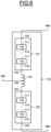
- Figure 8 illustrates schematically another embodiment of the switches 60, 61, 62, 63 and the second switches 100, 101, 102, 103.
- Each switch of the switches 60, 61, 62, 63 and the second switches 100, 101, 102, 103 comprises the diode 137 extending between the first and the second ends of the switch 60, 61, 62, 63, 100, 101, 102, 103 so that the anode of the diode 137 is connected to the second end 60b, 61b, 62b, 63b, 100b, 101b, 102b, 103b of the switch and the cathode is connected to the first end 60a, 61a, 62a, 63a, 100a, 101a, 102a, 103a of the switch 60, 61, 62, 63, 100, 101, 102, 103.
- Each switch 60, 61, 62, 63, 100, 101, 102, 103 further comprises a gate turn off thyristor 138.
- the gate of the gate turn off thyristor 138 is connected to the control circuit 11, the anode of the gate turn off thyristor 138 is connected to the cathode of the diode 137, and the cathode of the gate turn off thyristor 138 is connected to the anode of the diode 137.
- Each switch 60, 61, 62, 63 may comprise a plurality of gate of the gate turn off thyristors 138 in series so that the anode of one thyristor is connected to the cathode of another thyristor.
- the gate turn off thyristor 138 is designed to support a voltage at least equal to V DC /2.
- Each switch 60, 61, 62, 63 implemented in the first example of the input modules 40, 41, 42 or in the first example of the output modules 48, 49, 50 may comprise a plurality of gate turn off thyristors 138 in series so that the anode of one diode is connected to the cathode of another diode, the number of gate turn off thyristors 138 being determined so that the set of gate turn off thyristors 138 in series supports a voltage at least equal to V DC /2.
- Figure 9 illustrates schematically yet another embodiment of the switches 60, 61, 62, 63 and the second switches 100, 101, 102, 103.
- Each switch of the switches 60, 61, 62, 63 and the second switches 100, 101, 102, 103 comprises the diode 137 extending between the first and the second ends of the switch 60, 61, 62, 63, 100, 101, 102, 103 so that the anode of the diode 137 is connected to the second end 60b, 61b, 62b, 63b, 100b, 101b, 102b, 103b of the switch and the cathode is connected to the first end 60a, 61a, 62a, 63a, 100a, 101a, 102a, 103a of the switch 60, 61, 62, 63, 100, 101, 102, 103.
- Each switch 60, 61, 62, 63, 100, 101, 102, 103 further comprises a field effect transistor 139.
- the field effect transistor 139 may be an insulated gate bipolar transistor IGBT.
- the gate of the transistor 139 is connected to the control circuit 11, the drain of the transistor 139 is connected to the cathode of the diode 137 and the source of the transistor 139 is connected to the anode of the diode 137.
- Each switch 60, 61, 62, 63 may comprise a plurality of transistors 139 in series so that the drain of one transistor is connected to the source of another transistor.
- the transistor 139 is designed to support a voltage at least equal to V DC /2.
- Each switch 60, 61, 62, 63 implemented in the first example of the input modules 40, 41, 42 or in the first example of the output modules 48, 49, 50 may comprise a plurality of transistors 139 in series so that the drain of one transistor is connected to the source of another transistor, the number of transistors 139 being determined so that the set of transistors 139 in series supports a voltage at least equal to V DC /2.
- the inputs modules 40, 41, 42 may comprise one embodiment of the switches 60, 61, 62, 63 illustrated on figures 7, 8, 9
- the output modules 48, 49, 50 may comprise one embodiment of the second switches 100, 101, 102, 103 illustrated on figure 8, 9
- the embodiment of the switches 60, 61, 62, 63 and the embodiment of the second switches 100, 101, 102, 103 may be different so that for example the switches 60, 61, 62, 63 comprise the embodiment illustrated on figure 8 and the second switches 100, 101, 102, 103 comprise the embodiment illustrated on figure 9 .
- the embodiment of the switches 60, 61, 62, 63 and the embodiment of the second switches 100, 101, 102, 103 may have the same architecture, for example the switches 60, 61, 62, 63 and the second switches 100, 101, 102, 103 comprise the embodiment illustrated on figure 11 .
- Figure 10 illustrates schematically a first embodiment of the switching unit 77 and the second switching unit 116.
- Each one of the switching unit 77 and the second switching unit 116 comprises two controllable switches 140, 141 and a second energy storage 142 comprising a first end 142a and a second end 142b.
- the second energy storage 142 comprises for example a capacitor.
- Each controllable switch 140, 141 comprises a first end 140a, 141a, a second end 140b, 141b, and a control input 140c, 141c connected to the control circuit 11.
- the first end 140a of a first controllable switch 140 is connected to the first end 142a of the second energy storage 142.
- the second end 140b of the first controllable switch 140 and the first end 141a of the second controllable switch 141 are connected to the first end 78, 117 of the switching unit 77 or second switching unit 116.
- the second end 141b of the second controllable switch 141 is connected to the second end 142b of the second energy storage 142 and to the second end 79, 118 of the switching unit 77 or second switching unit 116.
- controllable switches 140, 141 are identical, only the first switch 130 is detailed.
- the first switch 140 comprises a second transistor 143 and a second diode 144.
- the second transistor 143 may be a field effect transistor, for example an IGBT transistor.
- the gate of the second transistor 143 is connected to the control input 140c, the drain of the second transistor 143 and the cathode of the second diode 144 are connected to the first end 140a, and the source of the second transistor 143 and the anode of the second diode 144 are connected to the second end 140b.
- Figure 11 illustrates schematically a second embodiment of the switching unit 77 and the second switching unit 116.
- Each one of the switching units 77 and the second switching units 126 comprises four controllable switches 145, 146, 147, 148 identical to the controllable switches 140, 141 of the first embodiment illustrated on figure 13 .
- Each controllable switches 145, 146, 147, 148 comprises a first end 145a, 146a, 147a, 148a, a second end 145b, 146b, 147b, 148b, and a control input 145b, 146b, 147b, 148b connected to the control circuit 11
- Each controllable switches 145, 146, 147, 148 further comprises the second energy storage 142.
- the first end 145a of a first controllable switch 145 and the first end 146a of a second controllable switch 146 are connected to the first end 142a of the second energy storage 142.
- the second end 147b of a third controllable switch 147 and the second end 148b of the fourth controllable switch 148 are connected to the second end 142b of the second energy storage 142.
- the second end 145b of the first controllable switch 145 and the first end 147a of the third controllable switch 147 are connected to the first end 78, 117 of the switching unit 77 or second switching unit 116.
- the second end 146b of the second controllable switch 146 and the first end 148a of the fourth controllable switch 148 are connected to the second end 79, 118 of the switching unit 77 or second switching unit 116.
- the switching units 77 and the second switching units 116 according to the first embodiment illustrated on figure 13 have two states, each state delivering a different voltage value on the ends of the switching units 77 and the second switching units 116.
- the switching units 77, 116 deliver a positive compensating voltage Vcc, and in a second state a nil voltage.
- the switching units 77 and the second switching units 116 according to the second embodiment illustrated on figure 14 have three states, each state delivering a different voltage value on the ends of the switching units 77 and the second switching units 116.
- the switching units 77, 116 deliver a positive voltage Vcc, in a second state a nil voltage, and in a third state a negative compensating voltage -Vcc.
- the embodiment of the switching units 77 of inputs modules 40, 41, 42 and the embodiment of the second switching units 116 of the output modules 48, 49, 50 may be identical or different, for example the switching units 77 may have the architecture of the first embodiment illustrated on figure 13 and the second switching units 116 may have the architecture of the second embodiment illustrated on figure 14.
- Figure 12 illustrates schematically a third example of the input modules 40, 41, 42.
- the first module 40 is detailed in the following.
- the second example differs from the first example of the input module 40 illustrated on figure 3 in that the leg 51 further comprises two compensating modules 149, 150 comprising a first end 151, 152, a second end 153, 154, and a plurality of switching units 77.
- the first end 151 of a first compensating module 149 is connected with the first end of the first compensating module of the other inputs modules 41, 42 and the second end 153 of the second compensating module 150 is connected with the second end of the second compensating module of the other inputs modules 41, 42.
- the second end 153 of the first compensating module 149 is connected to the first connecting node 64 and the first end 136 of the second compensating module 134 is connected to the second connecting node 65.
- Each compensating module 149, 150 comprises a same number of switching units 77 connected in series so that the first end 78 of a switching unit 77 is connected to the second end 79 of an adjacent switching unit 77.
- the first remaining connection 78 of the switching units 77 of the first compensating module 149 is connected to the first end 151 of the first compensating module 149 and the second remaining connection 79 of the switching units 77 of the first compensating module 149 is connected to the second end 153 of the first compensating module 149.
- the first remaining connection 78 of the switching units 77 of the second compensating module 150 is connected to the first end 152 of the second compensating module 150 and the second remaining connection 79 of the switching units 77 of the second compensating module 150 is connected to the second end 154 of the second compensating module 150.
- the two compensating modules 149, 150 act as static synchronous compensator STATCOM to enhance the quality of filtering of the supply system 1 to limit the rejections of the arc furnace on the grid G.
- control unit 11 cannot control the commutation of the switches to limit the rejections on the grid G, only the output modules contribute to reduce the rejections in the grid G.
- Figure 13 illustrates a second example of the arc furnace facility.
- the arc furnace facility differs from the arc furnace facility illustrated on figure 1 in that the arc furnace facility comprises a direct voltage arc furnace 155.
- the direct voltage arc furnace 155 comprises the set of electrodes comprising only one electrode 155a.
- the power supply system 1 further comprises a rectifier 156.
- the rectifier 156 comprises a plurality of inputs 157, 158, 159, each input 157, 158, 159 being connected to a different phase 25, 26, 27 of the secondary circuit of the transformer 10.
- the rectifier 156 further comprises a first output 160 connected to an enclosure 155b of the arc furnace 155 and a second output 161 connected to the electrode 155a of the arc furnace 155.
- the rectifier 156 comprises the same number of identical legs 162, 163, 164 as the number of phases of the secondary circuit of the transformer 10, each leg 162, 163, 164 being connected to a different phase.
- Each leg 162, 163, 164 comprises a first connection 162a, 163a, 164a, a second connection 162b, 163b, 164b, and a third connection 162c, 163c, 164c.
- the first connection 162a, 163a, 164a of each leg 162, 163, 164 is connected to the first output 160 of the rectifier 156
- the second connection 162b, 163b, 164b of each leg 162, 163, 164 is connected to the second output 161 of the rectifier 156
- the third connection 162c, 163c, 164c is connected to a different input 157, 158, 159 of the rectifier 156.
- legs 162, 163, 164 are identical, only a first leg 162 is detailed.
- the first leg 162 comprises two identical power diodes 165, 166 connected in series.
- the cathode of a first power diode 165 is connected to the first connection 162a, the anode of the first power diode 165 and the cathode of the second power diode 166 are connected to the third connection 162c, and the anode of the second power diode 166 is connected to the second connection 162b.
- the rectifier 156 rectifies the voltage delivered by each phase of the secondary circuit to supply the electrode 155a of the direct voltage arc furnace 155.
- the rectifier 156 may comprise an active rectifier made from controlled semiconductor, for example transistors and/or gate turn off thyristors.
- a first example of a method implementing the power supply system 1 is presented.
- first disconnecting means are open so that the first disconnector 13 and the third disconnector 15 are open and the second disconnecting means are closed so that the second disconnector 14 is closed.
- the control circuit 11 controls the input modules 40, 41, 42 and the outputs modules 48, 49, 50 to supply the set of electrodes and to stabilize the lay and the voltage delivered by the grid G to reduce reactions in the grid G generated by the arc furnace 2, 155.
- the control circuit 11 controls independently each switching unit 77 and each second switching unit 116, and if applicable each switch 60, 61, 62, 63 and each second switch 100, 101, 102, 103 to supply the set of electrodes and to stabilize the lay and the voltage delivered by the grid G to reduce reactions in the grid G.
- control circuit 11 closes the first disconnecting means so that currents flow from the grid G to the primary circuit through the first disconnector 13 and opens the second disconnecting means so that no current flows from the outputs of the power converter 9 to the primary circuit.
- the arc furnace 2, 155 is directly supplied by the grid G through the first disconnector 13.
- the control circuit 11 may further controls independently each switching unit 77 and each second switching unit 116, and if applicable each switch 60, 61, 62, 63 and each second switch 100, 101, 102, 103 to stabilize the dependency and the voltage delivered by the grid G to reduce reactions in the grid G.
- the power converter 9 acts as a static compensator STATCOM to reduce the reactions on the grid G.
- control circuit 11 closes the third disconnector 15 to inject power in the grid G.
- the first and second disconnecting means and the control circuit 11 allow to continue to implement the arc furnace 2, 155.
Landscapes
- Engineering & Computer Science (AREA)
- Power Engineering (AREA)
- Physics & Mathematics (AREA)
- Plasma & Fusion (AREA)
- Nonlinear Science (AREA)
- Ac-Ac Conversion (AREA)
- Dc-Dc Converters (AREA)
- Inverter Devices (AREA)
Abstract
- a power converter (9), and
- a polyphase transformer (10),
o to control the power converter to supply the electrode and to stabilize the courant and the voltage delivered by the grid to reduce reactions in the grid when the first disconnecting means are open and the second disconnecting means are closed, and
o to control the power converter to stabilize the courant and the voltage delivered by the grid to reduce reactions in the grid when the first disconnecting means are closed and the second disconnecting means are open.
Description
- The present invention concerns arc furnaces, and more particularly a power supply system for arc furnaces, and an arc furnace facility comprising an arc furnace and such a power supply system.
- Arc furnaces are highly nonlinear loads resulting in considerable reactions on the power supply system, in particular so-called flicker.
-
- The power supply system comprises an indirect power converter and a polyphase transformer.
- The indirect power converter supplies a primary circuit of the transformer. A secondary circuit of the transformer supplies electrodes of the arc furnace.
- The indirect power converter is controlled to minimize reactions on the grid in order to supress the flicker and in order to comply with grid quality standards.
- During the tuning of the power supply system or when the indirect power converter goes wrong, the power supply system may be stop, for example following reactions on the grid generated by the indirect power converter greater than acceptable reactions.
- During these more or less log stops, the arc furnace does not melt scraps to produce molten steel.
- Machines using molten steel, for example rolling mills, are forced to be stopped during stops of the arc furnace generated production losses.
- It is therefore proposed to remedy the disadvantages related to arc furnace power supply systems known from the prior art.
- In view of the foregoing the invention proposes a power supply system for arc furnace including:
- a power converter comprising an input intended to be connected to a polyphase supply grid and an output, and
- a polyphase transformer comprising a primary circuit and a secondary circuit intended to be connected to at least one electrode of the arc furnace.
- The power supply system further comprises first disconnecting means connecting the input of the power converter to the primary circuit, second disconnecting means connecting the output of the power converter to the primary circuit, and the power supply system further comprises a control circuit configured:
- o to control the power converter to supply the electrode and to stabilize the courant and the voltage delivered by the grid to reduce reactions in the grid when the first disconnecting means are open and the second disconnecting means are closed, and
- o to control the power converter to stabilize the courant and the voltage delivered by the grid to reduce reactions in the grid when the first disconnecting means are closed and the second disconnecting means are open.
- Preferably, the first disconnecting means further connect the input of the power converter to the output of the power converter, the control circuit being further configured to control the power converter to supply the grid with power when the first disconnecting means are closed.
- Advantageously, the control circuit is further configured to close the first disconnecting means and to open the second disconnecting means.
- Preferably, the power converter comprises an input device, a link circuit comprising a first bus and a second bus, and an output device, wherein:
- the input device comprises a plurality of input modules, each input module being connected to the first bus and the second bus and being intended to be connected to a different phase of the supply grid to supply the link circuit with a continuous voltage from the said phase of the supply grid,
- the output device comprises a plurality of output modules, each output module being connected to the first bus and second bus and to the primary circuit to supply the transformer with an alternative voltage from the circuit link,
- a leg including:
- o a first string connected to the first and second bus and comprising a plurality of switches connected in series, a first connecting node situated between two switches, a second connecting node situated between two switches and a third connecting nodes situated between two switches, and
- o a second string comprising:
- a first mid-connecting node,
- a plurality of switching units connected in series and extending between the first and second connecting points,
- the first mid-connecting node being between two switching units so that the number of switching units between the first connecting point and the first mid-connecting node is equal to the number of switching units between the second connecting point and the first mid-connecting node, the first mid-connecting node being intended to be connected to the said phase of the supply grid,
- the third connecting node of each input module being connected together,
- the control circuit being configured to control the switches, the switching units, and the output modules.
- Advantageously, the leg further comprises two compensating modules, each compensating module comprising a first end and a plurality of switching units connected in series, the switching units of the first compensating module extending between the first connecting node and the first end of the first compensating unit, the switching units of the second compensating module extending between the second connecting node and the first end of the second compensating module, the first ends of the first and second compensating units being connected together, the control circuit being further configured to control the switching units of the compensating modules.
- Preferably, the power converter comprises an input device, a link circuit comprising a first bus and a second bus, and an output device, wherein:
- the input device comprises a plurality of input modules, each input module being connected to the first bus and the second bus and being intended to be connected to a different phase of the supply grid to supply the link circuit with a continuous voltage from the said phase of the supply grid,
- the output device is connected to the first bus and second bus and to the primary circuit to supply the transformer with an alternative voltage from the circuit link,
each input module comprises a third string comprising:- a second mid-connecting node, and
- a plurality of switching units connected in series and extending between the first and second bus,
- the second mid-connecting node being between two second switching units so that the number of second switching units between the first bus and the second mid-connecting node is equal to the number of switching units between the second bus and the second mid-connecting node, the second mid-connecting node being connected to a phase of the primary circuit.
- Advantageously, each output module comprises:
- a second leg comprising:
- o a fourth string connected to the first and second bus and comprising a plurality of second switches connected in series and a fourth connecting node situated between two second switches, a fifth connecting node situated between two second switches, and a sixth connecting node situated between two second switches, and
- o a fifth string comprising:
- a third mid-connecting node,
- a plurality of second switching units connected in series and extending between the fourth and the fifth connecting nodes,
- the third mid-connecting node being between two switching units so that the number of switching units between the first connecting point and the third mid-connecting node is equal to the number of switching units between the second connecting point and the third mid-connecting node, the third mid-connecting node being connected to a phase of the primary circuit,
- the sixth connecting node of each output module being connected together,
- the control circuit being further configured to control the second switches and the second switching units.
- Preferably, each output module comprises a sixth string comprising:
- a fourth mid-connecting node, and
- a plurality of second switching units connected in series and extending between the first and second bus,
- the fourth mid-connecting node being between two second switching units so that the number of second switching units between the first bus and the fourth mid-connecting node is equal to the number of switching units between the second bus and the fourth mid-connecting node, the fourth mid-connecting node being connected to a phase of the primary circuit.
- Another object of the invention relates to an arc furnace facility.
- The arc furnace facility comprises an arc furnace including at least one electrode and a power supply system as defined above, wherein the electrode is connected to at least one phase of the secondary circuit of the polyphase transformer.
- Advantageously, the arc furnace comprises a plurality of electrodes, each electrode being connected to a different phase of the secondary circuit.
- Preferably, the power supply system further comprises a rectifier connected to the electrode and to each phase of the secondary circuit to supply the electrode with a continuous voltage from the secondary circuit.
- Another object of the invention relates to a method for controlling a power supply system of an arc furnace, the power supply system including:
- a power converter comprising an input connected to a polyphase supply grid and an output, and
- a polyphase transformer comprising a primary circuit and a secondary circuit connected to at least one electrode of the arc furnace.
- The method comprises:
- o controlling the power converter to supply the electrode and to stabilize the courant and the voltage delivered by the grid to reduce reactions in the grid when first disconnecting means are open and second disconnecting means are closed, and
- o controlling the power converter to stabilize the courant and the voltage delivered by the grid to reduce reactions in the grid when the first disconnecting means are closed and the second disconnecting means are open,
- the first disconnecting means connecting the input of the power converter to the primary circuit and the second disconnecting means connecting the output of the power converter to the primary circuit.
- Preferably, the first disconnecting means further connect the input of the power converter to the output of the power converter, the method further comprising controlling the power converter to supply the grid with power when the first disconnecting means are closed.
- Other characteristics and advantages of the invention will emerge on reading the following description of embodiments of the invention, provided solely by way of non-limiting examples and with reference to the drawings in which:
-
Figure 1 illustrates schematically a first example of an arc furnace facility according to the invention, -
Figure 2 illustrates schematically an example of a power converter according to the invention, -
Figure 3 illustrates schematically a first example of an input module according to the invention, -
Figure 4 illustrates schematically a second example of the input module known form the prior art, -
Figure 5 illustrates schematically a first example of an output module according to the invention, -
Figure 6 illustrates schematically a second example of the output module know form the prior art, -
Figure 7 illustrates schematically an embodiment of switches according to the invention, -
Figure 8 illustrates schematically another embodiment of the switches according to the invention, -
Figure 9 illustrates schematically another embodiment of the switches according to the invention, -
Figure 10 illustrates schematically a first embodiment of switching units according to the invention, -
Figure 11 illustrates schematically a second embodiment of switching units according to the invention, -
Figure 12 illustrates schematically a third example of the input module according to the invention, and -
Figure 13 illustrates a second example of the arc furnace facility according to the invention. -
Figure 1 illustrates a first example of an arc furnace facility. - The arc furnace facility comprises a polyphase power supply system 1 connected to a grid G and an
arc furnace 2 connected to the power supply system 1. - The power supply system 1 supplies the
arc furnace 2 form electrical energy supplied by the grid G. - It is assumed that the power supply system 1 and the
polyphase arc furnace 2 have each three phases, the grid G been a three phases supply grid. - Each of the power supply system 1 and the
polyphase arc furnace 2 may have two phases or more than three phases, the grid G having the same number of phases than the power supply system 1. - The
arc furnace 2 comprises a set of electrodes comprising threeelectrodes - The
electrodes electrodes arc furnace 2, for example scrap. - The power supply system 1 comprises three
inputs 3, 4, 5, each input being connected to a different phase of the grid G, and threeoutputs - Each
output electrode - The power supply system 1 further comprises a
power converter 9, atransformer 10, acontrol circuit 11, current sensors, and voltage sensors. - The
control circuit 11 may comprise a processing unit. - The power supply system 1 comprises first disconnecting means comprising a
first disconnector 13 and athird disconnector 15, and second disconnecting means comprising asecond disconnector 14. - The first disconnecting means and the second disconnecting means are controlled by the
control circuit 11. - The
power converter 9 comprises threeinputs outputs - Each
input power converter 9 is connected to adifferent input 3, 4, 5 of the power supply system 1. - The
transformer 10 further comprises a primary circuit including three phases 22, 23, 24 and a secondary circuit including threephases - Each
phase different output - Each
phase sensing module - The
first disconnector 13 connects eachinput power converter 9 to a different phase 22, 23, 24 of the primary circuit, and thesecond disconnector 14 connects eachoutput power converter 9 to a different phase 22, 23, 24 of the primary circuit. - The
third disconnector 15 connects eachinput power converter 9 to adifferent output power converter 9. - In variant, the first disconnecting means do not comprise the
third disconnector 15, theinputs power converter 9 being not connected to theoutputs power converter 9. -
Figure 2 illustrates an example of thepower converter 9. - The
power converter 9 further comprises aninput device 28, alink circuit 29 comprising afirst bus 30 and asecond bus 31, and anoutput device 32. - Each
input power converter 9 comprises asensing module - Each
output power converter 9 comprises asensing module - The
first bus 30 may have a potential higher than thesecond bus 31. - The voltage between the first and
second buses - The
link circuit 25 may further comprise a filtering module 33 including twoenergy storage devices - A first end of a first
energy storage device 33a is connected to thefirst bus 30, a first end of thesecond energy storage 33b is connected to thesecond bus 31, and the first end of thesecond energy storage 33b and the second end of thefirst energy storage 33a are connected to a connectingnode 33c. - Each
energy storage device - The
input device 28 comprises threeinputs outputs - Each
input input device 28 is connected to adifferent input power converter 9. - A
first output 37 of theinput device 28 is connected to thefirst bus 30, asecond output 38 of theinput device 28 is connected to thesecond bus 31, and thethird output 39 is connected to the connectingnode 33c. - The
input device 28 further comprisesidentical input modules - Each
input module different input input device 28. - Each
input module input input input device 28, afirst output first output 37 of theinput device 28, asecond output second output 38 of theinput device 28, and athird output third output 39 of theinput device 28. - The
output device 32 comprises twoinputs outputs - A
first input 43 of theoutput device 32 is connected to thefirst bus 30 and thesecond input 44 is connected to thesecond bus 31. - A
first output 45 of theoutput device 32 is connected to afirst output 19 of thepower converter 9, asecond output 46 is connected to asecond output 20 of thepower converter 9, and athird output 47 is connected to thethird output 21 of thepower converter 9. - The
output device 32 further comprisesidentical output modules - Each
output module first input first input 43 of theoutput device 32, asecond input third input second input 44 of theoutput device 32. - Each
output module output different output output device 32. - The
input device 28 is intended to supply thelink circuit 29 with a continuous voltage from the grid G. - The
output device 32 is intended to supply with electrical energy theelectrodes transformer 10. - The
energy storage devices link circuit 29 to stabilize the continuous voltage and to filter the current variation on thebuses - The filtering module 33 may decouple the
input device 28 and theoutput device 32 to avoid that electrical perturbations generated by thearc furnace 2 are rejected on the grid G. - In variant, the
link circuit 29 may not comprise the fileting module 33, thethird output 39 of theinput device 28 being not connected. - As the
input modules figure 3 illustrates schematically a first example of theinput module 40. - The
input module 40 comprises aleg 51 comprising afirst string 52 and asecond string 53. - The
first string 52 comprises afirst branch 54 and asecond branch 55. - Each
branch first end second end switches - The
first branch 54 further comprises a first connectingnode 64 situated between theswitches 60, 61 and thesecond branch 55 further comprises a second connectingnode 65 situated between theswitches 62, 63. - Each
branch - Each
switch first end second end - The
switches 60, 61 of thefirst branch 54 are connected in series so that thefirst end 61a of theswitch 61 is connected to thesecond end 60b of the switch 60. - The
first end 56 of thefirst branch 54 is connected to the first remainingend 60a of the switch 60 and thesecond end 58 of thefirst branch 54 is connected to the second remainingend 61b of theswitch 61. - The remaining end of a switch is the end of the said switch which is not connected to an end of another switch.
- The
switches 62, 63 of thesecond branch 55 are connected in series so that thefirst end 63a of theswitch 63 is connected to thesecond end 62b of the switch 62. - The
first end 57 of thesecond branch 55 is connected to the first remainingend 62a of the switch 62 and thesecond end 59 of thesecond branch 55 is connected to the second remainingend 63b of theswitch 63. - The
first end 56 of thefirst branch 54 is connected to thefirst output 40b, thesecond end 59 of thesecond branch 55 is connected to thesecond output 40c, and thesecond end 58 of thefirst branch 54 and thefirst end 57 of thesecond branch 55 are connected to a third connectingnode 66. - The third connecting
node 66 is connected to thethird output 40d. - The
second string 53 comprises afirst portion 68, and asecond portion 69. - The
second string 53 may further comprise afirst inductor 71. - Each
portion first end second end units 77, each switchingunit 77 comprising afirst connection 74 and asecond connection 75. - Each
portion units 77. - Each switching
unit 77 includes a plurality of controllable switches and at least one energy storage device, the controllable switches being intended to bridge the energy storage device or to connect the energy storage device in each switchingunit 77. - The switching
units 77 of eachportion first connection 78 of aswitching unit 77 is connected to asecond connection 79 of anadjacent switching unit 77. - The first remaining
connection 78 of the switchingunit 77 of thefirst portion 68 is connected to thefirst end 73 and the second remainingconnection 79 of the switchingunit 77 of thefirst portion 68 is connected to thesecond end 75. - The remaining connection of a switching unit is the connection of the said switching unit which is not connected to a connection of another switching unit.
- The
first end 73 of thefirst portion 68 is connected to the first connectingnode 64 and thesecond end 75 is connected to a first end of thefirst inductor 71. - The first remaining
connection 78 of the switchingunit 77 of thesecond portion 69 is connected to thefirst end 74 and the second remainingconnection 79 of the switchingunit 77 of thesecond portion 69 is connected to thesecond end 76. - The
first end 74 of thesecond portion 69 is connected to a second end of thefirst inductor 71 and thesecond end 76 is connected to the second connectingnode 65. - The
second string 53 further comprises a firstmid-connecting node 70 connecting theinput 40a of theinput module 40 to a mid-connecting node of thefirst inductor 71. - The
first inductor 71 permits to limit current peaks in thesecond string 53 and the phases of the grid G during commutations of the switchingunits 77. - In variant, the
second string 53 does not comprise thefirst inductor 71, the ends 74, 75 of the first andsecond portions input 40a of theinput module 40 being connected to the firstmid-connecting node 70, thefirst portion 68 or thesecond portion 69 comprising an inductor to limit the current peaks in thesecond string 53 and thesecond string 53 comprises another inductor connecting theinput 40a of theinput module 40 to the firstmid-connecting node 70 to limit the current peaks in the phase of the grid G. - In another variant, the
second string 53 does not comprise thefirst inductor 70, the ends 74, 75 of the first andsecond portions input 40a of theinput module 40 are connected to the firstmid-connecting node 70, each of thefirst portion 68 and thesecond portion 69 comprising an inductor to limit the current peaks in thesecond string 53 and thesecond string 53 may comprise another inductor connecting theinput 40a of theinput module 40 to the firstmid-connecting node 70 to limit the current peaks in the phase of the grid G. -
Figure 4 illustrates schematically a second example of theinput module 40. - The
output module 40 comprises afirst portion 82 and asecond portion 83. - The
input module 40 may comprise asecond inductor 88. - Each
portion first end second end units 77. - The
first end 84 of thefirst portion 82 is connected to thefirst output 40b of theinput module 40 and thesecond end 87 of thesecond portion 83 is connected to thesecond output 40c of theinput module 40. - The
third output 40d of theinput module 40 is not connected. - The switching
units 77 of eachportion first connection 78 of aswitching unit 77 is connected to asecond connection 79 of anadjacent switching unit 77. - The first remaining
connection 78 of the switchingunits 77 of thefirst portion 82 is connected to thefirst end 84 and the second remainingconnection 79 of the switchingunits 77 of thefirst portion 82 connected to thesecond end 86. - The remaining connection of a second switch unit is the connection of the said second unit which is not connected to a connection of another second switch unit.
- The first remaining
connection 78 of the switchingunits 77 of thesecond portion 83 is connected to thefirst end 85 and the second remainingconnection 79 of the switchingunits 77 of thesecond portion 83 is connected to thesecond end 87. - A first end of the
second inductor 88 is connected to thesecond end 86 of thefirst portion 82 and a second end of thesecond inductor 88 is connected to thefirst end 85 of thesecond portion 83. - The
input module 40 further comprises a secondmid-connecting node 81 connecting theinput 40a of theinput module 40 to a mid-connecting node of thesecond inductor 88. - The
second inductor 88 permits to limit current peaks in thefirst portion 82, thesecond portion 83, the phases of the grid G during commutations of the switchingunits 77 during commutations of thesecond switching units 77. - In variant, the
input module 40 does not comprise thesecond inductor 88, the ends 85, 86 of thefirst portion 82 and thesecond portion 83 and theinput 40a of theinput module 40 being connected to the secondmid-connecting node 81, thefirst portion 82 or thesecond portion 83 comprising an inductor to limit the current peaks in theinput module 40, and theinput module 40 comprises another inductor connecting theinput 40a of theinput module 40 to the secondmid-connecting node 81 to limit the current peaks in the grid G. - In another variant, the
input module 40 does not comprise thesecond inductor 88, the ends 85, 86 of thefirst portion 82 and thesecond portion 83 and theinput 40a of theinput module 40 being connected to the secondmid-connecting node 81, each of thefirst portion 82 and thesecond portion 83 comprising an inductor to limit the current peaks in theinput module 40, and theinput module 40 may comprise another inductor connecting theinput 40a of theinput module 40 to the secondmid-connecting node 81 to limit the current peaks in the grid G. - As the
output modules figure 5 illustrates schematically a first example of theoutput module 48. - The
output module 44 comprises asecond leg 91 comprising afourth string 92 and afifth string 93. - The
fourth string 92 comprises afirst branch 94 and a second branch 95. - Each
branch 94, 95 comprises afirst end second end second switches - Each
branch 94, 95 may comprise more than two second switches, the two branches comprising a same number of second switches. - Each
second switch first end second end - The second switches 100, 101 of the
first branch 94 are connected in series so that thefirst end 101a of thesecond switch 101 is connected to thesecond end 100b of the second switch 100. - The
first end 96 of thefirst branch 94 is connected to the first remainingend 100a of the second switch 100 and thesecond end 98 of thefirst branch 94 is connected to the second remainingend 101b of thesecond switch 101. - The remaining end of a second switch is the end of the said second switch which is not connected to an end of another second switch.
- The second switches 102, 103 of the second branch 95 are connected in series so that the
first end 103a of thesecond switch 103 is connected to thesecond end 102b of the second switch 102. - The
first end 97 of the second branch 95 is connected to the first remainingend 102a of the second switch 102 and thesecond end 99 of the second branch 95 is connected to the second remainingend 103b of thesecond switch 103. - The
first branch 94 further comprises a fourth connecting node 104 situated between thesecond switches 100, 101 and the second branch 95 further comprises a fifth connectingnode 105 situated between thesecond switches 102, 103. - The
first end 96 of thefirst branch 94 is connected to thefirst input 48a, thesecond end 99 of the second branch 95 is connected to thesecond input 48b, and thesecond end 98 of thefirst branch 94 and thefirst end 97 of the second branch 95 are connected to a sixth connectingnode 1000. - The sixth connecting
node 1000 is connected to thethird input 48c. - Each
branch 104, 105 comprises the same number of second switches. - The
fifth string 93 comprises athird portion 107 and a fourth portion 108. - The
fifth string 93 may further comprise athird inductor 109. - Each
portion 107, 108 comprises afirst end 112, 113 asecond end second switching units 116, eachsecond switching unit 116 comprising afirst connection 117 and asecond connection 118. - Each
portion 107, 108 comprises a same number ofsecond switching units 116. - The
second switching units 116 of eachportion 107, 108 are connected in series so that thefirst connection 117 of asecond switching unit 116 is connected to asecond connection 118 of anadjacent switching unit 116. - The first remaining
connection 117 of thesecond switching units 116 of thethird portion 107 is connected to thefirst end 112 and the second remainingconnection 118 of thesecond switching units 116 of thethird portion 107 is connected to thesecond end 114. - The remaining connection of a second switch is the end of the said second switch which is not connected to an end of another second switch.
- The
first end 112 of thethird portion 107 is connected to the fourth connecting node 104 and thesecond end 114 is connected to a first end of thethird inductor 109. - The first remaining
connection 117 of thesecond switching units 116 of the fourth portion 108 is connected to thefirst end 113 and the second remainingconnection 118 of thesecond switching units 116 of the fourth portion 108 is connected to thesecond end 115. - The
first end 113 of the fourth portion 108 is connected to a second end of thethird inductor 109 and thesecond end 115 is connected to the fifth connectingnode 105. - The
fifth string 93 further comprises a thirdmid-connecting node 106 connecting theoutput 48d of theoutput module 48 to a mid-connecting node of thethird inductor 109. - The
third inductor 109 permits to limit current peaks in thefifth string 93 and the phases of thearc furnace 2 during commutations of the switchingunits 116. - In variant, the
fifth string 93 does not comprise thethird inductor 109, theends fourth portions 107, 108 and theoutput 48d of theoutput module 48 being connected to the thirdmid-connecting node 106, thethird portion 107 or the fourth portion 108 comprising an inductor to limit the current peaks in thefifth string 93, and thefifth string 93 comprises another inductor connecting theoutput 40d of theoutput module 40 to the thirdmid-connecting node 106 to limit the current peaks in the phase of thearc furnace 2. - In another variant, the
fifth string 93 does not comprise thethird inductor 109, theends fourth portions 107, 108 and theoutput 40d of theoutput module 40 being connected to the thirdmid-connecting node 106, each of thethird portion 107 and the fourth portion 108 comprising an inductor to limit the current peaks in the fourth string 108, and the fourth string 108 may comprise another inductor connecting theoutput 40d of theoutput module 40 to the thirdmid-connecting node 106 to limit the current peaks in the phase of thearc furnace 2. -
Figure 6 illustrates schematically a second example of theoutput module 48. - The
output module 48 comprises afirst portion 121 and asecond portion 122. - The
output module 48 may comprise afourth inductor 127. - Each
portion first end second end second switching units 116. - The
first end 123 of thefirst portion 121 is connected to thefirst input 48a of theoutput module 48 and thesecond end 126 of thesecond portion 122 is connected to thesecond input 48b of theoutput module 48. - The
third input 48c of theoutput module 48 is not connected. - The
second switching units 116 of eachportion first connection 117 of aswitching unit 116 is connected to asecond connection 118 of anadjacent switching unit 116. - The first remaining
connection 117 of thesecond switching units 116 of thefirst portion 121 is connected to thefirst end 123 and the second remainingconnection 118 of thesecond switching units 116 of thefirst portion 121 connected to thesecond end 125. - The remaining connection of a second switch unit is the connection of the said second unit which is not connected to a connection of another second switch unit.
- The first remaining
connection 117 of thesecond switching units 116 of thesecond portion 122 is connected to thefirst end 124 and the second remainingconnection 118 of thesecond switching units 116 of thesecond portion 122 is connected to thesecond end 126. - A first end of the
fourth inductor 127 is connected to thesecond end 86 of thefirst portion 121 and a second end of thefourth inductor 127 is connected to thefirst end 124 of thesecond portion 122. - The
output module 48 further comprises a fourthmid-connecting node 120 connecting the output 48da of theoutput module 48 to a mid-connecting node of thefourth inductor 127. - The
fourth inductor 127 permits to limit current peaks in thefirst portion 121, thesecond portion 122, the phases of thearc furnace 2 during commutations of the switchingunits 116. - In variant, the
output module 48 does not comprise thefourth inductor 127, theends first portion 121 and thesecond portion 122 and theoutput 48d of theoutput module 48 being connected to the fourthmid-connecting node 120, thefirst portion 121 or thesecond portion 122 comprising an inductor to limit the current peaks in theoutput module 48, and theoutput module 48 comprises another inductor connecting theoutput 48d of theoutput module 48 to the fourthmid-connecting node 120 to limit the current peaks in the phases of thearc furnace 2. - In another variant, the
output module 48 does not comprise thefourth inductor 127, theends first portion 121 and thesecond portion 122 and theoutput 48d of theoutput module 48 being connected to the fourthmid-connecting node 120, each of thefirst portion 121 and thesecond portion 122 comprising an inductor to limit the current peaks in theoutput module 48, and theoutput module 48 may comprise another inductor connecting theoutput 48d of theoutput module 48 to the fourthmid-connecting node 120 to limit the current peaks in the phases of thearc furnace 2. - The first example of the
input module 40 illustrated onfigure 3 and the first example of theoutput module 48 illustrated onfigure 5 are known from theEP 2 713 495input module 40 illustrated onfigure 4 and the second example of theoutput module 48 illustrated onfigure 6 are known from theEP 2 329 684 - As explained in
document EP 2 713 495 , the voltage between the first and second connectingnodes input module figure 3 and the voltage between the fourth and fifth connectingnodes 104, 105 of eachoutput module figure 5 is equal to VDC/2 so that the number of switchingunits 77 andsecond switching units 116 is reduced, at least divided by two, compared to the number of switchingunits 77 andsecond switching units 116 in the second example ofinput modules output modules figures 4 and6 . - The reduction of switching
units 77 andsecond switching units 116 reduces the complexity of thepower converter 9 and the power loses generated by thepower converter 9. -
Figure 7 illustrates schematically an embodiment of theswitches - The
switch diode 137 extending between the first and the second ends of theswitch diode 137 is connected to thesecond end first end switch - As the
diode 137 does need to be controlled by thecontrol circuit 11, the first example of the switch comprising thediode 137 simplify the implementation of theswitches input modules - Each
switch diodes 137 in series so that the anode of one diode is connected to the cathode of another diode. - When the
switches input modules figure 3 or the first example of theoutput modules figure 5 , thediode 137 is designed to support a voltage at least equal to VDC/2. - Each
switch input modules output modules diodes 137 in series so that the anode of one diode is connected to the cathode of another diode, the number ofdiodes 137 being determined so that the set ofdiodes 137 in series supports a voltage at least equal to VDC/2. -
Figure 8 illustrates schematically another embodiment of theswitches second switches - Each switch of the
switches second switches diode 137 extending between the first and the second ends of theswitch diode 137 is connected to thesecond end first end switch - Each
switch thyristor 138. - The gate of the gate turn off
thyristor 138 is connected to thecontrol circuit 11, the anode of the gate turn offthyristor 138 is connected to the cathode of thediode 137, and the cathode of the gate turn offthyristor 138 is connected to the anode of thediode 137. - Each
switch thyristors 138 in series so that the anode of one thyristor is connected to the cathode of another thyristor. - When the
switches input modules figure 3 or the first example of theoutput modules figure 5 , the gate turn offthyristor 138 is designed to support a voltage at least equal to VDC/2. - Each
switch input modules output modules thyristors 138 in series so that the anode of one diode is connected to the cathode of another diode, the number of gate turn offthyristors 138 being determined so that the set of gate turn offthyristors 138 in series supports a voltage at least equal to VDC/2. -
Figure 9 illustrates schematically yet another embodiment of theswitches second switches - Each switch of the
switches second switches 100, 101, 102, 103comprises thediode 137 extending between the first and the second ends of theswitch diode 137 is connected to thesecond end first end switch - Each
switch field effect transistor 139. - The
field effect transistor 139 may be an insulated gate bipolar transistor IGBT. - The gate of the
transistor 139 is connected to thecontrol circuit 11, the drain of thetransistor 139 is connected to the cathode of thediode 137 and the source of thetransistor 139 is connected to the anode of thediode 137. - Each
switch transistors 139 in series so that the drain of one transistor is connected to the source of another transistor. - When the
switches input modules figure 3 or the first example of theoutput modules figure 5 , thetransistor 139 is designed to support a voltage at least equal to VDC/2. - Each
switch input modules output modules transistors 139 in series so that the drain of one transistor is connected to the source of another transistor, the number oftransistors 139 being determined so that the set oftransistors 139 in series supports a voltage at least equal to VDC/2. - The
inputs modules switches figures 7, 8, 9 , and theoutput modules second switches figure 8, 9 , the embodiment of theswitches second switches switches figure 8 and thesecond switches figure 9 . - In variant, the embodiment of the
switches second switches switches second switches figure 11 . -
Figure 10 illustrates schematically a first embodiment of the switchingunit 77 and thesecond switching unit 116. - Each one of the switching
unit 77 and thesecond switching unit 116 comprises twocontrollable switches second energy storage 142 comprising afirst end 142a and asecond end 142b. - The
second energy storage 142 comprises for example a capacitor. - Each
controllable switch first end second end control input control circuit 11. - The
first end 140a of a firstcontrollable switch 140 is connected to thefirst end 142a of thesecond energy storage 142. - The
second end 140b of the firstcontrollable switch 140 and thefirst end 141a of the secondcontrollable switch 141 are connected to thefirst end unit 77 orsecond switching unit 116. - The
second end 141b of the secondcontrollable switch 141 is connected to thesecond end 142b of thesecond energy storage 142 and to thesecond end unit 77 orsecond switching unit 116. - As the
controllable switches - The
first switch 140 comprises asecond transistor 143 and asecond diode 144. - The
second transistor 143 may be a field effect transistor, for example an IGBT transistor. - The gate of the
second transistor 143 is connected to thecontrol input 140c, the drain of thesecond transistor 143 and the cathode of thesecond diode 144 are connected to thefirst end 140a, and the source of thesecond transistor 143 and the anode of thesecond diode 144 are connected to thesecond end 140b. -
Figure 11 illustrates schematically a second embodiment of the switchingunit 77 and thesecond switching unit 116. - Each one of the switching
units 77 and thesecond switching units 126 comprises fourcontrollable switches controllable switches figure 13 . - Each
controllable switches first end second end control input control circuit 11 - Each
controllable switches second energy storage 142. - The
first end 145a of a firstcontrollable switch 145 and thefirst end 146a of a secondcontrollable switch 146 are connected to thefirst end 142a of thesecond energy storage 142. - The
second end 147b of a thirdcontrollable switch 147 and thesecond end 148b of the fourthcontrollable switch 148 are connected to thesecond end 142b of thesecond energy storage 142. - The
second end 145b of the firstcontrollable switch 145 and thefirst end 147a of the thirdcontrollable switch 147 are connected to thefirst end unit 77 orsecond switching unit 116. - The
second end 146b of the secondcontrollable switch 146 and thefirst end 148a of the fourthcontrollable switch 148 are connected to thesecond end unit 77 orsecond switching unit 116. - The switching
units 77 and thesecond switching units 116 according to the first embodiment illustrated onfigure 13 have two states, each state delivering a different voltage value on the ends of the switchingunits 77 and thesecond switching units 116. - For example, in a first state, the switching
units - The switching
units 77 and thesecond switching units 116 according to the second embodiment illustrated on figure 14 have three states, each state delivering a different voltage value on the ends of the switchingunits 77 and thesecond switching units 116. - For example, in a first state, the switching
units - The embodiment of the switching
units 77 ofinputs modules second switching units 116 of theoutput modules units 77 may have the architecture of the first embodiment illustrated onfigure 13 and thesecond switching units 116 may have the architecture of the second embodiment illustrated on figure 14. -
Figure 12 illustrates schematically a third example of theinput modules - As the
input modules first module 40 is detailed in the following. - The second example differs from the first example of the
input module 40 illustrated onfigure 3 in that theleg 51 further comprises two compensatingmodules first end second end units 77. - The
first end 151 of a first compensatingmodule 149 is connected with the first end of the first compensating module of theother inputs modules second end 153 of the second compensatingmodule 150 is connected with the second end of the second compensating module of theother inputs modules - The
second end 153 of the first compensatingmodule 149 is connected to the first connectingnode 64 and the first end 136 of the second compensating module 134 is connected to the second connectingnode 65. - Each compensating
module units 77 connected in series so that thefirst end 78 of aswitching unit 77 is connected to thesecond end 79 of anadjacent switching unit 77. - The first remaining
connection 78 of the switchingunits 77 of the first compensatingmodule 149 is connected to thefirst end 151 of the first compensatingmodule 149 and the second remainingconnection 79 of the switchingunits 77 of the first compensatingmodule 149 is connected to thesecond end 153 of the first compensatingmodule 149. - The first remaining
connection 78 of the switchingunits 77 of the second compensatingmodule 150 is connected to thefirst end 152 of the second compensatingmodule 150 and the second remainingconnection 79 of the switchingunits 77 of the second compensatingmodule 150 is connected to thesecond end 154 of the second compensatingmodule 150. - The two compensating
modules - This example of
input modules switches figure 10 . - As the switches are made from diodes, the
control unit 11 cannot control the commutation of the switches to limit the rejections on the grid G, only the output modules contribute to reduce the rejections in the grid G. -
Figure 13 illustrates a second example of the arc furnace facility. - The arc furnace facility differs from the arc furnace facility illustrated on
figure 1 in that the arc furnace facility comprises a directvoltage arc furnace 155. - The direct
voltage arc furnace 155 comprises the set of electrodes comprising only oneelectrode 155a. - To supply the direct
voltage arc furnace 155, the power supply system 1 further comprises arectifier 156. - The
rectifier 156 comprises a plurality ofinputs input different phase transformer 10. - The
rectifier 156 further comprises afirst output 160 connected to an enclosure 155b of thearc furnace 155 and asecond output 161 connected to theelectrode 155a of thearc furnace 155. - The
rectifier 156 comprises the same number ofidentical legs transformer 10, eachleg - Each
leg first connection second connection third connection - The
first connection leg first output 160 of therectifier 156, thesecond connection leg second output 161 of therectifier 156, and thethird connection different input rectifier 156. - As the
legs first leg 162 is detailed. - The
first leg 162 comprises twoidentical power diodes - The cathode of a
first power diode 165 is connected to thefirst connection 162a, the anode of thefirst power diode 165 and the cathode of thesecond power diode 166 are connected to thethird connection 162c, and the anode of thesecond power diode 166 is connected to thesecond connection 162b. - The
rectifier 156 rectifies the voltage delivered by each phase of the secondary circuit to supply theelectrode 155a of the directvoltage arc furnace 155. - In variant, the
rectifier 156 may comprise an active rectifier made from controlled semiconductor, for example transistors and/or gate turn off thyristors. - A first example of a method implementing the power supply system 1 is presented.
- It is assumed that the first disconnecting means are open so that the
first disconnector 13 and thethird disconnector 15 are open and the second disconnecting means are closed so that thesecond disconnector 14 is closed. - As first disconnecting means are open, no current flows from through the first and
third disconnectors - As second disconnecting means are closed, currents flow from the
outputs power converter 9 to the primary circuit of thetransformer 10. - The
control circuit 11 controls theinput modules outputs modules arc furnace - The
control circuit 11 controls independently each switchingunit 77 and eachsecond switching unit 116, and if applicable eachswitch second switch - In another example of the method implementing the power supply system 1, the
control circuit 11 closes the first disconnecting means so that currents flow from the grid G to the primary circuit through thefirst disconnector 13 and opens the second disconnecting means so that no current flows from the outputs of thepower converter 9 to the primary circuit. - The
arc furnace first disconnector 13. - The
control circuit 11 may further controls independently each switchingunit 77 and eachsecond switching unit 116, and if applicable eachswitch second switch - The
power converter 9 acts as a static compensator STATCOM to reduce the reactions on the grid G. - If applicable, the
control circuit 11 closes thethird disconnector 15 to inject power in the grid G. - If the
power converter 9 is defective the first and second disconnecting means and thecontrol circuit 11 allow to continue to implement thearc furnace
Claims (13)
- Power supply system (1) for arc furnace (2, 100), the power supply system including:- a power converter (9) comprising an input (16, 17, 18) intended to be connected to a polyphase supply grid (G) and an output (19, 20, 21), and- a polyphase transformer (10) comprising a primary circuit and a secondary circuit intended to be connected to at least one electrode (2a, 2b, 2c, 155a) of the arc furnace,- characterized in that the power supply system further comprises first disconnecting means (13) connecting the input of the power converter to the primary circuit, second disconnecting means (14) connecting the output of the power converter to the primary circuit, and the power supply system further comprises a control circuit (11) configured:o to control the power converter to supply the electrode and to stabilize the courant and the voltage delivered by the grid to reduce reactions in the grid when the first disconnecting means are open and the second disconnecting means are closed, ando to control the power converter to stabilize the courant and the voltage delivered by the grid to reduce reactions in the grid when the first disconnecting means are closed and the second disconnecting means are open.
- Power supply system according to claim 1, wherein the first disconnecting means (13, 15) further connect the input of the power converter (9) to the output of the power converter, the control circuit (11) being further configured to control the power converter to supply the grid (G) with power when the first disconnecting means are closed.
- Power supply system according to claim 1 or 2, wherein the control circuit (11) is further configured to close the first disconnecting means (13, 15) and to open the second disconnecting means (14).
- Power supply system according to any one of claims 1 to 3, wherein the power converter (9) comprises an input device (28), a link circuit (29) comprising a first bus (30) and a second bus (31), and an output device (32), wherein:- the input device (28) comprises a plurality of input modules (40, 41, 42), each input module being connected to the first bus and the second bus and being intended to be connected to a different phase of the supply grid to supply the link circuit with a continuous voltage from the said phase of the supply grid,- the output device (32) comprises a plurality of output modules (48, 49, 50), each output module being connected to the first bus and second bus and to the primary circuit to supply the transformer with an alternative voltage from the circuit link,each input module (40, 41, 42) comprising:- a leg (51) including:o a first string (52) connected to the first and second bus and comprising a plurality of switches (60, 61, 62, 63) connected in series, a first connecting node (64) situated between two switches (60, 61), a second connecting node (65) situated between two switches (62, 63) and a third connecting nodes (66) situated between two switches, ando a second string (53) comprising:- a first mid-connecting node (70),- a plurality of switching units (77) connected in series and extending between the first and second connecting points,the first mid-connecting node being between two switching units so that the number of switching units between the first connecting point and the first mid-connecting node is equal to the number of switching units between the second connecting point and the first mid-connecting node,the first mid-connecting node being intended to be connected to the said phase of the supply grid,the third connecting node (66) of each input module being connected together,the control circuit (11) being configured to control the switches, the switching units, and the output modules.
- Power supply system according to claim 4, wherein the leg (51) further comprises two compensating modules (133, 134), each compensating module comprising a first end (149, 150) and a plurality of switching units (77) connected in series, the switching units of the first compensating module extending between the first connecting node (64) and the first end of the first compensating unit, the switching units of the second compensating module extending between the second connecting node (65) and the first end of the second compensating module, the first ends of the first and second compensating units being connected together, the control circuit (11) being further configured to control the switching units of the compensating modules.
- Power supply system according to any one of claims 1 to 3, wherein the power converter comprises an input device (28), a link circuit (29) comprising a first bus (30) and a second bus (31), and an output device (32), wherein:- the input device (28) comprises a plurality of input modules (40, 41, 42), each input module being connected to the first bus and the second bus and being intended to be connected to a different phase of the supply grid to supply the link circuit with a continuous voltage from the said phase of the supply grid,- the output device (32) is connected to the first bus and second bus and to the primary circuit to supply the transformer with an alternative voltage from the circuit link,each input module (40, 41, 42) comprises a third string (80) comprising:a second mid-connecting node (81), anda plurality of switching units (77) connected in series andextending between the first and second bus (30, 31),the second mid-connecting node being between two second switching units so that the number of second switching units between the first bus and the second mid-connecting node is equal to the number of switching units between the second bus and the second mid-connecting node, the second mid-connecting node being connected to a phase of the primary circuit.
- Power supply system according to any one of claims 4 to 6, wherein each output module (48, 49, 50) comprises:- a second leg (91) comprising:o a fourth string (92) connected to the first and second bus (30, 31) and comprising a plurality of second switches (100, 101, 102, 103) connected in series and a fourth connecting node (104) situated between two second switches (100, 101), a fifth connecting node (105) situated between two second switches (102, 103), and a sixth connecting node (1000) situated between two second switches, ando a fifth string (93) comprising:- a third mid-connecting node (106),- a plurality of second switching units (116) connected in series and extending between the fourth and the fifth connecting nodes (104, 105),the third mid-connecting node being between two switching units so that the number of switching units between the first connecting point and the third mid-connecting node is equal to the number of switching units between the second connecting point and the third mid-connecting node,the third mid-connecting node being connected to a phase (22, 23, 24) of the primary circuit,the sixth connecting node (1000) of each output module being connected together,the control circuit (11) being further configured to control the second switches and the second switching units.
- Power supply system according to any one of claims 4 to 6, wherein each output module (48, 49, 50) comprises a sixth string comprising:- a fourth mid-connecting node (120), and- a plurality of second switching units (116) connected in series and extending between the first and second bus (30, 31),- the fourth mid-connecting node being between two second switching units so that the number of second switching units between the first bus and the fourth mid-connecting node is equal to the number of switching units between the second bus and the fourth mid-connecting node, the fourth mid-connecting node being connected to a phase (22, 23, 24) of the primary circuit.
- Arc furnace facility comprising an arc furnace (1, 155) including at least one electrode (2a, 2b, 2c, 155a) and a power supply system (1) according to any one of claims 1 to 8, wherein the electrode is connected to at least one phase of the secondary circuit of the polyphase transformer (10).
- Arc furnace facility according to claim 9, wherein the arc furnace (2) comprises a plurality of electrodes (2a, 2b, 2c), each electrode being connected to a different phase of the secondary circuit.
- Arc furnace facility according to claim 9, wherein the power supply system (1) further comprises a rectifier (156) connected to the electrode (155a) and to each phase of the secondary circuit to supply the electrode with a continuous voltage from the secondary circuit.
- Method for controlling a power supply system (1) of an arc furnace (2, 155), the power supply system including:- a power converter (9) comprising an input connected to a polyphase supply grid (G) and an output, and- a polyphase transformer (10) comprising a primary circuit and a secondary circuit connected to at least one electrode (2a, 2b, 2c, 155a) of the arc furnace,
characterized in that the method comprises:o controlling the power converter (9) to supply the electrode and to stabilize the courant and the voltage delivered by the grid (G) to reduce reactions in the grid when first disconnecting means (13) are open and second disconnecting means (14) are closed, ando controlling the power converter (9) to stabilize the courant and the voltage delivered by the grid (G) to reduce reactions in the grid when the first disconnecting means (13) are closed and the second disconnecting means (14) are open,- the first disconnecting means (13) connecting the input (16, 17, 18) of the power converter (9) to the primary circuit and the second disconnecting means (14) connecting the output (19, 20, 21) of the power converter (9) to the primary circuit. - Method according to claim 12, the first disconnecting means (13, 15) further connect the input (16, 17, 18) of the power converter (9) to the output (19, 20, 21) of the power converter, the method further comprising controlling the power converter to supply the grid (G) with power when the first disconnecting means are closed.
Priority Applications (5)
| Application Number | Priority Date | Filing Date | Title |
|---|---|---|---|
| EP23305271.1A EP4426067B1 (en) | 2023-03-02 | 2023-03-02 | Power supply system for arc furnace and associated arc furnace and method |
| ES23305271T ES3067737T3 (en) | 2023-03-02 | 2023-03-02 | Power supply system for arc furnace and associated arc furnace and method |
| US18/433,861 US12695305B2 (en) | 2023-03-02 | 2024-02-06 | Power supply system for arc furnace and associated arc furnace and method |
| JP2024021596A JP2024124353A (en) | 2023-03-02 | 2024-02-16 | Power supply system for an electric arc furnace, related electric arc furnace and method |
| AU2024201072A AU2024201072A1 (en) | 2023-03-02 | 2024-02-20 | Power supply system for arc furnace and associated arc furnace and method |
Applications Claiming Priority (1)
| Application Number | Priority Date | Filing Date | Title |
|---|---|---|---|
| EP23305271.1A EP4426067B1 (en) | 2023-03-02 | 2023-03-02 | Power supply system for arc furnace and associated arc furnace and method |
Publications (2)
| Publication Number | Publication Date |
|---|---|
| EP4426067A1 true EP4426067A1 (en) | 2024-09-04 |
| EP4426067B1 EP4426067B1 (en) | 2025-12-17 |
Family
ID=85726298
Family Applications (1)
| Application Number | Title | Priority Date | Filing Date |
|---|---|---|---|
| EP23305271.1A Active EP4426067B1 (en) | 2023-03-02 | 2023-03-02 | Power supply system for arc furnace and associated arc furnace and method |
Country Status (5)
| Country | Link |
|---|---|
| US (1) | US12695305B2 (en) |
| EP (1) | EP4426067B1 (en) |
| JP (1) | JP2024124353A (en) |
| AU (1) | AU2024201072A1 (en) |
| ES (1) | ES3067737T3 (en) |
Families Citing this family (1)
| Publication number | Priority date | Publication date | Assignee | Title |
|---|---|---|---|---|
| CN117833268B (en) * | 2023-12-14 | 2025-04-15 | 荣信汇科电气股份有限公司 | AC arc furnace flexible power supply equipment and control method thereof |
Citations (4)
| Publication number | Priority date | Publication date | Assignee | Title |
|---|---|---|---|---|
| EP2329684A1 (en) | 2008-09-30 | 2011-06-08 | Siemens Aktiengesellschaft | Power supply system for a three-phase arc furnace having an indirect converter between a mains connection and a furnace transformer |
| EP2713495A2 (en) | 2012-09-28 | 2014-04-02 | General Electric Company | Multilevel converter system |
| US20190254128A1 (en) * | 2016-09-15 | 2019-08-15 | Primetals Technologies Germany Gmbh | Converter-fed electric arc furnace with capacitor assembly in the secondary circuit |
| EP4110015A1 (en) * | 2021-06-22 | 2022-12-28 | Primetals Technologies Germany GmbH | Operating method for a an arc furnace |
Family Cites Families (4)
| Publication number | Priority date | Publication date | Assignee | Title |
|---|---|---|---|---|
| DE102005038702A1 (en) * | 2005-08-15 | 2007-02-22 | Sms Demag Ag | Electronic circuit and method for feeding electrical energy into an AC electric furnace |
| US9515568B2 (en) | 2014-03-28 | 2016-12-06 | General Electric Company | Power converter with a first string having diodes and a second string having switching units |
| WO2019084674A1 (en) * | 2017-10-31 | 2019-05-09 | Hatch Ltd. | Line control circuit configuration |
| EP3758211A1 (en) * | 2019-06-27 | 2020-12-30 | ABB Schweiz AG | Arc furnace power supply with resonant circuit |
-
2023
- 2023-03-02 EP EP23305271.1A patent/EP4426067B1/en active Active
- 2023-03-02 ES ES23305271T patent/ES3067737T3/en active Active
-
2024
- 2024-02-06 US US18/433,861 patent/US12695305B2/en active Active
- 2024-02-16 JP JP2024021596A patent/JP2024124353A/en active Pending
- 2024-02-20 AU AU2024201072A patent/AU2024201072A1/en active Pending
Patent Citations (5)
| Publication number | Priority date | Publication date | Assignee | Title |
|---|---|---|---|---|
| EP2329684A1 (en) | 2008-09-30 | 2011-06-08 | Siemens Aktiengesellschaft | Power supply system for a three-phase arc furnace having an indirect converter between a mains connection and a furnace transformer |
| US20110176575A1 (en) * | 2008-09-30 | 2011-07-21 | Hoerger Wolfgang | Power supply system for a polyphase arc furnace with an indirect converter between a mains connection and a furnace transformer |
| EP2713495A2 (en) | 2012-09-28 | 2014-04-02 | General Electric Company | Multilevel converter system |
| US20190254128A1 (en) * | 2016-09-15 | 2019-08-15 | Primetals Technologies Germany Gmbh | Converter-fed electric arc furnace with capacitor assembly in the secondary circuit |
| EP4110015A1 (en) * | 2021-06-22 | 2022-12-28 | Primetals Technologies Germany GmbH | Operating method for a an arc furnace |
Also Published As
| Publication number | Publication date |
|---|---|
| JP2024124353A (en) | 2024-09-12 |
| US20240305202A1 (en) | 2024-09-12 |
| EP4426067B1 (en) | 2025-12-17 |
| AU2024201072A1 (en) | 2024-09-19 |
| US12695305B2 (en) | 2026-07-28 |
| ES3067737T3 (en) | 2026-05-25 |
Similar Documents
| Publication | Publication Date | Title |
|---|---|---|
| US8933378B2 (en) | Power supply system for a polyphase arc furnace with an indirect converter between a mains connection and a furnace transformer | |
| US8300435B2 (en) | Transmission system and a method for control thereof | |
| US10056886B2 (en) | Continuously variable saturable shunt reactor | |
| EP4426067B1 (en) | Power supply system for arc furnace and associated arc furnace and method | |
| EA004169B1 (en) | Method and device for supplying an electric arc melting furnace with current | |
| US20250185128A1 (en) | Furnace power supply apparatus, system for the power supply of an electric arc furnace or a submerged arc-resistance furnace, electric arc furnace or submerged arc-resistance furnace and operating method | |
| CN120677835A (en) | Furnace power supply device, system for supplying power to a furnace, use of a furnace power supply device, and method for operating a furnace power supply device | |
| US20240235408A1 (en) | Hybrid modular multilevel rectifier (hmmr) for highly dynamic load applications | |
| US20250287482A1 (en) | Power supply system for arc furnace and associated arc furnace and method | |
| CN209948695U (en) | A kind of electric arc furnace DC chopper power supply device | |
| US20250280476A1 (en) | Power supply system for arc furnace and associated arc furnace and method | |
| KR20260040175A (en) | Power supply device and method for electric furnace | |
| BR102024004209A2 (en) | POWER SUPPLY SYSTEM, ARC FURNACE INSTALLATION AND METHOD FOR CONTROLLING A POWER SUPPLY SYSTEM | |
| EP4425781A1 (en) | Arc furnacle facility | |
| CN121153337A (en) | Power supply equipment for electric arc furnaces | |
| AU2022278330B2 (en) | Method for operating a dc-dc converter for supplying an electrolysis device with electrical operating power | |
| US10461630B2 (en) | Redundancy control method of MMC for HVDC | |
| KR20260005887A (en) | Power supply for electric furnace | |
| EP4665086A1 (en) | Dual electrode dc electric arc melter | |
| US20250279731A1 (en) | Multilevel inverter and associated method | |
| FI13794Y1 (en) | Arrangement for supplying electric power to electrolysis apparatus | |
| BR102024004222A2 (en) | ENERGY SUPPLY SYSTEM AND ARC FURNACE INSTALLATION | |
| RU1725727C (en) | Device for power supply of dc electric arc steel melting furnace | |
| JP2025161186A (en) | Flicker Compensator | |
| JPH01313891A (en) | Dc arc furnace |
Legal Events
| Date | Code | Title | Description |
|---|---|---|---|
| PUAI | Public reference made under article 153(3) epc to a published international application that has entered the european phase |
Free format text: ORIGINAL CODE: 0009012 |
|
| STAA | Information on the status of an ep patent application or granted ep patent |
Free format text: STATUS: THE APPLICATION HAS BEEN PUBLISHED |
|
| AK | Designated contracting states |
Kind code of ref document: A1 Designated state(s): AL AT BE BG CH CY CZ DE DK EE ES FI FR GB GR HR HU IE IS IT LI LT LU LV MC ME MK MT NL NO PL PT RO RS SE SI SK SM TR |
|
| STAA | Information on the status of an ep patent application or granted ep patent |
Free format text: STATUS: REQUEST FOR EXAMINATION WAS MADE |
|
| 17P | Request for examination filed |
Effective date: 20250228 |
|
| GRAP | Despatch of communication of intention to grant a patent |
Free format text: ORIGINAL CODE: EPIDOSNIGR1 |
|
| STAA | Information on the status of an ep patent application or granted ep patent |
Free format text: STATUS: GRANT OF PATENT IS INTENDED |
|
| RIC1 | Information provided on ipc code assigned before grant |
Ipc: H05B 7/144 20060101AFI20250707BHEP Ipc: H05B 7/18 20060101ALI20250707BHEP |
|
| INTG | Intention to grant announced |
Effective date: 20250717 |
|
| GRAS | Grant fee paid |
Free format text: ORIGINAL CODE: EPIDOSNIGR3 |
|
| GRAA | (expected) grant |
Free format text: ORIGINAL CODE: 0009210 |
|
| STAA | Information on the status of an ep patent application or granted ep patent |
Free format text: STATUS: THE PATENT HAS BEEN GRANTED |
|
| AK | Designated contracting states |
Kind code of ref document: B1 Designated state(s): AL AT BE BG CH CY CZ DE DK EE ES FI FR GB GR HR HU IE IS IT LI LT LU LV MC ME MK MT NL NO PL PT RO RS SE SI SK SM TR |
|
| REG | Reference to a national code |
Ref country code: CH Ref legal event code: F10 Free format text: ST27 STATUS EVENT CODE: U-0-0-F10-F00 (AS PROVIDED BY THE NATIONAL OFFICE) Effective date: 20251217 Ref country code: GB Ref legal event code: FG4D |
|
| REG | Reference to a national code |
Ref country code: DE Ref legal event code: R096 Ref document number: 602023009807 Country of ref document: DE |
|
| REG | Reference to a national code |
Ref country code: CH Ref legal event code: R17 Free format text: ST27 STATUS EVENT CODE: U-0-0-R10-R17 (AS PROVIDED BY THE NATIONAL OFFICE) Effective date: 20260327 |
|
| REG | Reference to a national code |
Ref country code: CH Ref legal event code: U11 Free format text: ST27 STATUS EVENT CODE: U-0-0-U10-U11 (AS PROVIDED BY THE NATIONAL OFFICE) Effective date: 20260401 |
|
| PGFP | Annual fee paid to national office [announced via postgrant information from national office to epo] |
Ref country code: SE Payment date: 20260325 Year of fee payment: 4 |
|
| REG | Reference to a national code |
Ref country code: NL Ref legal event code: NE Effective date: 20260324 |
|
| REG | Reference to a national code |
Ref country code: LT Ref legal event code: MG9D |
|
| PG25 | Lapsed in a contracting state [announced via postgrant information from national office to epo] |
Ref country code: NO Free format text: LAPSE BECAUSE OF FAILURE TO SUBMIT A TRANSLATION OF THE DESCRIPTION OR TO PAY THE FEE WITHIN THE PRESCRIBED TIME-LIMIT Effective date: 20260317 |
|
| PG25 | Lapsed in a contracting state [announced via postgrant information from national office to epo] |
Ref country code: FI Free format text: LAPSE BECAUSE OF FAILURE TO SUBMIT A TRANSLATION OF THE DESCRIPTION OR TO PAY THE FEE WITHIN THE PRESCRIBED TIME-LIMIT Effective date: 20251217 Ref country code: HR Free format text: LAPSE BECAUSE OF FAILURE TO SUBMIT A TRANSLATION OF THE DESCRIPTION OR TO PAY THE FEE WITHIN THE PRESCRIBED TIME-LIMIT Effective date: 20251217 |
|
| PGFP | Annual fee paid to national office [announced via postgrant information from national office to epo] |
Ref country code: AT Payment date: 20260301 Year of fee payment: 4 |
|
| PGFP | Annual fee paid to national office [announced via postgrant information from national office to epo] |
Ref country code: NL Payment date: 20260325 Year of fee payment: 4 |
|
| PG25 | Lapsed in a contracting state [announced via postgrant information from national office to epo] |
Ref country code: RS Free format text: LAPSE BECAUSE OF FAILURE TO SUBMIT A TRANSLATION OF THE DESCRIPTION OR TO PAY THE FEE WITHIN THE PRESCRIBED TIME-LIMIT Effective date: 20260317 |
|
| PGFP | Annual fee paid to national office [announced via postgrant information from national office to epo] |
Ref country code: FR Payment date: 20260320 Year of fee payment: 4 |
|
| PG25 | Lapsed in a contracting state [announced via postgrant information from national office to epo] |
Ref country code: LV Free format text: LAPSE BECAUSE OF FAILURE TO SUBMIT A TRANSLATION OF THE DESCRIPTION OR TO PAY THE FEE WITHIN THE PRESCRIBED TIME-LIMIT Effective date: 20251217 |
|
| PG25 | Lapsed in a contracting state [announced via postgrant information from national office to epo] |
Ref country code: BG Free format text: LAPSE BECAUSE OF FAILURE TO SUBMIT A TRANSLATION OF THE DESCRIPTION OR TO PAY THE FEE WITHIN THE PRESCRIBED TIME-LIMIT Effective date: 20251217 |
|
| REG | Reference to a national code |
Ref country code: AT Ref legal event code: MK05 Ref document number: 1869778 Country of ref document: AT Kind code of ref document: T Effective date: 20251217 |
|
| PG25 | Lapsed in a contracting state [announced via postgrant information from national office to epo] |
Ref country code: NL Free format text: LAPSE BECAUSE OF FAILURE TO SUBMIT A TRANSLATION OF THE DESCRIPTION OR TO PAY THE FEE WITHIN THE PRESCRIBED TIME-LIMIT Effective date: 20251217 |
|
| REG | Reference to a national code |
Ref country code: ES Ref legal event code: FG2A Ref document number: 3067737 Country of ref document: ES Kind code of ref document: T3 Effective date: 20260525 |
|
| PG25 | Lapsed in a contracting state [announced via postgrant information from national office to epo] |
Ref country code: LT Free format text: LAPSE BECAUSE OF FAILURE TO SUBMIT A TRANSLATION OF THE DESCRIPTION OR TO PAY THE FEE WITHIN THE PRESCRIBED TIME-LIMIT Effective date: 20251217 |
|
| PG25 | Lapsed in a contracting state [announced via postgrant information from national office to epo] |
Ref country code: SM Free format text: LAPSE BECAUSE OF FAILURE TO SUBMIT A TRANSLATION OF THE DESCRIPTION OR TO PAY THE FEE WITHIN THE PRESCRIBED TIME-LIMIT Effective date: 20251217 |
|
| PGFP | Annual fee paid to national office [announced via postgrant information from national office to epo] |
Ref country code: ES Payment date: 20260407 Year of fee payment: 4 |
|
| PG25 | Lapsed in a contracting state [announced via postgrant information from national office to epo] |
Ref country code: PL Free format text: LAPSE BECAUSE OF FAILURE TO SUBMIT A TRANSLATION OF THE DESCRIPTION OR TO PAY THE FEE WITHIN THE PRESCRIBED TIME-LIMIT Effective date: 20251217 |
|
| PGFP | Annual fee paid to national office [announced via postgrant information from national office to epo] |
Ref country code: IT Payment date: 20260331 Year of fee payment: 4 |
|
| PGFP | Annual fee paid to national office [announced via postgrant information from national office to epo] |
Ref country code: DE Payment date: 20260331 Year of fee payment: 4 |
|
| PG25 | Lapsed in a contracting state [announced via postgrant information from national office to epo] |
Ref country code: AT Free format text: LAPSE BECAUSE OF FAILURE TO SUBMIT A TRANSLATION OF THE DESCRIPTION OR TO PAY THE FEE WITHIN THE PRESCRIBED TIME-LIMIT Effective date: 20251217 |
|
| PGFP | Annual fee paid to national office [announced via postgrant information from national office to epo] |
Ref country code: CH Payment date: 20260401 Year of fee payment: 4 |
|
| PG25 | Lapsed in a contracting state [announced via postgrant information from national office to epo] |
Ref country code: EE Free format text: LAPSE BECAUSE OF FAILURE TO SUBMIT A TRANSLATION OF THE DESCRIPTION OR TO PAY THE FEE WITHIN THE PRESCRIBED TIME-LIMIT Effective date: 20251217 |
|
| PG25 | Lapsed in a contracting state [announced via postgrant information from national office to epo] |
Ref country code: PT Free format text: LAPSE BECAUSE OF FAILURE TO SUBMIT A TRANSLATION OF THE DESCRIPTION OR TO PAY THE FEE WITHIN THE PRESCRIBED TIME-LIMIT Effective date: 20260417 Ref country code: IS Free format text: LAPSE BECAUSE OF FAILURE TO SUBMIT A TRANSLATION OF THE DESCRIPTION OR TO PAY THE FEE WITHIN THE PRESCRIBED TIME-LIMIT Effective date: 20260417 |
|
| PG25 | Lapsed in a contracting state [announced via postgrant information from national office to epo] |
Ref country code: CZ Free format text: LAPSE BECAUSE OF FAILURE TO SUBMIT A TRANSLATION OF THE DESCRIPTION OR TO PAY THE FEE WITHIN THE PRESCRIBED TIME-LIMIT Effective date: 20251217 |
|
| PG25 | Lapsed in a contracting state [announced via postgrant information from national office to epo] |
Ref country code: SK Free format text: LAPSE BECAUSE OF FAILURE TO SUBMIT A TRANSLATION OF THE DESCRIPTION OR TO PAY THE FEE WITHIN THE PRESCRIBED TIME-LIMIT Effective date: 20251217 |
|
| PG25 | Lapsed in a contracting state [announced via postgrant information from national office to epo] |
Ref country code: SE Free format text: LAPSE BECAUSE OF FAILURE TO SUBMIT A TRANSLATION OF THE DESCRIPTION OR TO PAY THE FEE WITHIN THE PRESCRIBED TIME-LIMIT Effective date: 20251217 |