EP4425660A2 - Power storage device - Google Patents
Power storage device Download PDFInfo
- Publication number
- EP4425660A2 EP4425660A2 EP24154196.0A EP24154196A EP4425660A2 EP 4425660 A2 EP4425660 A2 EP 4425660A2 EP 24154196 A EP24154196 A EP 24154196A EP 4425660 A2 EP4425660 A2 EP 4425660A2
- Authority
- EP
- European Patent Office
- Prior art keywords
- power storage
- pair
- storage module
- overlapping region
- storage modules
- Prior art date
- Legal status (The legal status is an assumption and is not a legal conclusion. Google has not performed a legal analysis and makes no representation as to the accuracy of the status listed.)
- Granted
Links
Images


Classifications
-
- H—ELECTRICITY
- H01—ELECTRIC ELEMENTS
- H01M—PROCESSES OR MEANS, e.g. BATTERIES, FOR THE DIRECT CONVERSION OF CHEMICAL ENERGY INTO ELECTRICAL ENERGY
- H01M50/00—Constructional details or processes of manufacture of the non-active parts of electrochemical cells other than fuel cells, e.g. hybrid cells
- H01M50/20—Mountings; Secondary casings or frames; Racks, modules or packs; Suspension devices; Shock absorbers; Transport or carrying devices; Holders
- H01M50/204—Racks, modules or packs for multiple batteries or multiple cells
-
- H—ELECTRICITY
- H01—ELECTRIC ELEMENTS
- H01M—PROCESSES OR MEANS, e.g. BATTERIES, FOR THE DIRECT CONVERSION OF CHEMICAL ENERGY INTO ELECTRICAL ENERGY
- H01M50/00—Constructional details or processes of manufacture of the non-active parts of electrochemical cells other than fuel cells, e.g. hybrid cells
- H01M50/50—Current conducting connections for cells or batteries
-
- H—ELECTRICITY
- H01—ELECTRIC ELEMENTS
- H01M—PROCESSES OR MEANS, e.g. BATTERIES, FOR THE DIRECT CONVERSION OF CHEMICAL ENERGY INTO ELECTRICAL ENERGY
- H01M50/00—Constructional details or processes of manufacture of the non-active parts of electrochemical cells other than fuel cells, e.g. hybrid cells
- H01M50/20—Mountings; Secondary casings or frames; Racks, modules or packs; Suspension devices; Shock absorbers; Transport or carrying devices; Holders
- H01M50/204—Racks, modules or packs for multiple batteries or multiple cells
- H01M50/207—Racks, modules or packs for multiple batteries or multiple cells characterised by their shape
- H01M50/209—Racks, modules or packs for multiple batteries or multiple cells characterised by their shape adapted for prismatic or rectangular cells
-
- H—ELECTRICITY
- H01—ELECTRIC ELEMENTS
- H01G—CAPACITORS; CAPACITORS, RECTIFIERS, DETECTORS, SWITCHING DEVICES, LIGHT-SENSITIVE OR TEMPERATURE-SENSITIVE DEVICES OF THE ELECTROLYTIC TYPE
- H01G11/00—Hybrid capacitors, i.e. capacitors having different positive and negative electrodes; Electric double-layer [EDL] capacitors; Processes for the manufacture thereof or of parts thereof
- H01G11/10—Multiple hybrid or EDL capacitors, e.g. arrays or modules
- H01G11/12—Stacked hybrid or EDL capacitors
-
- H—ELECTRICITY
- H01—ELECTRIC ELEMENTS
- H01G—CAPACITORS; CAPACITORS, RECTIFIERS, DETECTORS, SWITCHING DEVICES, LIGHT-SENSITIVE OR TEMPERATURE-SENSITIVE DEVICES OF THE ELECTROLYTIC TYPE
- H01G11/00—Hybrid capacitors, i.e. capacitors having different positive and negative electrodes; Electric double-layer [EDL] capacitors; Processes for the manufacture thereof or of parts thereof
- H01G11/78—Cases; Housings; Encapsulations; Mountings
- H01G11/82—Fixing or assembling a capacitive element in a housing, e.g. mounting electrodes, current collectors or terminals in containers or encapsulations
-
- H—ELECTRICITY
- H01—ELECTRIC ELEMENTS
- H01M—PROCESSES OR MEANS, e.g. BATTERIES, FOR THE DIRECT CONVERSION OF CHEMICAL ENERGY INTO ELECTRICAL ENERGY
- H01M10/00—Secondary cells; Manufacture thereof
- H01M10/04—Construction or manufacture in general
- H01M10/0413—Large-sized flat cells or batteries for motive or stationary systems with plate-like electrodes
- H01M10/0418—Large-sized flat cells or batteries for motive or stationary systems with plate-like electrodes with bipolar electrodes
-
- H—ELECTRICITY
- H01—ELECTRIC ELEMENTS
- H01M—PROCESSES OR MEANS, e.g. BATTERIES, FOR THE DIRECT CONVERSION OF CHEMICAL ENERGY INTO ELECTRICAL ENERGY
- H01M50/00—Constructional details or processes of manufacture of the non-active parts of electrochemical cells other than fuel cells, e.g. hybrid cells
- H01M50/20—Mountings; Secondary casings or frames; Racks, modules or packs; Suspension devices; Shock absorbers; Transport or carrying devices; Holders
- H01M50/244—Secondary casings; Racks; Suspension devices; Carrying devices; Holders characterised by their mounting method
-
- H—ELECTRICITY
- H01—ELECTRIC ELEMENTS
- H01M—PROCESSES OR MEANS, e.g. BATTERIES, FOR THE DIRECT CONVERSION OF CHEMICAL ENERGY INTO ELECTRICAL ENERGY
- H01M50/00—Constructional details or processes of manufacture of the non-active parts of electrochemical cells other than fuel cells, e.g. hybrid cells
- H01M50/20—Mountings; Secondary casings or frames; Racks, modules or packs; Suspension devices; Shock absorbers; Transport or carrying devices; Holders
- H01M50/251—Mountings; Secondary casings or frames; Racks, modules or packs; Suspension devices; Shock absorbers; Transport or carrying devices; Holders specially adapted for stationary devices, e.g. power plant buffering or backup power supplies
-
- H—ELECTRICITY
- H01—ELECTRIC ELEMENTS
- H01M—PROCESSES OR MEANS, e.g. BATTERIES, FOR THE DIRECT CONVERSION OF CHEMICAL ENERGY INTO ELECTRICAL ENERGY
- H01M50/00—Constructional details or processes of manufacture of the non-active parts of electrochemical cells other than fuel cells, e.g. hybrid cells
- H01M50/20—Mountings; Secondary casings or frames; Racks, modules or packs; Suspension devices; Shock absorbers; Transport or carrying devices; Holders
- H01M50/262—Mountings; Secondary casings or frames; Racks, modules or packs; Suspension devices; Shock absorbers; Transport or carrying devices; Holders with fastening means, e.g. locks
-
- H—ELECTRICITY
- H01—ELECTRIC ELEMENTS
- H01M—PROCESSES OR MEANS, e.g. BATTERIES, FOR THE DIRECT CONVERSION OF CHEMICAL ENERGY INTO ELECTRICAL ENERGY
- H01M50/00—Constructional details or processes of manufacture of the non-active parts of electrochemical cells other than fuel cells, e.g. hybrid cells
- H01M50/20—Mountings; Secondary casings or frames; Racks, modules or packs; Suspension devices; Shock absorbers; Transport or carrying devices; Holders
- H01M50/262—Mountings; Secondary casings or frames; Racks, modules or packs; Suspension devices; Shock absorbers; Transport or carrying devices; Holders with fastening means, e.g. locks
- H01M50/264—Mountings; Secondary casings or frames; Racks, modules or packs; Suspension devices; Shock absorbers; Transport or carrying devices; Holders with fastening means, e.g. locks for cells or batteries, e.g. straps, tie rods or peripheral frames
-
- H—ELECTRICITY
- H01—ELECTRIC ELEMENTS
- H01M—PROCESSES OR MEANS, e.g. BATTERIES, FOR THE DIRECT CONVERSION OF CHEMICAL ENERGY INTO ELECTRICAL ENERGY
- H01M50/00—Constructional details or processes of manufacture of the non-active parts of electrochemical cells other than fuel cells, e.g. hybrid cells
- H01M50/20—Mountings; Secondary casings or frames; Racks, modules or packs; Suspension devices; Shock absorbers; Transport or carrying devices; Holders
- H01M50/289—Mountings; Secondary casings or frames; Racks, modules or packs; Suspension devices; Shock absorbers; Transport or carrying devices; Holders characterised by spacing elements or positioning means within frames, racks or packs
- H01M50/291—Mountings; Secondary casings or frames; Racks, modules or packs; Suspension devices; Shock absorbers; Transport or carrying devices; Holders characterised by spacing elements or positioning means within frames, racks or packs characterised by their shape
-
- H—ELECTRICITY
- H01—ELECTRIC ELEMENTS
- H01M—PROCESSES OR MEANS, e.g. BATTERIES, FOR THE DIRECT CONVERSION OF CHEMICAL ENERGY INTO ELECTRICAL ENERGY
- H01M50/00—Constructional details or processes of manufacture of the non-active parts of electrochemical cells other than fuel cells, e.g. hybrid cells
- H01M50/50—Current conducting connections for cells or batteries
- H01M50/502—Interconnectors for connecting terminals of adjacent batteries; Interconnectors for connecting cells outside a battery casing
- H01M50/503—Interconnectors for connecting terminals of adjacent batteries; Interconnectors for connecting cells outside a battery casing characterised by the shape of the interconnectors
-
- H—ELECTRICITY
- H01—ELECTRIC ELEMENTS
- H01M—PROCESSES OR MEANS, e.g. BATTERIES, FOR THE DIRECT CONVERSION OF CHEMICAL ENERGY INTO ELECTRICAL ENERGY
- H01M50/00—Constructional details or processes of manufacture of the non-active parts of electrochemical cells other than fuel cells, e.g. hybrid cells
- H01M50/50—Current conducting connections for cells or batteries
- H01M50/502—Interconnectors for connecting terminals of adjacent batteries; Interconnectors for connecting cells outside a battery casing
- H01M50/514—Methods for interconnecting adjacent batteries or cells
-
- H—ELECTRICITY
- H01—ELECTRIC ELEMENTS
- H01G—CAPACITORS; CAPACITORS, RECTIFIERS, DETECTORS, SWITCHING DEVICES, LIGHT-SENSITIVE OR TEMPERATURE-SENSITIVE DEVICES OF THE ELECTROLYTIC TYPE
- H01G11/00—Hybrid capacitors, i.e. capacitors having different positive and negative electrodes; Electric double-layer [EDL] capacitors; Processes for the manufacture thereof or of parts thereof
- H01G11/10—Multiple hybrid or EDL capacitors, e.g. arrays or modules
-
- H—ELECTRICITY
- H01—ELECTRIC ELEMENTS
- H01G—CAPACITORS; CAPACITORS, RECTIFIERS, DETECTORS, SWITCHING DEVICES, LIGHT-SENSITIVE OR TEMPERATURE-SENSITIVE DEVICES OF THE ELECTROLYTIC TYPE
- H01G11/00—Hybrid capacitors, i.e. capacitors having different positive and negative electrodes; Electric double-layer [EDL] capacitors; Processes for the manufacture thereof or of parts thereof
- H01G11/74—Terminals, e.g. extensions of current collectors
- H01G11/76—Terminals, e.g. extensions of current collectors specially adapted for integration in multiple or stacked hybrid or EDL capacitors
-
- H—ELECTRICITY
- H01—ELECTRIC ELEMENTS
- H01G—CAPACITORS; CAPACITORS, RECTIFIERS, DETECTORS, SWITCHING DEVICES, LIGHT-SENSITIVE OR TEMPERATURE-SENSITIVE DEVICES OF THE ELECTROLYTIC TYPE
- H01G2/00—Details of capacitors not covered by a single one of groups H01G4/00-H01G11/00
- H01G2/10—Housing; Encapsulation
-
- H—ELECTRICITY
- H01—ELECTRIC ELEMENTS
- H01G—CAPACITORS; CAPACITORS, RECTIFIERS, DETECTORS, SWITCHING DEVICES, LIGHT-SENSITIVE OR TEMPERATURE-SENSITIVE DEVICES OF THE ELECTROLYTIC TYPE
- H01G2/00—Details of capacitors not covered by a single one of groups H01G4/00-H01G11/00
- H01G2/10—Housing; Encapsulation
- H01G2/106—Fixing the capacitor in a housing
-
- H—ELECTRICITY
- H01—ELECTRIC ELEMENTS
- H01M—PROCESSES OR MEANS, e.g. BATTERIES, FOR THE DIRECT CONVERSION OF CHEMICAL ENERGY INTO ELECTRICAL ENERGY
- H01M2220/00—Batteries for particular applications
- H01M2220/20—Batteries in motive systems, e.g. vehicle, ship, plane
-
- Y—GENERAL TAGGING OF NEW TECHNOLOGICAL DEVELOPMENTS; GENERAL TAGGING OF CROSS-SECTIONAL TECHNOLOGIES SPANNING OVER SEVERAL SECTIONS OF THE IPC; TECHNICAL SUBJECTS COVERED BY FORMER USPC CROSS-REFERENCE ART COLLECTIONS [XRACs] AND DIGESTS
- Y02—TECHNOLOGIES OR APPLICATIONS FOR MITIGATION OR ADAPTATION AGAINST CLIMATE CHANGE
- Y02E—REDUCTION OF GREENHOUSE GAS [GHG] EMISSIONS, RELATED TO ENERGY GENERATION, TRANSMISSION OR DISTRIBUTION
- Y02E60/00—Enabling technologies; Technologies with a potential or indirect contribution to GHG emissions mitigation
- Y02E60/10—Energy storage using batteries
Definitions
- the present disclosure relates to a power storage device.
- Japanese Patent Laying-Open No. 2019-216073 discloses a power storage device including a power storage module stack formed by stacking a plurality of power storage modules with conductive plates interposed therebetween, and a restraint portion that applies a restraining load to the power storage module stack.
- the restraint portion includes a pair of restraint plates that sandwich the power storage module stack in a stacking direction.
- Each of the restraint plates is formed by a rectangular plate having an area that is one size larger than an area of the power storage modules and the conductive plates when viewed from the stacking direction.
- An object of the present disclosure is to provide a power storage device that allows a reduction in mass of a restraint member.
- Fig. 1 is a perspective view schematically showing a power storage device according to an embodiment of the present disclosure.
- Fig. 2 is a cross-sectional view taken along line II-II in Fig. 1 .
- a power storage device 1 includes a plurality of power storage modules 100, a plurality of conductive members 200, a pair of restraint members 300, an adhesive member 400, and an elastic member 500.
- the plurality of power storage modules 100 are stacked on top of each other.
- the plurality of power storage modules 100 include four power storage modules 100.
- Each power storage module 100 is formed to have a rectangular outer shape in a plan view.
- Each power storage module 100 includes a plurality of stacked electrodes.
- Bipolar electrode 110 includes a current-collecting foil 111, a positive electrode active material layer 112 provided on one surface of current-collecting foil 111, and a negative electrode active material layer 113 provided on the other surface of current-collecting foil 111.
- power storage module 100 is formed by alternately stacking bipolar electrode 110 and a separator 130.
- each electrode may be implemented by a monopolar electrode 120 shown in Fig. 4 .
- Positive electrode monopolar electrode 120 or negative electrode monopolar electrode 120 includes a current-collecting foil 121, and an active material layer 122 provided on current-collecting foil 121.
- power storage module 100 is formed by stacking positive electrode monopolar electrode 120 and negative electrode monopolar electrode 120 with separator 130 interposed therebetween.
- each power storage module 100 in a stacking direction of the plurality of electrodes is formed by the electrode.
- Each conductive member 200 is provided between a pair of power storage modules 100 adjacent to each other. Each conductive member 200 brings the pair of power storage modules 100 into conduction.
- the plurality of conductive members 200 include five conductive members 200.
- the plurality of conductive members 200 include two coolers 210 and three current-carrying plates 220.
- Each cooler 210 is arranged between power storage module 100 arranged on the outermost side in the stacking direction (vertical direction in Fig. 2 ) of the plurality of power storage modules 100, of the plurality of power storage modules 100, and power storage module 100 adjacent to that power storage module 100.
- a flow path through which a coolant (such as water) can flow is provided in cooler 210.
- Current-carrying plates 220 are arranged below lowermost power storage module 100, above uppermost power storage module 100, and between second power storage module 100 from the bottom and third power storage module 100 from the bottom. Each current-carrying plate 220 may be formed to have a flat plate shape.
- the pair of restraint members 300 restrain the plurality of power storage modules 100 and conductive members 200 from both sides in the stacking direction.
- the pair of restraint members 300 include a lower restraint member 310 and an upper restraint member 320.
- Lower restraint member 310 supports the plurality of power storage modules 100 from the bottom.
- lower restraint member 310 is formed by a bottom portion of a lower case 315 that houses the plurality of power storage modules 100.
- An outer shape of the bottom portion in a plan view is greater than an outer shape of power storage modules 100 in a plan view.
- power storage device 1 includes an upper case 330 that houses the plurality of power storage modules 100, together with lower case 315.
- Upper case 330 is not shown in Fig. 1 .
- Upper restraint member 320 is arranged above the plurality of power storage modules 100. Upper restraint member 320 restrains a peripheral edge portion of the plurality of power storage modules 100 in a plan view. As shown in Fig. 1 , upper restraint member 320 is formed to have a rectangular ring shape.
- the plurality of power storage modules 100 include an overlapping region R10 and a non-overlapping region R20.
- Overlapping region R10 is a region that overlaps with the pair of restraint members 300 in the stacking direction.
- overlapping region R10 is formed by a region that substantially overlaps with upper restraint member 320 in the stacking direction.
- Non-overlapping region R20 is a region that does not overlap with the pair of restraint members 300 in the stacking direction.
- overlapping region R10 is indicated by a dashed-and-dotted line
- non-overlapping region R20 is indicated by a dashed-and-double-dotted line.
- cooler 210 includes a central portion 212 formed in non-overlapping region R20.
- Current-carrying plate 220 includes a central portion 222 formed in non-overlapping region R20.
- Adhesive member 400 bonds power storage module 100 and conductive member 200.
- Adhesive member 400 may be made of a conductive adhesive, or may be made of an insulating adhesive.
- Elastic member 500 is provided between power storage module 100 arranged on the outermost side in the stacking direction, of the plurality of power storage modules 100, and at least one of the pair of restraint members 300. As shown in Fig. 2 , elastic member 500 is provided between uppermost power storage module 100 and upper restraint member 320. More specifically, elastic member 500 is provided between current-carrying plate 220 on uppermost power storage module 100 and upper restraint member 320. It is preferable that elastic member 500 should be formed to have such a shape that elastic member 500 is housed in overlapping region R10.
- each power storage module 100 includes a direct contact region R1 and an indirect contact region R2.
- Direct contact region R1 is a region of power storage module 100 that is in direct contact with conductive member 200.
- Indirect contact region R2 is a region of power storage module 100 that is in contact with power storage module 100 adjacent to that power storage module 100 or conductive member 200, with adhesive member 400 interposed therebetween.
- Overlapping region R10 includes direct contact region R1.
- overlapping region R10 includes only direct contact region R1.
- overlapping region R10 may include a part of indirect contact region R2.
- a part of direct contact region R1 may be formed in non-overlapping region R20.
- Non-overlapping region R20 includes indirect contact region R2.
- non-overlapping region R20 includes only indirect contact region R2.
- non-overlapping region R20 may include a part of direct contact region R1.
- a part of indirect contact region R2 may be formed in overlapping region R10.
- non-overlapping region R20 is provided, and thus, the mass of restraint members 300 is reduced and the outer shape of power storage device 1 as a whole is also reduced. Furthermore, since overlapping region R10 includes direct contact region R1, electrical conduction between a pair of power storage modules 100 adjacent to each other is ensured. In addition, since non-overlapping region R20 includes indirect contact region R2, a pair of power storage modules 100 adjacent to each other are effectively fixed.
- conductive member 200 does not necessarily include central portions 212 and 222.
- power storage modules 100 adjacent to each other are in contact with each other with adhesive member 400 interposed therebetween.
- the pair of restraint members 300 may restrain four corners of each power storage module 100.
- a power storage device comprising:
- the non-overlapping region is provided, and thus, the mass of the restraint members and the outer shape of the power storage device as a whole can be reduced. Furthermore, since the overlapping region includes the direct contact region, electrical conduction between a pair of power storage modules adjacent to each other is ensured. In addition, since the non-overlapping region includes the indirect contact region, a pair of power storage modules adjacent to each other are effectively fixed.
- the power storage device according to any one of Aspects 1 to 4, further comprising an elastic member provided between a power storage module arranged on an outermost side in the stacking direction, of the plurality of power storage modules, and at least one of the pair of restraint members.
- a restraining load applied by the restraint members can be adjusted by the elastic member.
Landscapes
- Chemical & Material Sciences (AREA)
- Chemical Kinetics & Catalysis (AREA)
- Electrochemistry (AREA)
- General Chemical & Material Sciences (AREA)
- Engineering & Computer Science (AREA)
- Power Engineering (AREA)
- Microelectronics & Electronic Packaging (AREA)
- Manufacturing & Machinery (AREA)
- Battery Mounting, Suspending (AREA)
- Electric Double-Layer Capacitors Or The Like (AREA)
- Secondary Cells (AREA)
- Connection Of Batteries Or Terminals (AREA)
Abstract
Description
- This nonprovisional application is based on
Japanese Patent Application No. 2023-019210 filed on February 10, 2023 - The present disclosure relates to a power storage device.
-
Japanese Patent Laying-Open No. 2019-216073 - In the power storage device described in
Japanese Patent Laying-Open No. 2019-216073 - An object of the present disclosure is to provide a power storage device that allows a reduction in mass of a restraint member.
- A power storage device according to an aspect of the present disclosure includes: a plurality of power storage modules stacked on top of each other, each of the plurality of power storage modules including a plurality of stacked electrodes; a conductive member provided between a pair of the power storage modules adjacent to each other, to bring the pair of the power storage modules into conduction; a pair of restraint members that restrain the plurality of power storage modules and the conductive member from both sides in a stacking direction of the plurality of power storage modules; and an adhesive member that bonds the power storage module and the conductive member, wherein the plurality of power storage modules include: an overlapping region that overlaps with the pair of restraint members in the stacking direction; and a non-overlapping region that does not overlap with the pair of restraint members in the stacking direction, each power storage module includes: a direct contact region that is in direct contact with the conductive member; and an indirect contact region that is in contact with the power storage module adjacent to that power storage module or the conductive member, with the adhesive member interposed therebetween, the overlapping region includes the direct contact region, and the non-overlapping region includes the indirect contact region.
- The foregoing and other objects, features, aspects and advantages of the present disclosure will become more apparent from the following detailed description of the present disclosure when taken in conjunction with the accompanying drawings.
-
-
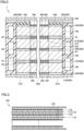
Fig. 1 is a perspective view schematically showing a power storage device according to an embodiment of the present disclosure. -
Fig. 2 is a cross-sectional view taken along line II-II inFig. 1 . -
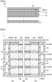
Fig. 3 is a cross-sectional view schematically showing a bipolar electrode. -
Fig. 4 is a cross-sectional view schematically showing a monopolar electrode. -
Fig. 5 is a cross-sectional view schematically showing a modification of the power storage device. -
Fig. 6 is a perspective view schematically showing a modification of a restraint member. - An embodiment of the present disclosure will be described with reference to the drawings. In the drawings referenced below, the same or corresponding members are denoted by the same reference numerals.
-
Fig. 1 is a perspective view schematically showing a power storage device according to an embodiment of the present disclosure.Fig. 2 is a cross-sectional view taken along line II-II inFig. 1 . As shown inFigs. 1 and2 , apower storage device 1 includes a plurality ofpower storage modules 100, a plurality ofconductive members 200, a pair ofrestraint members 300, anadhesive member 400, and anelastic member 500. - The plurality of
power storage modules 100 are stacked on top of each other. In the example shown inFig. 2 , the plurality ofpower storage modules 100 include fourpower storage modules 100. Eachpower storage module 100 is formed to have a rectangular outer shape in a plan view. Eachpower storage module 100 includes a plurality of stacked electrodes. - Each electrode may be implemented by a
bipolar electrode 110 shown inFig. 3 .Bipolar electrode 110 includes a current-collecting foil 111, a positive electrodeactive material layer 112 provided on one surface of current-collecting foil 111, and a negative electrodeactive material layer 113 provided on the other surface of current-collecting foil 111. In this case,power storage module 100 is formed by alternately stackingbipolar electrode 110 and aseparator 130. - Alternatively, each electrode may be implemented by a
monopolar electrode 120 shown inFig. 4 . Positive electrodemonopolar electrode 120 or negative electrodemonopolar electrode 120 includes a current-collecting foil 121, and anactive material layer 122 provided on current-collecting foil 121. In this case,power storage module 100 is formed by stacking positive electrodemonopolar electrode 120 and negative electrodemonopolar electrode 120 withseparator 130 interposed therebetween. - As shown in
Figs. 2 to 4 , an outermost surface of eachpower storage module 100 in a stacking direction of the plurality of electrodes is formed by the electrode. - Each
conductive member 200 is provided between a pair ofpower storage modules 100 adjacent to each other. Eachconductive member 200 brings the pair ofpower storage modules 100 into conduction. In the example shown inFig. 2 , the plurality ofconductive members 200 include fiveconductive members 200. In the present embodiment, the plurality ofconductive members 200 include twocoolers 210 and three current-carrying plates 220. - Each
cooler 210 is arranged betweenpower storage module 100 arranged on the outermost side in the stacking direction (vertical direction inFig. 2 ) of the plurality ofpower storage modules 100, of the plurality ofpower storage modules 100, andpower storage module 100 adjacent to thatpower storage module 100. A flow path through which a coolant (such as water) can flow is provided incooler 210. - Current-
carrying plates 220 are arranged below lowermostpower storage module 100, above uppermostpower storage module 100, and between secondpower storage module 100 from the bottom and thirdpower storage module 100 from the bottom. Each current-carryingplate 220 may be formed to have a flat plate shape. - The pair of
restraint members 300 restrain the plurality ofpower storage modules 100 andconductive members 200 from both sides in the stacking direction. The pair ofrestraint members 300 include alower restraint member 310 and anupper restraint member 320. -
Lower restraint member 310 supports the plurality ofpower storage modules 100 from the bottom. In the present embodiment,lower restraint member 310 is formed by a bottom portion of alower case 315 that houses the plurality ofpower storage modules 100. An outer shape of the bottom portion in a plan view is greater than an outer shape ofpower storage modules 100 in a plan view. As shown inFig. 2 ,power storage device 1 includes anupper case 330 that houses the plurality ofpower storage modules 100, together withlower case 315.Upper case 330 is not shown inFig. 1 . -
Upper restraint member 320 is arranged above the plurality ofpower storage modules 100.Upper restraint member 320 restrains a peripheral edge portion of the plurality ofpower storage modules 100 in a plan view. As shown inFig. 1 ,upper restraint member 320 is formed to have a rectangular ring shape. - As shown in
Fig. 2 , the plurality ofpower storage modules 100 include an overlapping region R10 and a non-overlapping region R20. Overlapping region R10 is a region that overlaps with the pair ofrestraint members 300 in the stacking direction. In the present embodiment, overlapping region R10 is formed by a region that substantially overlaps withupper restraint member 320 in the stacking direction. Non-overlapping region R20 is a region that does not overlap with the pair ofrestraint members 300 in the stacking direction. InFig. 2 , overlapping region R10 is indicated by a dashed-and-dotted line, and non-overlapping region R20 is indicated by a dashed-and-double-dotted line. - In the present embodiment,
cooler 210 includes acentral portion 212 formed in non-overlapping region R20. Current-carrying plate 220 includes acentral portion 222 formed in non-overlapping region R20. -
Adhesive member 400 bondspower storage module 100 andconductive member 200.Adhesive member 400 may be made of a conductive adhesive, or may be made of an insulating adhesive. -
Elastic member 500 is provided betweenpower storage module 100 arranged on the outermost side in the stacking direction, of the plurality ofpower storage modules 100, and at least one of the pair ofrestraint members 300. As shown inFig. 2 ,elastic member 500 is provided between uppermostpower storage module 100 andupper restraint member 320. More specifically,elastic member 500 is provided between current-carryingplate 220 on uppermostpower storage module 100 andupper restraint member 320. It is preferable thatelastic member 500 should be formed to have such a shape thatelastic member 500 is housed in overlapping region R10. - As shown in
Fig. 2 , eachpower storage module 100 includes a direct contact region R1 and an indirect contact region R2. Direct contact region R1 is a region ofpower storage module 100 that is in direct contact withconductive member 200. Indirect contact region R2 is a region ofpower storage module 100 that is in contact withpower storage module 100 adjacent to thatpower storage module 100 orconductive member 200, withadhesive member 400 interposed therebetween. - Overlapping region R10 includes direct contact region R1. In the present embodiment, overlapping region R10 includes only direct contact region R1. However, overlapping region R10 may include a part of indirect contact region R2. Alternatively, a part of direct contact region R1 may be formed in non-overlapping region R20.
- Non-overlapping region R20 includes indirect contact region R2. In the present embodiment, non-overlapping region R20 includes only indirect contact region R2. However, non-overlapping region R20 may include a part of direct contact region R1. Alternatively, a part of indirect contact region R2 may be formed in overlapping region R10.
- As described above, in
power storage device 1 according to the present embodiment, non-overlapping region R20 is provided, and thus, the mass ofrestraint members 300 is reduced and the outer shape ofpower storage device 1 as a whole is also reduced. Furthermore, since overlapping region R10 includes direct contact region R1, electrical conduction between a pair ofpower storage modules 100 adjacent to each other is ensured. In addition, since non-overlapping region R20 includes indirect contact region R2, a pair ofpower storage modules 100 adjacent to each other are effectively fixed. - In the above-described embodiment, as shown in
Fig. 5 ,conductive member 200 does not necessarily includecentral portions power storage modules 100 adjacent to each other are in contact with each other withadhesive member 400 interposed therebetween. - In addition, as shown in
Fig. 6 , the pair ofrestraint members 300 may restrain four corners of eachpower storage module 100. - It is understood by those skilled in the art that the illustrative embodiment and example described above are specific examples of the following aspects.
- A power storage device comprising:
- a plurality of power storage modules stacked on top of each other, each of the plurality of power storage modules including a plurality of stacked electrodes;
- a conductive member provided between a pair of the power storage modules adjacent to each other, to bring the pair of the power storage modules into conduction;
- a pair of restraint members that restrain the plurality of power storage modules and the conductive member from both sides in a stacking direction of the plurality of power storage modules; and
- an adhesive member that bonds the power storage module and the conductive member, wherein
- the plurality of power storage modules include:
- an overlapping region that overlaps with the pair of restraint members in the stacking direction; and
- a non-overlapping region that does not overlap with the pair of restraint members in the stacking direction,
- each power storage module includes:
- a direct contact region that is in direct contact with the conductive member; and
- an indirect contact region that is in contact with the power storage module adjacent to that power storage module or the conductive member, with the adhesive member interposed therebetween,
- the overlapping region includes the direct contact region, and
- the non-overlapping region includes the indirect contact region.
- In this power storage device, the non-overlapping region is provided, and thus, the mass of the restraint members and the outer shape of the power storage device as a whole can be reduced. Furthermore, since the overlapping region includes the direct contact region, electrical conduction between a pair of power storage modules adjacent to each other is ensured. In addition, since the non-overlapping region includes the indirect contact region, a pair of power storage modules adjacent to each other are effectively fixed.
- The power storage device according to
Aspect 1, wherein
the overlapping region includes only the direct contact region. - In this aspect, electrical conduction between a pair of power storage modules adjacent to each other is ensured more reliably.
- The power storage device according to
Aspect 1 or 2, wherein
the pair of restraint members restrain a peripheral edge portion of the plurality of power storage modules in a plan view. - In this aspect, even when each power storage module increases in area, the mass of the restraint members and the outer shape of the power storage device as a whole are reduced.
- The power storage device according to
Aspect 1 or 2, wherein - each power storage module is formed to have a rectangular shape in a plan view, and
- the pair of restraint members restrain four corners of each power storage module.
- In this aspect, even when each power storage module increases in area, the mass of the restraint members and the outer shape of the power storage device as a whole are reduced.
- The power storage device according to any one of
Aspects 1 to 4, further comprising
an elastic member provided between a power storage module arranged on an outermost side in the stacking direction, of the plurality of power storage modules, and at least one of the pair of restraint members. - In this aspect, a restraining load applied by the restraint members can be adjusted by the elastic member.
- Although the embodiment of the present disclosure has been described, it should be understood that the embodiment disclosed herein is illustrative and non-restrictive in every respect. The scope of the present disclosure is defined by the terms of the claims and is intended to include any modifications within the scope and meaning equivalent to the terms of the claims.
Claims (5)
- A power storage device (1) comprising:a plurality of power storage modules (100) stacked on top of each other, each of the plurality of power storage modules including a plurality of stacked electrodes (110, 120);a conductive member (200) provided between a pair of the power storage modules adjacent to each other, to bring the pair of the power storage modules into conduction;a pair of restraint members (300) that restrain the plurality of power storage modules and the conductive member from both sides in a stacking direction of the plurality of power storage modules; andan adhesive member (400) that bonds the power storage module and the conductive member, whereinthe plurality of power storage modules include:an overlapping region (R10) that overlaps with the pair of restraint members in the stacking direction; anda non-overlapping region (R20) that does not overlap with the pair of restraint members in the stacking direction,each power storage module includes:a direct contact region (R1) that is in direct contact with the conductive member; andan indirect contact region (R2) that is in contact with the power storage module adjacent to that power storage module or the conductive member, with the adhesive member interposed therebetween,the overlapping region (R10) includes the direct contact region (R1), andthe non-overlapping region (R20) includes the indirect contact region (R2).
- The power storage device according to claim 1, wherein
the overlapping region (R10) includes only the direct contact region (R1). - The power storage device according to claim 1 or 2, wherein
the pair of restraint members (300) restrain a peripheral edge portion of the plurality of power storage modules in a plan view. - The power storage device according to claim 1 or 2, whereineach power storage module is formed to have a rectangular shape in a plan view, andthe pair of restraint members restrain four corners of each power storage module.
- The power storage device according to claim 1, further comprising
an elastic member (500) provided between a power storage module arranged on an outermost side in the stacking direction, of the plurality of power storage modules, and at least one of the pair of restraint members.
Applications Claiming Priority (1)
| Application Number | Priority Date | Filing Date | Title |
|---|---|---|---|
| JP2023019210A JP7643477B2 (en) | 2023-02-10 | 2023-02-10 | Power storage device |
Publications (4)
| Publication Number | Publication Date |
|---|---|
| EP4425660A2 true EP4425660A2 (en) | 2024-09-04 |
| EP4425660A3 EP4425660A3 (en) | 2024-12-25 |
| EP4425660B1 EP4425660B1 (en) | 2025-10-22 |
| EP4425660C0 EP4425660C0 (en) | 2025-10-22 |
Family
ID=89767012
Family Applications (1)
| Application Number | Title | Priority Date | Filing Date |
|---|---|---|---|
| EP24154196.0A Active EP4425660B1 (en) | 2023-02-10 | 2024-01-26 | Power storage device |
Country Status (5)
| Country | Link |
|---|---|
| US (1) | US20240274959A1 (en) |
| EP (1) | EP4425660B1 (en) |
| JP (1) | JP7643477B2 (en) |
| KR (1) | KR102880188B1 (en) |
| CN (1) | CN118486967A (en) |
Cited By (1)
| Publication number | Priority date | Publication date | Assignee | Title |
|---|---|---|---|---|
| EP4723302A1 (en) * | 2024-10-01 | 2026-04-08 | Toyota Jidosha Kabushiki Kaisha | Power storage device |
Citations (1)
| Publication number | Priority date | Publication date | Assignee | Title |
|---|---|---|---|---|
| JP2019216073A (en) | 2018-06-14 | 2019-12-19 | 株式会社豊田自動織機 | Manufacturing method for power storage device and power storage device |
Family Cites Families (6)
| Publication number | Priority date | Publication date | Assignee | Title |
|---|---|---|---|---|
| GB2584344A (en) * | 2019-05-31 | 2020-12-02 | Oxis Energy Ltd | Battery cell |
| WO2021095551A1 (en) * | 2019-11-13 | 2021-05-20 | 株式会社豊田自動織機 | Electrical storage device |
| JP7468233B2 (en) * | 2020-07-31 | 2024-04-16 | 株式会社豊田自動織機 | Energy Storage Module |
| CN218070041U (en) * | 2021-07-06 | 2022-12-16 | 芜湖天弋能源科技有限公司 | Long circulation lithium cell group package assembly |
| CN214706146U (en) * | 2021-10-18 | 2021-11-12 | 嘉兴模度新能源有限公司 | Self-tightening type battery pack and battery pack |
| CN218385535U (en) * | 2022-08-24 | 2023-01-24 | 芜湖天弋能源科技有限公司 | Power battery module structure |
-
2023
- 2023-02-10 JP JP2023019210A patent/JP7643477B2/en active Active
-
2024
- 2024-01-12 US US18/411,862 patent/US20240274959A1/en active Pending
- 2024-01-26 EP EP24154196.0A patent/EP4425660B1/en active Active
- 2024-02-05 KR KR1020240017542A patent/KR102880188B1/en active Active
- 2024-02-08 CN CN202410175659.4A patent/CN118486967A/en active Pending
Patent Citations (1)
| Publication number | Priority date | Publication date | Assignee | Title |
|---|---|---|---|---|
| JP2019216073A (en) | 2018-06-14 | 2019-12-19 | 株式会社豊田自動織機 | Manufacturing method for power storage device and power storage device |
Cited By (1)
| Publication number | Priority date | Publication date | Assignee | Title |
|---|---|---|---|---|
| EP4723302A1 (en) * | 2024-10-01 | 2026-04-08 | Toyota Jidosha Kabushiki Kaisha | Power storage device |
Also Published As
| Publication number | Publication date |
|---|---|
| EP4425660B1 (en) | 2025-10-22 |
| JP7643477B2 (en) | 2025-03-11 |
| JP2024113927A (en) | 2024-08-23 |
| CN118486967A (en) | 2024-08-13 |
| KR20240125452A (en) | 2024-08-19 |
| EP4425660C0 (en) | 2025-10-22 |
| US20240274959A1 (en) | 2024-08-15 |
| KR102880188B1 (en) | 2025-11-04 |
| EP4425660A3 (en) | 2024-12-25 |
Similar Documents
| Publication | Publication Date | Title |
|---|---|---|
| JP5825436B2 (en) | ELECTRODE ASSEMBLY EXCELLENT IN ELECTRODE TAB CONNECTIVITY, BATTERY CELL CONTAINING THE SAME, DEVICE AND MANUFACTURING METHOD | |
| KR200207948Y1 (en) | Lithium ion polymer battery | |
| KR102931321B1 (en) | Battery Module and Battery Pack Having The Same | |
| EP3391430B1 (en) | Through-wall current collector for a pouch cell | |
| KR102788645B1 (en) | Battery Pack | |
| EP3211688B1 (en) | Rechargeable battery | |
| US20250153262A1 (en) | Welding Apparatus and Welding Method | |
| EP4425660A2 (en) | Power storage device | |
| KR102769533B1 (en) | Rechargeable secondary battery | |
| US20230216146A1 (en) | Battery pack connector | |
| EP4415080A1 (en) | Power storage device | |
| KR20250176856A (en) | Battery device | |
| KR102807655B1 (en) | Secondary battery | |
| EP4683004A1 (en) | Electrode plate, stacked-type cell, and pouch battery | |
| KR20250176861A (en) | Battery device | |
| US20240178492A1 (en) | Power storage module | |
| JP2009188115A (en) | Electrical double-layer capacitor | |
| US20250158201A1 (en) | Power storage device | |
| KR20260059064A (en) | Battery pack | |
| KR20260036687A (en) | Battery device | |
| KR20250171940A (en) | Battery device | |
| KR20260037229A (en) | Electrode assembly and secondary battery comprising the same | |
| KR20250118584A (en) | Battery pack | |
| JP2024141456A (en) | Battery Cells and Modules | |
| KR20260022126A (en) | Transport device and method of manufaturing secondary battery using the same |
Legal Events
| Date | Code | Title | Description |
|---|---|---|---|
| PUAI | Public reference made under article 153(3) epc to a published international application that has entered the european phase |
Free format text: ORIGINAL CODE: 0009012 |
|
| STAA | Information on the status of an ep patent application or granted ep patent |
Free format text: STATUS: REQUEST FOR EXAMINATION WAS MADE |
|
| 17P | Request for examination filed |
Effective date: 20240208 |
|
| AK | Designated contracting states |
Kind code of ref document: A2 Designated state(s): AL AT BE BG CH CY CZ DE DK EE ES FI FR GB GR HR HU IE IS IT LI LT LU LV MC ME MK MT NL NO PL PT RO RS SE SI SK SM TR |
|
| REG | Reference to a national code |
Ref country code: DE Ref legal event code: R079 Free format text: PREVIOUS MAIN CLASS: H01M0050209000 Ipc: H01M0050264000 Ref document number: 602024000970 Country of ref document: DE |
|
| PUAL | Search report despatched |
Free format text: ORIGINAL CODE: 0009013 |
|
| AK | Designated contracting states |
Kind code of ref document: A3 Designated state(s): AL AT BE BG CH CY CZ DE DK EE ES FI FR GB GR HR HU IE IS IT LI LT LU LV MC ME MK MT NL NO PL PT RO RS SE SI SK SM TR |
|
| RIC1 | Information provided on ipc code assigned before grant |
Ipc: H01G 11/76 20130101ALN20241121BHEP Ipc: H01M 50/514 20210101ALI20241121BHEP Ipc: H01G 11/10 20130101ALI20241121BHEP Ipc: H01G 2/02 20060101ALI20241121BHEP Ipc: H01M 50/291 20210101ALI20241121BHEP Ipc: H01M 50/244 20210101ALI20241121BHEP Ipc: H01M 50/209 20210101ALI20241121BHEP Ipc: H01G 11/82 20130101ALI20241121BHEP Ipc: H01M 50/264 20210101AFI20241121BHEP |
|
| GRAP | Despatch of communication of intention to grant a patent |
Free format text: ORIGINAL CODE: EPIDOSNIGR1 |
|
| STAA | Information on the status of an ep patent application or granted ep patent |
Free format text: STATUS: GRANT OF PATENT IS INTENDED |
|
| RIC1 | Information provided on ipc code assigned before grant |
Ipc: H01G 2/10 20060101ALN20250509BHEP Ipc: H01G 11/76 20130101ALN20250509BHEP Ipc: H01G 11/12 20130101ALI20250509BHEP Ipc: H01M 50/514 20210101ALI20250509BHEP Ipc: H01G 11/10 20130101ALI20250509BHEP Ipc: H01G 2/02 20060101ALI20250509BHEP Ipc: H01M 50/291 20210101ALI20250509BHEP Ipc: H01M 50/244 20210101ALI20250509BHEP Ipc: H01M 50/209 20210101ALI20250509BHEP Ipc: H01G 11/82 20130101ALI20250509BHEP Ipc: H01M 50/264 20210101AFI20250509BHEP |
|
| INTG | Intention to grant announced |
Effective date: 20250522 |
|
| GRAS | Grant fee paid |
Free format text: ORIGINAL CODE: EPIDOSNIGR3 |
|
| GRAA | (expected) grant |
Free format text: ORIGINAL CODE: 0009210 |
|
| STAA | Information on the status of an ep patent application or granted ep patent |
Free format text: STATUS: THE PATENT HAS BEEN GRANTED |
|
| AK | Designated contracting states |
Kind code of ref document: B1 Designated state(s): AL AT BE BG CH CY CZ DE DK EE ES FI FR GB GR HR HU IE IS IT LI LT LU LV MC ME MK MT NL NO PL PT RO RS SE SI SK SM TR |
|
| REG | Reference to a national code |
Ref country code: CH Ref legal event code: F10 Free format text: ST27 STATUS EVENT CODE: U-0-0-F10-F00 (AS PROVIDED BY THE NATIONAL OFFICE) Effective date: 20251022 Ref country code: GB Ref legal event code: FG4D |
|
| REG | Reference to a national code |
Ref country code: DE Ref legal event code: R096 Ref document number: 602024000970 Country of ref document: DE |
|
| REG | Reference to a national code |
Ref country code: IE Ref legal event code: FG4D |
|
| U01 | Request for unitary effect filed |
Effective date: 20251106 |
|
| U07 | Unitary effect registered |
Designated state(s): AT BE BG DE DK EE FI FR IT LT LU LV MT NL PT RO SE SI Effective date: 20251112 |
|
| PGFP | Annual fee paid to national office [announced via postgrant information from national office to epo] |
Ref country code: GR Payment date: 20251230 Year of fee payment: 3 |
|
| REG | Reference to a national code |
Ref country code: GR Ref legal event code: EP Ref document number: 20250402424 Country of ref document: GR Effective date: 20260115 |
|
| PGFP | Annual fee paid to national office [announced via postgrant information from national office to epo] |
Ref country code: IE Payment date: 20251223 Year of fee payment: 3 |
|
| U20 | Renewal fee for the european patent with unitary effect paid |
Year of fee payment: 3 Effective date: 20260106 |
|
| PG25 | Lapsed in a contracting state [announced via postgrant information from national office to epo] |
Ref country code: ES Free format text: LAPSE BECAUSE OF FAILURE TO SUBMIT A TRANSLATION OF THE DESCRIPTION OR TO PAY THE FEE WITHIN THE PRESCRIBED TIME-LIMIT Effective date: 20251022 |
|
| PG25 | Lapsed in a contracting state [announced via postgrant information from national office to epo] |
Ref country code: NO Free format text: LAPSE BECAUSE OF FAILURE TO SUBMIT A TRANSLATION OF THE DESCRIPTION OR TO PAY THE FEE WITHIN THE PRESCRIBED TIME-LIMIT Effective date: 20260122 |
|
| PG25 | Lapsed in a contracting state [announced via postgrant information from national office to epo] |
Ref country code: HR Free format text: LAPSE BECAUSE OF FAILURE TO SUBMIT A TRANSLATION OF THE DESCRIPTION OR TO PAY THE FEE WITHIN THE PRESCRIBED TIME-LIMIT Effective date: 20251022 |
|
| PG25 | Lapsed in a contracting state [announced via postgrant information from national office to epo] |
Ref country code: RS Free format text: LAPSE BECAUSE OF FAILURE TO SUBMIT A TRANSLATION OF THE DESCRIPTION OR TO PAY THE FEE WITHIN THE PRESCRIBED TIME-LIMIT Effective date: 20260122 |
|
| PG25 | Lapsed in a contracting state [announced via postgrant information from national office to epo] |
Ref country code: IS Free format text: LAPSE BECAUSE OF FAILURE TO SUBMIT A TRANSLATION OF THE DESCRIPTION OR TO PAY THE FEE WITHIN THE PRESCRIBED TIME-LIMIT Effective date: 20260222 |
|
| PGFP | Annual fee paid to national office [announced via postgrant information from national office to epo] |
Ref country code: TR Payment date: 20260122 Year of fee payment: 3 |
|
| PG25 | Lapsed in a contracting state [announced via postgrant information from national office to epo] |
Ref country code: PL Free format text: LAPSE BECAUSE OF FAILURE TO SUBMIT A TRANSLATION OF THE DESCRIPTION OR TO PAY THE FEE WITHIN THE PRESCRIBED TIME-LIMIT Effective date: 20251022 |
|
| U1N | Appointed representative for the unitary patent procedure changed after the registration of the unitary effect |
Representative=s name: MARKS & CLERK LLP; GB |