EP4425562A2 - Process for manufacturing a power electronic device having a current spreading layer - Google Patents
Process for manufacturing a power electronic device having a current spreading layer Download PDFInfo
- Publication number
- EP4425562A2 EP4425562A2 EP24159349.0A EP24159349A EP4425562A2 EP 4425562 A2 EP4425562 A2 EP 4425562A2 EP 24159349 A EP24159349 A EP 24159349A EP 4425562 A2 EP4425562 A2 EP 4425562A2
- Authority
- EP
- European Patent Office
- Prior art keywords
- process according
- forming
- current spreading
- front surface
- semiconductor body
- Prior art date
- Legal status (The legal status is an assumption and is not a legal conclusion. Google has not performed a legal analysis and makes no representation as to the accuracy of the status listed.)
- Pending
Links
Images

Classifications
-
- H—ELECTRICITY
- H10—SEMICONDUCTOR DEVICES; ELECTRIC SOLID-STATE DEVICES NOT OTHERWISE PROVIDED FOR
- H10P—GENERIC PROCESSES OR APPARATUS FOR THE MANUFACTURE OR TREATMENT OF DEVICES COVERED BY CLASS H10
- H10P30/00—Ion implantation into wafers, substrates or parts of devices
- H10P30/20—Ion implantation into wafers, substrates or parts of devices into semiconductor materials, e.g. for doping
- H10P30/21—Ion implantation into wafers, substrates or parts of devices into semiconductor materials, e.g. for doping of electrically active species
-
- H—ELECTRICITY
- H10—SEMICONDUCTOR DEVICES; ELECTRIC SOLID-STATE DEVICES NOT OTHERWISE PROVIDED FOR
- H10D—INORGANIC ELECTRIC SEMICONDUCTOR DEVICES
- H10D62/00—Semiconductor bodies, or regions thereof, of devices having potential barriers
- H10D62/80—Semiconductor bodies, or regions thereof, of devices having potential barriers characterised by the materials
- H10D62/83—Semiconductor bodies, or regions thereof, of devices having potential barriers characterised by the materials being Group IV materials, e.g. B-doped Si or undoped Ge
- H10D62/832—Semiconductor bodies, or regions thereof, of devices having potential barriers characterised by the materials being Group IV materials, e.g. B-doped Si or undoped Ge being Group IV materials comprising two or more elements, e.g. SiGe
- H10D62/8325—Silicon carbide
-
- H—ELECTRICITY
- H10—SEMICONDUCTOR DEVICES; ELECTRIC SOLID-STATE DEVICES NOT OTHERWISE PROVIDED FOR
- H10D—INORGANIC ELECTRIC SEMICONDUCTOR DEVICES
- H10D12/00—Bipolar devices controlled by the field effect, e.g. insulated-gate bipolar transistors [IGBT]
- H10D12/01—Manufacture or treatment
- H10D12/031—Manufacture or treatment of IGBTs
-
- H—ELECTRICITY
- H10—SEMICONDUCTOR DEVICES; ELECTRIC SOLID-STATE DEVICES NOT OTHERWISE PROVIDED FOR
- H10D—INORGANIC ELECTRIC SEMICONDUCTOR DEVICES
- H10D30/00—Field-effect transistors [FET]
- H10D30/01—Manufacture or treatment
- H10D30/021—Manufacture or treatment of FETs having insulated gates [IGFET]
- H10D30/028—Manufacture or treatment of FETs having insulated gates [IGFET] of double-diffused metal oxide semiconductor [DMOS] FETs
- H10D30/0291—Manufacture or treatment of FETs having insulated gates [IGFET] of double-diffused metal oxide semiconductor [DMOS] FETs of vertical DMOS [VDMOS] FETs
-
- H—ELECTRICITY
- H10—SEMICONDUCTOR DEVICES; ELECTRIC SOLID-STATE DEVICES NOT OTHERWISE PROVIDED FOR
- H10D—INORGANIC ELECTRIC SEMICONDUCTOR DEVICES
- H10D30/00—Field-effect transistors [FET]
- H10D30/60—Insulated-gate field-effect transistors [IGFET]
- H10D30/64—Double-diffused metal-oxide semiconductor [DMOS] FETs
- H10D30/66—Vertical DMOS [VDMOS] FETs
-
- H—ELECTRICITY
- H10—SEMICONDUCTOR DEVICES; ELECTRIC SOLID-STATE DEVICES NOT OTHERWISE PROVIDED FOR
- H10D—INORGANIC ELECTRIC SEMICONDUCTOR DEVICES
- H10D30/00—Field-effect transistors [FET]
- H10D30/60—Insulated-gate field-effect transistors [IGFET]
- H10D30/64—Double-diffused metal-oxide semiconductor [DMOS] FETs
- H10D30/66—Vertical DMOS [VDMOS] FETs
- H10D30/662—Vertical DMOS [VDMOS] FETs having a drift region having a doping concentration that is higher between adjacent body regions relative to other parts of the drift region
-
- H—ELECTRICITY
- H10—SEMICONDUCTOR DEVICES; ELECTRIC SOLID-STATE DEVICES NOT OTHERWISE PROVIDED FOR
- H10D—INORGANIC ELECTRIC SEMICONDUCTOR DEVICES
- H10D62/00—Semiconductor bodies, or regions thereof, of devices having potential barriers
- H10D62/10—Shapes, relative sizes or dispositions of the regions of the semiconductor bodies; Shapes of the semiconductor bodies
- H10D62/102—Constructional design considerations for preventing surface leakage or controlling electric field concentration
- H10D62/103—Constructional design considerations for preventing surface leakage or controlling electric field concentration for increasing or controlling the breakdown voltage of reverse-biased devices
- H10D62/105—Constructional design considerations for preventing surface leakage or controlling electric field concentration for increasing or controlling the breakdown voltage of reverse-biased devices by having particular doping profiles, shapes or arrangements of PN junctions; by having supplementary regions, e.g. junction termination extension [JTE]
- H10D62/106—Constructional design considerations for preventing surface leakage or controlling electric field concentration for increasing or controlling the breakdown voltage of reverse-biased devices by having particular doping profiles, shapes or arrangements of PN junctions; by having supplementary regions, e.g. junction termination extension [JTE] having supplementary regions doped oppositely to or in rectifying contact with regions of the semiconductor bodies, e.g. guard rings with PN or Schottky junctions
-
- H—ELECTRICITY
- H10—SEMICONDUCTOR DEVICES; ELECTRIC SOLID-STATE DEVICES NOT OTHERWISE PROVIDED FOR
- H10D—INORGANIC ELECTRIC SEMICONDUCTOR DEVICES
- H10D62/00—Semiconductor bodies, or regions thereof, of devices having potential barriers
- H10D62/10—Shapes, relative sizes or dispositions of the regions of the semiconductor bodies; Shapes of the semiconductor bodies
- H10D62/13—Semiconductor regions connected to electrodes carrying current to be rectified, amplified or switched, e.g. source or drain regions
- H10D62/149—Source or drain regions of field-effect devices
- H10D62/151—Source or drain regions of field-effect devices of IGFETs
- H10D62/156—Drain regions of DMOS transistors
- H10D62/157—Impurity concentrations or distributions
-
- H—ELECTRICITY
- H10—SEMICONDUCTOR DEVICES; ELECTRIC SOLID-STATE DEVICES NOT OTHERWISE PROVIDED FOR
- H10D—INORGANIC ELECTRIC SEMICONDUCTOR DEVICES
- H10D62/00—Semiconductor bodies, or regions thereof, of devices having potential barriers
- H10D62/10—Shapes, relative sizes or dispositions of the regions of the semiconductor bodies; Shapes of the semiconductor bodies
- H10D62/17—Semiconductor regions connected to electrodes not carrying current to be rectified, amplified or switched, e.g. channel regions
- H10D62/213—Channel regions of field-effect devices
- H10D62/221—Channel regions of field-effect devices of FETs
- H10D62/235—Channel regions of field-effect devices of FETs of IGFETs
- H10D62/292—Non-planar channels of IGFETs
-
- H—ELECTRICITY
- H10—SEMICONDUCTOR DEVICES; ELECTRIC SOLID-STATE DEVICES NOT OTHERWISE PROVIDED FOR
- H10D—INORGANIC ELECTRIC SEMICONDUCTOR DEVICES
- H10D62/00—Semiconductor bodies, or regions thereof, of devices having potential barriers
- H10D62/10—Shapes, relative sizes or dispositions of the regions of the semiconductor bodies; Shapes of the semiconductor bodies
- H10D62/17—Semiconductor regions connected to electrodes not carrying current to be rectified, amplified or switched, e.g. channel regions
- H10D62/393—Body regions of DMOS transistors or IGBTs
-
- H—ELECTRICITY
- H10—SEMICONDUCTOR DEVICES; ELECTRIC SOLID-STATE DEVICES NOT OTHERWISE PROVIDED FOR
- H10D—INORGANIC ELECTRIC SEMICONDUCTOR DEVICES
- H10D62/00—Semiconductor bodies, or regions thereof, of devices having potential barriers
- H10D62/40—Crystalline structures
- H10D62/405—Orientations of crystalline planes
-
- H—ELECTRICITY
- H10—SEMICONDUCTOR DEVICES; ELECTRIC SOLID-STATE DEVICES NOT OTHERWISE PROVIDED FOR
- H10P—GENERIC PROCESSES OR APPARATUS FOR THE MANUFACTURE OR TREATMENT OF DEVICES COVERED BY CLASS H10
- H10P30/00—Ion implantation into wafers, substrates or parts of devices
- H10P30/20—Ion implantation into wafers, substrates or parts of devices into semiconductor materials, e.g. for doping
- H10P30/202—Ion implantation into wafers, substrates or parts of devices into semiconductor materials, e.g. for doping characterised by the semiconductor materials
- H10P30/204—Ion implantation into wafers, substrates or parts of devices into semiconductor materials, e.g. for doping characterised by the semiconductor materials into Group IV semiconductors
- H10P30/2042—Ion implantation into wafers, substrates or parts of devices into semiconductor materials, e.g. for doping characterised by the semiconductor materials into Group IV semiconductors into crystalline silicon carbide
-
- H—ELECTRICITY
- H10—SEMICONDUCTOR DEVICES; ELECTRIC SOLID-STATE DEVICES NOT OTHERWISE PROVIDED FOR
- H10P—GENERIC PROCESSES OR APPARATUS FOR THE MANUFACTURE OR TREATMENT OF DEVICES COVERED BY CLASS H10
- H10P30/00—Ion implantation into wafers, substrates or parts of devices
- H10P30/20—Ion implantation into wafers, substrates or parts of devices into semiconductor materials, e.g. for doping
- H10P30/222—Ion implantation into wafers, substrates or parts of devices into semiconductor materials, e.g. for doping characterised by the angle between the ion beam and the crystal planes or the main crystal surface
Definitions
- the present solution relates to a process for manufacturing a power electronic device, having a current spreading layer, CSL; in particular, the following discussion will make particular reference to a power electronic device formed starting from a silicon-carbide, SiC, substrate.
- semiconductor materials having a wide bandgap, for example greater than 1.1 eV, low on-state resistance, high thermal conductivity, high operating frequency and high saturation velocity of the charge carriers allow manufacturing of electronic devices, for example diodes and transistors, which may have better performances than silicon electronic devices, in particular for power applications, for example with operating voltages comprised between 600 V and 1300 V and/or specific operating conditions such as high temperature.
- these power electronic devices may advantageously be formed starting from a wafer of silicon carbide, a material which has the characteristics listed above, in one of its polytypes, for example 3C-SiC, 4H-SiC and 6H-SiC.
- power electronic devices may include a current spreading layer, CSL, having a suitable doping, in order to locally modulate the resistivity of the silicon-carbide substrate, causing the injected current to spread in a uniform manner across an area of the same substrate.
- CSL current spreading layer
- the CSL layer may be used in the intercell (or JFET) region to reduce the on-state resistance (R on ).
- the process for manufacturing such power electronic devices therefore comprises, typically in an initial step, formation of the current spreading layer by a dedicated epitaxial growth, performed starting from the substrate, for example of silicon carbide.
- the formation of a thick epitaxial layer is required, so that, typically, at least two epitaxial growths are required to reach the desired thickness.
- This manufacturing process entails times and costs which are quite high, due to the need to implement the control of the process recipe and parameters to implement a second epitaxial growth, independently of, and in addition to, a first epitaxial growth.
- the present solution has the aim of solving, at least in part, the previously highlighted issues, providing an alternative process for manufacturing of the current spreading layer in a power electronic device, in particular of silicon carbide, which offers a simpler and cheaper implementation.
- one aspect of the present solution envisages formation of a current spreading layer (CSL layer) in a power electronic device, in particular made of silicon carbide, by a channeled ion implantation process (in a so-called "channeling" condition).
- CSL layer current spreading layer
- the channeling condition occurs when the direction of the implanted ion beam is oriented along one of the semiconductor material crystallographic axes, substantially parallel thereto.
- the ions When implanted in the crystal lattice, the ions generally tend to disperse due to impacts with the atoms of the crystal lattice (according to the phenomenon of impact scattering).
- the implant direction When the implant direction is oriented to an oblique angle with respect to the main axes of the crystal lattice, the atoms in the lattice have a random distribution with respect to the implant direction; the probability of collisions between the implanted ions and the atoms of the crystal lattice is therefore substantially uniform as the depth varies. Therefore, in this implant condition, doping profiles, which are substantially Gaussian with respect to the depth, are obtained, where the depth reached by the implant is determined by the energy, the ions used and the atomic structure of the target.
- the implant direction is instead a channeling direction, close to a main axis of the crystal lattice, the atoms in the crystal lattice define "channels" that may be traversed by the implanted ions. This reduces the probability of collisions between the implanted ions and the atoms of the crystal lattice, especially near the surface of the wafer wherein the implant occurs, resulting in that the depth of the same implant may be significantly increased.
- the implant channeling occurs when the implant direction is within a critical angle with respect to the channeling direction.
- the loss of electron energy (interaction with the electron clouds of the crystal atoms) is prevalent with respect to the nuclear loss (impacts with the crystal nuclei).
- the value of the critical angle depends for example on the direction, the species and the energy used.
- the term "implant angle” refers to the tilt angle of the wafer during the implant. It may be defined in general as angle with respect to the surface of the wafer. In general, the surface of the wafer is not a crystallographic plane, as it is defined by a cut angle suitable for subsequent epitaxial processes, for example 4°; in the example, therefore, to identify the ⁇ 0001> direction of the crystal lattice during the implant, the wafer needs to be tilted with a tilt angle of 4°.
- Channeling is typically an undesired effect during manufacturing of power electronic devices (for example, because the implant depth may be greater than the desired depth and because it is difficult to control the value of the same depth) and the implant direction is therefore generally oriented in a non-channeling direction, to minimize channeling effects.
- the present Applicant has however realized the possibility of providing, in a controlled and repeatable manner, channeled implants within the process for manufacturing a silicon-carbide power electronic device, in particular for forming a corresponding current spreading layer.
- a first embodiment of the present solution initially envisages the provision of a wafer 1 comprising a substrate 2 of silicon carbide, for example of 4H-SiC-type having a doping with n-type conductivity (for example with a dose of the order of 5e 18 ions cm -3 ), and delimited by a front surface 1a and a rear surface 1b, having a main extension in a horizontal plane xy and opposite to each other along a vertical axis z, orthogonal to the horizontal plane xy.
- drift layer 4 is then formed for forming a drift layer 4 on the substrate 2, also having a n-type conductivity, for example n - (with a dose of the order of 5e 15 ions cm -3 ); this drift layer 4 therefore defines the front surface 1a of the wafer 1.
- the silicon carbide crystallographic lattice is oriented at a certain angle (non-zero) with respect to the surface of the wafer 1.
- the 4H-SiC lattice structure has an off-cut angle of about 4° (intended as the angle between the surface of the wafer 1 and the main crystallographic plane, for example along the ⁇ 0001> direction).
- a blank implant is then performed in the active area in channeling condition for forming a current spreading layer (CSL) 6, continuous and seamless, in proximity of the front surface 1a of the wafer 1, having n-type conductivity and greater doping than that of the drift layer 4 (thus operating as an enrichment layer).
- CSL current spreading layer
- the implant is performed at a certain angle (tilt angle) with respect to a direction orthogonal to the front surface 1a of the wafer 1, in such a way as to provide the channeling conditions and thus allow the channeling of the implanted ions towards the depth of the drift layer 4.
- the ion implant may be performed with a tilt angle comprised between 3.5° and 4.5°, for example equal to about 4°, in such a way that the implantation occurs substantially in a channeled manner along the ⁇ 0001> direction of the crystal lattice.
- the implant dose may be for example of about 8 ⁇ 10 12 ions cm -2 (nominal) and the implantation may be performed at room temperature.
- Figure 2 shows the implant profile (i.e. the implant dose as a function of the depth in the drift layer 4 along the vertical axis z) in two different conditions: with an implantation performed in channeling condition, in the example with tilt angle equal to 4° (profile shown in solid line); and with an implantation with a direction orthogonal to the surface, with a substantially zero tilt angle (profile shown in dashed line).
- an implantation performed in channeling condition in the example with tilt angle equal to 4° (profile shown in solid line); and with an implantation with a direction orthogonal to the surface, with a substantially zero tilt angle (profile shown in dashed line).
- the channeled implant allows a substantially flat doping profile to be obtained, within a desired depth of the current spreading layer 6 starting from the front surface 1a of the wafer 1 (this depth being for example comprised between 0.5 and 5 ⁇ m, for example equal to 2 ⁇ m).
- the present Applicant has experimentally demonstrated that the discussed channeled ion implantation allows a very precise control of the doping of the current spreading layer 6, in particular with variations lower than 1% with respect to a desired value (in this regard, in case of epitaxial manufacturing of the same current spreading layer, typical doping variations of the order of 10% are obtained).
- the aforementioned channeled ion implantation allows very precise control of the depth of the current spreading layer 6, in particular with variations lower than 1% with respect to a desired value (in this regard, in case of epitaxial manufacturing of the same current spreading layer typical depth variations of the order of 10% are obtained).
- the manufacturing process then proceeds with the formation, in the active area, of elementary cells of the power electronic device.
- Body regions 10 are then initially formed within the drift layer 4 and in particular within the current spreading layer 6, that was previously formed, at the front surface 1a of the wafer 1, by a masked implantation of p-type doping ions (this implantation being performed in a traditional manner, i.e. with a random ion implant, with a substantially zero tilt angle).
- the body regions 10 are separated at a certain distance from each other along a x axis of the horizontal plane xy; in particular, the portions of the drift layer 4 between adjacent body regions 10, at the front surface 1a, are defined as intercell or JFET regions and are indicated by 11.
- respective source regions 12 are formed, again by masked ion implantation, in this case of n-type (for example with nitrogen or phosphorus ions), within each body region 10 (centrally with respect thereto). These source regions 12 have a depth along the vertical axis z smaller than a corresponding depth of the same body regions 10.
- the wafer 1 may be subjected to annealing for activating the doping ions and for reducing the defects in the crystal lattice.
- body contact regions 14 are formed within some of the source regions 12 (centrally with respect thereto) and at the front surface 1a of the wafer 1.
- a body contact region 14 may be formed every two source regions 12.
- These body contact regions 14, which have the purpose of creating an ohmic contact with the respective body regions 10, are formed again by masked ion implant, in this case of p + type with a high doping dose (for example comprised between 10 14 and 5 ⁇ 10 15 ions cm -2 ), and suitable energy (for example comprised between 10 keV and 300 keV).
- a high doping dose for example comprised between 10 14 and 5 ⁇ 10 15 ions cm -2
- suitable energy for example comprised between 10 keV and 300 keV.
- the wafer 1 is processed in a known manner, forming insulated gate structures 16 on the front surface 1a of the wafer 1 and a source metallization region 18.
- these insulated gate regions 16 are each formed by: a gate insulating region 20, for example of oxide, in contact with the front surface 1a of the wafer 1, above the aforementioned JFET region 11; a gate conductive region 21, directly superimposed on the gate insulating region 20, of a conductive material; and a passivation region 22, covering the gate conductive region 21 and sealing, together with the gate insulating region 20, the gate conductive region 21.
- the gate conductive regions 21 of the insulated gate structures 16 are electrically connected in parallel, in a manner not shown here, forming a gate terminal of the MOSFET power electronic device.
- the source metallization region 18 for example of metal material and/or metal silicide, forms a source terminal of the MOSFET power electronic device and extends over the first surface 1a of the wafer and over the insulated gate structures 16, in direct electrical contact with the source regions 12 and the body contact regions 14.
- a further metallization region may be formed on the rear surface 1b of the wafer 1, to form a drain terminal of the same power electronic device.
- Each elementary cell of the MOSFET power electronic device which is indicated as a whole in Figure 1D by 100, is therefore formed by an insulated gate structure 16 and by the adjacent portions of the body 10 and source 12 regions, as well as by the underlying JFET region 11.
- a second embodiment of the present solution is now described, which differs from what has been previously described, due to a different formation of the current spreading layer, which is again denoted by 6, which in this case is not continuous in the active area (as in the first embodiment), but comprises a plurality of distinct portions, which are denoted by 6'.
- these distinct portions 6' extend only at, and in a localized manner with respect to, the JFET regions 11 of the elementary cells of the MOSFET power electronic device; the same distinct portions 6' of the current spreading layer 6 do not extend in this case in the portions of the drift layer 4 below the source regions 12 (and the body regions 10) of the elementary cells.
- the manufacturing process in this case envisages, after formation of the drift layer 4 (as previously discussed), the formation the body regions 10 in the same drift layer 4, at the front surface 1a of the wafer 1.
- the source regions 12 are formed within the body regions 10 and, in the example illustrated, the body contact regions 14 within some of the source regions 12.
- the source regions 12 are in fact surface regions heavily damaged from the point of view of the crystal lattice, having been subject to previous doping by ion implantation (performed in a traditional manner, i.e. with a substantially zero tilt angle).
- the crystal lattice at these heavily damaged regions therefore represents a barrier to the implanted ions, which distribute randomly without penetrating in depth.
- the ion implantation in channeling condition is performed in a self-aligned manner with respect to these source regions 12, so that the implanted ions proceed along a depth direction, due to the channeling condition, only at the JFET regions 11, for forming the aforementioned distinct portions 6' of the CSL layer 6 (having, at the end of the implantation, a greater depth than the body regions 10).
- the implantation produces a profile with a very small depth and a substantially negligible random implant peak, such as not to alter (or in any case so as to modify in a limited and controllable manner) doping of the source regions 12 (and, if any, of the body contact regions 14).
- a flat implant profile is generated in the depth direction in the drift layer 4, in a manner completely analogous to what has been previously discussed with reference to Figure 2 (with the difference that, in this case, this doping profile is localized to the sole JFET regions 11).
- the depth of the ion implantation is therefore modulated in a self-aligned manner with respect to the aforementioned source regions 12, without resorting to the use of implant masks.
- the distinct portions 6' of the CSL layer 6 allow the resistivity of the JFET regions 11 to be reduced in a desired manner, while not varying the characteristics of the portions of the drift layer 4 underlying the source regions 12, in particular, without increasing the doping thereof and without varying the characteristics of the body/drain junctions.
- the manufacturing process as shown in Figure 3C , subsequently proceeds, in a manner similar to what has been previously discussed, by forming the insulated gate structures 16 on the front surface 1a of the wafer 1 and the source metallization region 18 of the resulting power electronic device 100.
- the described solution may also find advantageous application in different power electronic devices, for example in diodes or JFET transistors.
- the channeled ion implantation may be performed with different doping ions, for example with nitrogen atoms (instead of phosphorus atoms).
- nitrogen atoms instead of phosphorus atoms.
- using phosphorus has proven to be particularly advantageous due to the resulting flat doping profile of the current spreading layer.
- the semiconductor material wafer may be made of a material other than SiC, such as for example GaN.
Landscapes
- Electrodes Of Semiconductors (AREA)
- Thyristors (AREA)
- Bipolar Transistors (AREA)
Abstract
Description
- The present solution relates to a process for manufacturing a power electronic device, having a current spreading layer, CSL; in particular, the following discussion will make particular reference to a power electronic device formed starting from a silicon-carbide, SiC, substrate.
- As it is known, semiconductor materials having a wide bandgap, for example greater than 1.1 eV, low on-state resistance, high thermal conductivity, high operating frequency and high saturation velocity of the charge carriers allow manufacturing of electronic devices, for example diodes and transistors, which may have better performances than silicon electronic devices, in particular for power applications, for example with operating voltages comprised between 600 V and 1300 V and/or specific operating conditions such as high temperature.
- In particular, these power electronic devices may advantageously be formed starting from a wafer of silicon carbide, a material which has the characteristics listed above, in one of its polytypes, for example 3C-SiC, 4H-SiC and 6H-SiC.
- In a known manner, power electronic devices may include a current spreading layer, CSL, having a suitable doping, in order to locally modulate the resistivity of the silicon-carbide substrate, causing the injected current to spread in a uniform manner across an area of the same substrate. For example, in a MOSFET power transistor device, the CSL layer may be used in the intercell (or JFET) region to reduce the on-state resistance (Ron).
- The process for manufacturing such power electronic devices therefore comprises, typically in an initial step, formation of the current spreading layer by a dedicated epitaxial growth, performed starting from the substrate, for example of silicon carbide.
- In particular, in order to obtain a desired resistance value, the formation of a thick epitaxial layer is required, so that, typically, at least two epitaxial growths are required to reach the desired thickness.
- This manufacturing process entails times and costs which are quite high, due to the need to implement the control of the process recipe and parameters to implement a second epitaxial growth, independently of, and in addition to, a first epitaxial growth.
- As an alternative to epitaxial growth, the implementation of a traditional ion implant has been proposed for forming the current spreading layer, this implant being performed at high energy and high temperature.
- However, this solution is particularly complex, given that numerous implant steps are typically required for forming a uniform doping profile layer (in this regard, it is highlighted that the diffusion of the dopants is not an applicable technique due to the low diffusivity in silicon carbide compared to other semiconductor materials, such as silicon).
- The present solution has the aim of solving, at least in part, the previously highlighted issues, providing an alternative process for manufacturing of the current spreading layer in a power electronic device, in particular of silicon carbide, which offers a simpler and cheaper implementation.
- According to the present solution, a manufacturing process is therefore provided, as defined in the attached claims.
- For a better understanding of the present invention, a preferred embodiment thereof is now described, purely by way of non-limiting example and with reference to the attached drawings, wherein:
-
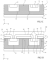
Figures 1A-1D are cross-sections of a semiconductor material wafer, in successive steps of a process for manufacturing a power electronic device, according to a first embodiment of the present solution; -
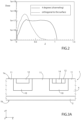
Figure 2 shows plots of doping profiles, which may be implemented in a current spreading layer in the power electronic device; and -
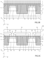
Figures 3A-3C are cross-sections of a semiconductor material wafer, in successive steps of a process for manufacturing a power electronic device, in accordance with a second embodiment of the present solution. - As will be described in detail below, one aspect of the present solution envisages formation of a current spreading layer (CSL layer) in a power electronic device, in particular made of silicon carbide, by a channeled ion implantation process (in a so-called "channeling" condition).
- In a known manner, the channeling condition occurs when the direction of the implanted ion beam is oriented along one of the semiconductor material crystallographic axes, substantially parallel thereto.
- When implanted in the crystal lattice, the ions generally tend to disperse due to impacts with the atoms of the crystal lattice (according to the phenomenon of impact scattering).
- When the implant direction is oriented to an oblique angle with respect to the main axes of the crystal lattice, the atoms in the lattice have a random distribution with respect to the implant direction; the probability of collisions between the implanted ions and the atoms of the crystal lattice is therefore substantially uniform as the depth varies. Therefore, in this implant condition, doping profiles, which are substantially Gaussian with respect to the depth, are obtained, where the depth reached by the implant is determined by the energy, the ions used and the atomic structure of the target.
- If the implant direction is instead a channeling direction, close to a main axis of the crystal lattice, the atoms in the crystal lattice define "channels" that may be traversed by the implanted ions. This reduces the probability of collisions between the implanted ions and the atoms of the crystal lattice, especially near the surface of the wafer wherein the implant occurs, resulting in that the depth of the same implant may be significantly increased.
- In general, the implant channeling occurs when the implant direction is within a critical angle with respect to the channeling direction. In this configuration, the loss of electron energy (interaction with the electron clouds of the crystal atoms) is prevalent with respect to the nuclear loss (impacts with the crystal nuclei). The value of the critical angle depends for example on the direction, the species and the energy used.
- As used herein, the term "implant angle" refers to the tilt angle of the wafer during the implant. It may be defined in general as angle with respect to the surface of the wafer. In general, the surface of the wafer is not a crystallographic plane, as it is defined by a cut angle suitable for subsequent epitaxial processes, for example 4°; in the example, therefore, to identify the <0001> direction of the crystal lattice during the implant, the wafer needs to be tilted with a tilt angle of 4°.
- Channeling is typically an undesired effect during manufacturing of power electronic devices (for example, because the implant depth may be greater than the desired depth and because it is difficult to control the value of the same depth) and the implant direction is therefore generally oriented in a non-channeling direction, to minimize channeling effects.
- As previously indicated, the present Applicant has however realized the possibility of providing, in a controlled and repeatable manner, channeled implants within the process for manufacturing a silicon-carbide power electronic device, in particular for forming a corresponding current spreading layer.
- With reference first to
Figure 1A , a first embodiment of the present solution initially envisages the provision of awafer 1 comprising asubstrate 2 of silicon carbide, for example of 4H-SiC-type having a doping with n-type conductivity (for example with a dose of the order of 5e18 ions cm-3), and delimited by afront surface 1a and arear surface 1b, having a main extension in a horizontal plane xy and opposite to each other along a vertical axis z, orthogonal to the horizontal plane xy. - As shown schematically in the same
Figure 1A , an epitaxial growth is then performed for forming adrift layer 4 on thesubstrate 2, also having a n-type conductivity, for example n- (with a dose of the order of 5e15 ions cm-3); thisdrift layer 4 therefore defines thefront surface 1a of thewafer 1. - In particular, following the epitaxial growth, the silicon carbide crystallographic lattice is oriented at a certain angle (non-zero) with respect to the surface of the
wafer 1. In a possible implementation, the 4H-SiC lattice structure has an off-cut angle of about 4° (intended as the angle between the surface of thewafer 1 and the main crystallographic plane, for example along the <0001> direction). - According to one aspect of the present solution, as shown in
Figure 1B , a blank implant is then performed in the active area in channeling condition for forming a current spreading layer (CSL) 6, continuous and seamless, in proximity of thefront surface 1a of thewafer 1, having n-type conductivity and greater doping than that of the drift layer 4 (thus operating as an enrichment layer). - In particular, the implant is performed at a certain angle (tilt angle) with respect to a direction orthogonal to the
front surface 1a of thewafer 1, in such a way as to provide the channeling conditions and thus allow the channeling of the implanted ions towards the depth of thedrift layer 4. - In the previously discussed implementation (with the 4H-SiC lattice and considering that the implant is performed with phosphorus, P, atoms with an implant energy for example equal to 240 keV), the ion implant may be performed with a tilt angle comprised between 3.5° and 4.5°, for example equal to about 4°, in such a way that the implantation occurs substantially in a channeled manner along the <0001> direction of the crystal lattice.
- The implant dose may be for example of about 8·1012 ions cm-2 (nominal) and the implantation may be performed at room temperature.
-
Figure 2 shows the implant profile (i.e. the implant dose as a function of the depth in thedrift layer 4 along the vertical axis z) in two different conditions: with an implantation performed in channeling condition, in the example with tilt angle equal to 4° (profile shown in solid line); and with an implantation with a direction orthogonal to the surface, with a substantially zero tilt angle (profile shown in dashed line). - It is evident that the channeled implant allows a substantially flat doping profile to be obtained, within a desired depth of the current spreading
layer 6 starting from thefront surface 1a of the wafer 1 (this depth being for example comprised between 0.5 and 5 µm, for example equal to 2 µm). - In greater detail, the present Applicant has experimentally demonstrated that the discussed channeled ion implantation allows a very precise control of the doping of the current spreading
layer 6, in particular with variations lower than 1% with respect to a desired value (in this regard, in case of epitaxial manufacturing of the same current spreading layer, typical doping variations of the order of 10% are obtained). - This allows for improved performances of the resulting power electronic device in terms of on-state resistance (Ron), breakdown voltage (BV) and drain-source leakage current IDSS.
- Furthermore, the aforementioned channeled ion implantation allows very precise control of the depth of the current spreading
layer 6, in particular with variations lower than 1% with respect to a desired value (in this regard, in case of epitaxial manufacturing of the same current spreading layer typical depth variations of the order of 10% are obtained). - This again allows for improved performances of the resulting power electronic device in terms of breakdown voltage (BV) and drain-source leakage current IDSS and also brings benefits in capacitance control.
- With reference to
Figure 1C , the manufacturing process then proceeds with the formation, in the active area, of elementary cells of the power electronic device. -
Body regions 10 are then initially formed within thedrift layer 4 and in particular within the current spreadinglayer 6, that was previously formed, at thefront surface 1a of thewafer 1, by a masked implantation of p-type doping ions (this implantation being performed in a traditional manner, i.e. with a random ion implant, with a substantially zero tilt angle). - The
body regions 10 are separated at a certain distance from each other along a x axis of the horizontal plane xy; in particular, the portions of thedrift layer 4 betweenadjacent body regions 10, at thefront surface 1a, are defined as intercell or JFET regions and are indicated by 11. - Subsequently, as shown in the same
Figure 1C ,respective source regions 12 are formed, again by masked ion implantation, in this case of n-type (for example with nitrogen or phosphorus ions), within each body region 10 (centrally with respect thereto). Thesesource regions 12 have a depth along the vertical axis z smaller than a corresponding depth of thesame body regions 10. - After the implant, the
wafer 1 may be subjected to annealing for activating the doping ions and for reducing the defects in the crystal lattice. - Thus, as shown in the same
Figure 1C ,body contact regions 14 are formed within some of the source regions 12 (centrally with respect thereto) and at thefront surface 1a of thewafer 1. In particular, as shown in the aforementionedFigure 1C , abody contact region 14 may be formed every twosource regions 12. - These
body contact regions 14, which have the purpose of creating an ohmic contact with therespective body regions 10, are formed again by masked ion implant, in this case of p+ type with a high doping dose (for example comprised between 1014 and 5·1015 ions cm-2), and suitable energy (for example comprised between 10 keV and 300 keV). - After a possible annealing step and the removal of the previously used masks, the
wafer 1 is processed in a known manner, forming insulatedgate structures 16 on thefront surface 1a of thewafer 1 and asource metallization region 18. - In particular, these insulated
gate regions 16 are each formed by: agate insulating region 20, for example of oxide, in contact with thefront surface 1a of thewafer 1, above theaforementioned JFET region 11; a gateconductive region 21, directly superimposed on thegate insulating region 20, of a conductive material; and apassivation region 22, covering the gateconductive region 21 and sealing, together with thegate insulating region 20, the gateconductive region 21. - The gate
conductive regions 21 of theinsulated gate structures 16 are electrically connected in parallel, in a manner not shown here, forming a gate terminal of the MOSFET power electronic device. - The
source metallization region 18, for example of metal material and/or metal silicide, forms a source terminal of the MOSFET power electronic device and extends over thefirst surface 1a of the wafer and over the insulatedgate structures 16, in direct electrical contact with thesource regions 12 and thebody contact regions 14. - In a manner not illustrated, a further metallization region may be formed on the
rear surface 1b of thewafer 1, to form a drain terminal of the same power electronic device. - Each elementary cell of the MOSFET power electronic device, which is indicated as a whole in
Figure 1D by 100, is therefore formed by aninsulated gate structure 16 and by the adjacent portions of thebody 10 andsource 12 regions, as well as by theunderlying JFET region 11. - A second embodiment of the present solution is now described, which differs from what has been previously described, due to a different formation of the current spreading layer, which is again denoted by 6, which in this case is not continuous in the active area (as in the first embodiment), but comprises a plurality of distinct portions, which are denoted by 6'.
- In particular, these distinct portions 6' extend only at, and in a localized manner with respect to, the
JFET regions 11 of the elementary cells of the MOSFET power electronic device; the same distinct portions 6' of the current spreadinglayer 6 do not extend in this case in the portions of thedrift layer 4 below the source regions 12 (and the body regions 10) of the elementary cells. - In detail and with reference first to
Figure 3A , the manufacturing process in this case envisages, after formation of the drift layer 4 (as previously discussed), the formation thebody regions 10 in thesame drift layer 4, at thefront surface 1a of thewafer 1. - Then, again as previously discussed, the
source regions 12 are formed within thebody regions 10 and, in the example illustrated, thebody contact regions 14 within some of thesource regions 12. - In this second embodiment, as shown in
Figure 3B , only at this point the ion implantation is carried out in channeling condition (for example, as previously discussed with a tilt of 4° and at room temperature) for the formation of the current spreadinglayer 6, and in particular of the corresponding distinct portions 6' which extend at, and in a localized manner with respect to, theJFET regions 11. - The source regions 12 (and the body contact regions 14) are in fact surface regions heavily damaged from the point of view of the crystal lattice, having been subject to previous doping by ion implantation (performed in a traditional manner, i.e. with a substantially zero tilt angle). The crystal lattice at these heavily damaged regions therefore represents a barrier to the implanted ions, which distribute randomly without penetrating in depth.
- As a result, the ion implantation in channeling condition is performed in a self-aligned manner with respect to these
source regions 12, so that the implanted ions proceed along a depth direction, due to the channeling condition, only at theJFET regions 11, for forming the aforementioned distinct portions 6' of the CSL layer 6 (having, at the end of the implantation, a greater depth than the body regions 10). - Substantially, in the damaged regions, the implantation produces a profile with a very small depth and a substantially negligible random implant peak, such as not to alter (or in any case so as to modify in a limited and controllable manner) doping of the source regions 12 (and, if any, of the body contact regions 14). Conversely, where the same damaged regions (which act as an implant mask) are not present, a flat implant profile is generated in the depth direction in the
drift layer 4, in a manner completely analogous to what has been previously discussed with reference toFigure 2 (with the difference that, in this case, this doping profile is localized to the sole JFET regions 11). - The depth of the ion implantation is therefore modulated in a self-aligned manner with respect to the
aforementioned source regions 12, without resorting to the use of implant masks. - Advantageously, in this second embodiment, the distinct portions 6' of the
CSL layer 6 allow the resistivity of theJFET regions 11 to be reduced in a desired manner, while not varying the characteristics of the portions of thedrift layer 4 underlying thesource regions 12, in particular, without increasing the doping thereof and without varying the characteristics of the body/drain junctions. - The manufacturing process, as shown in
Figure 3C , subsequently proceeds, in a manner similar to what has been previously discussed, by forming theinsulated gate structures 16 on thefront surface 1a of thewafer 1 and thesource metallization region 18 of the resulting powerelectronic device 100. - The advantages of the proposed solution are clear from the previous description.
- In any case, it is underlined that forming the current spreading layer by a single channeled ion implantation step allows the yield to be improved and the costs of the manufacturing process to be reduced (avoiding the repetition of epitaxial growth steps), while improving the electrical characteristics of the resulting power electronic device.
- Furthermore, carrying out the channeled ion implantation in a manner self-aligned to the source regions formed prior to the same implantation allows the desired effect of reducing the resistivity of the JFET regions to be obtained, without however degrading the characteristics of the body/drain junction.
- Finally, it is clear that modifications and variations may be made to what is described and illustrated herein without thereby departing from the scope of the present invention, as defined in the attached claims.
- In particular, it is highlighted that the described solution may also find advantageous application in different power electronic devices, for example in diodes or JFET transistors.
- The channeled ion implantation may be performed with different doping ions, for example with nitrogen atoms (instead of phosphorus atoms). However, using phosphorus has proven to be particularly advantageous due to the resulting flat doping profile of the current spreading layer.
- Furthermore, the semiconductor material wafer may be made of a material other than SiC, such as for example GaN.
Claims (15)
- A process for manufacturing a power electronic device (100), comprising:- forming a semiconductor body (4) of silicon carbide, having a first electrical conductivity (n) and a first doping value and defining a front surface (1a);- forming a Current Spreading Layer, CLS, (6) at a surface portion of said semiconductor body (4) facing the front surface (1a), said current spreading layer (6) having the first electrical conductivity (n) and a second doping value, greater than the first doping value;- forming elementary cells of said power electronic device (100) in an active area of said semiconductor body (4) at said front surface (1a),characterized in that forming the current spreading layer (6) comprises performing a channeled ion implantation, in a channeling condition, for implanting doping ions having said first electrical conductivity (n) within said semiconductor body (4).
- The process according to claim 1, wherein said doping ions are phosphorus atoms.
- The process according to claim 1 or 2, wherein said channeled ion implantation is performed along an implantation direction tilted by a non-zero tilt angle with respect to said front surface (1a).
- The process according to claim 3, wherein said tilt angle is comprised between 3.5° and 4.5°, such that said channeled ion implantation is directed along a main axis of the silicon carbide crystallographic lattice of said semiconductor body (4) and the doping ions penetrate within said semiconductor body (4).
- The process according to any of the preceding claims, wherein said channeled ion implantation has a substantially flat implant profile along a vertical axis (z) orthogonal to said front surface (1a) in a depth direction of said current spreading layer (6).
- The process according to any of the preceding claims, wherein said channeled ion implantation is performed in said active area prior to the step of forming said elementary cells; and wherein said current spreading layer (6) is continuous and seamless in said active area.
- The process according to claim 6, wherein forming said elementary cells comprises:forming first doped regions (12) at said front surface (1a) within said current spreading layer (6), having said first conductivity type (n), separated from each other in a direction (x) parallel to said front surface (1a) by intercell regions (11) of said power electronic device (100);wherein said current spreading layer (6) is configured to locally modulate the resistivity of said intercell regions (11) .
- The process according to any of claims 1-5, wherein forming said elementary cells comprises:forming first doped regions (12) at said front surface (1a), having said first conductivity type (n), separated from each other in a direction (x) parallel to said front surface (1a) by intercell regions (11) of said power electronic device (100);and wherein said channeled ion implantation is performed in a self-aligned manner with respect to said first doped regions (12).
- The process according to claim 8, wherein said first doped regions (12) are damaged regions of the silicon carbide crystallographic lattice, such as to block a propagation of said channeled ion implantation along a vertical axis (z) orthogonal to said front surface (1a) in a depth direction of said semiconductor body (4).
- The process according to claim 9, wherein said channeled ion implantation has an implant profile with small depth and substantially negligible implant peak at said first doped regions (12).
- The process according to any of claims 8-10, wherein said current spreading layer (6) comprises a plurality of distinct portions (6') localized at said intercell regions (11) and configured to locally modulate the resistivity of said intercell regions (11); and wherein said distinct portions (6') of the current spreading layer (6) do not extend into said semiconductor body (4) below said first doped regions (12).
- The process according to any of claims 8-11, comprising forming second doped regions (14) within at least some of said first doped regions (12), having a second electrical conductivity (p), opposite to said first electrical conductivity (n), prior to performing said channeled ion implantation.
- The process according to any of the preceding claims, comprising:providing a wafer (1) comprising a substrate (2);and wherein forming a semiconductor body (4) comprises performing an epitaxial growth above said substrate (2) to form said semiconductor body (4).
- The process according to any of the preceding claims, wherein said semiconductor body (4) is of 4H-SiC polytype with an off-cut angle of 4°.
- The process according to any of the preceding claims, wherein said power electronic device (100) is a MOSFET transistor.
Applications Claiming Priority (1)
| Application Number | Priority Date | Filing Date | Title |
|---|---|---|---|
| IT102023000003897A IT202300003897A1 (en) | 2023-03-03 | 2023-03-03 | MANUFACTURING PROCEDURE OF A POWER ELECTRONIC DEVICE EQUIPPED WITH A CURRENT DIFFUSION LAYER |
Publications (2)
| Publication Number | Publication Date |
|---|---|
| EP4425562A2 true EP4425562A2 (en) | 2024-09-04 |
| EP4425562A3 EP4425562A3 (en) | 2024-10-16 |
Family
ID=86329156
Family Applications (1)
| Application Number | Title | Priority Date | Filing Date |
|---|---|---|---|
| EP24159349.0A Pending EP4425562A3 (en) | 2023-03-03 | 2024-02-23 | Process for manufacturing a power electronic device having a current spreading layer |
Country Status (3)
| Country | Link |
|---|---|
| US (1) | US20240297043A1 (en) |
| EP (1) | EP4425562A3 (en) |
| IT (1) | IT202300003897A1 (en) |
Families Citing this family (2)
| Publication number | Priority date | Publication date | Assignee | Title |
|---|---|---|---|---|
| CN119815884A (en) * | 2024-12-24 | 2025-04-11 | 西安电子科技大学芜湖研究院 | A planar silicon carbide JFET device and a method for preparing the same |
| CN120640741B (en) * | 2025-08-07 | 2025-12-02 | 深圳天狼芯半导体有限公司 | A silicon carbide power device and its fabrication method, chip |
Family Cites Families (2)
| Publication number | Priority date | Publication date | Assignee | Title |
|---|---|---|---|---|
| JP7647239B2 (en) * | 2021-03-30 | 2025-03-18 | 富士電機株式会社 | Semiconductor Device |
| US11804537B2 (en) * | 2021-05-04 | 2023-10-31 | Applied Materials, Inc. | Channeled implants for SiC MOSFET fabrication |
-
2023
- 2023-03-03 IT IT102023000003897A patent/IT202300003897A1/en unknown
-
2024
- 2024-02-21 US US18/583,758 patent/US20240297043A1/en active Pending
- 2024-02-23 EP EP24159349.0A patent/EP4425562A3/en active Pending
Also Published As
| Publication number | Publication date |
|---|---|
| US20240297043A1 (en) | 2024-09-05 |
| EP4425562A3 (en) | 2024-10-16 |
| IT202300003897A1 (en) | 2024-09-03 |
Similar Documents
| Publication | Publication Date | Title |
|---|---|---|
| JP7322126B2 (en) | Superjunction power silicon carbide semiconductor devices formed by ion implantation channeling techniques and related methods | |
| US11837629B2 (en) | Power semiconductor devices having gate trenches and buried edge terminations and related methods | |
| EP3025372B1 (en) | Controlled ion implantation into silicon carbide | |
| US20240297043A1 (en) | Process for manufacturing a power electronic device having a current spreading layer | |
| JP7389543B2 (en) | nitride semiconductor device | |
| EP4425533B1 (en) | Process for manufacturing localized ion implants in silicon-carbide power electronic devices | |
| KR102100863B1 (en) | SiC MOSFET power semiconductor device | |
| US5705406A (en) | Method for producing a semiconductor device having semiconductor layers of SiC by the use of an ion-implantation technique | |
| JP2024125203A (en) | Process for manufacturing a power electronic device having a current spreading layer - Patents.com | |
| CN118588541A (en) | Process for producing power electronic devices having a current spreading layer | |
| CN221928090U (en) | Electronic device | |
| US20240297249A1 (en) | Electronic device with auto aligned csl and edge termination structure, and manufacturing method thereof | |
| CN118588540A (en) | Method for making localized ion implantation in silicon carbide power electronic devices | |
| US20250294801A1 (en) | Power mosfet provided with a variable transparency edge ring formed by a high-depth auto-aligned implant | |
| US20260005024A1 (en) | Method of forming a semiconductor device including a plasma doping process | |
| US20250014902A1 (en) | Method of manufacturing a semiconductor device including ion implantation processes | |
| US11527608B2 (en) | Method for producing a transistor device having a superjunction structure | |
| US20250089283A1 (en) | Semiconductor device manufacturing method and semiconductor device | |
| JP2024125279A (en) | Process for producing localized ion implants in silicon carbide power electronic devices - Patents.com | |
| EP4503137A1 (en) | Manufacturing process for silicon carbide power devices with variable dopant concentration | |
| JP2024125202A (en) | Electronic device having self-aligned CSL and edge termination structures and method of manufacture thereof - Patents.com | |
| US10608099B2 (en) | Methods of manufacturing semiconductor devices with a deep barrier layer | |
| JP2025148282A (en) | Power MOSFET with variable transparency edge ring formed by deep self-aligned implantation | |
| US20220231120A1 (en) | Transistor cell including an implanted expansion region | |
| US10128330B1 (en) | Semiconductor device with a buried junction layer having an interspersed pattern of doped and counter-doped materials |
Legal Events
| Date | Code | Title | Description |
|---|---|---|---|
| PUAI | Public reference made under article 153(3) epc to a published international application that has entered the european phase |
Free format text: ORIGINAL CODE: 0009012 |
|
| STAA | Information on the status of an ep patent application or granted ep patent |
Free format text: STATUS: THE APPLICATION HAS BEEN PUBLISHED |
|
| AK | Designated contracting states |
Kind code of ref document: A2 Designated state(s): AL AT BE BG CH CY CZ DE DK EE ES FI FR GB GR HR HU IE IS IT LI LT LU LV MC ME MK MT NL NO PL PT RO RS SE SI SK SM TR |
|
| PUAL | Search report despatched |
Free format text: ORIGINAL CODE: 0009013 |
|
| AK | Designated contracting states |
Kind code of ref document: A3 Designated state(s): AL AT BE BG CH CY CZ DE DK EE ES FI FR GB GR HR HU IE IS IT LI LT LU LV MC ME MK MT NL NO PL PT RO RS SE SI SK SM TR |
|
| RIC1 | Information provided on ipc code assigned before grant |
Ipc: H01L 21/336 20060101ALI20240906BHEP Ipc: H01L 21/04 20060101ALI20240906BHEP Ipc: H01L 29/78 20060101ALI20240906BHEP Ipc: H01L 29/08 20060101ALI20240906BHEP Ipc: H01L 29/04 20060101AFI20240906BHEP |
|
| STAA | Information on the status of an ep patent application or granted ep patent |
Free format text: STATUS: REQUEST FOR EXAMINATION WAS MADE |
|
| 17P | Request for examination filed |
Effective date: 20250415 |