EP4425252A1 - Display module and electronic device - Google Patents
Display module and electronic device Download PDFInfo
- Publication number
- EP4425252A1 EP4425252A1 EP22885800.7A EP22885800A EP4425252A1 EP 4425252 A1 EP4425252 A1 EP 4425252A1 EP 22885800 A EP22885800 A EP 22885800A EP 4425252 A1 EP4425252 A1 EP 4425252A1
- Authority
- EP
- European Patent Office
- Prior art keywords
- layer
- electrode
- display module
- cover plate
- voltage
- Prior art date
- Legal status (The legal status is an assumption and is not a legal conclusion. Google has not performed a legal analysis and makes no representation as to the accuracy of the status listed.)
- Pending
Links
Images


Classifications
-
- G—PHYSICS
- G02—OPTICS
- G02F—OPTICAL DEVICES OR ARRANGEMENTS FOR THE CONTROL OF LIGHT BY MODIFICATION OF THE OPTICAL PROPERTIES OF THE MEDIA OF THE ELEMENTS INVOLVED THEREIN; NON-LINEAR OPTICS; FREQUENCY-CHANGING OF LIGHT; OPTICAL LOGIC ELEMENTS; OPTICAL ANALOGUE/DIGITAL CONVERTERS
- G02F1/00—Devices or arrangements for the control of the intensity, colour, phase, polarisation or direction of light arriving from an independent light source, e.g. switching, gating or modulating; Non-linear optics
- G02F1/01—Devices or arrangements for the control of the intensity, colour, phase, polarisation or direction of light arriving from an independent light source, e.g. switching, gating or modulating; Non-linear optics for the control of the intensity, phase, polarisation or colour
- G02F1/165—Devices or arrangements for the control of the intensity, colour, phase, polarisation or direction of light arriving from an independent light source, e.g. switching, gating or modulating; Non-linear optics for the control of the intensity, phase, polarisation or colour based on translational movement of particles in a fluid under the influence of an applied field
- G02F1/166—Devices or arrangements for the control of the intensity, colour, phase, polarisation or direction of light arriving from an independent light source, e.g. switching, gating or modulating; Non-linear optics for the control of the intensity, phase, polarisation or colour based on translational movement of particles in a fluid under the influence of an applied field characterised by the electro-optical or magneto-optical effect
- G02F1/167—Devices or arrangements for the control of the intensity, colour, phase, polarisation or direction of light arriving from an independent light source, e.g. switching, gating or modulating; Non-linear optics for the control of the intensity, phase, polarisation or colour based on translational movement of particles in a fluid under the influence of an applied field characterised by the electro-optical or magneto-optical effect by electrophoresis
-
- G—PHYSICS
- G02—OPTICS
- G02F—OPTICAL DEVICES OR ARRANGEMENTS FOR THE CONTROL OF LIGHT BY MODIFICATION OF THE OPTICAL PROPERTIES OF THE MEDIA OF THE ELEMENTS INVOLVED THEREIN; NON-LINEAR OPTICS; FREQUENCY-CHANGING OF LIGHT; OPTICAL LOGIC ELEMENTS; OPTICAL ANALOGUE/DIGITAL CONVERTERS
- G02F1/00—Devices or arrangements for the control of the intensity, colour, phase, polarisation or direction of light arriving from an independent light source, e.g. switching, gating or modulating; Non-linear optics
- G02F1/01—Devices or arrangements for the control of the intensity, colour, phase, polarisation or direction of light arriving from an independent light source, e.g. switching, gating or modulating; Non-linear optics for the control of the intensity, phase, polarisation or colour
- G02F1/165—Devices or arrangements for the control of the intensity, colour, phase, polarisation or direction of light arriving from an independent light source, e.g. switching, gating or modulating; Non-linear optics for the control of the intensity, phase, polarisation or colour based on translational movement of particles in a fluid under the influence of an applied field
- G02F1/1675—Constructional details
-
- G—PHYSICS
- G02—OPTICS
- G02F—OPTICAL DEVICES OR ARRANGEMENTS FOR THE CONTROL OF LIGHT BY MODIFICATION OF THE OPTICAL PROPERTIES OF THE MEDIA OF THE ELEMENTS INVOLVED THEREIN; NON-LINEAR OPTICS; FREQUENCY-CHANGING OF LIGHT; OPTICAL LOGIC ELEMENTS; OPTICAL ANALOGUE/DIGITAL CONVERTERS
- G02F1/00—Devices or arrangements for the control of the intensity, colour, phase, polarisation or direction of light arriving from an independent light source, e.g. switching, gating or modulating; Non-linear optics
- G02F1/01—Devices or arrangements for the control of the intensity, colour, phase, polarisation or direction of light arriving from an independent light source, e.g. switching, gating or modulating; Non-linear optics for the control of the intensity, phase, polarisation or colour
- G02F1/165—Devices or arrangements for the control of the intensity, colour, phase, polarisation or direction of light arriving from an independent light source, e.g. switching, gating or modulating; Non-linear optics for the control of the intensity, phase, polarisation or colour based on translational movement of particles in a fluid under the influence of an applied field
- G02F1/1675—Constructional details
- G02F1/16757—Microcapsules
-
- G—PHYSICS
- G02—OPTICS
- G02F—OPTICAL DEVICES OR ARRANGEMENTS FOR THE CONTROL OF LIGHT BY MODIFICATION OF THE OPTICAL PROPERTIES OF THE MEDIA OF THE ELEMENTS INVOLVED THEREIN; NON-LINEAR OPTICS; FREQUENCY-CHANGING OF LIGHT; OPTICAL LOGIC ELEMENTS; OPTICAL ANALOGUE/DIGITAL CONVERTERS
- G02F1/00—Devices or arrangements for the control of the intensity, colour, phase, polarisation or direction of light arriving from an independent light source, e.g. switching, gating or modulating; Non-linear optics
- G02F1/01—Devices or arrangements for the control of the intensity, colour, phase, polarisation or direction of light arriving from an independent light source, e.g. switching, gating or modulating; Non-linear optics for the control of the intensity, phase, polarisation or colour
- G02F1/165—Devices or arrangements for the control of the intensity, colour, phase, polarisation or direction of light arriving from an independent light source, e.g. switching, gating or modulating; Non-linear optics for the control of the intensity, phase, polarisation or colour based on translational movement of particles in a fluid under the influence of an applied field
- G02F1/1675—Constructional details
- G02F1/1676—Electrodes
-
- G—PHYSICS
- G02—OPTICS
- G02F—OPTICAL DEVICES OR ARRANGEMENTS FOR THE CONTROL OF LIGHT BY MODIFICATION OF THE OPTICAL PROPERTIES OF THE MEDIA OF THE ELEMENTS INVOLVED THEREIN; NON-LINEAR OPTICS; FREQUENCY-CHANGING OF LIGHT; OPTICAL LOGIC ELEMENTS; OPTICAL ANALOGUE/DIGITAL CONVERTERS
- G02F1/00—Devices or arrangements for the control of the intensity, colour, phase, polarisation or direction of light arriving from an independent light source, e.g. switching, gating or modulating; Non-linear optics
- G02F1/01—Devices or arrangements for the control of the intensity, colour, phase, polarisation or direction of light arriving from an independent light source, e.g. switching, gating or modulating; Non-linear optics for the control of the intensity, phase, polarisation or colour
- G02F1/165—Devices or arrangements for the control of the intensity, colour, phase, polarisation or direction of light arriving from an independent light source, e.g. switching, gating or modulating; Non-linear optics for the control of the intensity, phase, polarisation or colour based on translational movement of particles in a fluid under the influence of an applied field
- G02F1/1685—Operation of cells; Circuit arrangements affecting the entire cell
-
- G—PHYSICS
- G02—OPTICS
- G02F—OPTICAL DEVICES OR ARRANGEMENTS FOR THE CONTROL OF LIGHT BY MODIFICATION OF THE OPTICAL PROPERTIES OF THE MEDIA OF THE ELEMENTS INVOLVED THEREIN; NON-LINEAR OPTICS; FREQUENCY-CHANGING OF LIGHT; OPTICAL LOGIC ELEMENTS; OPTICAL ANALOGUE/DIGITAL CONVERTERS
- G02F1/00—Devices or arrangements for the control of the intensity, colour, phase, polarisation or direction of light arriving from an independent light source, e.g. switching, gating or modulating; Non-linear optics
- G02F1/01—Devices or arrangements for the control of the intensity, colour, phase, polarisation or direction of light arriving from an independent light source, e.g. switching, gating or modulating; Non-linear optics for the control of the intensity, phase, polarisation or colour
- G02F1/165—Devices or arrangements for the control of the intensity, colour, phase, polarisation or direction of light arriving from an independent light source, e.g. switching, gating or modulating; Non-linear optics for the control of the intensity, phase, polarisation or colour based on translational movement of particles in a fluid under the influence of an applied field
- G02F1/1675—Constructional details
- G02F2001/1678—Constructional details characterised by the composition or particle type
Definitions
- the present disclosure relates to the technical field of electronic devices, and in particular, to a display module and an electronic device.
- OLED organic light-emitting diode
- display screens may have monotonous display modes, and it is difficult for them to adapt to changed scenes. Consequently, user experience is degraded.
- the purpose of embodiments of the present disclosure is to provide a display module and an electronic device, to solve a problem that user experience is degraded due to a monotonous display mode of a display screen.
- the present disclosure is implemented as follows.
- an embodiment of the present disclosure provides a display module including a composite light-emitting layer, an electronic ink layer, and a cover plate layer disposed in sequence.
- the electronic ink layer includes a plurality of capsule bodies, and the plurality of capsule bodies are arranged along a plane on which the cover plate layer is located, where a first electrode and a second electrode are provided on a periphery of the capsule body, the first electrode is a transparent electrode and is disposed parallel to the cover plate layer, and the second electrode is disposed perpendicular to the cover plate layer; and ink particles are accommodated in the capsule body.
- the ink particles are distributed along the first electrode and the display module performs displaying through the electronic ink layer; and in a case that a voltage is applied to the second electrode and a voltage is applied to the composite light-emitting layer, the ink particles are distributed along the second electrode and the display module performs displaying through the composite light-emitting layer.
- an embodiment of the present disclosure provides an electronic device, including the foregoing display module.
- the composite light-emitting layer, the electronic ink layer, and the cover plate layer are disposed in sequence on the display module.
- the electronic ink layer includes the plurality of capsule bodies, and the plurality of capsule bodies are arranged along the plane on which the cover plate layer is located, where the first electrode and the second electrode are provided on the periphery of the capsule body, the first electrode is a transparent electrode and is disposed parallel to the cover plate layer, and the second electrode is disposed perpendicular to the cover plate layer; and the ink particles are accommodated in the capsule body.
- the ink particles are distributed along the first electrode and the display module performs displaying through the electronic ink layer; and in the case that a voltage is applied to the second electrode and a voltage is applied to the composite light-emitting layer, the ink particles are distributed along the second electrode and the display module performs displaying through the composite light-emitting layer.
- the display module can switch the display mode according to the user's needs, improving the user's experience.
- first”, “second”, and the like are intended to distinguish between similar objects but do not indicate a specific order or sequence. It should be understood that data used in this way is used interchangeably in appropriate circumstances so that the embodiments of the present disclosure can be implemented in other orders than the order illustrated or described herein.
- first”, “second”, and the like are usually used to distinguish objects of a same type, and do not restrict a quantity of objects. For example, there may be one or a plurality of first objects.
- “and/or” in the specification and claims represents at least one of connected objects, and the character “/" generally indicates that the contextually associated objects have an "or” relationship.
- the present disclosure discloses a display module including a composite light-emitting layer, an electronic ink layer, and a cover plate layer 100 stacked sequentially along a main light-emitting direction.
- the display module of the present disclosure has the following features:
- the display module can choose to emit light through the composite light-emitting layer or the electronic ink layer according to different application scenarios and user needs, so as to switch a display mode of the display module, thereby improving user experience. Detailed descriptions are provided below.
- the cover plate layer 100 in the present disclosure is a light-emitting side of the display module, and is a side that the display module faces the user, and the cover plate layer 100 is conventionally a glass cover plate to ensure good light transmittance and to protect internal devices of the display module.
- the electronic ink layer includes a plurality of capsule bodies 200.
- the plurality of capsule bodies 200 are arranged along a plane on which the cover plate layer 100 is located.
- the plurality of capsule bodies 200 are arranged in an array distribution to form the electronic ink layer.
- the plurality of capsule bodies 200 are arranged in a direction perpendicular to the main light-emitting direction of the display module.
- a first electrode 210 and a second electrode 220 are provided on a periphery of the capsule body 200.
- the first electrode 210 is a transparent electrode and is disposed parallel to the cover plate layer 100
- the second electrode 220 is disposed perpendicular to the cover plate layer 100, so as to generate electric field forces in different directions, thereby changing a distribution direction of ink particles 201.
- the ink particles 201 are accommodated in the capsule body 200.
- the ink particles 201 may include a plurality of first color particles and a plurality of second color particles.
- first color particles and the second color particles one type is black particles and the other type is white particles, and the first color particles and the second color particles have opposite electrical properties.
- the display module in the present disclosure may be controlled in the following manners: In a case that a voltage is applied to the first electrode 210, an electric field is created between a cathode and an anode of the first electrode 210, and an electrophoretic phenomenon occurs under the action of the electric field to realize distribution of the ink particles 201 along the first electrode 210. Specifically, among the plurality of black particles and the plurality of white particles, one type moves toward the cathode of the first electrode 210 and the other type moves toward the anode of the first electrode 210. For example, the black particles move toward the cathode of the first electrode 210, and the white particles move toward the anode of the first electrode 210.
- the display module is in a first display state shown in FIG. 7 .
- the display module performs displaying through the electronic ink layer, and specifically at this time a display screen is in a black and white display mode.
- the display module is in a second display state shown in FIG. 8 , the composite light-emitting layer can emit light to the cover plate layer 100 through the second light transmission gap, and the display module can perform displaying through the composite light-emitting layer.
- the composite light-emitting layer can be an OLED light-emitting layer, and the OLED light-emitting layer has a fast refresh speed so that the display module can be switched to the second display state for use when a user has a need for applications such as movie watching and gaming.
- the electronic ink layer implements position shifting of the black particles and the white particles within the capsule body 200 according to a change in a direction of the voltage loaded between the cathode and the anode of the first electrode 210, thereby implementing screen refreshment.
- the electronic ink layer has low power consumption, and ensures more comfort and better eye protection with a display effect close to that of paper. In this way, when a user has such needs as long-time reading, the user can switch the display module to the first display state for use.
- the user can switch display states of the display module according to different application scenarios and different needs, so that the display module has better versatility and improved user experience.
- the first electrode 210 being made of a transparent electrode is to ensure good light transmittance, thereby avoiding interference with light emitted from the composite light-emitting layer.
- the electronic ink layer may employ an arrangement as shown in FIG. 1 and FIG. 2 .
- the second electrode 220 may include a plurality of second cathodes and second anodes arranged alternately parallel to the cover plate layer 100, where the capsule body 200 is provided between the second cathode and the second anode that are adjacent.
- adjacent capsule bodies 200 can both use the second cathode or second anode located between the two of them. This can reduce the number of second cathodes and the number of second anodes required, reducing material costs.
- the electronic ink layer may alternatively employ an arrangement in FIG. 3 and FIG. 4 .
- the capsule body 200 may further be provided with a third electrode 230 on the periphery of the capsule body.
- a disposing direction of the third electrode 230 intersects with the cover plate layer 100.
- the disposing direction of the third electrode 230 coincides with a disposing direction of the second electrode 220, and the third electrode 230 is disposed between the second electrode 220 and the cover plate layer 100.
- the third electrode 230 in the case that a voltage is applied to the third electrode 230, among the black particles and the white particles in the ink particles 201, one type moves toward a cathode of the third electrode 230, and the other type moves toward an anode of the third electrode 230, so that the plurality of black particles and the plurality of white particles are disposed sequentially in a direction parallel to the cover plate layer 100, to distribute the ink particles 201 along the third electrode 230 to form a third light transmission gap.
- the third light transmission gap is smaller than the second light transmission gap.
- the third light transmission gap is smaller than the second light transmission gap, light coming from the sides is blocked by the black particles and the white particles in the ink particles 201, and the user can see, from only one direction, for example, a direction directly facing the display module, an image displayed by the display module. In this way, when the user is using the display module, other people cannot pry into the image displayed by the display module. This is beneficial to the user's privacy protection, and enriches display modes of the display module, further improving user experience.
- the third electrode 230 can also be disposed in accordance with the second electrode 220.
- the third electrode 230 may include a plurality of third cathodes and third anodes arranged alternately parallel to the cover plate layer 100.
- the capsule body 200 is provided between the third cathode and the third anode that are adjacent, thereby implementing reuse of the third cathodes and the third anodes, thereby saving material costs.
- the capsule body 200 is further provided with a fourth electrode 240 on the periphery of the capsule body.
- a disposing direction of the fourth electrode 240 intersects with the cover plate layer 100, and the fourth electrode 240 is disposed between the second electrode 220 and the composite light-emitting layer.
- a voltage is applied to the fourth electrode 240, an electric field force action is created between a cathode and an anode of the fourth electrode 240.
- the ink particles 201 are distributed along the fourth electrode 240 to form a fourth light transmission gap.
- the fourth light transmission gap is smaller than the second light transmission gap. Therefore, in the case that a voltage is applied to the fourth electrode 240 and a voltage is applied to the composite light-emitting layer, light emitted from the composite light-emitting layer is irradiated to the cover plate layer 100 through the fourth light transmission gap, so that the display module can be in the third display state shown in FIG. 9 .
- the fourth electrode 240 may be understood as a spare part of the third electrode 230, and the fourth electrode 240 implements a function similar to that of the third electrode 230, both of which are to implement privacy protection for the user.
- the fourth electrode 240 may be understood as a mirror structure of the third electrode 230 that is symmetric to the third electrode 230 about the capsule body 200, thereby forming the foregoing fourth light transmission gap.
- the fourth electrode 240 can also be disposed in accordance with the second electrode 220.
- the fourth electrode 240 includes a plurality of fourth cathodes and fourth anodes arranged alternately parallel to the cover plate layer 100.
- the capsule body 200 is provided between the fourth cathode and the fourth anode that are adjacent, to implement reuse of the fourth cathode and the fourth anode, thereby saving material costs.
- the electronic ink layer may alternatively employ an arrangement in FIG. 5 and FIG. 6 .
- a plurality of second electrodes 220, a plurality of third electrodes 230, and a plurality of fourth electrodes 240 may be provided.
- the plurality of second electrodes 220, the plurality of third electrodes 230, and the plurality of fourth electrodes 240 may all be arranged parallel to the cover plate layer 100.
- the second electrodes 220, the third electrodes 230, and the fourth electrodes 240 are all electrode pairs, and they all correspond to the capsule bodies 200, respectively, to form a plurality of capsule body components, so that the capsule bodies 200 can be better independently manipulated.
- the capsule body 200 may be set to have a shape as formed by two mutually mirrored circular truncated cone or cones, and a desired light transmission gap may be formed by constraining the shape of the capsule body 200.
- the capsule body 200 is designed as a sphere in the present disclosure.
- a chord length corresponding to the capsule body 200 at any height position in a height range in which the second electrode 220 is located is greater than a chord length corresponding to the capsule body 200 at any height position in a height range in which the third electrode 230 is located, and is greater than a chord length corresponding to the capsule body 200 at any height position in a height range in which the fourth electrode 240 is located.
- a direction of the height coincides with a direction in which the composite light-emitting layer, the electronic ink layer, and the cover plate layer 100 are disposed in sequence, and a direction of the chord length is perpendicular to the direction of the height.
- the ink particles 201 are distributed along the second electrode 220, and a spacing between the plurality of black particles and the plurality of white particles in the ink particles 201, that is, the second light transmission gap, has a maximum value.
- the electronic ink layer can have better light transmittance, thereby ensuring a display effect of the display module in the second display state shown in FIG. 8 .
- the formed third light transmission gap or fourth light transmission gap is smaller than the second light transmission gap. This ensures a constraint on a direction of light emitted by the composite light-emitting layer, and guarantees a display effect of the display module in the third display state shown in FIG. 9 , implementing privacy protection.
- a vertical bisector of the first electrode 210, a vertical bisector of the second electrode 220, a vertical bisector of the third electrode 230, and a vertical bisector of the fourth electrode 240 all pass through a center of sphere of the capsule body 200.
- a larger electric field force can be generated, acting on the ink particles 201 so that a layout direction of the ink particles 201 can be more effectively adjusted according to a position of the applied voltage. This is more conducive to the formation of the second light transmission gap, the third light transmission gap, and the fourth light transmission gap.
- the first electrode 210, the second electrode 220, the third electrode 230, and the fourth electrode 240 may be combined to form an octagonal shape, to surround the capsule body 200.
- the first electrode 210, the second electrode 220, the third electrode 230, and the fourth electrode 240 are all provided as electrode plates.
- the first cathode and the first anode are both disposed parallel to the cover plate layer 100, and the second cathode and the second anode are both disposed perpendicular to the cover plate layer 100.
- the third cathode and the third anode are arranged at an angle to each other, such as 135°, and are both disposed between the second electrode 220 and the first cathode.
- the fourth cathode and the fourth anode are arranged at an angle to each other, such as 135°, and are both disposed between the second electrode 220 and the first anode.
- Such a setting makes the layout structure more compact, improving a space utilization rate. It should be noted herein that the foregoing angle may alternatively be 90° or the like. Details are not described herein.
- a first light transmission gap may be present between adjacent capsule bodies 200, and the second electrode 220, the third electrode 230, and the fourth electrode 240 may all be disposed in the first light transmission gap.
- the display module performs displaying through the electronic ink layer and the composite light-emitting layer, thereby creating a fourth display state shown in FIG. 10 .
- the electronic ink layer emits light, which is irradiated to the cover plate layer 100, and light emitted from the composite light-emitting layer is also irradiated to the cover plate layer 100 through the first light transmission gap.
- the display module will have a display effect of a color ink screen. This can enrich display modes of the display module, further improving user experience.
- the first electrode 210, the second electrode 220, the third electrode 230, and the fourth electrode 240 can all be fabricated by selecting a transparent polar plate to ensure a good conductive effect and light transmittance.
- the transparent designs of the second electrode 220, the third electrode 230, and the fourth electrode 240 can avoid interference with the light emitted from the composite light-emitting layer, further guaranteeing the display effect.
- the composite light-emitting layer and the electronic ink layer of the display module may employ a layout in FIG. 5 and FIG. 6 .
- a plurality of first electrodes 210 may be provided, the plurality of first electrodes 210 are arranged parallel to the cover plate layer 100.
- the first electrodes 210 are corresponding to the capsule bodies 200, respectively, meaning a one-to-one control mode is implemented between the first electrodes 210 and the capsule bodies 200.
- the composite light-emitting layer may include a fifth cathode layer 800, an electron transport layer 700, an organic light-emitting layer 600, a hole transport layer 500, and a fifth anode layer 400 stacked sequentially.
- the fifth anode layer 400 is a transparent anode layer and is provided on a side of the composite light-emitting layer facing the electronic ink layer, ensuring light transmittance and avoiding interference with the light emitted from the composite light-emitting layer.
- the fifth cathode layer 800 and the fifth anode layer 400 are energized, electrons are transmitted from the fifth cathode layer 800 to the electron transport layer 700, and electron holes are injected from the fifth anode layer 400 into the hole transport layer 500. Then, the electrons and the electron holes migrate to the organic light-emitting layer 600, and excitons are generated after the electrons and the electron holes meet, implementing light emission of the composite light-emitting layer.
- the fifth anode layer 400 may be made of ITO material, and the ITO material is typically referred to as indium tin oxide, which is an N-type oxide semiconductor.
- the fifth anode layer 400 is typically fabricated as an ITO thin film structure, that is, an indium tin oxide semiconductor transparent conductive film, to ensure good resistivity and light transmittance. Therefore, the fifth anode layer 400 in the composite light-emitting layer is located on the side toward the electronic ink layer, implementing effective light emission.
- the fifth cathode layer 800 may be fabricated by using a metal electrode, such as magnesium or lithium. Details are not described herein.
- a transparent insulating layer 300 may further be provided between the composite light-emitting layer and the electronic ink layer, and the transparent insulating layer 300 can prevent short circuit between the composite light-emitting layer and the electronic ink layer, thereby ensuring effective displaying of the display module in each display state.
- a transparent resin may be used to ensure good light transmittance and insulating properties, preventing interference with irradiation of light emitted from the composite light-emitting layer to the cover plate layer 100.
- the composite light-emitting layer and the electronic ink layer of the display module may alternatively employ a layout in FIG. 11 and FIG. 12 .
- the first electrode 210 may include a first cathode layer 211 and a first anode layer 212 spaced apart, the first cathode layer 211 and the first anode layer 212 are both disposed parallel to the cover plate layer 100, and the plurality of capsule bodies 200 are all disposed between the first cathode layer 211 and the first anode layer 212.
- the composite light-emitting layer includes a fifth cathode layer 800, an electron transport layer 700, an organic light-emitting layer 600, and a hole transport layer 500 stacked sequentially toward the electronic ink layer, and the first anode layer 212 is located between the hole transport layer 500 and the plurality of capsule bodies 200.
- the display module performs displaying through the electronic ink layer.
- the display module performs displaying through the composite light-emitting layer.
- the composite light-emitting layer and the electronic ink layer both use the first anode layer 212, and the composite light-emitting layer does not need to be additionally provided with a fifth anode layer 400 as in the layout solution shown in FIG. 5 and FIG. 6 . This can reduce material costs and is conducive to overall thinning of the display module.
- Embodiments of the present disclosure further disclose an electronic device.
- the electronic device includes the display module in any one of the foregoing embodiments.
- the electronic device disclosed in embodiments of the present disclosure may be a smartphone, a tablet computer, an e-book reader, a wearable device (for example, a smart watch), a game console, or other devices.
- a specific type of the electronic device is not limited in embodiments of the present disclosure.
Landscapes
- Physics & Mathematics (AREA)
- Nonlinear Science (AREA)
- General Physics & Mathematics (AREA)
- Optics & Photonics (AREA)
- Health & Medical Sciences (AREA)
- Life Sciences & Earth Sciences (AREA)
- Chemical & Material Sciences (AREA)
- Chemical Kinetics & Catalysis (AREA)
- Electrochemistry (AREA)
- Molecular Biology (AREA)
- Electroluminescent Light Sources (AREA)
- Devices For Indicating Variable Information By Combining Individual Elements (AREA)
Abstract
Description
- This application claims priority to
Chinese Patent Application No. 202111248982.2, filed on October 26, 2021 - The present disclosure relates to the technical field of electronic devices, and in particular, to a display module and an electronic device.
- Nowadays, electronic displays are available in various display modes, which can meet people's visual needs such as watching movies, playing games and reading. There are, for example, organic light-emitting diode (OLED) displays and electronicink displays.
- However, regardless of the type of electronic display, due to different lighting mechanisms thereof, display screens may have monotonous display modes, and it is difficult for them to adapt to changed scenes. Consequently, user experience is degraded.
- The purpose of embodiments of the present disclosure is to provide a display module and an electronic device, to solve a problem that user experience is degraded due to a monotonous display mode of a display screen.
- To solve the foregoing technical problem, the present disclosure is implemented as follows.
- According to a first aspect, an embodiment of the present disclosure provides a display module including a composite light-emitting layer, an electronic ink layer, and a cover plate layer disposed in sequence. The electronic ink layer includes a plurality of capsule bodies, and the plurality of capsule bodies are arranged along a plane on which the cover plate layer is located, where a first electrode and a second electrode are provided on a periphery of the capsule body, the first electrode is a transparent electrode and is disposed parallel to the cover plate layer, and the second electrode is disposed perpendicular to the cover plate layer; and ink particles are accommodated in the capsule body. In a case that a voltage is applied to the first electrode, the ink particles are distributed along the first electrode and the display module performs displaying through the electronic ink layer; and in a case that a voltage is applied to the second electrode and a voltage is applied to the composite light-emitting layer, the ink particles are distributed along the second electrode and the display module performs displaying through the composite light-emitting layer.
- According to a second aspect, an embodiment of the present disclosure provides an electronic device, including the foregoing display module.
- Beneficial effects of the present disclosure are as follows:
In the present disclosure, the composite light-emitting layer, the electronic ink layer, and the cover plate layer are disposed in sequence on the display module. The electronic ink layer includes the plurality of capsule bodies, and the plurality of capsule bodies are arranged along the plane on which the cover plate layer is located, where the first electrode and the second electrode are provided on the periphery of the capsule body, the first electrode is a transparent electrode and is disposed parallel to the cover plate layer, and the second electrode is disposed perpendicular to the cover plate layer; and the ink particles are accommodated in the capsule body. - In this way, in the case that a voltage is applied to the first electrode, the ink particles are distributed along the first electrode and the display module performs displaying through the electronic ink layer; and in the case that a voltage is applied to the second electrode and a voltage is applied to the composite light-emitting layer, the ink particles are distributed along the second electrode and the display module performs displaying through the composite light-emitting layer.
- In conclusion, through such structural settings and operation mode, the display module can switch the display mode according to the user's needs, improving the user's experience.
-
-
FIG. 1 is a structural diagram of a display module disclosed in a first embodiment of the present disclosure; -
FIG. 2 is a structural diagram of an electronic ink layer disclosed in the first embodiment of the present disclosure; -
FIG. 3 is a structural diagram of a display module disclosed in a second embodiment of the present disclosure; -
FIG. 4 is a structural diagram of an electronic ink layer disclosed in the second embodiment of the present disclosure; -
FIG. 5 is a structural diagram of a display module disclosed in a third embodiment of the present disclosure; -
FIG. 6 is a structural diagram of an electronic ink layer disclosed in the third embodiment of the present disclosure; -
FIG. 7 is a diagram of a second display state of the display module disclosed in the third embodiment of the present disclosure; -
FIG. 8 is a diagram of a first display state of the display module disclosed in the third embodiment of the present disclosure; -
FIG. 9 is a diagram of a third display state of the display module disclosed in the third embodiment of the present disclosure; -
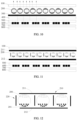
FIG. 10 is a diagram of a fourth display state of the display module disclosed in the third embodiment of the present disclosure; -
FIG. 11 is a structural diagram of a display module disclosed in a fourth embodiment of the present disclosure; and -
FIG. 12 is a structural diagram of an electronic ink layer disclosed in the fourth embodiment of the present disclosure. -
- 100-cover plate layer;
- 200-capsule body, 201-ink particle;
- 210-first electrode, 211-first cathode layer, 212-first anode layer;
- 220-second electrode, 230-third electrode, 240-fourth electrode;
- 300-transparent insulating layer;
- 800-fifth cathode layer, 700-electron transport layer, 600-organic light-emitting layer, 500-hole transport layer, 400-fifth anode layer.
- The following clearly describes the technical solutions in embodiments of the present disclosure with reference to the accompanying drawings in embodiments of the present disclosure. It is clear that the described embodiments are some but not all of the embodiments of the present disclosure. Based on the embodiments in the present disclosure, all other embodiments obtained by persons of ordinary skill in the art without creative efforts fall within the protection scope of the present disclosure.
- In the specification and claims of the present disclosure, terms "first", "second", and the like are intended to distinguish between similar objects but do not indicate a specific order or sequence. It should be understood that data used in this way is used interchangeably in appropriate circumstances so that the embodiments of the present disclosure can be implemented in other orders than the order illustrated or described herein. In addition, "first", "second", and the like are usually used to distinguish objects of a same type, and do not restrict a quantity of objects. For example, there may be one or a plurality of first objects. In addition, "and/or" in the specification and claims represents at least one of connected objects, and the character "/" generally indicates that the contextually associated objects have an "or" relationship.
- A display module and an electronic device provided in embodiments of the present disclosure are described in detail below by using specific embodiments and application scenarios thereof in combination with the accompanying drawings.
- Refer to
FIG. 1 to FIG. 12 . The present disclosure discloses a display module including a composite light-emitting layer, an electronic ink layer, and acover plate layer 100 stacked sequentially along a main light-emitting direction. The display module of the present disclosure has the following features: The display module can choose to emit light through the composite light-emitting layer or the electronic ink layer according to different application scenarios and user needs, so as to switch a display mode of the display module, thereby improving user experience. Detailed descriptions are provided below. - The
cover plate layer 100 in the present disclosure is a light-emitting side of the display module, and is a side that the display module faces the user, and thecover plate layer 100 is conventionally a glass cover plate to ensure good light transmittance and to protect internal devices of the display module. - The electronic ink layer includes a plurality of
capsule bodies 200. The plurality ofcapsule bodies 200 are arranged along a plane on which thecover plate layer 100 is located. For example, the plurality ofcapsule bodies 200 are arranged in an array distribution to form the electronic ink layer. The plurality ofcapsule bodies 200 are arranged in a direction perpendicular to the main light-emitting direction of the display module. - A
first electrode 210 and asecond electrode 220 are provided on a periphery of thecapsule body 200. Thefirst electrode 210 is a transparent electrode and is disposed parallel to thecover plate layer 100, and thesecond electrode 220 is disposed perpendicular to thecover plate layer 100, so as to generate electric field forces in different directions, thereby changing a distribution direction ofink particles 201. - The
ink particles 201 are accommodated in thecapsule body 200. Theink particles 201 may include a plurality of first color particles and a plurality of second color particles. Among the first color particles and the second color particles, one type is black particles and the other type is white particles, and the first color particles and the second color particles have opposite electrical properties. - The display module in the present disclosure may be controlled in the following manners:
In a case that a voltage is applied to thefirst electrode 210, an electric field is created between a cathode and an anode of thefirst electrode 210, and an electrophoretic phenomenon occurs under the action of the electric field to realize distribution of theink particles 201 along thefirst electrode 210. Specifically, among the plurality of black particles and the plurality of white particles, one type moves toward the cathode of thefirst electrode 210 and the other type moves toward the anode of thefirst electrode 210. For example, the black particles move toward the cathode of thefirst electrode 210, and the white particles move toward the anode of thefirst electrode 210. In this way, the plurality of black particles and the plurality of white particles are sequentially disposed along the main light-emitting direction of the display module. In this case, the display module is in a first display state shown inFIG. 7 . The display module performs displaying through the electronic ink layer, and specifically at this time a display screen is in a black and white display mode. - In a case that a voltage is applied to the
second electrode 220 and a voltage is applied to the composite light-emitting layer, an electric field is formed between a cathode and an anode of thesecond electrode 220, and an electrophoretic phenomenon occurs under the action of the electric field, to realize distribution of theink particles 201 along thesecond electrode 220. Specifically, the plurality of black particles and the plurality of white particles are sequentially disposed in a direction parallel to thecover plate layer 100, and a second light transmission gap is formed between the plurality of black particles and the plurality of white particles. In this case, the display module is in a second display state shown inFIG. 8 , the composite light-emitting layer can emit light to thecover plate layer 100 through the second light transmission gap, and the display module can perform displaying through the composite light-emitting layer. - In the foregoing settings, the composite light-emitting layer can be an OLED light-emitting layer, and the OLED light-emitting layer has a fast refresh speed so that the display module can be switched to the second display state for use when a user has a need for applications such as movie watching and gaming.
- The electronic ink layer implements position shifting of the black particles and the white particles within the
capsule body 200 according to a change in a direction of the voltage loaded between the cathode and the anode of thefirst electrode 210, thereby implementing screen refreshment. The electronic ink layer has low power consumption, and ensures more comfort and better eye protection with a display effect close to that of paper. In this way, when a user has such needs as long-time reading, the user can switch the display module to the first display state for use. - In conclusion, the user can switch display states of the display module according to different application scenarios and different needs, so that the display module has better versatility and improved user experience. It should be noted herein that the
first electrode 210 being made of a transparent electrode is to ensure good light transmittance, thereby avoiding interference with light emitted from the composite light-emitting layer. - In some of the embodiments, the electronic ink layer may employ an arrangement as shown in
FIG. 1 and FIG. 2 . Specifically, thesecond electrode 220 may include a plurality of second cathodes and second anodes arranged alternately parallel to thecover plate layer 100, where thecapsule body 200 is provided between the second cathode and the second anode that are adjacent. In this arrangement,adjacent capsule bodies 200 can both use the second cathode or second anode located between the two of them. This can reduce the number of second cathodes and the number of second anodes required, reducing material costs. - In some of the embodiments, the electronic ink layer may alternatively employ an arrangement in
FIG. 3 andFIG. 4 . Specifically, thecapsule body 200 may further be provided with athird electrode 230 on the periphery of the capsule body. A disposing direction of thethird electrode 230 intersects with thecover plate layer 100. For example, the disposing direction of thethird electrode 230 coincides with a disposing direction of thesecond electrode 220, and thethird electrode 230 is disposed between thesecond electrode 220 and thecover plate layer 100. - Correspondingly, in the case that a voltage is applied to the
second electrode 220, an electric field is created between the cathode and the anode of thesecond electrode 220, and theink particles 201, subjected to the action of a force of the electric field, are distributed along thesecond electrode 220 to form the second light transmission gap. - Similarly, in the case that a voltage is applied to the
third electrode 230, among the black particles and the white particles in theink particles 201, one type moves toward a cathode of thethird electrode 230, and the other type moves toward an anode of thethird electrode 230, so that the plurality of black particles and the plurality of white particles are disposed sequentially in a direction parallel to thecover plate layer 100, to distribute theink particles 201 along thethird electrode 230 to form a third light transmission gap. In the present disclosure, the third light transmission gap is smaller than the second light transmission gap. - Therefore, in the case that a voltage is applied to the
third electrode 230 and a voltage is applied to the composite light-emitting layer, light emitted from the composite light-emitting layer is irradiated to thecover plate layer 100 through the third light transmission gap, so that the display module is in a third display state shown inFIG. 9 . - As can be learned, because the third light transmission gap is smaller than the second light transmission gap, light coming from the sides is blocked by the black particles and the white particles in the
ink particles 201, and the user can see, from only one direction, for example, a direction directly facing the display module, an image displayed by the display module. In this way, when the user is using the display module, other people cannot pry into the image displayed by the display module. This is beneficial to the user's privacy protection, and enriches display modes of the display module, further improving user experience. - For a specific arrangement of the
third electrode 230, thethird electrode 230 can also be disposed in accordance with thesecond electrode 220. Specifically, as shown inFIG. 3 andFIG. 4 , thethird electrode 230 may include a plurality of third cathodes and third anodes arranged alternately parallel to thecover plate layer 100. Thecapsule body 200 is provided between the third cathode and the third anode that are adjacent, thereby implementing reuse of the third cathodes and the third anodes, thereby saving material costs. - In one of the embodiments, the
capsule body 200 is further provided with afourth electrode 240 on the periphery of the capsule body. A disposing direction of thefourth electrode 240 intersects with thecover plate layer 100, and thefourth electrode 240 is disposed between thesecond electrode 220 and the composite light-emitting layer. In this way, in the case that a voltage is applied to thefourth electrode 240, an electric field force action is created between a cathode and an anode of thefourth electrode 240. In this way, theink particles 201 are distributed along thefourth electrode 240 to form a fourth light transmission gap. - In the present disclosure, the fourth light transmission gap is smaller than the second light transmission gap. Therefore, in the case that a voltage is applied to the
fourth electrode 240 and a voltage is applied to the composite light-emitting layer, light emitted from the composite light-emitting layer is irradiated to thecover plate layer 100 through the fourth light transmission gap, so that the display module can be in the third display state shown inFIG. 9 . - In the foregoing settings, the
fourth electrode 240 may be understood as a spare part of thethird electrode 230, and thefourth electrode 240 implements a function similar to that of thethird electrode 230, both of which are to implement privacy protection for the user. Specifically, thefourth electrode 240 may be understood as a mirror structure of thethird electrode 230 that is symmetric to thethird electrode 230 about thecapsule body 200, thereby forming the foregoing fourth light transmission gap. - Similarly, for a specific layout of the
fourth electrode 240, thefourth electrode 240 can also be disposed in accordance with thesecond electrode 220. Specifically, as shown inFIG. 3 andFIG. 4 , thefourth electrode 240 includes a plurality of fourth cathodes and fourth anodes arranged alternately parallel to thecover plate layer 100. Thecapsule body 200 is provided between the fourth cathode and the fourth anode that are adjacent, to implement reuse of the fourth cathode and the fourth anode, thereby saving material costs. - In some of the embodiments, the electronic ink layer may alternatively employ an arrangement in
FIG. 5 and FIG. 6 . Specifically, a plurality ofsecond electrodes 220, a plurality ofthird electrodes 230, and a plurality offourth electrodes 240 may be provided. The plurality ofsecond electrodes 220, the plurality ofthird electrodes 230, and the plurality offourth electrodes 240 may all be arranged parallel to thecover plate layer 100. - Under such an arrangement, the
second electrodes 220, thethird electrodes 230, and thefourth electrodes 240 are all electrode pairs, and they all correspond to thecapsule bodies 200, respectively, to form a plurality of capsule body components, so that thecapsule bodies 200 can be better independently manipulated. - Further, for a specific shape of the
capsule body 200, to facilitate formation of the second light transmission gap, the third light transmission gap, and the fourth light transmission gap that are described above, thecapsule body 200 may be set to have a shape as formed by two mutually mirrored circular truncated cone or cones, and a desired light transmission gap may be formed by constraining the shape of thecapsule body 200. - To facilitate manufacturing and layout, the
capsule body 200 is designed as a sphere in the present disclosure. A chord length corresponding to thecapsule body 200 at any height position in a height range in which thesecond electrode 220 is located is greater than a chord length corresponding to thecapsule body 200 at any height position in a height range in which thethird electrode 230 is located, and is greater than a chord length corresponding to thecapsule body 200 at any height position in a height range in which thefourth electrode 240 is located. A direction of the height coincides with a direction in which the composite light-emitting layer, the electronic ink layer, and thecover plate layer 100 are disposed in sequence, and a direction of the chord length is perpendicular to the direction of the height. - Under such a setting, when a voltage is applied to the
second electrode 220, theink particles 201 are distributed along thesecond electrode 220, and a spacing between the plurality of black particles and the plurality of white particles in theink particles 201, that is, the second light transmission gap, has a maximum value. In this way, when the composite light-emitting layer emits light, the electronic ink layer can have better light transmittance, thereby ensuring a display effect of the display module in the second display state shown inFIG. 8 . - Similarly, under such a setting, when a voltage is applied to the
third electrode 230 or thefourth electrode 240, because the chord length corresponding to the position of thethird electrode 230 or thefourth electrode 240 is shorter, under a constraint of a contour of thecapsule body 200, the formed third light transmission gap or fourth light transmission gap is smaller than the second light transmission gap. This ensures a constraint on a direction of light emitted by the composite light-emitting layer, and guarantees a display effect of the display module in the third display state shown inFIG. 9 , implementing privacy protection. - Further, as shown in
FIG. 5 and FIG. 6 , a vertical bisector of thefirst electrode 210, a vertical bisector of thesecond electrode 220, a vertical bisector of thethird electrode 230, and a vertical bisector of thefourth electrode 240 all pass through a center of sphere of thecapsule body 200. Compared with the layout inFIG. 3 andFIG. 4 , under such a setting, because thefirst electrode 210, thesecond electrode 220, thethird electrode 230, and thefourth electrode 240 are all disposed toward the center of sphere of thecapsule body 200, a larger electric field force can be generated, acting on theink particles 201 so that a layout direction of theink particles 201 can be more effectively adjusted according to a position of the applied voltage. This is more conducive to the formation of the second light transmission gap, the third light transmission gap, and the fourth light transmission gap. - In a more specific arrangement solution, the
first electrode 210, thesecond electrode 220, thethird electrode 230, and thefourth electrode 240 may be combined to form an octagonal shape, to surround thecapsule body 200. Specifically, thefirst electrode 210, thesecond electrode 220, thethird electrode 230, and thefourth electrode 240 are all provided as electrode plates. The first cathode and the first anode are both disposed parallel to thecover plate layer 100, and the second cathode and the second anode are both disposed perpendicular to thecover plate layer 100. The third cathode and the third anode are arranged at an angle to each other, such as 135°, and are both disposed between thesecond electrode 220 and the first cathode. The fourth cathode and the fourth anode are arranged at an angle to each other, such as 135°, and are both disposed between thesecond electrode 220 and the first anode. Such a setting makes the layout structure more compact, improving a space utilization rate. It should be noted herein that the foregoing angle may alternatively be 90° or the like. Details are not described herein. - In a further implementation, as shown in
FIG. 6 andFIG. 10 , a first light transmission gap may be present betweenadjacent capsule bodies 200, and thesecond electrode 220, thethird electrode 230, and thefourth electrode 240 may all be disposed in the first light transmission gap. In the case that a voltage is applied to thefirst electrode 210 and a voltage is applied to the composite light-emitting layer, the display module performs displaying through the electronic ink layer and the composite light-emitting layer, thereby creating a fourth display state shown inFIG. 10 . - Under such a setting, the electronic ink layer emits light, which is irradiated to the
cover plate layer 100, and light emitted from the composite light-emitting layer is also irradiated to thecover plate layer 100 through the first light transmission gap. Thus, with the cooperation of the two types of light, the display module will have a display effect of a color ink screen. This can enrich display modes of the display module, further improving user experience. - Further, the
first electrode 210, thesecond electrode 220, thethird electrode 230, and thefourth electrode 240 can all be fabricated by selecting a transparent polar plate to ensure a good conductive effect and light transmittance. Especially in the fourth display state shown inFIG. 10 , the transparent designs of thesecond electrode 220, thethird electrode 230, and thefourth electrode 240 can avoid interference with the light emitted from the composite light-emitting layer, further guaranteeing the display effect. - Further, the composite light-emitting layer and the electronic ink layer of the display module may employ a layout in
FIG. 5 and FIG. 6 . Specifically, a plurality offirst electrodes 210 may be provided, the plurality offirst electrodes 210 are arranged parallel to thecover plate layer 100. Thefirst electrodes 210 are corresponding to thecapsule bodies 200, respectively, meaning a one-to-one control mode is implemented between thefirst electrodes 210 and thecapsule bodies 200. - For a structure of the composite light-emitting layer when the composite light-emitting layer is an OLED display, the composite light-emitting layer may include a
fifth cathode layer 800, anelectron transport layer 700, an organic light-emittinglayer 600, ahole transport layer 500, and afifth anode layer 400 stacked sequentially. Thefifth anode layer 400 is a transparent anode layer and is provided on a side of the composite light-emitting layer facing the electronic ink layer, ensuring light transmittance and avoiding interference with the light emitted from the composite light-emitting layer. - When the
fifth cathode layer 800 and thefifth anode layer 400 are energized, electrons are transmitted from thefifth cathode layer 800 to theelectron transport layer 700, and electron holes are injected from thefifth anode layer 400 into thehole transport layer 500. Then, the electrons and the electron holes migrate to the organic light-emittinglayer 600, and excitons are generated after the electrons and the electron holes meet, implementing light emission of the composite light-emitting layer. - Further, the
fifth anode layer 400 may be made of ITO material, and the ITO material is typically referred to as indium tin oxide, which is an N-type oxide semiconductor. Thefifth anode layer 400 is typically fabricated as an ITO thin film structure, that is, an indium tin oxide semiconductor transparent conductive film, to ensure good resistivity and light transmittance. Therefore, thefifth anode layer 400 in the composite light-emitting layer is located on the side toward the electronic ink layer, implementing effective light emission. Thefifth cathode layer 800 may be fabricated by using a metal electrode, such as magnesium or lithium. Details are not described herein. - Further, a transparent insulating
layer 300 may further be provided between the composite light-emitting layer and the electronic ink layer, and the transparent insulatinglayer 300 can prevent short circuit between the composite light-emitting layer and the electronic ink layer, thereby ensuring effective displaying of the display module in each display state. For a specific structure of the transparent insulatinglayer 300, a transparent resin may be used to ensure good light transmittance and insulating properties, preventing interference with irradiation of light emitted from the composite light-emitting layer to thecover plate layer 100. - In some other embodiments, the composite light-emitting layer and the electronic ink layer of the display module may alternatively employ a layout in
FIG. 11 and FIG. 12 . Specifically, thefirst electrode 210 may include afirst cathode layer 211 and afirst anode layer 212 spaced apart, thefirst cathode layer 211 and thefirst anode layer 212 are both disposed parallel to thecover plate layer 100, and the plurality ofcapsule bodies 200 are all disposed between thefirst cathode layer 211 and thefirst anode layer 212. - The composite light-emitting layer includes a
fifth cathode layer 800, anelectron transport layer 700, an organic light-emittinglayer 600, and ahole transport layer 500 stacked sequentially toward the electronic ink layer, and thefirst anode layer 212 is located between thehole transport layer 500 and the plurality ofcapsule bodies 200. - In this way, in a case that a voltage is applied between the
first cathode layer 211 and thefirst anode layer 212, the display module performs displaying through the electronic ink layer. In a case that a voltage is applied to thesecond electrode 220 and a voltage is applied between thefirst anode layer 212 and thefifth cathode layer 800, the display module performs displaying through the composite light-emitting layer. As can be learned, under such a setting, the composite light-emitting layer and the electronic ink layer both use thefirst anode layer 212, and the composite light-emitting layer does not need to be additionally provided with afifth anode layer 400 as in the layout solution shown inFIG. 5 and FIG. 6 . This can reduce material costs and is conducive to overall thinning of the display module. - Embodiments of the present disclosure further disclose an electronic device. The electronic device includes the display module in any one of the foregoing embodiments.
- The electronic device disclosed in embodiments of the present disclosure may be a smartphone, a tablet computer, an e-book reader, a wearable device (for example, a smart watch), a game console, or other devices. A specific type of the electronic device is not limited in embodiments of the present disclosure.
- The foregoing describes the embodiments of the present disclosure with reference to the accompanying drawings. However, the present disclosure is not limited to the foregoing specific implementations. The foregoing specific implementations are illustrative rather than restrictive. A person of ordinary skill in the art can understand that various changes, modifications, replacements, and variants may be made to these embodiments without departing from the principle and purpose of the present disclosure, and the scope of the present disclosure is limited by the claims and their equivalents
Claims (12)
- A display module, comprising a composite light-emitting layer, an electronic ink layer, and a cover plate layer disposed in sequence, whereinthe electronic ink layer comprises a plurality of capsule bodies, and the plurality of capsule bodies are arranged along a plane on which the cover plate layer is located, wherein a first electrode and a second electrode are provided on a periphery of the capsule body, the first electrode is a transparent electrode and is disposed parallel to the cover plate layer, and the second electrode is disposed perpendicular to the cover plate layer; and ink particles are accommodated in the capsule body;in a case that a voltage is applied to the first electrode, the ink particles are distributed along the first electrode and the display module performs displaying through the electronic ink layer; andin a case that a voltage is applied to the second electrode and a voltage is applied to the composite light-emitting layer, the ink particles are distributed along the second electrode and the display module performs displaying through the composite light-emitting layer.
- The display module according to claim 1, wherein the capsule body is further provided with a third electrode on the periphery of the capsule body, a disposing direction of the third electrode intersects with the cover plate layer, and the third electrode is provided between the second electrode and the cover plate layer;in a case that a voltage is applied to the second electrode, the ink particles are distributed along the second electrode to form a second light transmission gap; andin a case that a voltage is applied to the third electrode, the ink particles are distributed along the third electrode to form a third light transmission gap, whereinthe third light transmission gap is smaller than the second light transmission gap.
- The display module according to claim 1, wherein the second electrode comprises a plurality of second cathodes and second anodes arranged alternately parallel to the cover plate layer, wherein the capsule body is provided between the second cathode and the second anode that are adjacent.
- The display module according to claim 2, wherein the third electrode comprises a plurality of third cathodes and third anodes arranged alternately parallel to the cover plate layer, wherein the capsule body is provided between the third cathode and the third anode that are adjacent.
- The display module according to claim 1, wherein a plurality of the second electrodes are provided, the plurality of second electrodes are arranged parallel to the cover plate layer, and the second electrodes are corresponding to the capsule bodies, respectively.
- The display module according to claim 2, wherein the capsule body is a sphere;a chord length corresponding to the capsule body at any height position in a height range in which the second electrode is located is greater than a chord length corresponding to the capsule body at any height position in a height range in which the third electrode is located; anda direction of the height coincides with a direction in which the composite light-emitting layer, the electronic ink layer, and the cover plate layer are disposed in sequence, and a direction of the chord length is perpendicular to the direction of the height.
- The display module according to claim 6, wherein a vertical bisector of the first electrode, a vertical bisector of the second electrode, and a vertical bisector of the third electrode all pass through a center of sphere of the capsule body.
- The display module according to claim 2, wherein a first light transmission gap is defined between adjacent capsule bodies; and
in a case that a voltage is applied to the first electrode and a voltage is applied to the composite light-emitting layer, the display module performs displaying through the electronic ink layer and the composite light-emitting layer. - The display module according to claim 1, wherein a plurality of the first electrode are provided, the plurality of first electrodes are arranged parallel to the cover plate layer, and the first electrodes are corresponding to the capsule bodies, respectively; and
the composite light-emitting layer comprises a fifth cathode layer, an electron transport layer, an organic light-emitting layer, a hole transport layer, and a fifth anode layer stacked sequentially, and the fifth anode layer is a transparent anode layer and is provided on a side of the composite light-emitting layer facing the electronic ink layer. - The display module according to claim 9, wherein a transparent insulating layer is further provided between the composite light-emitting layer and the electronic ink layer.
- The display module according to claim 1, wherein the first electrode comprises a first cathode layer and a first anode layer spaced apart, the first cathode layer and the first anode layer are both disposed parallel to the cover plate layer, and the plurality of capsule bodies are all disposed between the first cathode layer and the first anode layer;the composite light-emitting layer comprises a fifth cathode layer, an electron transport layer, an organic light-emitting layer, and a hole transport layer stacked sequentially toward the electronic ink layer, and the first anode layer is located between the hole transport layer and the plurality of capsule bodies;in a case that a voltage is applied between the first cathode layer and the first anode layer, the display module performs displaying through the electronic ink layer; andin a case that a voltage is applied to the second electrode and a voltage is applied between the first anode layer and the fifth cathode layer, the display module performs displaying through the composite light-emitting layer.
- An electronic device, comprising the display module according to any one of claims 1 to 11.
Applications Claiming Priority (2)
| Application Number | Priority Date | Filing Date | Title |
|---|---|---|---|
| CN202111248982.2A CN113985678B (en) | 2021-10-26 | 2021-10-26 | Display modules and electronic devices |
| PCT/CN2022/126590 WO2023071923A1 (en) | 2021-10-26 | 2022-10-21 | Display module and electronic device |
Publications (2)
| Publication Number | Publication Date |
|---|---|
| EP4425252A1 true EP4425252A1 (en) | 2024-09-04 |
| EP4425252A4 EP4425252A4 (en) | 2025-04-23 |
Family
ID=79741755
Family Applications (1)
| Application Number | Title | Priority Date | Filing Date |
|---|---|---|---|
| EP22885800.7A Pending EP4425252A4 (en) | 2021-10-26 | 2022-10-21 | Display module and electronic device |
Country Status (4)
| Country | Link |
|---|---|
| US (1) | US20240272509A1 (en) |
| EP (1) | EP4425252A4 (en) |
| CN (1) | CN113985678B (en) |
| WO (1) | WO2023071923A1 (en) |
Families Citing this family (3)
| Publication number | Priority date | Publication date | Assignee | Title |
|---|---|---|---|---|
| CN113985678B (en) * | 2021-10-26 | 2024-05-07 | 维沃移动通信有限公司 | Display modules and electronic devices |
| CN117008387B (en) * | 2022-04-27 | 2024-11-26 | 荣耀终端有限公司 | Display device and electronic equipment |
| CN116009301B (en) * | 2022-12-13 | 2025-10-17 | 维沃移动通信有限公司 | Display module and electronic equipment |
Family Cites Families (17)
| Publication number | Priority date | Publication date | Assignee | Title |
|---|---|---|---|---|
| US7999787B2 (en) * | 1995-07-20 | 2011-08-16 | E Ink Corporation | Methods for driving electrophoretic displays using dielectrophoretic forces |
| JP2001125512A (en) * | 1999-10-29 | 2001-05-11 | Canon Inc | Display device |
| JP2005128819A (en) * | 2003-10-24 | 2005-05-19 | Kawaguchiko Seimitsu Co Ltd | Touch panel and screen input type display device equipped therewith |
| US20090147185A1 (en) * | 2007-12-05 | 2009-06-11 | Emiscape, Inc. | Reflective One-Way Screen with Chromatic and Transparent Regions |
| KR101798488B1 (en) * | 2010-12-14 | 2017-11-17 | 삼성디스플레이 주식회사 | Organic light emitting display |
| US9122143B2 (en) * | 2012-06-07 | 2015-09-01 | Mindflow Llc | Dynamically variable graphic material using electrostatically attracted particles |
| WO2014147731A1 (en) * | 2013-03-19 | 2014-09-25 | 株式会社 東芝 | Electrophoretic display device, display system, and method for controlling display system |
| CN103353701B (en) * | 2013-07-22 | 2015-08-19 | 京东方科技集团股份有限公司 | A kind of display panel, display device, display panel method for making and display packing |
| CN106054489B (en) * | 2016-08-19 | 2018-11-23 | 京东方科技集团股份有限公司 | E-inks seal cavity and preparation method thereof, display device |
| US10234741B2 (en) * | 2016-08-23 | 2019-03-19 | Motorola Mobility Llc | Electronic device with hybrid display, and corresponding systems and methods |
| CN106773444B (en) * | 2017-03-22 | 2020-04-21 | 京东方科技集团股份有限公司 | Anti-peep device, anti-peep method and display device thereof |
| KR102521896B1 (en) * | 2017-11-10 | 2023-04-13 | 엘지디스플레이 주식회사 | Privacy protecting film and display device comrpising the same |
| CN110727132B (en) * | 2018-06-28 | 2021-12-31 | 京东方科技集团股份有限公司 | Area light source module, control method thereof and display device |
| CN108919573B (en) * | 2018-07-13 | 2019-12-20 | 京东方科技集团股份有限公司 | Display panel, display device, imaging method and depth distance detection method |
| CN212341653U (en) * | 2020-04-26 | 2021-01-12 | 北京京东方技术开发有限公司 | Peep-proof assembly and display device |
| CN115729010B (en) * | 2021-08-25 | 2023-09-22 | 荣耀终端有限公司 | Display screens and terminal equipment |
| CN113985678B (en) * | 2021-10-26 | 2024-05-07 | 维沃移动通信有限公司 | Display modules and electronic devices |
-
2021
- 2021-10-26 CN CN202111248982.2A patent/CN113985678B/en active Active
-
2022
- 2022-10-21 EP EP22885800.7A patent/EP4425252A4/en active Pending
- 2022-10-21 WO PCT/CN2022/126590 patent/WO2023071923A1/en not_active Ceased
-
2024
- 2024-04-23 US US18/643,065 patent/US20240272509A1/en active Pending
Also Published As
| Publication number | Publication date |
|---|---|
| US20240272509A1 (en) | 2024-08-15 |
| WO2023071923A1 (en) | 2023-05-04 |
| EP4425252A4 (en) | 2025-04-23 |
| CN113985678A (en) | 2022-01-28 |
| CN113985678B (en) | 2024-05-07 |
Similar Documents
| Publication | Publication Date | Title |
|---|---|---|
| US20240272509A1 (en) | Display Module and Electronic Device | |
| US11985886B2 (en) | Display panel and display device | |
| CN115224091B (en) | Display panel and display device | |
| US11727859B2 (en) | Display panel and display device | |
| US20210193951A1 (en) | Display panel, fabrication method, and electronic device | |
| CN109037194B (en) | A display panel and display device thereof | |
| US20210335221A1 (en) | Display panel and display device | |
| US20240107841A1 (en) | Display panel and display apparatus | |
| CN111223908A (en) | Under-screen camera display module and electroluminescent display | |
| CN110676296B (en) | Display panel and display device | |
| CN107168574A (en) | A kind of OLED touch-control display panels, touch control display apparatus | |
| CN108010945B (en) | Display panel and display device | |
| CN112038357A (en) | Display panel, display device and preparation method | |
| CN118113171A (en) | Touch display panel and manufacturing method thereof, and display device | |
| US12520708B2 (en) | Display panel and display device | |
| WO2024103658A1 (en) | Display apparatus, electrophoretic display and electronic device | |
| WO2026020553A1 (en) | Display panel and driving method therefor, and display apparatus | |
| CN113629109B (en) | Display panel and display module | |
| US12364102B2 (en) | Display substrate and manufacturing method thereof and display device | |
| CN117479712A (en) | Display panel and display device | |
| CN112000243B (en) | Display panel and display device | |
| US20230089394A1 (en) | Display apparatus and electronic device | |
| CN117410308A (en) | Display panels and display devices | |
| WO2023061114A1 (en) | Display panel and electronic device | |
| EP4290303B1 (en) | Display apparatus and electronic device |
Legal Events
| Date | Code | Title | Description |
|---|---|---|---|
| STAA | Information on the status of an ep patent application or granted ep patent |
Free format text: STATUS: THE INTERNATIONAL PUBLICATION HAS BEEN MADE |
|
| PUAI | Public reference made under article 153(3) epc to a published international application that has entered the european phase |
Free format text: ORIGINAL CODE: 0009012 |
|
| STAA | Information on the status of an ep patent application or granted ep patent |
Free format text: STATUS: REQUEST FOR EXAMINATION WAS MADE |
|
| 17P | Request for examination filed |
Effective date: 20240521 |
|
| AK | Designated contracting states |
Kind code of ref document: A1 Designated state(s): AL AT BE BG CH CY CZ DE DK EE ES FI FR GB GR HR HU IE IS IT LI LT LU LV MC ME MK MT NL NO PL PT RO RS SE SI SK SM TR |
|
| DAV | Request for validation of the european patent (deleted) | ||
| DAX | Request for extension of the european patent (deleted) | ||
| A4 | Supplementary search report drawn up and despatched |
Effective date: 20250321 |
|
| RIC1 | Information provided on ipc code assigned before grant |
Ipc: G02F 1/167 20190101AFI20250318BHEP |