EP4422371A1 - Organic light emitting element - Google Patents
Organic light emitting element Download PDFInfo
- Publication number
- EP4422371A1 EP4422371A1 EP24158061.2A EP24158061A EP4422371A1 EP 4422371 A1 EP4422371 A1 EP 4422371A1 EP 24158061 A EP24158061 A EP 24158061A EP 4422371 A1 EP4422371 A1 EP 4422371A1
- Authority
- EP
- European Patent Office
- Prior art keywords
- light emitting
- emitting element
- organic compound
- layer
- compound layer
- Prior art date
- Legal status (The legal status is an assumption and is not a legal conclusion. Google has not performed a legal analysis and makes no representation as to the accuracy of the status listed.)
- Pending
Links
- 150000002894 organic compounds Chemical class 0.000 claims abstract description 129
- 239000000463 material Substances 0.000 claims abstract description 127
- 238000004770 highest occupied molecular orbital Methods 0.000 claims abstract description 39
- 239000002019 doping agent Substances 0.000 claims abstract description 35
- 238000004768 lowest unoccupied molecular orbital Methods 0.000 claims abstract description 34
- 238000003384 imaging method Methods 0.000 claims description 39
- 230000003287 optical effect Effects 0.000 claims description 16
- 229930195733 hydrocarbon Natural products 0.000 claims description 14
- 150000002430 hydrocarbons Chemical class 0.000 claims description 13
- 239000004215 Carbon black (E152) Substances 0.000 claims description 10
- 241001440206 Homodes Species 0.000 claims description 10
- 238000004891 communication Methods 0.000 claims description 6
- 125000002080 perylenyl group Chemical group C1(=CC=C2C=CC=C3C4=CC=CC5=CC=CC(C1=C23)=C45)* 0.000 claims description 6
- 238000006243 chemical reaction Methods 0.000 claims description 5
- 125000003914 fluoranthenyl group Chemical group C1(=CC=C2C=CC=C3C4=CC=CC=C4C1=C23)* 0.000 claims description 4
- 125000005581 pyrene group Chemical group 0.000 claims description 4
- 125000001183 hydrocarbyl group Chemical group 0.000 claims 1
- 239000010410 layer Substances 0.000 description 278
- 239000000758 substrate Substances 0.000 description 71
- 238000010586 diagram Methods 0.000 description 28
- 239000010408 film Substances 0.000 description 26
- 238000002347 injection Methods 0.000 description 21
- 239000007924 injection Substances 0.000 description 21
- 238000000034 method Methods 0.000 description 21
- 230000006870 function Effects 0.000 description 17
- 230000000052 comparative effect Effects 0.000 description 13
- 239000011521 glass Substances 0.000 description 12
- 210000003128 head Anatomy 0.000 description 12
- 230000003247 decreasing effect Effects 0.000 description 11
- 239000011159 matrix material Substances 0.000 description 11
- 210000005252 bulbus oculi Anatomy 0.000 description 10
- 150000001875 compounds Chemical class 0.000 description 10
- 230000006866 deterioration Effects 0.000 description 10
- 235000019557 luminance Nutrition 0.000 description 10
- 238000005259 measurement Methods 0.000 description 10
- -1 calcium Chemical compound 0.000 description 9
- 229920005989 resin Polymers 0.000 description 9
- 239000011347 resin Substances 0.000 description 9
- 229910052581 Si3N4 Inorganic materials 0.000 description 8
- HQVNEWCFYHHQES-UHFFFAOYSA-N silicon nitride Chemical compound N12[Si]34N5[Si]62N3[Si]51N64 HQVNEWCFYHHQES-UHFFFAOYSA-N 0.000 description 8
- 239000010936 titanium Substances 0.000 description 7
- BQCADISMDOOEFD-UHFFFAOYSA-N Silver Chemical compound [Ag] BQCADISMDOOEFD-UHFFFAOYSA-N 0.000 description 6
- 230000004888 barrier function Effects 0.000 description 6
- 229910052751 metal Inorganic materials 0.000 description 6
- 239000002184 metal Substances 0.000 description 6
- 230000005855 radiation Effects 0.000 description 6
- 238000005215 recombination Methods 0.000 description 6
- 230000006798 recombination Effects 0.000 description 6
- 229910052709 silver Inorganic materials 0.000 description 6
- 239000004332 silver Substances 0.000 description 6
- 125000003277 amino group Chemical group 0.000 description 5
- 238000000231 atomic layer deposition Methods 0.000 description 5
- 239000004984 smart glass Substances 0.000 description 5
- 239000000126 substance Substances 0.000 description 5
- 238000007740 vapor deposition Methods 0.000 description 5
- 239000004925 Acrylic resin Substances 0.000 description 4
- 229920000178 Acrylic resin Polymers 0.000 description 4
- 101100410784 Arabidopsis thaliana PXG3 gene Proteins 0.000 description 4
- XLOMVQKBTHCTTD-UHFFFAOYSA-N Zinc monoxide Chemical compound [Zn]=O XLOMVQKBTHCTTD-UHFFFAOYSA-N 0.000 description 4
- 229910052782 aluminium Inorganic materials 0.000 description 4
- XAGFODPZIPBFFR-UHFFFAOYSA-N aluminium Chemical compound [Al] XAGFODPZIPBFFR-UHFFFAOYSA-N 0.000 description 4
- 239000002585 base Substances 0.000 description 4
- 238000005229 chemical vapour deposition Methods 0.000 description 4
- 238000000576 coating method Methods 0.000 description 4
- 150000002739 metals Chemical class 0.000 description 4
- 239000000203 mixture Substances 0.000 description 4
- 230000035515 penetration Effects 0.000 description 4
- 230000008569 process Effects 0.000 description 4
- UHOVQNZJYSORNB-UHFFFAOYSA-N Benzene Chemical compound C1=CC=CC=C1 UHOVQNZJYSORNB-UHFFFAOYSA-N 0.000 description 3
- XUIMIQQOPSSXEZ-UHFFFAOYSA-N Silicon Chemical compound [Si] XUIMIQQOPSSXEZ-UHFFFAOYSA-N 0.000 description 3
- RTAQQCXQSZGOHL-UHFFFAOYSA-N Titanium Chemical compound [Ti] RTAQQCXQSZGOHL-UHFFFAOYSA-N 0.000 description 3
- 229910045601 alloy Inorganic materials 0.000 description 3
- 239000000956 alloy Substances 0.000 description 3
- 239000011230 binding agent Substances 0.000 description 3
- 239000003086 colorant Substances 0.000 description 3
- 238000001514 detection method Methods 0.000 description 3
- 239000003822 epoxy resin Substances 0.000 description 3
- GVEPBJHOBDJJJI-UHFFFAOYSA-N fluoranthrene Natural products C1=CC(C2=CC=CC=C22)=C3C2=CC=CC3=C1 GVEPBJHOBDJJJI-UHFFFAOYSA-N 0.000 description 3
- AMGQUBHHOARCQH-UHFFFAOYSA-N indium;oxotin Chemical compound [In].[Sn]=O AMGQUBHHOARCQH-UHFFFAOYSA-N 0.000 description 3
- 229920003227 poly(N-vinyl carbazole) Polymers 0.000 description 3
- 239000004417 polycarbonate Substances 0.000 description 3
- 229920000647 polyepoxide Polymers 0.000 description 3
- 229920001721 polyimide Polymers 0.000 description 3
- 150000005839 radical cations Chemical class 0.000 description 3
- 229910052710 silicon Inorganic materials 0.000 description 3
- 239000010703 silicon Substances 0.000 description 3
- VYPSYNLAJGMNEJ-UHFFFAOYSA-N silicon dioxide Inorganic materials O=[Si]=O VYPSYNLAJGMNEJ-UHFFFAOYSA-N 0.000 description 3
- 238000004544 sputter deposition Methods 0.000 description 3
- 229910052719 titanium Inorganic materials 0.000 description 3
- WFKWXMTUELFFGS-UHFFFAOYSA-N tungsten Chemical compound [W] WFKWXMTUELFFGS-UHFFFAOYSA-N 0.000 description 3
- 229910052721 tungsten Inorganic materials 0.000 description 3
- 239000010937 tungsten Substances 0.000 description 3
- YVTHLONGBIQYBO-UHFFFAOYSA-N zinc indium(3+) oxygen(2-) Chemical compound [O--].[Zn++].[In+3] YVTHLONGBIQYBO-UHFFFAOYSA-N 0.000 description 3
- KXGFMDJXCMQABM-UHFFFAOYSA-N 2-methoxy-6-methylphenol Chemical compound [CH]OC1=CC=CC([CH])=C1O KXGFMDJXCMQABM-UHFFFAOYSA-N 0.000 description 2
- VYZAMTAEIAYCRO-UHFFFAOYSA-N Chromium Chemical compound [Cr] VYZAMTAEIAYCRO-UHFFFAOYSA-N 0.000 description 2
- 238000003775 Density Functional Theory Methods 0.000 description 2
- ZOKXTWBITQBERF-UHFFFAOYSA-N Molybdenum Chemical compound [Mo] ZOKXTWBITQBERF-UHFFFAOYSA-N 0.000 description 2
- UFWIBTONFRDIAS-UHFFFAOYSA-N Naphthalene Chemical compound C1=CC=CC2=CC=CC=C21 UFWIBTONFRDIAS-UHFFFAOYSA-N 0.000 description 2
- PXHVJJICTQNCMI-UHFFFAOYSA-N Nickel Chemical compound [Ni] PXHVJJICTQNCMI-UHFFFAOYSA-N 0.000 description 2
- KDLHZDBZIXYQEI-UHFFFAOYSA-N Palladium Chemical compound [Pd] KDLHZDBZIXYQEI-UHFFFAOYSA-N 0.000 description 2
- 229920001807 Urea-formaldehyde Polymers 0.000 description 2
- 238000000862 absorption spectrum Methods 0.000 description 2
- 229920000122 acrylonitrile butadiene styrene Polymers 0.000 description 2
- 230000002776 aggregation Effects 0.000 description 2
- 238000004220 aggregation Methods 0.000 description 2
- 229910052783 alkali metal Inorganic materials 0.000 description 2
- 150000001340 alkali metals Chemical class 0.000 description 2
- 229910052784 alkaline earth metal Inorganic materials 0.000 description 2
- 150000001342 alkaline earth metals Chemical class 0.000 description 2
- 230000000903 blocking effect Effects 0.000 description 2
- FJDQFPXHSGXQBY-UHFFFAOYSA-L caesium carbonate Chemical compound [Cs+].[Cs+].[O-]C([O-])=O FJDQFPXHSGXQBY-UHFFFAOYSA-L 0.000 description 2
- 239000011575 calcium Substances 0.000 description 2
- 238000004364 calculation method Methods 0.000 description 2
- 239000003990 capacitor Substances 0.000 description 2
- 125000000609 carbazolyl group Chemical group C1(=CC=CC=2C3=CC=CC=C3NC12)* 0.000 description 2
- 230000015556 catabolic process Effects 0.000 description 2
- 229910052804 chromium Inorganic materials 0.000 description 2
- 239000011651 chromium Substances 0.000 description 2
- WDECIBYCCFPHNR-UHFFFAOYSA-N chrysene Chemical compound C1=CC=CC2=CC=C3C4=CC=CC=C4C=CC3=C21 WDECIBYCCFPHNR-UHFFFAOYSA-N 0.000 description 2
- 229920001940 conductive polymer Polymers 0.000 description 2
- 238000002425 crystallisation Methods 0.000 description 2
- 230000008025 crystallization Effects 0.000 description 2
- 230000007423 decrease Effects 0.000 description 2
- 238000006731 degradation reaction Methods 0.000 description 2
- 238000000151 deposition Methods 0.000 description 2
- 238000001035 drying Methods 0.000 description 2
- 230000000694 effects Effects 0.000 description 2
- 230000005684 electric field Effects 0.000 description 2
- 239000007772 electrode material Substances 0.000 description 2
- NIHNNTQXNPWCJQ-UHFFFAOYSA-N fluorene Chemical compound C1=CC=C2CC3=CC=CC=C3C2=C1 NIHNNTQXNPWCJQ-UHFFFAOYSA-N 0.000 description 2
- 230000010365 information processing Effects 0.000 description 2
- 150000002484 inorganic compounds Chemical class 0.000 description 2
- 229910010272 inorganic material Inorganic materials 0.000 description 2
- 239000011229 interlayer Substances 0.000 description 2
- 239000004973 liquid crystal related substance Substances 0.000 description 2
- 229910044991 metal oxide Inorganic materials 0.000 description 2
- 150000004706 metal oxides Chemical class 0.000 description 2
- 229910052750 molybdenum Inorganic materials 0.000 description 2
- 239000011733 molybdenum Substances 0.000 description 2
- 229910021421 monocrystalline silicon Inorganic materials 0.000 description 2
- 230000007935 neutral effect Effects 0.000 description 2
- 239000012299 nitrogen atmosphere Substances 0.000 description 2
- 230000002093 peripheral effect Effects 0.000 description 2
- YNPNZTXNASCQKK-UHFFFAOYSA-N phenanthrene Chemical compound C1=CC=C2C3=CC=CC=C3C=CC2=C1 YNPNZTXNASCQKK-UHFFFAOYSA-N 0.000 description 2
- 229920001568 phenolic resin Polymers 0.000 description 2
- 239000005011 phenolic resin Substances 0.000 description 2
- 125000001997 phenyl group Chemical group [H]C1=C([H])C([H])=C(*)C([H])=C1[H] 0.000 description 2
- BASFCYQUMIYNBI-UHFFFAOYSA-N platinum Chemical compound [Pt] BASFCYQUMIYNBI-UHFFFAOYSA-N 0.000 description 2
- 229920000515 polycarbonate Polymers 0.000 description 2
- 229920005668 polycarbonate resin Polymers 0.000 description 2
- 239000004431 polycarbonate resin Substances 0.000 description 2
- 229920001225 polyester resin Polymers 0.000 description 2
- 239000004645 polyester resin Substances 0.000 description 2
- 239000009719 polyimide resin Substances 0.000 description 2
- 229920000123 polythiophene Polymers 0.000 description 2
- 238000012545 processing Methods 0.000 description 2
- BBEAQIROQSPTKN-UHFFFAOYSA-N pyrene Chemical compound C1=CC=C2C=CC3=CC=CC4=CC=C1C2=C43 BBEAQIROQSPTKN-UHFFFAOYSA-N 0.000 description 2
- 238000001028 reflection method Methods 0.000 description 2
- 239000004065 semiconductor Substances 0.000 description 2
- 229910052814 silicon oxide Inorganic materials 0.000 description 2
- 229920002050 silicone resin Polymers 0.000 description 2
- 239000002356 single layer Substances 0.000 description 2
- 238000004528 spin coating Methods 0.000 description 2
- 239000010409 thin film Substances 0.000 description 2
- 238000012546 transfer Methods 0.000 description 2
- 238000001771 vacuum deposition Methods 0.000 description 2
- XLYOFNOQVPJJNP-UHFFFAOYSA-N water Substances O XLYOFNOQVPJJNP-UHFFFAOYSA-N 0.000 description 2
- 239000011787 zinc oxide Substances 0.000 description 2
- HZNVUJQVZSTENZ-UHFFFAOYSA-N 2,3-dichloro-5,6-dicyano-p-benzoquinone Substances ClC1=C(Cl)C(=O)C(C#N)=C(C#N)C1=O HZNVUJQVZSTENZ-UHFFFAOYSA-N 0.000 description 1
- 229910001316 Ag alloy Inorganic materials 0.000 description 1
- 229910001148 Al-Li alloy Inorganic materials 0.000 description 1
- HKMTVMBEALTRRR-UHFFFAOYSA-N Benzo[a]fluorene Chemical compound C1=CC=CC2=C3CC4=CC=CC=C4C3=CC=C21 HKMTVMBEALTRRR-UHFFFAOYSA-N 0.000 description 1
- KHNYNFUTFKJLDD-UHFFFAOYSA-N Benzo[j]fluoranthene Chemical compound C1=CC(C=2C3=CC=CC=C3C=CC=22)=C3C2=CC=CC3=C1 KHNYNFUTFKJLDD-UHFFFAOYSA-N 0.000 description 1
- OYPRJOBELJOOCE-UHFFFAOYSA-N Calcium Chemical compound [Ca] OYPRJOBELJOOCE-UHFFFAOYSA-N 0.000 description 1
- RYGMFSIKBFXOCR-UHFFFAOYSA-N Copper Chemical compound [Cu] RYGMFSIKBFXOCR-UHFFFAOYSA-N 0.000 description 1
- 238000004057 DFT-B3LYP calculation Methods 0.000 description 1
- GYHNNYVSQQEPJS-UHFFFAOYSA-N Gallium Chemical compound [Ga] GYHNNYVSQQEPJS-UHFFFAOYSA-N 0.000 description 1
- WHXSMMKQMYFTQS-UHFFFAOYSA-N Lithium Chemical compound [Li] WHXSMMKQMYFTQS-UHFFFAOYSA-N 0.000 description 1
- CBENFWSGALASAD-UHFFFAOYSA-N Ozone Chemical compound [O-][O+]=O CBENFWSGALASAD-UHFFFAOYSA-N 0.000 description 1
- 206010034972 Photosensitivity reaction Diseases 0.000 description 1
- 239000004642 Polyimide Substances 0.000 description 1
- JUJWROOIHBZHMG-UHFFFAOYSA-N Pyridine Chemical group C1=CC=NC=C1 JUJWROOIHBZHMG-UHFFFAOYSA-N 0.000 description 1
- BUGBHKTXTAQXES-UHFFFAOYSA-N Selenium Chemical compound [Se] BUGBHKTXTAQXES-UHFFFAOYSA-N 0.000 description 1
- SLGBZMMZGDRARJ-UHFFFAOYSA-N Triphenylene Natural products C1=CC=C2C3=CC=CC=C3C3=CC=CC=C3C2=C1 SLGBZMMZGDRARJ-UHFFFAOYSA-N 0.000 description 1
- DGEZNRSVGBDHLK-UHFFFAOYSA-N [1,10]phenanthroline Chemical compound C1=CN=C2C3=NC=CC=C3C=CC2=C1 DGEZNRSVGBDHLK-UHFFFAOYSA-N 0.000 description 1
- NEIHULKJZQTQKJ-UHFFFAOYSA-N [Cu].[Ag] Chemical compound [Cu].[Ag] NEIHULKJZQTQKJ-UHFFFAOYSA-N 0.000 description 1
- JFBZPFYRPYOZCQ-UHFFFAOYSA-N [Li].[Al] Chemical compound [Li].[Al] JFBZPFYRPYOZCQ-UHFFFAOYSA-N 0.000 description 1
- 239000002250 absorbent Substances 0.000 description 1
- 230000002745 absorbent Effects 0.000 description 1
- 238000010521 absorption reaction Methods 0.000 description 1
- 150000008360 acrylonitriles Chemical class 0.000 description 1
- 239000000654 additive Substances 0.000 description 1
- 239000000853 adhesive Substances 0.000 description 1
- 230000001070 adhesive effect Effects 0.000 description 1
- 150000001339 alkali metal compounds Chemical class 0.000 description 1
- 238000005275 alloying Methods 0.000 description 1
- SNAAJJQQZSMGQD-UHFFFAOYSA-N aluminum magnesium Chemical compound [Mg].[Al] SNAAJJQQZSMGQD-UHFFFAOYSA-N 0.000 description 1
- 229910021417 amorphous silicon Inorganic materials 0.000 description 1
- 229940027991 antiseptic and disinfectant quinoline derivative Drugs 0.000 description 1
- 239000012298 atmosphere Substances 0.000 description 1
- 229910000024 caesium carbonate Inorganic materials 0.000 description 1
- 229910052791 calcium Inorganic materials 0.000 description 1
- 238000005266 casting Methods 0.000 description 1
- 230000008859 change Effects 0.000 description 1
- 229910017052 cobalt Inorganic materials 0.000 description 1
- 239000010941 cobalt Substances 0.000 description 1
- GUTLYIVDDKVIGB-UHFFFAOYSA-N cobalt atom Chemical compound [Co] GUTLYIVDDKVIGB-UHFFFAOYSA-N 0.000 description 1
- 229920001577 copolymer Polymers 0.000 description 1
- 229910052802 copper Inorganic materials 0.000 description 1
- 239000010949 copper Substances 0.000 description 1
- 210000004087 cornea Anatomy 0.000 description 1
- 239000013078 crystal Substances 0.000 description 1
- 238000005520 cutting process Methods 0.000 description 1
- 230000008021 deposition Effects 0.000 description 1
- 239000002274 desiccant Substances 0.000 description 1
- 238000003618 dip coating Methods 0.000 description 1
- 230000005611 electricity Effects 0.000 description 1
- 238000005401 electroluminescence Methods 0.000 description 1
- 230000005674 electromagnetic induction Effects 0.000 description 1
- 238000000295 emission spectrum Methods 0.000 description 1
- 210000001508 eye Anatomy 0.000 description 1
- DNXDYHALMANNEJ-UHFFFAOYSA-N furan-2,3-dicarboxylic acid Chemical class OC(=O)C=1C=COC=1C(O)=O DNXDYHALMANNEJ-UHFFFAOYSA-N 0.000 description 1
- 229910052733 gallium Inorganic materials 0.000 description 1
- 230000009477 glass transition Effects 0.000 description 1
- PCHJSUWPFVWCPO-UHFFFAOYSA-N gold Chemical compound [Au] PCHJSUWPFVWCPO-UHFFFAOYSA-N 0.000 description 1
- 229910052737 gold Inorganic materials 0.000 description 1
- 239000010931 gold Substances 0.000 description 1
- 230000005283 ground state Effects 0.000 description 1
- 230000005525 hole transport Effects 0.000 description 1
- 229920001519 homopolymer Polymers 0.000 description 1
- 230000006872 improvement Effects 0.000 description 1
- 229910052738 indium Inorganic materials 0.000 description 1
- APFVFJFRJDLVQX-UHFFFAOYSA-N indium atom Chemical compound [In] APFVFJFRJDLVQX-UHFFFAOYSA-N 0.000 description 1
- 229910003437 indium oxide Inorganic materials 0.000 description 1
- PJXISJQVUVHSOJ-UHFFFAOYSA-N indium(iii) oxide Chemical compound [O-2].[O-2].[O-2].[In+3].[In+3] PJXISJQVUVHSOJ-UHFFFAOYSA-N 0.000 description 1
- 238000003331 infrared imaging Methods 0.000 description 1
- 239000003112 inhibitor Substances 0.000 description 1
- 238000009413 insulation Methods 0.000 description 1
- 238000002955 isolation Methods 0.000 description 1
- 239000011133 lead Substances 0.000 description 1
- 239000007788 liquid Substances 0.000 description 1
- 229910052744 lithium Inorganic materials 0.000 description 1
- 239000011777 magnesium Substances 0.000 description 1
- SJCKRGFTWFGHGZ-UHFFFAOYSA-N magnesium silver Chemical compound [Mg].[Ag] SJCKRGFTWFGHGZ-UHFFFAOYSA-N 0.000 description 1
- WPBNNNQJVZRUHP-UHFFFAOYSA-L manganese(2+);methyl n-[[2-(methoxycarbonylcarbamothioylamino)phenyl]carbamothioyl]carbamate;n-[2-(sulfidocarbothioylamino)ethyl]carbamodithioate Chemical compound [Mn+2].[S-]C(=S)NCCNC([S-])=S.COC(=O)NC(=S)NC1=CC=CC=C1NC(=S)NC(=O)OC WPBNNNQJVZRUHP-UHFFFAOYSA-L 0.000 description 1
- 229910021424 microcrystalline silicon Inorganic materials 0.000 description 1
- 238000012986 modification Methods 0.000 description 1
- 230000004048 modification Effects 0.000 description 1
- 238000004776 molecular orbital Methods 0.000 description 1
- 229910052759 nickel Inorganic materials 0.000 description 1
- 150000004866 oxadiazoles Chemical class 0.000 description 1
- 150000007978 oxazole derivatives Chemical class 0.000 description 1
- 230000003647 oxidation Effects 0.000 description 1
- 238000007254 oxidation reaction Methods 0.000 description 1
- TWNQGVIAIRXVLR-UHFFFAOYSA-N oxo(oxoalumanyloxy)alumane Chemical compound O=[Al]O[Al]=O TWNQGVIAIRXVLR-UHFFFAOYSA-N 0.000 description 1
- 229910052763 palladium Inorganic materials 0.000 description 1
- 238000002161 passivation Methods 0.000 description 1
- 238000000059 patterning Methods 0.000 description 1
- CSHWQDPOILHKBI-UHFFFAOYSA-N peryrene Natural products C1=CC(C2=CC=CC=3C2=C2C=CC=3)=C3C2=CC=CC3=C1 CSHWQDPOILHKBI-UHFFFAOYSA-N 0.000 description 1
- 150000005041 phenanthrolines Chemical class 0.000 description 1
- 125000000843 phenylene group Chemical group C1(=C(C=CC=C1)*)* 0.000 description 1
- 150000004986 phenylenediamines Chemical class 0.000 description 1
- 238000000206 photolithography Methods 0.000 description 1
- 230000036211 photosensitivity Effects 0.000 description 1
- IEQIEDJGQAUEQZ-UHFFFAOYSA-N phthalocyanine Chemical class N1C(N=C2C3=CC=CC=C3C(N=C3C4=CC=CC=C4C(=N4)N3)=N2)=C(C=CC=C2)C2=C1N=C1C2=CC=CC=C2C4=N1 IEQIEDJGQAUEQZ-UHFFFAOYSA-N 0.000 description 1
- 239000004014 plasticizer Substances 0.000 description 1
- 229910052697 platinum Inorganic materials 0.000 description 1
- 229920000767 polyaniline Polymers 0.000 description 1
- 229910021420 polycrystalline silicon Inorganic materials 0.000 description 1
- 229920000642 polymer Polymers 0.000 description 1
- 229920000128 polypyrrole Polymers 0.000 description 1
- 229920005591 polysilicon Polymers 0.000 description 1
- 229920001296 polysiloxane Polymers 0.000 description 1
- 150000004033 porphyrin derivatives Chemical class 0.000 description 1
- 210000001747 pupil Anatomy 0.000 description 1
- 150000003216 pyrazines Chemical class 0.000 description 1
- 239000010453 quartz Substances 0.000 description 1
- 150000003248 quinolines Chemical class 0.000 description 1
- 150000003252 quinoxalines Chemical class 0.000 description 1
- 229910052761 rare earth metal Inorganic materials 0.000 description 1
- 150000002910 rare earth metals Chemical class 0.000 description 1
- 238000001454 recorded image Methods 0.000 description 1
- 230000009467 reduction Effects 0.000 description 1
- 238000009877 rendering Methods 0.000 description 1
- 230000004044 response Effects 0.000 description 1
- 229910052711 selenium Inorganic materials 0.000 description 1
- 239000011669 selenium Substances 0.000 description 1
- BSWGGJHLVUUXTL-UHFFFAOYSA-N silver zinc Chemical compound [Zn].[Ag] BSWGGJHLVUUXTL-UHFFFAOYSA-N 0.000 description 1
- 239000000243 solution Substances 0.000 description 1
- 239000002904 solvent Substances 0.000 description 1
- 238000001179 sorption measurement Methods 0.000 description 1
- PJANXHGTPQOBST-UHFFFAOYSA-N stilbene Chemical class C=1C=CC=CC=1C=CC1=CC=CC=C1 PJANXHGTPQOBST-UHFFFAOYSA-N 0.000 description 1
- 229940042055 systemic antimycotics triazole derivative Drugs 0.000 description 1
- XOLBLPGZBRYERU-UHFFFAOYSA-N tin dioxide Chemical compound O=[Sn]=O XOLBLPGZBRYERU-UHFFFAOYSA-N 0.000 description 1
- 229910001887 tin oxide Inorganic materials 0.000 description 1
- 230000001052 transient effect Effects 0.000 description 1
- 125000005259 triarylamine group Chemical group 0.000 description 1
- 150000003918 triazines Chemical class 0.000 description 1
- 125000005580 triphenylene group Chemical group 0.000 description 1
- 238000007738 vacuum evaporation Methods 0.000 description 1
- 229910052720 vanadium Inorganic materials 0.000 description 1
- GPPXJZIENCGNKB-UHFFFAOYSA-N vanadium Chemical compound [V]#[V] GPPXJZIENCGNKB-UHFFFAOYSA-N 0.000 description 1
- 230000000007 visual effect Effects 0.000 description 1
- 238000005406 washing Methods 0.000 description 1
- 239000013585 weight reducing agent Substances 0.000 description 1
Images




Classifications
-
- H—ELECTRICITY
- H10—SEMICONDUCTOR DEVICES; ELECTRIC SOLID-STATE DEVICES NOT OTHERWISE PROVIDED FOR
- H10K—ORGANIC ELECTRIC SOLID-STATE DEVICES
- H10K50/00—Organic light-emitting devices
- H10K50/10—OLEDs or polymer light-emitting diodes [PLED]
- H10K50/11—OLEDs or polymer light-emitting diodes [PLED] characterised by the electroluminescent [EL] layers
-
- H—ELECTRICITY
- H10—SEMICONDUCTOR DEVICES; ELECTRIC SOLID-STATE DEVICES NOT OTHERWISE PROVIDED FOR
- H10K—ORGANIC ELECTRIC SOLID-STATE DEVICES
- H10K50/00—Organic light-emitting devices
- H10K50/10—OLEDs or polymer light-emitting diodes [PLED]
- H10K50/11—OLEDs or polymer light-emitting diodes [PLED] characterised by the electroluminescent [EL] layers
- H10K50/12—OLEDs or polymer light-emitting diodes [PLED] characterised by the electroluminescent [EL] layers comprising dopants
-
- H—ELECTRICITY
- H10—SEMICONDUCTOR DEVICES; ELECTRIC SOLID-STATE DEVICES NOT OTHERWISE PROVIDED FOR
- H10K—ORGANIC ELECTRIC SOLID-STATE DEVICES
- H10K50/00—Organic light-emitting devices
- H10K50/10—OLEDs or polymer light-emitting diodes [PLED]
- H10K50/14—Carrier transporting layers
- H10K50/15—Hole transporting layers
-
- H—ELECTRICITY
- H10—SEMICONDUCTOR DEVICES; ELECTRIC SOLID-STATE DEVICES NOT OTHERWISE PROVIDED FOR
- H10K—ORGANIC ELECTRIC SOLID-STATE DEVICES
- H10K50/00—Organic light-emitting devices
- H10K50/10—OLEDs or polymer light-emitting diodes [PLED]
- H10K50/14—Carrier transporting layers
- H10K50/16—Electron transporting layers
-
- H—ELECTRICITY
- H10—SEMICONDUCTOR DEVICES; ELECTRIC SOLID-STATE DEVICES NOT OTHERWISE PROVIDED FOR
- H10K—ORGANIC ELECTRIC SOLID-STATE DEVICES
- H10K2101/00—Properties of the organic materials covered by group H10K85/00
-
- H—ELECTRICITY
- H10—SEMICONDUCTOR DEVICES; ELECTRIC SOLID-STATE DEVICES NOT OTHERWISE PROVIDED FOR
- H10K—ORGANIC ELECTRIC SOLID-STATE DEVICES
- H10K2101/00—Properties of the organic materials covered by group H10K85/00
- H10K2101/30—Highest occupied molecular orbital [HOMO], lowest unoccupied molecular orbital [LUMO] or Fermi energy values
-
- H—ELECTRICITY
- H10—SEMICONDUCTOR DEVICES; ELECTRIC SOLID-STATE DEVICES NOT OTHERWISE PROVIDED FOR
- H10K—ORGANIC ELECTRIC SOLID-STATE DEVICES
- H10K2101/00—Properties of the organic materials covered by group H10K85/00
- H10K2101/40—Interrelation of parameters between multiple constituent active layers or sublayers, e.g. HOMO values in adjacent layers
-
- H—ELECTRICITY
- H10—SEMICONDUCTOR DEVICES; ELECTRIC SOLID-STATE DEVICES NOT OTHERWISE PROVIDED FOR
- H10K—ORGANIC ELECTRIC SOLID-STATE DEVICES
- H10K59/00—Integrated devices, or assemblies of multiple devices, comprising at least one organic light-emitting element covered by group H10K50/00
- H10K59/80—Constructional details
- H10K59/87—Passivation; Containers; Encapsulations
- H10K59/871—Self-supporting sealing arrangements
- H10K59/8722—Peripheral sealing arrangements, e.g. adhesives, sealants
-
- H—ELECTRICITY
- H10—SEMICONDUCTOR DEVICES; ELECTRIC SOLID-STATE DEVICES NOT OTHERWISE PROVIDED FOR
- H10K—ORGANIC ELECTRIC SOLID-STATE DEVICES
- H10K85/00—Organic materials used in the body or electrodes of devices covered by this subclass
- H10K85/20—Carbon compounds, e.g. carbon nanotubes or fullerenes
-
- H—ELECTRICITY
- H10—SEMICONDUCTOR DEVICES; ELECTRIC SOLID-STATE DEVICES NOT OTHERWISE PROVIDED FOR
- H10K—ORGANIC ELECTRIC SOLID-STATE DEVICES
- H10K85/00—Organic materials used in the body or electrodes of devices covered by this subclass
- H10K85/60—Organic compounds having low molecular weight
- H10K85/615—Polycyclic condensed aromatic hydrocarbons, e.g. anthracene
-
- H—ELECTRICITY
- H10—SEMICONDUCTOR DEVICES; ELECTRIC SOLID-STATE DEVICES NOT OTHERWISE PROVIDED FOR
- H10K—ORGANIC ELECTRIC SOLID-STATE DEVICES
- H10K85/00—Organic materials used in the body or electrodes of devices covered by this subclass
- H10K85/60—Organic compounds having low molecular weight
- H10K85/615—Polycyclic condensed aromatic hydrocarbons, e.g. anthracene
- H10K85/622—Polycyclic condensed aromatic hydrocarbons, e.g. anthracene containing four rings, e.g. pyrene
-
- H—ELECTRICITY
- H10—SEMICONDUCTOR DEVICES; ELECTRIC SOLID-STATE DEVICES NOT OTHERWISE PROVIDED FOR
- H10K—ORGANIC ELECTRIC SOLID-STATE DEVICES
- H10K85/00—Organic materials used in the body or electrodes of devices covered by this subclass
- H10K85/60—Organic compounds having low molecular weight
- H10K85/615—Polycyclic condensed aromatic hydrocarbons, e.g. anthracene
- H10K85/626—Polycyclic condensed aromatic hydrocarbons, e.g. anthracene containing more than one polycyclic condensed aromatic rings, e.g. bis-anthracene
-
- H—ELECTRICITY
- H10—SEMICONDUCTOR DEVICES; ELECTRIC SOLID-STATE DEVICES NOT OTHERWISE PROVIDED FOR
- H10K—ORGANIC ELECTRIC SOLID-STATE DEVICES
- H10K85/00—Organic materials used in the body or electrodes of devices covered by this subclass
- H10K85/60—Organic compounds having low molecular weight
- H10K85/631—Amine compounds having at least two aryl rest on at least one amine-nitrogen atom, e.g. triphenylamine
-
- H—ELECTRICITY
- H10—SEMICONDUCTOR DEVICES; ELECTRIC SOLID-STATE DEVICES NOT OTHERWISE PROVIDED FOR
- H10K—ORGANIC ELECTRIC SOLID-STATE DEVICES
- H10K85/00—Organic materials used in the body or electrodes of devices covered by this subclass
- H10K85/60—Organic compounds having low molecular weight
- H10K85/631—Amine compounds having at least two aryl rest on at least one amine-nitrogen atom, e.g. triphenylamine
- H10K85/633—Amine compounds having at least two aryl rest on at least one amine-nitrogen atom, e.g. triphenylamine comprising polycyclic condensed aromatic hydrocarbons as substituents on the nitrogen atom
-
- H—ELECTRICITY
- H10—SEMICONDUCTOR DEVICES; ELECTRIC SOLID-STATE DEVICES NOT OTHERWISE PROVIDED FOR
- H10K—ORGANIC ELECTRIC SOLID-STATE DEVICES
- H10K85/00—Organic materials used in the body or electrodes of devices covered by this subclass
- H10K85/60—Organic compounds having low molecular weight
- H10K85/631—Amine compounds having at least two aryl rest on at least one amine-nitrogen atom, e.g. triphenylamine
- H10K85/636—Amine compounds having at least two aryl rest on at least one amine-nitrogen atom, e.g. triphenylamine comprising heteroaromatic hydrocarbons as substituents on the nitrogen atom
-
- H—ELECTRICITY
- H10—SEMICONDUCTOR DEVICES; ELECTRIC SOLID-STATE DEVICES NOT OTHERWISE PROVIDED FOR
- H10K—ORGANIC ELECTRIC SOLID-STATE DEVICES
- H10K85/00—Organic materials used in the body or electrodes of devices covered by this subclass
- H10K85/60—Organic compounds having low molecular weight
- H10K85/649—Aromatic compounds comprising a hetero atom
- H10K85/654—Aromatic compounds comprising a hetero atom comprising only nitrogen as heteroatom
-
- H—ELECTRICITY
- H10—SEMICONDUCTOR DEVICES; ELECTRIC SOLID-STATE DEVICES NOT OTHERWISE PROVIDED FOR
- H10K—ORGANIC ELECTRIC SOLID-STATE DEVICES
- H10K85/00—Organic materials used in the body or electrodes of devices covered by this subclass
- H10K85/60—Organic compounds having low molecular weight
- H10K85/649—Aromatic compounds comprising a hetero atom
- H10K85/657—Polycyclic condensed heteroaromatic hydrocarbons
- H10K85/6572—Polycyclic condensed heteroaromatic hydrocarbons comprising only nitrogen in the heteroaromatic polycondensed ring system, e.g. phenanthroline or carbazole
Definitions
- the present disclosure relates to an organic light emitting element, and various appliances and apparatuses that include the organic light emitting element.
- An organic light emitting element (hereinafter, also referred to as an "organic electroluminescence element” or an “organic EL element”) is an electronic element that includes a pair of electrodes and an organic compound layer disposed between these electrodes. By injecting electrons and holes from the pair of electrodes, excitons of a light emitting organic compound in the organic compound layer are generated, and the organic light emitting element emits light as the excitons return to the ground state.
- Japanese Patent Laid-Open No. 2006-270091 focuses on the relationship between the mobility of the light emission layer and the mobility of each of two layers adjacent to the anode side and the cathode side of the light emission layer and discloses an element featuring balancing the electrons and holes moving into the light emission layer.
- Japanese Patent Laid-Open No. 2006-270091 suggests that the durability lifetime of a light emitting element is improved by balancing electrons and holes moving into the light emission layer, but this light emitting element has high driving voltage and is not practical.
- the present disclosure addresses the issues described above and provides an organic light emitting element that is driven at low voltage and has excellent durability properties.
- the present invention in its first aspect provides an organic light emitting element as specified in claims 1 to 8.
- the present invention in its second aspect provides a display apparatus as specified in claim 9.
- the present invention in its third aspect provides a photoelectric conversion apparatus as specified in claim 10.
- the present invention in its fourth aspect provides electronic equipment as specified in claim 11.
- the present invention in its fifth aspect provides a lighting apparatus as specified in claim 12.
- the present invention in its sixth aspect provides a moving body as specified in claim 13.
- the present invention in its seventh aspect provides an image forming apparatus as specified in claim 14.
- An organic light emitting element includes an anode, a cathode, a light emission layer that is disposed between the anode and the cathode, contains a host material and a light emitting dopant material, and has an anode side facing the anode and a cathode side facing the cathode, a first organic compound layer in contact with the anode side of the light emission layer, and a second organic compound layer in contact with the cathode side of the light emission layer.
- HOMO is short for highest occupied molecular orbital, and the energy level thereof is referred to as a "HOMO level” or “HOMO”.
- LUMO is short for lowest unoccupied molecular orbital and the energy level thereof is referred to as a "LUMO level” or “LUMO”.
- the HOMO level and the LUMO level are negative values, and, when the magnitudes of the energy levels are expressed in the present disclosure, the levels that are coming closer to the vacuum level are referred to as high levels or increased levels, and the levels that are coming farther from the vacuum level are referred to as low levels or decreased levels.
- the LUMO level of the first organic compound layer 4 is higher than the LUMO level (LUMOh) of the host material, and, when the first organic compound layer 4 has a bandgap substantially the same as that of the host material, the HOMO level of the first organic compound layer 4 is naturally higher than the HOMO level (HOMOh) of the host material.
- the proportion in which the region (hereinafter this region is referred to as the "exciton generating region") where excitons are generated due to recombination of holes and electrons in the light emission layer 5 occupies the second organic compound layer 6-side portion of the light emission layer 5 increases, deterioration of the light emission layer 5 is alleviated, and thus the lifetime of the organic light emitting element can be extended.
- the proportion in which the exciton generating region in the light emission layer 5 occupies the vicinity of the first organic compound layer 4-side interface or the second organic compound layer 6-side interface is typically attributable to the balance between the hole mobility and the electron mobility in the light emission layer 5 in most cases. Meanwhile, when the hole mobility and the electron mobility are about the same, the exciton generating region in the light emission layer 5 is affected by the hole mobility ( ⁇ 1H) of the first organic compound layer 4 adjacent to the light emission layer 5 and the electron mobility ( ⁇ 2E) of the second organic compound layer 6 adjacent to the light emission layer 5.
- the hole mobility of the first organic compound layer 4 is faster than the electron mobility of the second organic compound layer 6, and thus the proportion in which the exciton generating region occupies the second organic compound layer 6-side portion in the light emission layer 5 increases.
- the first organic compound layer 4 is composed of an amine skeleton-containing material, and, as described below, the amine skeleton-containing material is unstable in terms of bonding energy; thus, when the proportion in which the recombination region occupies the first organic compound layer 4-side portion of the light emission layer 5 increases, deterioration of the light emission layer 5 is prone to occur.
- the probability of electron injection from the light emission layer 5 into the first organic compound layer 4 increases, but since the first organic compound layer 4 is unstable against electrons, there is a high possibility that the first organic compound layer 4 would deteriorate.
- the second organic compound layer 6 can be composed of a hydrocarbon, which is stable in terms of bonding energy.
- the proportion in which the recombination region occupies the second organic compound layer 6-side portion increases, there is a possibility that hole injection would occur from the light emission layer 5 into the second organic compound layer 6; however, in such a case also, the possibility of deterioration of the second organic compound layer 6 is low since the second organic compound layer 6 is chemically stable against the holes.
- the second organic compound layer 6 can be composed of a highly chemically stable material, by satisfying the relationship indicated by formula (1), the proportion in which the exciton generating region in the light emission layer 5 occupies the second organic compound layer 6-side portion increases, and deterioration of the light emission layer 5 is reduced.
- the lifetime of the organic light emitting element can be extended at the same time as achieving low voltage when the relationships indicated by formulae (1), (2-1), and (2-2) are satisfied.
- the organic light emitting element according to the present disclosure can have following features 2 to 6.
- the light emission layer satisfies the relationships indicated by formulae (3-1) and (3-2) below.
- the hole injectability from the first organic compound layer 4 into the light emission layer 5 and the electron injectability from the second organic compound layer 6 into the light emission layer 5 are improved and, in addition, the holes and electrons injected into the light emission layer 5 become trapped in the light emission layer 5, leakage of holes to the second organic compound layer 6 and electrons to the first organic compound layer 4 can be reduced.
- the hole-electron recombination probability is improved, the exciton generating probability is improved, and thus the light emission efficiency of the organic light emitting element can be improved.
- the light emission efficiency is improved and, in addition, the hole mobility and the electron mobility in the light emission layer 5 become substantially the same.
- the exciton generating region in the light emission layer 5 is affected by the hole mobility of the first organic compound layer 4 adjacent to the light emission layer 5 and the electron mobility of the second organic compound layer 6 adjacent to the light emission layer 5, the lifetime of the light emitting element can be extended as described above since the relationship indicated by formula (1) is satisfied.
- the host material and the light emitting dopant material are hydrocarbons.
- the host material and the light emitting dopant material of the present disclosure can each have a molecular structure that can withstand excessive radical cation generation, and can be highly chemically stable hydrocarbons.
- a hydrocarbon is a compound that does not have a bond with low bonding stability within its molecular structure, and thus, when the element is driven, the compound rarely undergoes deterioration due to driving, and the lifetime of the organic light emitting element is long.
- a bond with low bonding stability in the molecular structure refers to a bond, such as an amino group, that has relatively low bonding energy and is unstable.
- Bonds with low bonding stability in compounds A-1, A-2, and B-1 described below are a bond between a carbazole ring and a phenylene group and a bond between an amino group and a phenyl group (nitrogen-carbon bonds).
- a bond between carbons, such as that in compound B-1, has higher bonding stability.
- a density functional theory (DFT) currently widely used is employed as the molecular orbital calculation technique.
- B3LYP was used as the functional, and 6-31G* was used as the base function.
- the molecular orbital calculation was performed by Gaussian09 ( Gaussian 09, Revision C.01, M. J. Frisch, G. W. Trucks, H. B. Schlegel, G. E. Scuseria, M. A. Robb, J. R. Cheeseman, G. Scalmani, V. Barone, B. Mennucci, G. A. Petersson, H. Nakatsuji, M. Caricato, X. Li, H. P. Hratchian, A. F. Izmaylov, J. Bloino, G. Zheng, J. L.
- the host material and the light emitting dopant material in the light emission layer of the present disclosure can be hydrocarbons.
- benzene, naphthalene, fluorene, benzofluorene, phenanthrene, chrysene, triphenylene, pyrene, perylene, fluoranthene, and benzofluoranthene have high intramolecular bonding energy since there are up to two benzene rings that are fused linearly.
- the host material includes a perylene skeleton in its molecular structure.
- the host material can be a hydrocarbon having high chemical stability and, in particular, can be a fused polycycle having a particularly narrow bandgap. Due to formulae (2-1) and (2-2), some of holes and electrons are injected through the HOMO level and the LUMO level of the light emitting dopant material and thus the injection barrier is alleviated; however, most of holes and electrons are directly injected to the HOMO level and the LUMO level of the host material. Thus, by selecting a material with a narrow bandgap as the host material, the hole injectability from the first organic compound layer 4 to the light emission layer 5 and the electron injectability from the second organic compound layer 6 to the light emission layer 5 are improved, and the voltage can be further decreased.
- fused polycycles of hydrocarbons with narrow bandgaps include, but are not limited to, the following.
- those which have structures represented by H1 to H12 having perylene skeletons are particularly preferable.
- the emission color of the organic light emitting element of the present disclosure can be red. This is because when the host material is a highly chemically stable hydrocarbon and can have a narrow bandgap and a perylene skeleton, the light emitting dopant material can be a long-wavelength red light emitting material having a narrow bandgap in order to satisfy the relationships indicated by formulae (3-1) and (3-2).
- the second organic compound layer consists of a hydrocarbon.
- the second organic compound layer can also consist of a highly chemically stable hydrocarbon.
- the electron mobility ⁇ 2E of the second organic compound layer is 1 ⁇ 10 -3 cm 2 /Vs or less, and a pyrene skeleton or a fluoranthene skeleton is contained in the molecular structure.
- the second organic compound layer 6 can be composed of a fused polycycle having an electron mobility ⁇ 2E of 1 ⁇ 10 -3 cm 2 /Vs or less, and, specifically, can be composed of a material that contains a pyrene skeleton or a fluoranthene skeleton in its molecular structure.
- the first organic compound layer 4 can be composed of a material having a hole mobility ⁇ 1H of 1 ⁇ 10 -3 cm 2 /Vs or less.
- AD-1 to AD-12 having an electron mobility ⁇ 2E of 1 ⁇ 10 -4 cm 2 /Vs or more and 1 ⁇ 10 -3 cm 2 /Vs or less are preferable.
- An organic light emitting element is typically obtained by forming an insulating layer, a first electrode, an organic compound layer, and a second electrode on a substrate.
- a protection layer, a color filter, a microlens, etc. may be formed on the second electrode.
- a planarization layer may be formed between the color filter and the protection layer.
- the planarization layer can be formed by using an acrylic resin or the like. The same applies to the case in which a planarization layer is formed between a color filter and a microlens.
- the organic light emitting element of the present disclosure may be formed on a substrate, and examples of the substrate include quartz, glass, a silicon wafer, a resin, and a metal.
- Switching elements such as transistors and lines may be disposed on the substrate, and an insulating layer may be disposed thereon.
- the material for the insulating layer may be any as long as contact holes that can form lines to the first electrode can be formed and the insulation from the lines not to be connected can be secured.
- resins such as polyimide, silicon oxide, or silicon nitride can be used.
- the organic light emitting element includes a pair of electrodes, and, when an electric field is applied in a direction in which the organic light emitting element emits light, the electrode with a higher potential is the anode, and the other electrode is the cathode.
- the electrode that supplies holes to the light emission layer is the anode
- the electrode that supplies electrons is the cathode.
- one of the anode and the cathode may be a first electrode (substrate-side electrode).
- the anode 2 is arranged on the substrate 1 side, but this is not limiting.
- the material constituting the anode can have a work function as large as possible.
- a material that can be used include single metals such as gold, platinum, silver, copper, nickel, palladium, cobalt, selenium, vanadium, and tungsten, mixtures thereof, and alloys thereof; and metal oxides such as tin oxide, zinc oxide, indium oxide, indium tin oxide (ITO), and indium zinc oxide.
- metal oxides such as tin oxide, zinc oxide, indium oxide, indium tin oxide (ITO), and indium zinc oxide.
- conductive polymers such as polyaniline, polypyrrole, and polythiophene can be used.
- the anode may be constituted by a single layer or multiple layers.
- chromium, aluminum, silver, titanium, tungsten, molybdenum, an alloy thereof, or a layered product thereof can be used.
- a reflection film that does not function as an electrode can also be made by using the aforementioned material.
- an oxide transparent conductive layer such as indium tin oxide (ITO) or indium zinc oxide can be used, but this is not limiting. Photolithography can be employed to form electrodes.
- the material constituting the cathode can have a small work function.
- examples of such a material include alkali metals such as lithium, alkaline earth metals such as calcium, single metals such as aluminum, titanium, manganese, silver, lead, and chromium, and mixtures thereof.
- alloys of these single metals can also be used.
- magnesium-silver, aluminum-lithium, aluminum-magnesium, silver-copper, and zinc-silver can be used.
- Metal oxides such as indium tin oxide (ITO) can also be used. These electrode substances may be used alone or two or more of these substances may be used in combination.
- the cathode may have a single layer structure or a multilayer structure.
- silver is preferably used, and, in order to decrease aggregation of silver, silver alloys are more preferably used.
- the alloying ratio may be any as long as aggregation of silver can be decreased.
- the silver-to-other metal ratio may be 1:1, 3: 1, or the like.
- the cathode is not particularly limited, for example, an oxide conductive layer such as ITO can be used as the cathode to form a top-emission element, or aluminum (Al) or the like can be used in the cathode to function as a reflection electrode so as to form a bottom-emission element.
- the method for forming the cathode may be any; however, DC or AC sputtering achieves good film coverage and easily decreases the resistance.
- the organic light emitting element of the present disclosure includes the hole injection layer 3, the electron transport layer 7, the electron injection layer 8, etc., but these layers are optional and any of these layers may include multiple layers. Furthermore, although these are examples of the organic compound layers, these layers may be composed of inorganic compounds.
- various layer configurations may be employed, such as providing an insulating layer at the interface between an electrode and an organic compound layer, providing an adhesion layer or an interference layer, and forming the electron transport layer 7 or the first organic compound layer 4 by using two layers with different ionization potentials.
- the organic compound layers may be formed as common layers for multiple organic light emitting elements.
- a common layer is a layer that straddles over multiple organic light emitting elements, and can be formed by performing a coating method such as spin coating or a vapor deposition method on the entire surface of the substrate.
- Examples of the materials therefor are as follows.
- Examples of the material used in the first organic compound layer 4 include materials that facilitate injection of holes from the anode 2 and materials having high hole mobility capable of transporting injected holes to the light emission layer. The same material can be used in the hole injection layer 3.
- a material with a high glass transition point can be used.
- low-molecular-weight and high-molecular-weight materials with high hole mobility include triarylamine derivatives, arylcarbazole derivatives, phenylenediamine derivatives, stilbene derivatives, phthalocyanine derivatives, porphyrin derivatives, poly(vinylcarbazole), poly(thiophene), and other conductive polymers.
- a compound having a deep LUMO level such as a hexaazatriphenylene compound, a tetrafluoroquinodimethane compound, or a dichlorodicyanobenzoquinone compound, can be used. Specific examples thereof include compounds HT10 to HT13 described below.
- the material for the electron transport layer 7 can be freely selected from those which can transfer electrons to the light emission layer, and is selected by considering the balance with the hole mobility of the hole transport material, etc.
- Examples of the material having the electron transport capacity include oxadiazole derivatives, oxazole derivatives, pyrazine derivatives, triazole derivatives, triazine derivatives, quinoline derivatives, quinoxaline derivatives, phenanthroline derivatives, and organoaluminum complexes.
- ET1 to ET23 Specific examples of the material used in the electron transport layer 7 are described in ET1 to ET23 below, but these examples are not limiting.
- a material, such as ET1 to ET7, that has a phenanthroline or pyridine skeleton can be used in the electron transport layer 7. This is because such a material interacts with an electron injection material such as an alkali metal compound or an electrode material and thus has an effect of decreasing the electron injection barrier.
- the electron injection layer 8 may be included. Any commonly known material can be used in the electron injection layer 8, and examples thereof include alkali metals, alkaline earth metals, rare earth metals, and compounds thereof. Specifically, metallic Ca, LiF, KF, Cs 2 CO 3 , or the like is used, and a mixture of any of these with the aforementioned electron transport materials may be used.
- the organic compound layers constituting the organic light emitting element of the present disclosure can be formed by a dry process such as a vacuum deposition method, an ionized deposition method, sputtering, or plasma.
- a wet process can be employed to form layers by a known coating method (for example, spin coating, dip coating, casting, a LB method, or an inkjet method) that involves dissolving the material in an appropriate solvent.
- an appropriate binder resin may be used in combination to form the films.
- binder resin examples include, but are not limited to, polyvinyl carbazole resin, polycarbonate resin, polyester resin, ABS resin, acrylic resin, polyimide resin, phenolic resin, epoxy resin, silicone resin, and urea resin.
- binder resins may be used alone as a homopolymer or in combination as a mixture of two or more to form a copolymer. If necessary, additives such as known plasticizers, oxidation inhibitors, and ultraviolet absorbents may be used in combination.
- a protection layer may be formed on the second electrode. For example, by bonding a hygroscopic agent-laden glass onto the second electrode, penetration of water and the like into organic compound layers can be reduced, and the incidence of display failures can be decreased.
- a passivation film such as silicon nitride film may be disposed on the second electrode so as to reduce penetration of water and the like into the organic compound layers.
- the second electrode may be transported to another chamber without breaking the vacuum, and then a silicon nitride film having a thickness of 2 ⁇ m may be formed thereon by a CVD method to form a protection layer.
- a protection layer may be formed by an atomic layer deposition (ALD) method.
- the material for the film formed by the ALD method is not particularly limited and can be silicon nitride, silicon oxide, or aluminum oxide, for example. Silicon nitride may be further formed by a CVD method on the film formed by an ALD method.
- the film formed by the ALD method may be thinner than the film formed by the CVD method. Specifically, the thickness may be 50% or less or even 10% or less.
- a color filter may be formed on the protection layer.
- a color filter that takes into account the size of the organic light emitting element may be disposed on a separate substrate, and this substrate may be bonded with the substrate on which the organic light emitting element has been formed, or a color filter may be formed by photolithographic patterning on the aforementioned protection layer.
- the color filter may be composed of a polymer.
- a planarization layer may be disposed between the color filter and the protection layer.
- the planarization layer is formed for the purpose of decreasing the irregularities of the underlying layer.
- Such a layer may also be referred to as a material resin layer without limiting the purpose.
- the planarization layer may be composed of an organic compound and may have a low molecular weight or a high molecular weight, preferably, a high molecular weight.
- Planarization layers may be disposed above and under the color filter, and in such a case, the materials constituting the planarization layers may be the same or different. Specific examples thereof include polyvinyl carbazole resin, polycarbonate resin, polyester resin, ABS resin, acrylic resin, polyimide resin, phenolic resin, epoxy resin, silicone resin, and urea resin.
- the microlens When the microlens has a hemispherical shape, there are tangent lines that contact the hemisphere, among which there is a tangent line parallel to the insulating layer, and the point of contact between that tangent line and the hemisphere is the apex of the microlens.
- the apex of the microlens can also be determined in the same manner from any cross-sectional view thereof. In other words, among the tangent lines that contact the semicircle of the microlens in a cross-sectional view, there is a tangent line parallel to the insulating layer, and the point of contact between that tangent line and the semicircle is the apex of the microlens.
- the midpoint of the microlens can be defined.
- a line segment extending from a point where the shape or an arc ends to another point where the shape of the arc ends is hypothetically drawn, and the midpoint of that line segment can be called the midpoint of the microlens.
- the cross section used to determine the apex and the midpoint may be a cross section perpendicular to the insulating layer.
- a counter substrate may be provided on the planarization layer.
- the counter substrate is called a counter substrate since the counter substrate is disposed at a position opposing the aforementioned substrate.
- the material constituting the counter substrate may be the same as the aforementioned substrate.
- the counter substrate may be a second substrate provided that the aforementioned substrate is a first substrate.
- An organic light emitting apparatus that includes an organic light emitting element may include a pixel circuit connected to the organic light emitting element.
- the pixel circuit may be of an active matrix type that independently controls light emission of a first light emitting element and a second light emitting element.
- the active matrix circuit may be voltage-programmed or current-programmed.
- the drive circuit has a pixel circuit for each pixel.
- the pixel circuit may include a light emitting element, a transistor that controls the emission luminance of the light emitting element, a transistor that controls the light emission timing, a capacitor that retains the gate voltage of the transistor that controls the emission luminance, and a transistor for establishing the connection to GND without a light emitting element.
- the light emitting apparatus has a display region and a peripheral region around the display region.
- the display region includes pixel circuits, and the peripheral region includes display control circuits.
- the mobility of the transistor constituting the pixel circuit may be smaller than the mobility of the transistor constituting the display control circuit.
- the gradient of the current-voltage characteristic of the transistor constituting the pixel circuit may be smaller than the gradient of the current-voltage characteristic of the transistor constituting the display control circuit.
- the gradient of the current-voltage characteristic can be measured by what is commonly known as Vg-Ig characteristics.
- the transistor constituting the pixel circuit is a transistor connected to a light emitting element, such as a first light emitting element.
- the organic light emitting apparatus that includes the organic light emitting element may include multiple pixels. Each pixel has subpixels that emit light of colors different from one another. The subpixels may emit light of RGB colors, for example.
- the pixel has a region also known as a pixel aperture that emits light.
- the pixel aperture may be 15 ⁇ m or less or 5 ⁇ m or more. More specifically, the pixel aperture may be, for example, 11 ⁇ m, 9.5 ⁇ m, 7.4 ⁇ m, or 6.4 ⁇ m.
- the distance between subpixels may be 10 ⁇ m or less, specifically, 8 ⁇ m, 7.4 ⁇ m, or 6.4 ⁇ m.
- the pixels may be arranged into any known pixel matrix in a plan view. Examples thereof include a stripe matrix, a delta matrix, a pentile matrix, and a bayer matrix.
- the shape of the subpixels in a plan view may be any known shape. Examples thereof include rectangular shapes such as an oblong shape or a rhombus shape, and hexagonal shapes. Naturally, the shape does not have to be exact, and any shape close to an oblong shape is considered an oblong shape.
- the shape of the subpixels and the pixel arrangement may be used in combination.
- the organic light emitting element according to the present disclosure can be used as a member that constitutes a display apparatus or a lighting apparatus.
- Other examples of the usage include an exposure light source of an electrophotographic image forming apparatus, a backlight of a liquid crystal display apparatus, and a light emitting apparatus that has a color filter on a white light source.
- the display apparatus may be an information processing apparatus that includes an image input unit through which image information is input from an area CCD, a linear CCD, a memory card, or the like, and an information processing unit that processes the input information, and that displays the input image on a display unit.
- the display apparatus may include multiple pixels, and at least one of the pixels may include the organic light emitting element of the present embodiment and a transistor connected to the organic light emitting element.
- a display unit of an imaging apparatus or an ink jet printer may have a touch panel function.
- the driving system of the touch panel function may be infrared radiation, electrostatic capacitance, resistance film, electromagnetic induction, or any other system.
- the display apparatus may be used in a display unit of a multifunctional printer.
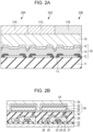
- Fig. 2A and 2B are schematic cross sectional views illustrating examples of a display apparatus that includes organic light emitting elements of the present disclosure and transistors connected to the organic light emitting elements.
- Fig. 2A illustrates one example of a pixel which is a constitutional feature of the display apparatus of this embodiment.
- the pixel has subpixels 20.
- the subpixels are classified as 20R, 20G, and 20B according to their emission color.
- the emission color may be distinguished by the wavelength of the light emitted from the light emission layer, or a color filter or the like may be used to selectively transmit or change the color of the light emitted from the subpixels.
- Each of the subpixels has a first electrode 12 that serves as a reflection electrode disposed on an interlayer insulating layer 11, an insulating layer 13 that covers edges of the first electrode 12, an organic compound layer 14 that covers the first electrode 12 and the insulating layer 13, a second electrode 15, a protection layer 16, and a color filter 17.
- the first electrode 12, the organic compound layer 14, and the second electrode 15 constitute an organic light emitting element 18 of this embodiment.
- the interlayer insulating layer 11 may have a transistor and a capacitor element below or inside thereof.
- the transistor and the first electrode 12 may be electrically connected to each other via a contact hole or the like not illustrated in the drawing.
- the insulating layer 13 is also referred to as a bank or a pixel isolation film.
- the insulating layer 13 covers the edges of the first electrode 12 and surrounds the first electrode 12.
- the part where the insulating layer 13 is absent is in contact with the organic compound layer 14 and functions as a light-emitting region.
- the second electrode 15 may be a transparent electrode, a reflection electrode, or a semi-transmissive electrode.
- the protection layer 16 reduces penetration of moisture into the organic compound layer 14. Although the protection layer 16 is depicted as one layer in the drawing, the protection layer 16 may include multiple layers. An inorganic compound layer and an organic compound layer may be provided for each layer.
- the color filters 17 are classified as 17R, 17G, and 17B according to their colors.
- the color filters may be formed on a planarizing film not illustrated in the drawing.
- a resin protection layer not illustrated in the drawing may be disposed on the color filters.
- the color filters 17 may be formed on the protection layer 16.
- the color filters 17 may be formed on a counter substrate such as a glass substrate and then bonded with the substrate.
- a display apparatus illustrated in Fig. 2B includes an organic light emitting element 36 and a TFT 28 as one example of the transistor. Specifically, there are a substrate 21, such as glass or silicon, and an insulating layer 22 on top of the substrate 21, and a TFT 28 that includes a gate electrode 23, a gate insulating film 24, a semiconductor layer 25, a drain electrode 26, and a source electrode 27 is disposed on the insulating layer 22. An insulating film 29 is disposed on top of the TFT 28, and a contact hole 30 formed in the insulating film 29 connects an anode 31 of the organic light emitting element 36 to the source electrode 27.
- the type of electrical connection between the electrodes (anode 31 and cathode 33) included in the organic light emitting element 36 and the electrodes (source electrode 27 and drain electrode 26) included in the TFT 28 is not limited to the one illustrated in Fig. 2B . In other words, the type of electrical connection may be any as long as one of the anode 31 and the cathode 33 is electrically connected to one of the source electrode 27 and the drain electrode 26.
- the TFT 28 is a thin film transistor.
- a first protection layer 34 and a second protection layer 35 are disposed on the cathode 33 to reduce deterioration of the organic light emitting element.
- the emission luminance of the organic light emitting element 36 of the present embodiment is controlled by the TFT 28, and, by providing multiple organic light emitting elements 36 in-plane, an image can be displayed by using emission luminance.
- the display apparatus illustrated in Fig. 2B uses a transistor as a switching element, but may use a different switching element instead.
- the transistor used in the display apparatus illustrated in Fig. 2B is not limited to a TFT having an active layer on an insulating surface of a substrate and may be a transistor that uses a single-crystal silicon wafer.
- the active layer may be a non-single-crystal silicon such as amorphous silicon or microcrystalline silicon, or a non-single-crystal oxide semiconductor such as indium zinc oxide or indium gallium zinc oxide.
- a transistor made of a low-temperature polysilicon or an active matrix driver formed on a substrate such as a Si substrate may be used.
- the phrase "on the substrate” can also mean “in the substrate”. Whether a transistor is formed in the substrate or a TFT is used is selected according to the size of the display unit; for example, when the size is about 0.5 inches, organic light emitting elements may be formed on a Si substrate.
- the phrase "formed in the substrate” means that the transistor is produced by processing a substrate, such as a Si substrate, itself.
- transistor in the substrate can also be considered as that the substrate and the transistor are integrated.
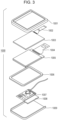
- FIG. 3 is a schematic diagram illustrating one example of the display apparatus according to the present disclosure.
- a display apparatus 1000 includes an upper cover 1001 and a lower cover 1009, and a touch panel 1003, a display panel 1005, a frame 1006, a circuit substrate 1007, and a battery 1008 that are interposed between these covers.
- the touch panel 1003 and the display panel 1005 are respectively connected to flexible print circuits FPC 1002 and 1004. Transistors are printed on the circuit substrate 1007.
- the battery 1008 may be omitted, and even when the display apparatus is a portable appliance, the battery 1008 may be provided at a different position.
- the display apparatus of the present embodiment may include red, green and blue color filters.
- the color filters may be arranged so that red, green and blue are arranged in a delta matrix.
- the display apparatus of the present embodiment is used in a display unit of a portable terminal.
- a display apparatus may have both a display function and an operation function.
- Examples of the portable terminal include mobile phones such as smart phones, tablets, and head-mount displays.
- the display apparatus of the present embodiment is used in a display unit of an imaging apparatus that includes an optical unit having multiple lenses, and an imaging element that receives light that has passed through the optical unit.
- the imaging apparatus may include a display unit that displays the information acquired by the imaging element.
- the display unit may be exposed to the outside of the imaging apparatus or may be disposed in a finder.
- the imaging apparatus may be a digital camera or a digital camcorder.
- FIG. 4A is a schematic diagram illustrating one example of an imaging apparatus according to the present disclosure.
- An imaging apparatus 1100 includes a view finder 1101, a rear display 1102, an operation unit 1103, and a casing 1104.
- the view finder 1101 includes the display apparatus according to the present embodiment.
- the display apparatus may display not only the image to be captured but also the environment information, imaging instructions, etc.
- the environment information may include the intensity of external light, the direction of the external light, the speed in which a photographic subject moves, and a possibility of the photographic subject becoming shielded by a shielding member.
- a display apparatus that uses the organic light emitting element of the present disclosure can be used. This is because the organic light emitting element has a high response speed.
- a display apparatus that uses an organic light emitting element is preferred over a liquid crystal display apparatus for the use in such devices required to achieve speedy display.
- the imaging device 1100 includes an optical unit not illustrated in the drawing.
- the optical unit has multiple lenses, and an image is focused on the imaging element contained in the casing 1104.
- the multiple lenses can adjust the focal point by adjusting the relative positions thereof. This operation can be automated.
- the imaging apparatus may also be referred to as a photoelectric conversion apparatus.
- the photoelectric conversion apparatus can employ an imaging method that involves a method for detecting the difference from a previous image, a method for always cutting out an image from a recorded image, or the like instead of sequential imaging.
- Fig. 4B is a schematic diagram illustrating one example of electronic equipment according to the present disclosure.
- Electronic equipment 1200 includes a display unit 1201, an operation unit 1202, and a casing 1203.
- the casing 1203 may include a circuit, a print substrate having the circuit, a battery, and a communication unit.
- the operation unit 1202 may be a button or a touch panel-system sensitive unit.
- the operation unit may be a biometric unit that performs, for example, unlocking through fingerprint recognition.
- the electronic equipment that includes the communication unit can also be called communication equipment.
- the electronic equipment may further have a camera function when equipped with a lens and an imaging element. The image captured through the camera function is displayed on the display unit. Examples of the electronic equipment include smart phones and laptop computers.
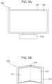
- Figs. 5A and 5B are schematic diagrams illustrating some examples of the display apparatus according to the present disclosure.
- Fig. 5A illustrates a display apparatus such as a television monitor or a PC monitor.
- a display apparatus 1300 includes a frame 1301 and a display unit 1302. The light emitting apparatus of the present disclosure is be used in the display unit 1302.
- the display apparatus 1300 further includes a base 1303 that supports the frame 1301 and the display unit 1302.
- the base 1303 is not limited to the type illustrated in Fig. 5A .
- the lower edge of the frame 1301 may also serve as the base.
- the frame 1301 and the display unit 1302 may be curved.
- the radius of curvature thereof may be 5000 mm or more and 6000 mm or less.
- Figs. 5B is a schematic diagram illustrating another example of the display apparatus according to the present disclosure.
- a display apparatus 1310 illustrated in Fig. 5B is bendable, in other words, a foldable display apparatus.
- the display apparatus 1310 includes a first display unit 1311, a second display unit 1312, a casing 1313, and an inflection point 1314.
- the first display unit 1311 and the second display unit 1312 each include a light emitting apparatus of the present disclosure.
- the first display unit 1311 and the second display unit 1312 may constitute one seamless display apparatus.
- the first display unit 1311 and the second display unit 1312 can be separated at the inflection point.
- the first display unit 1311 and the second display unit 1312 may display different images, or may together display one image.
- FIG. 6A is a schematic diagram illustrating one example of a lighting apparatus according to the present disclosure.
- a lighting apparatus 1400 includes a casing 1401, a light source 1402, a circuit substrate 1403, an optical filter 1404, and a light diffusing unit 1405.
- the light source 1402 includes an organic light emitting element of the present disclosure.
- the optical filter 1404 may be a filter that improves the color rendering properties of the light source.
- the light diffusing unit 1405 can effectively diffuse light from the light source 1402, such as for lighting up, and can deliver the light to a wide range.
- the optical filter 1404 and the light diffusing unit 1405 may be disposed on the light emitting side of the lighting. If necessary, a cover may be provided on the outermost side.
- the lighting apparatus is, for example, an apparatus that illuminates the room.
- the lighting apparatus may emit light that is white, neutral white, or any color from blue to red.
- the lighting apparatus may also include a light modulating circuit that modulates these types of light.
- the lighting apparatus includes an organic light emitting element of the present disclosure and a power supply circuit connected to the organic light emitting element.
- the power supply circuit is a circuit that converts AC voltage into DC voltage.
- White is a color that has a color temperature of 4200 K and the neutral white is a color that has a color temperature of 5000 K.
- the lighting apparatus may include a color filter.
- the lighting apparatus of the present disclosure may include a heat releasing unit.
- the heat releasing unit is a unit that releases the heat inside the apparatus to the outside of the apparatus, and examples thereof include metals having a high specific heat, and liquid silicone.
- Fig. 6B is a schematic diagram of an automobile which is one example of a moving body according to the present disclosure.
- the automobile includes a tail lamp, which is one example of a lighting unit.
- An automobile 1500 includes a tail lamp 1501 and may turn on the tail lamp upon braking operation or the like.
- the tail lamp 1501 includes an organic light emitting element of the present disclosure.
- the tail lamp may also include a protection member that protects the organic light emitting element.
- the protection member may be composed of any material that has a sufficiently high strength and is transparent, and can be composed of polycarbonate or the like.
- the polycarbonate may be mixed with a furandicarboxylic acid derivative, an acrylonitrile derivative, or the like.
- the automobile 1500 may include a car body 1503 and a window 1502 attached to the car body 1503.
- the window may be a transparent display if not a window for checking the front and rear sides of the automobile.
- This transparent display may include an organic light emitting element according to the present disclosure. In such a case, the materials constituting the electrodes, etc., of the organic light emitting element are transparent.
- the moving body according to the present disclosure may be a ship, an airplane, a drone, or the like.
- the moving body includes a body and a lighting unit attached to the body.
- the lighting unit emits light to indicate the position of the body.
- the light unit includes an organic light emitting element of the present disclosure.
- the display apparatus can be applied to wearable device systems such as smart glasses, HMD, and smart contact lenses.
- An imaging display apparatus used in such application examples includes an imaging apparatus capable of converting visible light into electricity, and a display apparatus capable of emitting visible light.
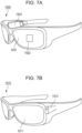
- Fig. 7A illustrates glasses 1600 (smart glasses) according to one application example.
- An imaging apparatus 1602 such as a CMOS sensor or SPAD is disposed on a front side of a lens 1601 of the glasses 1600.
- the display apparatus according to any of the embodiments described above is disposed on a rear side of the lens 1601.
- the glasses 1600 further include a controller 1603.
- the controller 1603 functions as a power supply that supplies power to the imaging apparatus 1602 and the display apparatus of the embodiment.
- the controller 1603 also controls the operation of the imaging apparatus 1602 and the display apparatus.
- An optical system for focusing light onto the imaging apparatus 1602 is formed in the lens 1601.
- Fig. 7B illustrates glasses 1610 (smart glasses) according to one application example.
- the glasses 1610 include a controller 1612, and the controller 1612 includes an imaging apparatus that corresponds to the imaging apparatus 1602 illustrated in Fig. 7A , and a display apparatus.
- a lens 1611 an optical system for projecting light emitted from the display apparatus and the imaging apparatus in the controller 1612 is formed, and images are projected onto the lens 1611.
- the controller 1612 functions as a power supply that supplies power to the imaging apparatus and the display apparatus, and also controls the operation of the imaging apparatus and the display apparatus.
- the controller 1612 may include a line-of-sight detecting unit that detects the line of sight of a wearer. The line of sight may be detected by using infrared radiation.
- the infrared radiation emitting unit emits infrared radiation toward an eyeball of a user gazing the displayed image.
- a captured image of the eyeball is obtained when the imaging unit having a light receiving element detects reflection of the emitted infrared radiation from the eyeball.
- the degradation of the image quality is decreased by providing a unit for reducing light from the infrared radiation emitting unit to the display unit in a plan view.
- the line of sight of the user with respect to the displayed image is detected from the captured image of the eyeball obtained by infrared imaging. Any known technique can be applied to the line-of-sight detection using the captured image of the eyeball. For example, a line-of-sight detection method based on a Purkinje image formed by reflection of the irradiated light at the cornea can be employed. More specifically, a line-of-sight detection process based on the pupil-corneal reflection method is performed. The line of sight of the user is detected by calculating the eye vector that indicates the direction (rotation angle) of the eyeball on the basis of the image of the pupil and the Purkinje image included in the captured image of the eyeball by using the pupil-corneal reflection method.
- the display apparatus of the present disclosure may include an imaging apparatus that includes a light receiving element, and may control the image displayed on the display apparatus on the basis of the line-of-sight information of the user from the imaging apparatus. Specifically, in the display apparatus, a first view region that the user gazes and a second view region other than the first view region are determined on the basis of the line-of-sight information. The first view region and the second view region may be determined by the controller in the display apparatus, or may be determined by an external controller and received. In the display region of the display apparatus, the display resolution of the first view region may be controlled to be higher than the display resolution of the second view region. In other words, the resolution of the second view region may be lower than that of the first view region.
- the display region has a first display region and a second display region different from the first display region, and a region having a higher priority is determined from the first display region and the second display region on the basis of the line-of-sight information.
- the first display region and the second display region may be determined by the controller in the display apparatus, or may be determined by an external controller and received.
- the resolution of the region with higher priority may be controlled to be higher than the resolution of the region other than the region with higher priority. In other words, the resolution of a region having relatively low priority may be decreased.
- An AI may be used to determine the first view region or the region with high priority.
- the AI may be a model configurated to estimate the angle of the line of sight and the distance to the object at the end of the line of sight from the image of the eyeball by using, as teaching data, the image of the eyeball and the direction in which the eyeball in the image was actually gazing.
- the AI program may be included in the display apparatus, the imaging apparatus, or an external apparatus. When an external apparatus includes the AI program, the data is transmitted to the display apparatus via communication.
- smart glasses that further include an imaging apparatus that captures the images of the outside can be implemented.
- the smart glasses can display the captured outside information in real time.
- FIG. 8A is a schematic diagram illustrating one example of an image forming apparatus according to one embodiment of the present disclosure.
- An image forming apparatus 1700 is an electrophotographic image forming apparatus and includes a photosensitive drum 1707, an exposure light source 1708, a charging unit 1710, a developing unit 1711, a transferring device 1712, a conveying roller 1713, and a fixing device 1715.
- Light 1709 is emitted from the exposure light source 1708, and an electrostatic latent image is formed on a surface of the photosensitive drum 1707.
- the exposure light source 1708 includes the organic light emitting element of the present disclosure.
- the developing unit 1711 includes a toner etc.
- the charging unit 1710 charges the photosensitive drum 1707.
- the transferring device 1712 transfers a developed image onto a recording medium 1714.
- the conveying roller 1713 conveys the recording medium 1714.
- the recording medium 1714 is, for example, a sheet of paper.
- the fixing device 1715 fixes the image formed on the recording medium 1714.
- Figs. 8B and 8C are schematic diagrams illustrating the exposure light source 1708 in which light emitting units 1726 are arranged on a long substrate.
- the arrow 1727 indicates the direction parallel to the axis of the photosensitive body as well as the direction in which rows of the organic light emitting elements are arranged. This row direction is coincident with the axis of rotation of the photosensitive drum 1707. This direction can also be referred to as the longitudinal axis direction of the photosensitive drum 1707.
- Fig. 8B is an arrangement in which the light emitting units 1726 are arranged along the longitudinal axis direction of the photosensitive drum 1707.
- Fig. 8C illustrates an arrangement different from the one illustrated in Fig.
- the light emitting units 1726 in the first row and the second row are staggered.
- the first row and the second row are at different positions in the column direction.
- the first row includes multiple light emitting units 1726 with spaces therebetween.
- the second row includes light emitting units 1726 at positions corresponding to the spaces between the light emitting units 1726 in the first row.
- multiple light emitting units 1726 are arranged to be spaced from each other in the column direction also.
- the arrangement illustrated in Fig. 8C can also be referred to as a grid arrangement state, a houndstooth pattern, or a checkered pattern.
- Fig. 9 is a schematic diagram illustrating one form of a light emitting device related to the present embodiment.
- the light emitting device of this embodiment can be used as, for example, a light source of an electrophotographic image forming apparatus.
- the light emitting device of this embodiment has a rectangular shape with long sides parallel to a first direction and short sides parallel to a direction intersecting the first direction, and the first direction may be, for example, a direction extending along the rotation axis direction of a photosensitive body of an image forming apparatus.
- a substrate 1801 has a polygonal shape, and, here, an example in which the substrate 1801 has a rectangular shape is described.
- the long side direction of the rectangular substrate 1801 is referred to as the first direction
- the short side direction orthogonal to the long side direction is referred to as the second direction.
- a polygonal shape includes a shape having rounded corners.
- a moisture proof ring 1800 that reduces penetration of moisture into the light emitting device is disposed on the rectangular substrate 1801.
- the moisture proof ring 1800 can be a guard ring constituted by a wiring layer.
- a light emitting region 1802, a contact region 1803, a pad 1804, and a circuit 1806 are disposed within the moisture proof ring 1800.
- the contact region 1803 includes a first contact region 1803_1, a second contact region 1803_2, and a third contact region 1803_3.
- the pad 1804 includes a first pad 1804_1, a second pad 1804_2, and a third pad 1804_3.
- the circuit 1806 is one of the circuits that drive light emitting devices. Specific examples thereof include, but are not limited to, an input protection circuit, an input circuit through which data for driving is input, and a logic circuit for data processing.
- the contact region 1803 is a region where lines that electrically connect to a common electrode of the light emitting elements EL are disposed.
- the pad 1804_1 electrically connects the contact region 1803 to an external element.
- the contour of the moisture proof ring 1800 may include multiple recessed portions. These portions can be used, for example, as contact regions where ribs of a mask for a vapor deposition step come into contact in the film forming step.
- Each of the multiple light emitting elements EL arranged in a matrix in the light emitting region 1802 includes, as described above, a light emission layer and a first electrode and a second electrode that sandwich the light emission layer.
- the first electrode is an independent electrode provided for each of the light emitting elements EL and the second electrode is a common electrode shared by the light emitting elements EL is described.
- the starting position of the second row of the light emitting elements EL may be shifted in the X direction from the starting position of the first row of the light emitting elements EL by a quarter of the dimension of the light emitting element EL in the X direction.
- n is an integer of 2 or more and n rows are formed, the starting position of the second row of the light emitting elements EL may be shifted in the X direction from the starting position of the first row of the light emitting elements EL by 1/n of the dimension of the light emitting element EL in the X direction.
- the contact region 1803 is an adjacent region to the light emitting region 1802 of the substrate 1801 and is disposed within the moisture proof ring 1800. Furthermore, at least one of the first contact region 1803, the pad 1804, and the circuit region 1806 may be disposed, together with the recessed portions of the moisture proof ring 1800, between the light emitting region 1802 and one of the long side edges of the substrate 1801 in a straight line with respect to the long side direction.
- the contact region 1803, the pad 1804, the circuit region 1806, etc. are disposed at the same position in the short side direction, the length of the light emitting device in the short side direction can be decreased, and the light emitting device can be miniaturized.
- the light emitting device of this embodiment has, along the long side edge of the light emitting device, multiple contact regions 1803 where the common electrode for the light emitting elements EL contacts the power supply line.
- the common electrode is composed of a transparent electrode material having a relatively high electrical resistance
- the voltage drop may increase in the longitudinal axis direction.
- the voltage applied to each OLED varies depending on the distance from the contact region where the potential is supplied.
- the OLEDs to which a voltage for causing light emission of the same luminance is applied may actually emit light with different luminances, and thus shading or the like would occur.
- the voltage drop at the common electrode in the long side direction can be reduced, and occurrence of shading or the like can be reduced.
- Fig. 10A is a schematic perspective view of the head substrate 1900.
- Fig. 10B illustrates the arrangement of multiple light emitting elements EL in the head substrate 1900, and
- Fig. 10C is an enlarged view of one portion of Fig. 10B .
- LED chips 1903 are mounted onto the head substrate 1900.
- the light-emitting device illustrated in Figs. 8A to 8C can be used as the LED chips 1903.
- LED chips 1903 are disposed on one surface of the head substrate 1900, and a long flexible flat cable (FFC) connector 1907 is disposed on the other surface of the head substrate 1900.
- the one surface of the head substrate 1900 is a surface (upper surface or surface) on which the LED chips 1903 are disposed.
- the other surface of the substrate is the surface (lower surface or rear surface) opposite of the surface on which the LED chips 1903 are disposed.
- the FFC connector 1907 is attached to the other surface (lower surface or rear surface) of the head substrate 1900 so that the longitudinal direction thereof extends in the longitudinal direction of the head substrate 1900.
- the long FFC connector 1907 is provided to input control signals (driving signals) from a control circuit unit of the main body of the image forming apparatus, and the control signals are transferred to the LED chips 1903.
- the LED chips 1903 are driven (operation of turning light ON and OFF) by control signals input to the head substrate 1900.
- LED chips 1903 mounted on the head substrate 1900 will now be described.
- multiple light emitting elements EL are disposed on one surface of the head substrate 1900.
- LED chips 1903-1 to 1903-29 (29 chips) are provided.
- the LED chips 1903_1, 1903_13, 1903_14, 1903_15, 1903_16, and 1903_29 are illustrated as examples.
- multiple light emitting elements EL are arranged in its longitudinal direction, and, for example, 516 light emitting elements EL are provided.
- the center-to-center distance k2 between the adjacent light emitting elements EL corresponds to the resolution of the image forming apparatus.
- the resolution of the image forming apparatus of this embodiment is 1200 dpi
- the light emitting elements EL are arranged so that the center-to-center distance k2 between the adjacent light emitting elements EL is 21.16 ⁇ m in the longitudinal direction of the LED chips 1903-1 to 1903-29.
- the exposure range of the exposure head of this embodiment is about 314 mm.
- the photosensitive layer of the photosensitive drum has a width of 314 mm or more. Since the length of the long side of an A4-size recording sheet and the length of the short side of an A3-size recording sheet are 297 mm, the exposure head of this embodiment has an exposure range with which images can be formed on A4-size recording sheets and A3-size recording sheets.
- light emitting elements EL may be arranged in the transverse direction as well as in the longitudinal direction.
- LED chips 1903-1 to 1903-29 are arranged in the axis direction of the photosensitive drum. Specifically, the LED chips 1903-1 to 1903-29 are arranged in two staggered rows along the axis direction of the photosensitive drum. In other words, as illustrated in Fig. 10B , when counted from the left, the odd-numbered LED chips 1903-1, 1903-3, ..., and 1903-29 are mounted in one row in the longitudinal direction of the substrate 1900. When counted from the left, the even-numbered LED chips 1903-2, 1903-4, ..., and 1903-28 are mounted in one row in the longitudinal direction of the substrate 1900. The LED chips 1903 are arranged in such a manner.
- the center-to-center distance k1 of the light emitting elements EL and the center-to-center distance k2 of the light emitting elements EL can be equal to each other.
- the center-to-center distance k1 of the light emitting elements EL is the center-to-center distance between the light emitting element EL at one end of the LED chip 1903_13 and the light emitting element EL at one end of the LED chip 1903_14.
- the center-to-center distance k2 of the light emitting elements EL is the center-to-center distance between the light emitting elements EL that are adjacent to each other in the LED chip 1903_14.
- the center-to-center distance k1 between the light emitting element EL at one end of one LED chip 1903 and the light emitting element EL at one end of another LED chip 1903 that are adjacent to each other can be made equal to the center-to-center distance k2 of the adjacent light emitting elements EL in the same LED chip 1903.
- the light emitting elements EL are organic light emitting elements of a current-driven type.
- the organic light emitting elements are, for example, arranged on a line along the main scanning direction (the axis direction of the photosensitive drum 1707) on a thin film transistor (TFT) substrate, and are electrically connected in parallel through a power supply line formed along the main scanning direction.
- TFT thin film transistor
- the longitudinal direction -to-transverse direction ratio of the shape of the light emitting region 1802 is larger than when the light emitting device is used in a display apparatus or the like.
- the shape of the substrate for the LED chips also has a large longitudinal direction -to-transverse direction ratio.
- the length of the long side of the LED chip can be at least five times or at least 10 times larger than the length of the short side of the LED chip (or the light emitting region 1802).
- the length of the long side of the LED chip can be at least twenty times larger than the length of the short side of the LED (or the light emitting region 1802).
- the length of the long side of the LED chips is determined by the length of the photosensitive drum 1707 in the axis direction, the number of LED chips arranged in the axis direction, and the pattern in which the LED chips 1903 are arranged. Furthermore, the length of the short side of the LED chip 1903 is determined by whether the light emitting elements EL are disposed in the light emitting region 1802 in a direction perpendicular to the axis of the photosensitive drum 1707 or by the arrangement of the pad 1804 and the contact region 1803.
- the light emitting unit 1726 may include a light emission layer that emits red light in view of dependency of the photosensitivity of the photosensitive drum 1707 on the wavelength.
- the LED chips 1803 may include color filters.
- the color filters can absorb stray light from unintended directions without reducing the amount of regular light incident on the photosensitive drum, and thus the printing quality can be improved.
- the disclosure of the present embodiments includes the following features.
- An organic light emitting element including: an anode; a cathode; a light emission layer that is disposed between the anode and the cathode, contains a host material and a light emitting dopant material, and has an anode side facing the anode and a cathode side facing the cathode; a first organic compound layer in contact with the anode side of the light emission layer; and a second organic compound layer in contact with the cathode side of the light emission layer, wherein formulae (1), (2-1), and (2-2) are satisfied: ⁇ 1 H ⁇ ⁇ 2 E HOMOh ⁇ HOMOd LUMOh > LUMOd
- a display apparatus including a plurality of pixels, wherein at least one of the plurality of pixels includes the organic light emitting element of any one of features 1 to 8 and a transistor connected to the organic light emitting element.
- a photoelectric conversion apparatus including: an optical unit that includes a plurality of lenses; an imaging element that receives light that has passed through the optical unit; and a display unit that displays an image taken by the imaging element, wherein the display unit includes the organic light emitting element of any one of features 1 to 8.
- Electronic equipment including: a display unit that includes the organic light emitting element of any one of features 1 to 8; a casing in which the display unit is installed; and a communication unit that is installed in the casing and communicates with outside.
- a lighting apparatus including: a light source that includes the organic light emitting element of any one of features 1 to 8; and a light diffusing unit or an optical filter that transmits light emitted from the light source.
- a moving body including: a lighting unit that includes the organic light emitting element of any one of features 1 to 8; and a body that includes the lighting unit.
- An image forming apparatus including: a photosensitive body; and an exposure light source that exposes the photosensitive body to light, wherein the exposure light source includes the organic light emitting element of any one of features 1 to 8.
- the energy E(eV) of a bandgap (hereinafter referred to as "B.G.") was calculated from the measurement of the HOMO levels of the host materials and the light emitting dopant materials in the light emission layers used in Examples and Comparative Examples and measurement of the wavelengths ⁇ (nm) of the absorption edge of an absorption spectrum.
- the absorption spectrum peak wavelength ⁇ (nm) is converted into the B.G. energy value E(eV) by formula (4) below:
- E eV hc / e ⁇ ⁇ 10 9 (Here, h represents a Planck's constant, c represents the speed of light, and e represents the elementary charge.)
- the HOMO level was measured by using an atmospheric photoelectron spectrometer (trade name: AC-3 produced by RIKEN KEIKI CO., LTD.). The results are indicated in Table 1.
- Table 1 Compound HOMO (eV) B.G.
- mobility measurement elements were prepared by the following method.
- a first organic compound layer or a second organic compound layer was formed into a film thickness of 2 ⁇ m by vapor deposition.
- a 150 nm thick aluminum film was formed by a vacuum evaporation process.
- a protection glass was overlaid thereon in a nitrogen atmosphere, and an UV adhesive was applied and cured. As a result, mobility measurement elements were obtained.
- the hole mobility ⁇ 1H of the first organic compound layer and the electron mobility ⁇ 2E of the second organic compound layer 6 could be measured.
- a time-of-flight measurement instrument TOF-301 produced by OPTEL Co., LTD.
- TOF-301 produced by OPTEL Co., LTD.
- an organic light emitting element having a layer configuration illustrated in Fig. 1A was prepared by the following method.
- a 40 nm-thick titanium (Ti) film was formed as an anode 2 on a silicon substrate by a sputtering method and was photolithographically patterned so as to form regular hexagonal-Ti pixel array and wiring with a pixel pitch of 4.2 ⁇ m.
- a silicon nitride (SiN) insulating layer was formed on Ti and was photolithographically patterned so as to form a pixel array exposing Ti while the width of the SiN insulating layer that partitioned the pixels was 1 ⁇ m.
- the water-washed substrate with the layers up to the insulating layer formed thereon, and the materials placed in a molybdenum or tungsten vapor deposition boat were installed in a vacuum vapor deposition apparatus, and UV/ozone washing was performed.
- films were formed into a layer configuration indicated in Table 3 below, and the resulting substrate was transferred to a glove box and sealed with a desiccant-containing glass cap in a nitrogen atmosphere to obtain an organic light emitting element.
- a voltage source was connected to the obtained organic light emitting element to evaluate the characteristics of the organic light emitting element.
- the voltage-current characteristic was measured with a pico ammeter 4140B produced by Hewlett-Packard Company, and the emission spectrum and the emission luminance were acquired by using SR-3 produced by TOPCON TECHNOHOUSE CORPORATION.
- the driving voltage used to emit light having a luminance of 3000 cd/m 2 was 3.2 V.
- This element was continuously driven in a dry air atmosphere while keeping the luminance at a current density of 1600 mA/cm 2 , and the time (LT95) taken for the initial emission luminance to drop to 95% was as long as 400 hours.
- the organic light emitting element exhibited good durability lifetime and low voltage.
- the obtained multilayer organic light emitting element satisfied the feature 1 of the present disclosure described above and the optional features 2 to 7 described above.
- Organic light emitting elements were prepared as in Example 1 except that the host material, the light emitting dopant material, and the materials for the first organic compound layer and the second organic compound layer of Example 1 were changed to the materials indicated in Table 4. AD-25 used in the second organic compound layer in Comparative Example 1 and HT14 used in the first organic compound layer in Comparative Example 2 are indicated below.
- Example 1 HT1 H4 RD9 AD-2 3.2 400
- Example 2 HT2 H1 RD11 AD-9 3.5 380
- Example 3 TH3 H3 RD20 AD-1 3.6
- Example 4 HT6 H10 RD8 AD-7 3.8
- Example 5 HT2 H4 RD20 AD-2 3.7 410
- Example 6 HT3 H1 RD9 AD-7 3.3 400
- Example 7 HT1 H3 RD11 AD-9 3.6 380
- Example 9 HT3 H3 RD8 AD-19 4.2
- Example 10 HT1 H1 RD9 AD-23 4.5 430
- Example 11 HT3 H4 RD4 AD-2 3.7 300
- Example 12 HT2 H3 RD1 AD-15 4.5
- the organic light emitting elements of Examples that satisfy the feature 1 of the present disclosure has a low driving voltage and long durability lifetime.
- the organic light emitting elements of Examples 1 to 10 that have features 2 to 7 yielded good results.
- the tendency of low voltage is approximately a reflection of the difference in HOMO level between the host material and the light emitting dopant material and the value of the electron mobility ⁇ 2E of the second organic compound layer.
- the LT95 durability lifetime is approximately a reflection of the difference between the hole mobility ⁇ 1H of the first organic compound layer and the electron mobility ⁇ 2E of the second organic compound layer, and organic light emitting elements having low voltage and good durability lifetime are obtained.
- the element of Comparative Example 1 had poor durability lifetime. The reason for this is considered that because ⁇ 1H ⁇ ⁇ 2E in Comparative Example 1, the exciton generating region shifted toward the amine bond-containing first organic compound layer, the light emission layer became unstable against radical cations generated by further recombination of the generated excitons and holes, and thus deterioration of the light emission layer was accelerated.
- the driving voltage was higher than the elements of Examples, and the durability lifetime was also poor.
- the reason for this is considered that because ⁇ 1H ⁇ ⁇ 2E, the exciton generating region shifted toward the amine bond-containing first organic compound layer, the light emission layer became unstable against radical cations generated by further recombination of the generated excitons and holes, and thus deterioration of the light emission layer was accelerated.
- HT14 has one less amine structure than HT1 and has a carbazole skeleton instead, the HOMO level was lower, and presumably thus the hole injection barrier from the anode side was raised and the voltage increased.
- the driving voltage was higher than the elements of Examples, and the durability lifetime was also poor.
- the HOMO level of the host material AD-14 was higher than the HOMO level of the light emitting dopant material AD-21 and thus formula (2-1) was not satisfied.
- the hole injectability from the first organic compound layer to the light emission layer decreased notably, and thus the voltage increased.
- the exciton generating region shifts toward the first organic compound layer, and the first organic compound layer becomes deteriorated. Presumably because of the high driving voltage and accelerated deterioration of the first organic compound layer, the durability lifetime of the element has decreased.
- an organic light emitting element that can be driven at low voltage and that exhibits excellent driving durability is provided.
- an excellent organic light emitting display apparatus that uses such organic light emitting elements can be provided.
- An organic light emitting element that includes an anode (2), a cathode (9), a first organic compound layer (4), a light emission layer (5) containing a host material and a light emitting dopant material, and a second organic compound layer (6).
- the relationships concerning HOMO levels and LUMO levels of the host material and the light emitting dopant material in the light emission layer (5) are specified, and the materials for these layers are selected so that the hole mobility of the first organic compound layer (4) is equal to or greater than the electron mobility of the second organic compound layer (6).
Landscapes
- Physics & Mathematics (AREA)
- Optics & Photonics (AREA)
- Electroluminescent Light Sources (AREA)
Abstract
An organic light emitting element that includes an anode (2), a cathode (9), a first organic compound layer (4), a light emission layer (5) containing a host material and a light emitting dopant material, and a second organic compound layer (6). The relationships concerning HOMO levels and LUMO levels of the host material and the light emitting dopant material in the light emission layer (5) are specified, and the materials for these layers are selected so that the hole mobility of the first organic compound layer (4) is equal to or greater than the electron mobility of the second organic compound layer (6).
Description
- The present disclosure relates to an organic light emitting element, and various appliances and apparatuses that include the organic light emitting element.
- An organic light emitting element (hereinafter, also referred to as an "organic electroluminescence element" or an "organic EL element") is an electronic element that includes a pair of electrodes and an organic compound layer disposed between these electrodes. By injecting electrons and holes from the pair of electrodes, excitons of a light emitting organic compound in the organic compound layer are generated, and the organic light emitting element emits light as the excitons return to the ground state.
- Recent advancement in organic light emitting elements has been remarkable, enabling low drive voltage, a wide variety of emission wavelengths, high-speed responsivity, and thickness and weight reduction of light emitting devices. However, presently, the light emission efficiency and the continuous driving lifetime of the organic light emitting element are not practically sufficient for the element to be used as a light emitting device such a display, and higher light emission efficiency and improved continuous driving lifetime are desirable.
- Regarding the improvement of the continuous driving lifetime of the organic light emitting element,
Japanese Patent Laid-Open No. 2006-270091 -
Japanese Patent Laid-Open No. 2006-270091 - The present disclosure addresses the issues described above and provides an organic light emitting element that is driven at low voltage and has excellent durability properties.
- The present invention in its first aspect provides an organic light emitting element as specified in
claims 1 to 8. The present invention in its second aspect provides a display apparatus as specified inclaim 9. The present invention in its third aspect provides a photoelectric conversion apparatus as specified in claim 10. The present invention in its fourth aspect provides electronic equipment as specified inclaim 11. The present invention in its fifth aspect provides a lighting apparatus as specified inclaim 12. The present invention in its sixth aspect provides a moving body as specified inclaim 13. The present invention in its seventh aspect provides an image forming apparatus as specified inclaim 14. - Further features of the present disclosure will become apparent from the following description of exemplary embodiments with reference to the attached drawings.
-
-
Fig. 1A is a schematic cross-sectional view of one embodiment of an organic light emitting element according to the present disclosure.Fig. 1B is an energy diagram schematically illustrating the energy levels of a light emission layer and adjacent layers in the organic light emitting element according to the present disclosure. -
Fig. 2A is a schematic cross-sectional view of a pixel of a display apparatus according to one embodiment of the present disclosure.Fig. 2B is a schematic cross-sectional view of a display apparatus according to one embodiment of the present disclosure. -
Fig. 3 is a schematic diagram of a display apparatus according to one embodiment of the present disclosure. -
Fig. 4A is a schematic diagram of an imaging apparatus according to one embodiment of the preset disclosure.Fig. 4B is a schematic diagram of electronic equipment according to one embodiment of the present disclosure. -
Fig. 5A is a schematic diagram of a display apparatus according to one embodiment of the present disclosure.Fig. 5B is a schematic diagram of a foldable display apparatus according to one embodiment of the present disclosure. -
Fig. 6A is a schematic diagram of a lighting apparatus according to one embodiment of the present disclosure.Fig. 6B is a schematic diagram of an automobile that includes a vehicle lighting unit according to one embodiment of the present disclosure. -
Fig. 7A is a schematic diagram illustrating one example of a wearable device according to one embodiment of the present disclosure.Fig. 7B is a schematic diagram illustrating one example of a wearable device according to one embodiment of the present disclosure equipped with an imaging apparatus. -
Fig. 8A is a schematic diagram illustrating one example of an image forming apparatus according to one embodiment of the present disclosure,Fig. 8B is a schematic diagram illustrating one example of an exposure light source used therein, andFig. 8C is a schematic diagram illustrating another example of an exposure light source used therein. -
Fig. 9 is a schematic diagram illustrating one example of an exposure light source of an image forming apparatus according to one embodiment of the present disclosure. -
Figs. 10A, 10B, and 10C are schematic diagrams illustrating one example of the exposure light source of the image forming apparatus according to one embodiment of the present disclosure. - An organic light emitting element according to the present disclosure includes an anode, a cathode, a light emission layer that is disposed between the anode and the cathode, contains a host material and a light emitting dopant material, and has an anode side facing the anode and a cathode side facing the cathode, a first organic compound layer in contact with the anode side of the light emission layer, and a second organic compound layer in contact with the cathode side of the light emission layer.
- Furthermore, following formulae (1), (2-1), and (2-2) are satisfied.


- µ1H: the hole mobility of the first organic compound layer
- µ2E: the electron mobility of the second organic compound layer
- HOMOh: the HOMO level of the host material
- LUMOh: the LUMO level of the host material
- HOMOd: the HOMO level of the light emitting dopant material
- LUMOd: the LUMO level of the light emitting dopant material
- The features and embodiments of the present disclosure will now be described.
- 1. Formulae (1), (2-1), and (2-2) are satisfied.
- First, description related to
Figs. 1A and 1B is provided.Fig. 1A is a schematic cross-sectional view illustrating one example of an embodiment of the organic light emitting element of the present disclosure. As illustrated inFig. 1A , in the present disclosure, at least a firstorganic compound layer 4, alight emission layer 5, and a secondorganic compound layer 6 are interposed between ananode 2 and acathode 9. Thelight emission layer 5 contains a host material and a light emitting dopant material. -
Fig. 1B is an energy diagram schematically illustrating the energy levels of thelight emission layer 5, the firstorganic compound layer 4, and the secondorganic compound layer 6 according to the present disclosure. The firstorganic compound layer 4 is in contact with the anode side of thelight emission layer 5, and the secondorganic compound layer 6 is in contact with the cathode side of thelight emission layer 5. - HOMO is short for highest occupied molecular orbital, and the energy level thereof is referred to as a "HOMO level" or "HOMO". LUMO is short for lowest unoccupied molecular orbital and the energy level thereof is referred to as a "LUMO level" or "LUMO". The HOMO level and the LUMO level are negative values, and, when the magnitudes of the energy levels are expressed in the present disclosure, the levels that are coming closer to the vacuum level are referred to as high levels or increased levels, and the levels that are coming farther from the vacuum level are referred to as low levels or decreased levels.
-
Fig. 1B is a typical energy diagram in which the HOMO level of the firstorganic compound layer 4 is higher than the HOMO level of the host material in thelight emission layer 5 and in which the LUMO level of the secondorganic compound layer 6 is lower than the LUMO level of the host material in thelight emission layer 5. - Since the first
organic compound layer 4 has a function of an electron blocking layer, the LUMO level of the firstorganic compound layer 4 is higher than the LUMO level (LUMOh) of the host material, and, when the firstorganic compound layer 4 has a bandgap substantially the same as that of the host material, the HOMO level of the firstorganic compound layer 4 is naturally higher than the HOMO level (HOMOh) of the host material. - In contrast, since the second
organic compound layer 6 has a function of a hole blocking layer, the HOMO level of the secondorganic compound layer 6 is lower than the HOMO level (HOMOh) of the host material, and, when the secondorganic compound layer 6 has a bandgap substantially the same as that of the host material, the LUMO level of the secondorganic compound layer 6 is naturally lower than the LUMO level (LUMOh) of the host material. - As mentioned above, according to the energy diagram illustrated in
Fig. 1B , when thelight emission layer 5 is solely composed of a host material, the relationships indicated by "HOMO level of firstorganic compound layer 4 > HOMO level of host material" and "LUMO level of secondorganic compound layer 6 < LUMO level of host material" are established, and due to these relationships, an injection barrier is present in injecting holes and electrons into thelight emission layer 5 and thus higher voltage is needed. - When formula (2-1) and (2-2) above are satisfied in the
light emission layer 5 as one of the features of the present disclosure, the barrier present during the injection of holes from the firstorganic compound layer 4 into thelight emission layer 5 and the injection of electrons from the secondorganic compound layer 6 into thelight emission layer 5 is alleviated, and thus low voltage is achieved. This is because some of holes and electrons are injected through the HOMO level (HOMOd) and the LUMO level (LUMOd) of the light emitting dopant material illustrated inFig. 1B and thus the injection barrier is alleviated. To facilitate the injection through the LUMO level of the dopant material, the LUMO level of the dopant material can be lower than the LUMO level of the secondorganic compound layer 6. Likewise, to facilitate the injection through the HOMO level of the dopant material, the HOMO level of the dopant material can be higher than the HOMO level of the firstorganic compound layer 4. By employing one of these structures, the effect of voltage reduction is achieved, and by employing both structures, a more preferable embodiment is created. - When the relationship indicated by formula (1) above as well as the relationships indicated by formulae (2-1) and (2-2) are satisfied, the proportion in which the region (hereinafter this region is referred to as the "exciton generating region") where excitons are generated due to recombination of holes and electrons in the
light emission layer 5 occupies the second organic compound layer 6-side portion of thelight emission layer 5 increases, deterioration of thelight emission layer 5 is alleviated, and thus the lifetime of the organic light emitting element can be extended. - The proportion in which the exciton generating region in the
light emission layer 5 occupies the vicinity of the first organic compound layer 4-side interface or the second organic compound layer 6-side interface is typically attributable to the balance between the hole mobility and the electron mobility in thelight emission layer 5 in most cases. Meanwhile, when the hole mobility and the electron mobility are about the same, the exciton generating region in thelight emission layer 5 is affected by the hole mobility (µ1H) of the firstorganic compound layer 4 adjacent to thelight emission layer 5 and the electron mobility (µ2E) of the secondorganic compound layer 6 adjacent to thelight emission layer 5. Here, by satisfying the relationship indicated by formula (1), the hole mobility of the firstorganic compound layer 4 is faster than the electron mobility of the secondorganic compound layer 6, and thus the proportion in which the exciton generating region occupies the second organic compound layer 6-side portion in thelight emission layer 5 increases. - In general, the first
organic compound layer 4 is composed of an amine skeleton-containing material, and, as described below, the amine skeleton-containing material is unstable in terms of bonding energy; thus, when the proportion in which the recombination region occupies the first organic compound layer 4-side portion of thelight emission layer 5 increases, deterioration of thelight emission layer 5 is prone to occur. Here, in such a case, the probability of electron injection from thelight emission layer 5 into the firstorganic compound layer 4 increases, but since the firstorganic compound layer 4 is unstable against electrons, there is a high possibility that the firstorganic compound layer 4 would deteriorate. - Meanwhile, in general, the second
organic compound layer 6 can be composed of a hydrocarbon, which is stable in terms of bonding energy. Thus, when the proportion in which the recombination region occupies the second organic compound layer 6-side portion increases, there is a possibility that hole injection would occur from thelight emission layer 5 into the secondorganic compound layer 6; however, in such a case also, the possibility of deterioration of the secondorganic compound layer 6 is low since the secondorganic compound layer 6 is chemically stable against the holes. - As such, since the second
organic compound layer 6 can be composed of a highly chemically stable material, by satisfying the relationship indicated by formula (1), the proportion in which the exciton generating region in thelight emission layer 5 occupies the second organic compound layer 6-side portion increases, and deterioration of thelight emission layer 5 is reduced. Thus, the lifetime of the organic light emitting element can be extended at the same time as achieving low voltage when the relationships indicated by formulae (1), (2-1), and (2-2) are satisfied. - The organic light emitting element according to the present disclosure can have following
features 2 to 6. - 2. The light emission layer satisfies the relationships indicated by formulae (3-1) and (3-2) below.


- By satisfying the relationships indicated by formulae (3-1) and (3-2), the hole injectability from the first
organic compound layer 4 into thelight emission layer 5 and the electron injectability from the secondorganic compound layer 6 into thelight emission layer 5 are improved and, in addition, the holes and electrons injected into thelight emission layer 5 become trapped in thelight emission layer 5, leakage of holes to the secondorganic compound layer 6 and electrons to the firstorganic compound layer 4 can be reduced. As a result, the hole-electron recombination probability is improved, the exciton generating probability is improved, and thus the light emission efficiency of the organic light emitting element can be improved. - Furthermore, by satisfying the relationships indicated by formulae (3-1) and (3-2), the light emission efficiency is improved and, in addition, the hole mobility and the electron mobility in the
light emission layer 5 become substantially the same. Thus, although the exciton generating region in thelight emission layer 5 is affected by the hole mobility of the firstorganic compound layer 4 adjacent to thelight emission layer 5 and the electron mobility of the secondorganic compound layer 6 adjacent to thelight emission layer 5, the lifetime of the light emitting element can be extended as described above since the relationship indicated by formula (1) is satisfied. - 3. The host material and the light emitting dopant material are hydrocarbons.
- The host material and the light emitting dopant material of the present disclosure can each have a molecular structure that can withstand excessive radical cation generation, and can be highly chemically stable hydrocarbons. A hydrocarbon is a compound that does not have a bond with low bonding stability within its molecular structure, and thus, when the element is driven, the compound rarely undergoes deterioration due to driving, and the lifetime of the organic light emitting element is long. A bond with low bonding stability in the molecular structure refers to a bond, such as an amino group, that has relatively low bonding energy and is unstable.
- Bonds with low bonding stability in compounds A-1, A-2, and B-1 described below are a bond between a carbazole ring and a phenylene group and a bond between an amino group and a phenyl group (nitrogen-carbon bonds). A bond between carbons, such as that in compound B-1, has higher bonding stability.

- Here, calculation was performed by b3-lyp/def2-SV(P).
- A density functional theory (DFT) currently widely used is employed as the molecular orbital calculation technique. B3LYP was used as the functional, and 6-31G* was used as the base function. The molecular orbital calculation was performed by Gaussian09 (Gaussian 09, Revision C.01, M. J. Frisch, G. W. Trucks, H. B. Schlegel, G. E. Scuseria, M. A. Robb, J. R. Cheeseman, G. Scalmani, V. Barone, B. Mennucci, G. A. Petersson, H. Nakatsuji, M. Caricato, X. Li, H. P. Hratchian, A. F. Izmaylov, J. Bloino, G. Zheng, J. L. Sonnenberg, M. Hada, M. Ehara, K. Toyota, R. Fukuda, J. Hasegawa, M. Ishida, T. Nakajima, Y. Honda, O. Kitao, H. Nakai, T. Vreven, J. A. Montgomery, Jr., J. E. Peralta, F. Ogliaro, M. Bearpark, J. J. Heyd, E. Brothers, K. N. Kudin, V. N. Staroverov, T. Keith, R. Kobayashi, J. Normand, K. Raghavachari, A. Rendell, J. C. Burant, S. S. Iyengar, J. Tomasi, M. Cossi, N. Rega, J. M. Millam, M. Klene, J. E. Knox, J. B. Cross, V. Bakken, C. Adamo, J. Jaramillo, R. Gomperts, R. E. Stratmann, O. Yazyev, A. J. Austin, R. Cammi, C. Pomelli, J. W. Ochterski, R. L. Martin, K. Morokuma, V. G. Zakrzewski, G. A. Voth, P. Salvador, J. J. Dannenberg, S. Dapprich, A. D. Daniels, O. Farkas, J. B. Foresman, J. V. Ortiz, J. Cioslowski, and D. J. Fox, Gaussian, Inc., Wallingford CT, 2010.) that is currently widely implemented.
- These results indicate that the host material and the light emitting dopant material in the light emission layer of the present disclosure can be hydrocarbons. Specifically, for example, benzene, naphthalene, fluorene, benzofluorene, phenanthrene, chrysene, triphenylene, pyrene, perylene, fluoranthene, and benzofluoranthene have high intramolecular bonding energy since there are up to two benzene rings that are fused linearly.
- 4. The host material includes a perylene skeleton in its molecular structure.
- As described in 3 above, the host material can be a hydrocarbon having high chemical stability and, in particular, can be a fused polycycle having a particularly narrow bandgap. Due to formulae (2-1) and (2-2), some of holes and electrons are injected through the HOMO level and the LUMO level of the light emitting dopant material and thus the injection barrier is alleviated; however, most of holes and electrons are directly injected to the HOMO level and the LUMO level of the host material. Thus, by selecting a material with a narrow bandgap as the host material, the hole injectability from the first
organic compound layer 4 to thelight emission layer 5 and the electron injectability from the secondorganic compound layer 6 to thelight emission layer 5 are improved, and the voltage can be further decreased. - Specific examples of the fused polycycles of hydrocarbons with narrow bandgaps include, but are not limited to, the following. In particular, those which have structures represented by H1 to H12 having perylene skeletons are particularly preferable.





- 5. Emission color is red.
- The emission color of the organic light emitting element of the present disclosure can be red. This is because when the host material is a highly chemically stable hydrocarbon and can have a narrow bandgap and a perylene skeleton, the light emitting dopant material can be a long-wavelength red light emitting material having a narrow bandgap in order to satisfy the relationships indicated by formulae (3-1) and (3-2).
- Specific examples of the light emitting dopant are as follows.





- 6. The second organic compound layer consists of a hydrocarbon.
- For the same reasons as those described in 3 above, the second organic compound layer can also consist of a highly chemically stable hydrocarbon.
- 7. The electron mobility µ2E of the second organic compound layer is 1 × 10⁻³ cm2/Vs or less, and a pyrene skeleton or a fluoranthene skeleton is contained in the molecular structure.
- The second
organic compound layer 6 can be composed of a fused polycycle having an electron mobility µ2E of 1 × 10⁻³ cm2/Vs or less, and, specifically, can be composed of a material that contains a pyrene skeleton or a fluoranthene skeleton in its molecular structure. Thus, the firstorganic compound layer 4 can be composed of a material having a hole mobility µ1H of 1 × 10⁻³ cm2/Vs or less. - Specific examples of the material constituting the second
organic compound layer 6 are described below, among which AD-1 to AD-12 having an electron mobility µ2E of 1 × 10⁻⁴ cm2/Vs or more and 1 × 10⁻³ cm2/Vs or less are preferable.


- An organic light emitting element is typically obtained by forming an insulating layer, a first electrode, an organic compound layer, and a second electrode on a substrate. A protection layer, a color filter, a microlens, etc., may be formed on the second electrode. When a color filter is to be formed, a planarization layer may be formed between the color filter and the protection layer. The planarization layer can be formed by using an acrylic resin or the like. The same applies to the case in which a planarization layer is formed between a color filter and a microlens.
- The features of the organic light emitting element of the present disclosure other than the light emission layer and the second organic compound layer will now be described.
- The organic light emitting element of the present disclosure may be formed on a substrate, and examples of the substrate include quartz, glass, a silicon wafer, a resin, and a metal. Switching elements such as transistors and lines may be disposed on the substrate, and an insulating layer may be disposed thereon. The material for the insulating layer may be any as long as contact holes that can form lines to the first electrode can be formed and the insulation from the lines not to be connected can be secured. For example, resins such as polyimide, silicon oxide, or silicon nitride can be used.
- The organic light emitting element includes a pair of electrodes, and, when an electric field is applied in a direction in which the organic light emitting element emits light, the electrode with a higher potential is the anode, and the other electrode is the cathode. This can also be rephrased as that the electrode that supplies holes to the light emission layer is the anode, and the electrode that supplies electrons is the cathode. In the present disclosure, one of the anode and the cathode may be a first electrode (substrate-side electrode). Typically, as illustrated in
Fig. 1A , theanode 2 is arranged on thesubstrate 1 side, but this is not limiting. - The material constituting the anode can have a work function as large as possible. Examples of such a material that can be used include single metals such as gold, platinum, silver, copper, nickel, palladium, cobalt, selenium, vanadium, and tungsten, mixtures thereof, and alloys thereof; and metal oxides such as tin oxide, zinc oxide, indium oxide, indium tin oxide (ITO), and indium zinc oxide. In addition, conductive polymers such as polyaniline, polypyrrole, and polythiophene can be used.
- These electrode substances may be used alone or two or more of these substances may be used in combination. The anode may be constituted by a single layer or multiple layers.
- For use as a reflection electrode, chromium, aluminum, silver, titanium, tungsten, molybdenum, an alloy thereof, or a layered product thereof can be used. A reflection film that does not function as an electrode can also be made by using the aforementioned material. For use as a transparent electrode, an oxide transparent conductive layer such as indium tin oxide (ITO) or indium zinc oxide can be used, but this is not limiting. Photolithography can be employed to form electrodes.
- In contrast, the material constituting the cathode can have a small work function. Examples of such a material include alkali metals such as lithium, alkaline earth metals such as calcium, single metals such as aluminum, titanium, manganese, silver, lead, and chromium, and mixtures thereof. In addition, alloys of these single metals can also be used. For example, magnesium-silver, aluminum-lithium, aluminum-magnesium, silver-copper, and zinc-silver can be used. Metal oxides such as indium tin oxide (ITO) can also be used. These electrode substances may be used alone or two or more of these substances may be used in combination. The cathode may have a single layer structure or a multilayer structure. In particular, silver is preferably used, and, in order to decrease aggregation of silver, silver alloys are more preferably used. The alloying ratio may be any as long as aggregation of silver can be decreased. For example, the silver-to-other metal ratio may be 1:1, 3: 1, or the like.
- The cathode is not particularly limited, for example, an oxide conductive layer such as ITO can be used as the cathode to form a top-emission element, or aluminum (Al) or the like can be used in the cathode to function as a reflection electrode so as to form a bottom-emission element. The method for forming the cathode may be any; however, DC or AC sputtering achieves good film coverage and easily decreases the resistance.
- As illustrated in
Fig. 1A , the organic light emitting element of the present disclosure includes thehole injection layer 3, theelectron transport layer 7, theelectron injection layer 8, etc., but these layers are optional and any of these layers may include multiple layers. Furthermore, although these are examples of the organic compound layers, these layers may be composed of inorganic compounds. - Furthermore, various layer configurations may be employed, such as providing an insulating layer at the interface between an electrode and an organic compound layer, providing an adhesion layer or an interference layer, and forming the
electron transport layer 7 or the firstorganic compound layer 4 by using two layers with different ionization potentials. - The organic compound layers may be formed as common layers for multiple organic light emitting elements. A common layer is a layer that straddles over multiple organic light emitting elements, and can be formed by performing a coating method such as spin coating or a vapor deposition method on the entire surface of the substrate.
- Examples of the materials therefor are as follows. Examples of the material used in the first
organic compound layer 4 include materials that facilitate injection of holes from theanode 2 and materials having high hole mobility capable of transporting injected holes to the light emission layer. The same material can be used in thehole injection layer 3. - In order to reduce degradation of the film quality, such as crystallization, in the organic light emitting element, a material with a high glass transition point can be used. Examples of low-molecular-weight and high-molecular-weight materials with high hole mobility include triarylamine derivatives, arylcarbazole derivatives, phenylenediamine derivatives, stilbene derivatives, phthalocyanine derivatives, porphyrin derivatives, poly(vinylcarbazole), poly(thiophene), and other conductive polymers.
- Specific examples of the material used in the first
organic compound layer 4 are described in HT1 to HT9 below, but these examples are not limiting.


- In the
hole injection layer 3, a compound having a deep LUMO level, such as a hexaazatriphenylene compound, a tetrafluoroquinodimethane compound, or a dichlorodicyanobenzoquinone compound, can be used. Specific examples thereof include compounds HT10 to HT13 described below.
- The material for the
electron transport layer 7 can be freely selected from those which can transfer electrons to the light emission layer, and is selected by considering the balance with the hole mobility of the hole transport material, etc. - Examples of the material having the electron transport capacity include oxadiazole derivatives, oxazole derivatives, pyrazine derivatives, triazole derivatives, triazine derivatives, quinoline derivatives, quinoxaline derivatives, phenanthroline derivatives, and organoaluminum complexes.
- Specific examples of the material used in the
electron transport layer 7 are described in ET1 to ET23 below, but these examples are not limiting. A material, such as ET1 to ET7, that has a phenanthroline or pyridine skeleton can be used in theelectron transport layer 7. This is because such a material interacts with an electron injection material such as an alkali metal compound or an electrode material and thus has an effect of decreasing the electron injection barrier.


- In the present disclosure, the
electron injection layer 8 may be included. Any commonly known material can be used in theelectron injection layer 8, and examples thereof include alkali metals, alkaline earth metals, rare earth metals, and compounds thereof. Specifically, metallic Ca, LiF, KF, Cs2CO3, or the like is used, and a mixture of any of these with the aforementioned electron transport materials may be used. - The organic compound layers constituting the organic light emitting element of the present disclosure can be formed by a dry process such as a vacuum deposition method, an ionized deposition method, sputtering, or plasma. Instead of the dry process, a wet process can be employed to form layers by a known coating method (for example, spin coating, dip coating, casting, a LB method, or an inkjet method) that involves dissolving the material in an appropriate solvent.
- Here, when layers are formed by a vacuum deposition method or a solution coating method, for example, crystallization rarely occurs, and stability over time is improved. When films are formed by a coating method, an appropriate binder resin may be used in combination to form the films.
- Examples of the binder resin include, but are not limited to, polyvinyl carbazole resin, polycarbonate resin, polyester resin, ABS resin, acrylic resin, polyimide resin, phenolic resin, epoxy resin, silicone resin, and urea resin.
- These binder resins may be used alone as a homopolymer or in combination as a mixture of two or more to form a copolymer. If necessary, additives such as known plasticizers, oxidation inhibitors, and ultraviolet absorbents may be used in combination.
- A protection layer may be formed on the second electrode. For example, by bonding a hygroscopic agent-laden glass onto the second electrode, penetration of water and the like into organic compound layers can be reduced, and the incidence of display failures can be decreased. In another embodiment, a passivation film such as silicon nitride film may be disposed on the second electrode so as to reduce penetration of water and the like into the organic compound layers. For example, after the second electrode is formed, the second electrode may be transported to another chamber without breaking the vacuum, and then a silicon nitride film having a thickness of 2 µm may be formed thereon by a CVD method to form a protection layer. Alternatively, after film deposition by a CVD method, a protection layer may be formed by an atomic layer deposition (ALD) method. The material for the film formed by the ALD method is not particularly limited and can be silicon nitride, silicon oxide, or aluminum oxide, for example. Silicon nitride may be further formed by a CVD method on the film formed by an ALD method. The film formed by the ALD method may be thinner than the film formed by the CVD method. Specifically, the thickness may be 50% or less or even 10% or less.
- A color filter may be formed on the protection layer. For example, a color filter that takes into account the size of the organic light emitting element may be disposed on a separate substrate, and this substrate may be bonded with the substrate on which the organic light emitting element has been formed, or a color filter may be formed by photolithographic patterning on the aforementioned protection layer. The color filter may be composed of a polymer.
- A planarization layer may be disposed between the color filter and the protection layer. The planarization layer is formed for the purpose of decreasing the irregularities of the underlying layer. Such a layer may also be referred to as a material resin layer without limiting the purpose. The planarization layer may be composed of an organic compound and may have a low molecular weight or a high molecular weight, preferably, a high molecular weight.
- Planarization layers may be disposed above and under the color filter, and in such a case, the materials constituting the planarization layers may be the same or different. Specific examples thereof include polyvinyl carbazole resin, polycarbonate resin, polyester resin, ABS resin, acrylic resin, polyimide resin, phenolic resin, epoxy resin, silicone resin, and urea resin.
- An organic light emitting element or an organic light emitting apparatus that includes the organic light emitting element may include an optical member, such as a microlens, on the light incident side thereof. The microlens can be composed of an acrylic resin, an epoxy resin, or the like. The microlens may be provided for the purposes of increasing the amount of light emerging from the organic light emitting element or the organic light emitting apparatus and controlling the direction in which the light emerges. The microlens may have a hemispherical shape. When the microlens has a hemispherical shape, there are tangent lines that contact the hemisphere, among which there is a tangent line parallel to the insulating layer, and the point of contact between that tangent line and the hemisphere is the apex of the microlens. The apex of the microlens can also be determined in the same manner from any cross-sectional view thereof. In other words, among the tangent lines that contact the semicircle of the microlens in a cross-sectional view, there is a tangent line parallel to the insulating layer, and the point of contact between that tangent line and the semicircle is the apex of the microlens.
- Furthermore, the midpoint of the microlens can be defined. In a cross section of the microlens, a line segment extending from a point where the shape or an arc ends to another point where the shape of the arc ends is hypothetically drawn, and the midpoint of that line segment can be called the midpoint of the microlens. The cross section used to determine the apex and the midpoint may be a cross section perpendicular to the insulating layer.
- A counter substrate may be provided on the planarization layer. The counter substrate is called a counter substrate since the counter substrate is disposed at a position opposing the aforementioned substrate. The material constituting the counter substrate may be the same as the aforementioned substrate. The counter substrate may be a second substrate provided that the aforementioned substrate is a first substrate.
- An organic light emitting apparatus that includes an organic light emitting element may include a pixel circuit connected to the organic light emitting element. The pixel circuit may be of an active matrix type that independently controls light emission of a first light emitting element and a second light emitting element. The active matrix circuit may be voltage-programmed or current-programmed. The drive circuit has a pixel circuit for each pixel. The pixel circuit may include a light emitting element, a transistor that controls the emission luminance of the light emitting element, a transistor that controls the light emission timing, a capacitor that retains the gate voltage of the transistor that controls the emission luminance, and a transistor for establishing the connection to GND without a light emitting element.
- The light emitting apparatus has a display region and a peripheral region around the display region. The display region includes pixel circuits, and the peripheral region includes display control circuits. The mobility of the transistor constituting the pixel circuit may be smaller than the mobility of the transistor constituting the display control circuit. The gradient of the current-voltage characteristic of the transistor constituting the pixel circuit may be smaller than the gradient of the current-voltage characteristic of the transistor constituting the display control circuit. The gradient of the current-voltage characteristic can be measured by what is commonly known as Vg-Ig characteristics. The transistor constituting the pixel circuit is a transistor connected to a light emitting element, such as a first light emitting element.
- The organic light emitting apparatus that includes the organic light emitting element may include multiple pixels. Each pixel has subpixels that emit light of colors different from one another. The subpixels may emit light of RGB colors, for example.
- The pixel has a region also known as a pixel aperture that emits light. The pixel aperture may be 15 µm or less or 5 µm or more. More specifically, the pixel aperture may be, for example, 11 µm, 9.5 µm, 7.4 µm, or 6.4 µm. The distance between subpixels may be 10 µm or less, specifically, 8 µm, 7.4 µm, or 6.4 µm.
- The pixels may be arranged into any known pixel matrix in a plan view. Examples thereof include a stripe matrix, a delta matrix, a pentile matrix, and a bayer matrix. The shape of the subpixels in a plan view may be any known shape. Examples thereof include rectangular shapes such as an oblong shape or a rhombus shape, and hexagonal shapes. Naturally, the shape does not have to be exact, and any shape close to an oblong shape is considered an oblong shape. The shape of the subpixels and the pixel arrangement may be used in combination.
- The organic light emitting element according to the present disclosure can be used as a member that constitutes a display apparatus or a lighting apparatus. Other examples of the usage include an exposure light source of an electrophotographic image forming apparatus, a backlight of a liquid crystal display apparatus, and a light emitting apparatus that has a color filter on a white light source.
- The display apparatus may be an information processing apparatus that includes an image input unit through which image information is input from an area CCD, a linear CCD, a memory card, or the like, and an information processing unit that processes the input information, and that displays the input image on a display unit. The display apparatus may include multiple pixels, and at least one of the pixels may include the organic light emitting element of the present embodiment and a transistor connected to the organic light emitting element.
- Furthermore, a display unit of an imaging apparatus or an ink jet printer may have a touch panel function. The driving system of the touch panel function may be infrared radiation, electrostatic capacitance, resistance film, electromagnetic induction, or any other system. The display apparatus may be used in a display unit of a multifunctional printer.
- Next, a display apparatus according to one embodiment is described with reference to the drawings.
-
Fig. 2A and 2B are schematic cross sectional views illustrating examples of a display apparatus that includes organic light emitting elements of the present disclosure and transistors connected to the organic light emitting elements. -
Fig. 2A illustrates one example of a pixel which is a constitutional feature of the display apparatus of this embodiment. The pixel has subpixels 20. The subpixels are classified as 20R, 20G, and 20B according to their emission color. The emission color may be distinguished by the wavelength of the light emitted from the light emission layer, or a color filter or the like may be used to selectively transmit or change the color of the light emitted from the subpixels. Each of the subpixels has afirst electrode 12 that serves as a reflection electrode disposed on aninterlayer insulating layer 11, an insulatinglayer 13 that covers edges of thefirst electrode 12, anorganic compound layer 14 that covers thefirst electrode 12 and the insulatinglayer 13, asecond electrode 15, aprotection layer 16, and a color filter 17. Thefirst electrode 12, theorganic compound layer 14, and thesecond electrode 15 constitute an organiclight emitting element 18 of this embodiment. - The interlayer insulating
layer 11 may have a transistor and a capacitor element below or inside thereof. The transistor and thefirst electrode 12 may be electrically connected to each other via a contact hole or the like not illustrated in the drawing. - The insulating
layer 13 is also referred to as a bank or a pixel isolation film. The insulatinglayer 13 covers the edges of thefirst electrode 12 and surrounds thefirst electrode 12. The part where the insulatinglayer 13 is absent is in contact with theorganic compound layer 14 and functions as a light-emitting region. - The
second electrode 15 may be a transparent electrode, a reflection electrode, or a semi-transmissive electrode. - The
protection layer 16 reduces penetration of moisture into theorganic compound layer 14. Although theprotection layer 16 is depicted as one layer in the drawing, theprotection layer 16 may include multiple layers. An inorganic compound layer and an organic compound layer may be provided for each layer. - The color filters 17 are classified as 17R, 17G, and 17B according to their colors. The color filters may be formed on a planarizing film not illustrated in the drawing. A resin protection layer not illustrated in the drawing may be disposed on the color filters. The color filters 17 may be formed on the
protection layer 16. Alternatively, the color filters 17 may be formed on a counter substrate such as a glass substrate and then bonded with the substrate. - A display apparatus illustrated in
Fig. 2B includes an organiclight emitting element 36 and aTFT 28 as one example of the transistor. Specifically, there are asubstrate 21, such as glass or silicon, and an insulatinglayer 22 on top of thesubstrate 21, and aTFT 28 that includes agate electrode 23, agate insulating film 24, asemiconductor layer 25, adrain electrode 26, and asource electrode 27 is disposed on the insulatinglayer 22. An insulatingfilm 29 is disposed on top of theTFT 28, and acontact hole 30 formed in the insulatingfilm 29 connects ananode 31 of the organiclight emitting element 36 to thesource electrode 27. - Here, the type of electrical connection between the electrodes (
anode 31 and cathode 33) included in the organiclight emitting element 36 and the electrodes (source electrode 27 and drain electrode 26) included in theTFT 28 is not limited to the one illustrated inFig. 2B . In other words, the type of electrical connection may be any as long as one of theanode 31 and thecathode 33 is electrically connected to one of thesource electrode 27 and thedrain electrode 26. TheTFT 28 is a thin film transistor. - A
first protection layer 34 and asecond protection layer 35 are disposed on thecathode 33 to reduce deterioration of the organic light emitting element. - The emission luminance of the organic
light emitting element 36 of the present embodiment is controlled by theTFT 28, and, by providing multiple organiclight emitting elements 36 in-plane, an image can be displayed by using emission luminance. - The display apparatus illustrated in
Fig. 2B uses a transistor as a switching element, but may use a different switching element instead. - The transistor used in the display apparatus illustrated in
Fig. 2B is not limited to a TFT having an active layer on an insulating surface of a substrate and may be a transistor that uses a single-crystal silicon wafer. The active layer may be a non-single-crystal silicon such as amorphous silicon or microcrystalline silicon, or a non-single-crystal oxide semiconductor such as indium zinc oxide or indium gallium zinc oxide. - Alternatively, a transistor made of a low-temperature polysilicon or an active matrix driver formed on a substrate such as a Si substrate may be used. The phrase "on the substrate" can also mean "in the substrate". Whether a transistor is formed in the substrate or a TFT is used is selected according to the size of the display unit; for example, when the size is about 0.5 inches, organic light emitting elements may be formed on a Si substrate. Here, the phrase "formed in the substrate" means that the transistor is produced by processing a substrate, such as a Si substrate, itself. In other words, "transistor in the substrate" can also be considered as that the substrate and the transistor are integrated.
-
Fig. 3 is a schematic diagram illustrating one example of the display apparatus according to the present disclosure. Adisplay apparatus 1000 includes anupper cover 1001 and alower cover 1009, and atouch panel 1003, adisplay panel 1005, aframe 1006, acircuit substrate 1007, and abattery 1008 that are interposed between these covers. Thetouch panel 1003 and thedisplay panel 1005 are respectively connected to flexibleprint circuits FPC circuit substrate 1007. When the display apparatus is not a portable appliance, thebattery 1008 may be omitted, and even when the display apparatus is a portable appliance, thebattery 1008 may be provided at a different position. - The display apparatus of the present embodiment may include red, green and blue color filters. The color filters may be arranged so that red, green and blue are arranged in a delta matrix.
- The display apparatus of the present embodiment is used in a display unit of a portable terminal. Such a display apparatus may have both a display function and an operation function. Examples of the portable terminal include mobile phones such as smart phones, tablets, and head-mount displays.
- The display apparatus of the present embodiment is used in a display unit of an imaging apparatus that includes an optical unit having multiple lenses, and an imaging element that receives light that has passed through the optical unit. The imaging apparatus may include a display unit that displays the information acquired by the imaging element. The display unit may be exposed to the outside of the imaging apparatus or may be disposed in a finder. The imaging apparatus may be a digital camera or a digital camcorder.
-
Fig. 4A is a schematic diagram illustrating one example of an imaging apparatus according to the present disclosure. Animaging apparatus 1100 includes aview finder 1101, arear display 1102, anoperation unit 1103, and acasing 1104. Theview finder 1101 includes the display apparatus according to the present embodiment. In such a case, the display apparatus may display not only the image to be captured but also the environment information, imaging instructions, etc. The environment information may include the intensity of external light, the direction of the external light, the speed in which a photographic subject moves, and a possibility of the photographic subject becoming shielded by a shielding member. - Since the timing for imaging is very short, the information may be displayed as quickly as possible. Accordingly, a display apparatus that uses the organic light emitting element of the present disclosure can be used. This is because the organic light emitting element has a high response speed. A display apparatus that uses an organic light emitting element is preferred over a liquid crystal display apparatus for the use in such devices required to achieve speedy display.
- The
imaging device 1100 includes an optical unit not illustrated in the drawing. The optical unit has multiple lenses, and an image is focused on the imaging element contained in thecasing 1104. The multiple lenses can adjust the focal point by adjusting the relative positions thereof. This operation can be automated. The imaging apparatus may also be referred to as a photoelectric conversion apparatus. The photoelectric conversion apparatus can employ an imaging method that involves a method for detecting the difference from a previous image, a method for always cutting out an image from a recorded image, or the like instead of sequential imaging. -
Fig. 4B is a schematic diagram illustrating one example of electronic equipment according to the present disclosure.Electronic equipment 1200 includes adisplay unit 1201, anoperation unit 1202, and acasing 1203. Thecasing 1203 may include a circuit, a print substrate having the circuit, a battery, and a communication unit. Theoperation unit 1202 may be a button or a touch panel-system sensitive unit. The operation unit may be a biometric unit that performs, for example, unlocking through fingerprint recognition. The electronic equipment that includes the communication unit can also be called communication equipment. The electronic equipment may further have a camera function when equipped with a lens and an imaging element. The image captured through the camera function is displayed on the display unit. Examples of the electronic equipment include smart phones and laptop computers. -
Figs. 5A and 5B are schematic diagrams illustrating some examples of the display apparatus according to the present disclosure.Fig. 5A illustrates a display apparatus such as a television monitor or a PC monitor. Adisplay apparatus 1300 includes aframe 1301 and adisplay unit 1302. The light emitting apparatus of the present disclosure is be used in thedisplay unit 1302. Thedisplay apparatus 1300 further includes a base 1303 that supports theframe 1301 and thedisplay unit 1302. Thebase 1303 is not limited to the type illustrated inFig. 5A . The lower edge of theframe 1301 may also serve as the base. Theframe 1301 and thedisplay unit 1302 may be curved. The radius of curvature thereof may be 5000 mm or more and 6000 mm or less. -
Figs. 5B is a schematic diagram illustrating another example of the display apparatus according to the present disclosure. Adisplay apparatus 1310 illustrated inFig. 5B is bendable, in other words, a foldable display apparatus. Thedisplay apparatus 1310 includes afirst display unit 1311, asecond display unit 1312, acasing 1313, and aninflection point 1314. Thefirst display unit 1311 and thesecond display unit 1312 each include a light emitting apparatus of the present disclosure. Thefirst display unit 1311 and thesecond display unit 1312 may constitute one seamless display apparatus. Thefirst display unit 1311 and thesecond display unit 1312 can be separated at the inflection point. Thefirst display unit 1311 and thesecond display unit 1312 may display different images, or may together display one image. -
Fig. 6A is a schematic diagram illustrating one example of a lighting apparatus according to the present disclosure. Alighting apparatus 1400 includes acasing 1401, alight source 1402, acircuit substrate 1403, anoptical filter 1404, and alight diffusing unit 1405. Thelight source 1402 includes an organic light emitting element of the present disclosure. Theoptical filter 1404 may be a filter that improves the color rendering properties of the light source. Thelight diffusing unit 1405 can effectively diffuse light from thelight source 1402, such as for lighting up, and can deliver the light to a wide range. Theoptical filter 1404 and thelight diffusing unit 1405 may be disposed on the light emitting side of the lighting. If necessary, a cover may be provided on the outermost side. - The lighting apparatus is, for example, an apparatus that illuminates the room. The lighting apparatus may emit light that is white, neutral white, or any color from blue to red. The lighting apparatus may also include a light modulating circuit that modulates these types of light. The lighting apparatus includes an organic light emitting element of the present disclosure and a power supply circuit connected to the organic light emitting element. The power supply circuit is a circuit that converts AC voltage into DC voltage. White is a color that has a color temperature of 4200 K and the neutral white is a color that has a color temperature of 5000 K. The lighting apparatus may include a color filter.
- The lighting apparatus of the present disclosure may include a heat releasing unit. The heat releasing unit is a unit that releases the heat inside the apparatus to the outside of the apparatus, and examples thereof include metals having a high specific heat, and liquid silicone.
-
Fig. 6B is a schematic diagram of an automobile which is one example of a moving body according to the present disclosure. The automobile includes a tail lamp, which is one example of a lighting unit. Anautomobile 1500 includes atail lamp 1501 and may turn on the tail lamp upon braking operation or the like. - The
tail lamp 1501 includes an organic light emitting element of the present disclosure. The tail lamp may also include a protection member that protects the organic light emitting element. The protection member may be composed of any material that has a sufficiently high strength and is transparent, and can be composed of polycarbonate or the like. The polycarbonate may be mixed with a furandicarboxylic acid derivative, an acrylonitrile derivative, or the like. - The
automobile 1500 may include acar body 1503 and awindow 1502 attached to thecar body 1503. The window may be a transparent display if not a window for checking the front and rear sides of the automobile. This transparent display may include an organic light emitting element according to the present disclosure. In such a case, the materials constituting the electrodes, etc., of the organic light emitting element are transparent. - The moving body according to the present disclosure may be a ship, an airplane, a drone, or the like. The moving body includes a body and a lighting unit attached to the body. The lighting unit emits light to indicate the position of the body. The light unit includes an organic light emitting element of the present disclosure.
- Referring now to
Figs. 7A and 7B , examples of applications of the display apparatuses of the aforementioned embodiments are described. The display apparatus can be applied to wearable device systems such as smart glasses, HMD, and smart contact lenses. An imaging display apparatus used in such application examples includes an imaging apparatus capable of converting visible light into electricity, and a display apparatus capable of emitting visible light. -
Fig. 7A illustrates glasses 1600 (smart glasses) according to one application example. Animaging apparatus 1602 such as a CMOS sensor or SPAD is disposed on a front side of alens 1601 of theglasses 1600. The display apparatus according to any of the embodiments described above is disposed on a rear side of thelens 1601. - The
glasses 1600 further include acontroller 1603. Thecontroller 1603 functions as a power supply that supplies power to theimaging apparatus 1602 and the display apparatus of the embodiment. Thecontroller 1603 also controls the operation of theimaging apparatus 1602 and the display apparatus. An optical system for focusing light onto theimaging apparatus 1602 is formed in thelens 1601. -
Fig. 7B illustrates glasses 1610 (smart glasses) according to one application example. Theglasses 1610 include acontroller 1612, and thecontroller 1612 includes an imaging apparatus that corresponds to theimaging apparatus 1602 illustrated inFig. 7A , and a display apparatus. In alens 1611, an optical system for projecting light emitted from the display apparatus and the imaging apparatus in thecontroller 1612 is formed, and images are projected onto thelens 1611. Thecontroller 1612 functions as a power supply that supplies power to the imaging apparatus and the display apparatus, and also controls the operation of the imaging apparatus and the display apparatus. Thecontroller 1612 may include a line-of-sight detecting unit that detects the line of sight of a wearer. The line of sight may be detected by using infrared radiation. The infrared radiation emitting unit emits infrared radiation toward an eyeball of a user gazing the displayed image. A captured image of the eyeball is obtained when the imaging unit having a light receiving element detects reflection of the emitted infrared radiation from the eyeball. The degradation of the image quality is decreased by providing a unit for reducing light from the infrared radiation emitting unit to the display unit in a plan view. - The line of sight of the user with respect to the displayed image is detected from the captured image of the eyeball obtained by infrared imaging. Any known technique can be applied to the line-of-sight detection using the captured image of the eyeball. For example, a line-of-sight detection method based on a Purkinje image formed by reflection of the irradiated light at the cornea can be employed. More specifically, a line-of-sight detection process based on the pupil-corneal reflection method is performed. The line of sight of the user is detected by calculating the eye vector that indicates the direction (rotation angle) of the eyeball on the basis of the image of the pupil and the Purkinje image included in the captured image of the eyeball by using the pupil-corneal reflection method.
- The display apparatus of the present disclosure may include an imaging apparatus that includes a light receiving element, and may control the image displayed on the display apparatus on the basis of the line-of-sight information of the user from the imaging apparatus. Specifically, in the display apparatus, a first view region that the user gazes and a second view region other than the first view region are determined on the basis of the line-of-sight information. The first view region and the second view region may be determined by the controller in the display apparatus, or may be determined by an external controller and received. In the display region of the display apparatus, the display resolution of the first view region may be controlled to be higher than the display resolution of the second view region. In other words, the resolution of the second view region may be lower than that of the first view region.
- The display region has a first display region and a second display region different from the first display region, and a region having a higher priority is determined from the first display region and the second display region on the basis of the line-of-sight information. The first display region and the second display region may be determined by the controller in the display apparatus, or may be determined by an external controller and received. The resolution of the region with higher priority may be controlled to be higher than the resolution of the region other than the region with higher priority. In other words, the resolution of a region having relatively low priority may be decreased.
- An AI may be used to determine the first view region or the region with high priority. The AI may be a model configurated to estimate the angle of the line of sight and the distance to the object at the end of the line of sight from the image of the eyeball by using, as teaching data, the image of the eyeball and the direction in which the eyeball in the image was actually gazing. The AI program may be included in the display apparatus, the imaging apparatus, or an external apparatus. When an external apparatus includes the AI program, the data is transmitted to the display apparatus via communication.
- When the display is controlled on the basis of the visual recognition, smart glasses that further include an imaging apparatus that captures the images of the outside can be implemented. The smart glasses can display the captured outside information in real time.
-
Fig. 8A is a schematic diagram illustrating one example of an image forming apparatus according to one embodiment of the present disclosure. Animage forming apparatus 1700 is an electrophotographic image forming apparatus and includes aphotosensitive drum 1707, anexposure light source 1708, acharging unit 1710, a developingunit 1711, atransferring device 1712, a conveyingroller 1713, and afixing device 1715.Light 1709 is emitted from theexposure light source 1708, and an electrostatic latent image is formed on a surface of thephotosensitive drum 1707. Theexposure light source 1708 includes the organic light emitting element of the present disclosure. The developingunit 1711 includes a toner etc. Thecharging unit 1710 charges thephotosensitive drum 1707. Thetransferring device 1712 transfers a developed image onto arecording medium 1714. The conveyingroller 1713 conveys therecording medium 1714. Therecording medium 1714 is, for example, a sheet of paper. Thefixing device 1715 fixes the image formed on therecording medium 1714. -
Figs. 8B and 8C are schematic diagrams illustrating theexposure light source 1708 in which light emittingunits 1726 are arranged on a long substrate. Thearrow 1727 indicates the direction parallel to the axis of the photosensitive body as well as the direction in which rows of the organic light emitting elements are arranged. This row direction is coincident with the axis of rotation of thephotosensitive drum 1707. This direction can also be referred to as the longitudinal axis direction of thephotosensitive drum 1707.Fig. 8B is an arrangement in which thelight emitting units 1726 are arranged along the longitudinal axis direction of thephotosensitive drum 1707.Fig. 8C illustrates an arrangement different from the one illustrated inFig. 8B , in which thelight emitting units 1726 in the first row and the second row are staggered. The first row and the second row are at different positions in the column direction. The first row includes multiplelight emitting units 1726 with spaces therebetween. The second row includeslight emitting units 1726 at positions corresponding to the spaces between the light emittingunits 1726 in the first row. In other words, multiplelight emitting units 1726 are arranged to be spaced from each other in the column direction also. The arrangement illustrated inFig. 8C can also be referred to as a grid arrangement state, a houndstooth pattern, or a checkered pattern. -
Fig. 9 is a schematic diagram illustrating one form of a light emitting device related to the present embodiment. The light emitting device of this embodiment can be used as, for example, a light source of an electrophotographic image forming apparatus. The light emitting device of this embodiment has a rectangular shape with long sides parallel to a first direction and short sides parallel to a direction intersecting the first direction, and the first direction may be, for example, a direction extending along the rotation axis direction of a photosensitive body of an image forming apparatus. - A
substrate 1801 has a polygonal shape, and, here, an example in which thesubstrate 1801 has a rectangular shape is described. In this description, the long side direction of therectangular substrate 1801 is referred to as the first direction, and the short side direction orthogonal to the long side direction is referred to as the second direction. For the purposes of this description, a polygonal shape includes a shape having rounded corners. Amoisture proof ring 1800 that reduces penetration of moisture into the light emitting device is disposed on therectangular substrate 1801. Themoisture proof ring 1800 can be a guard ring constituted by a wiring layer. - A
light emitting region 1802, acontact region 1803, apad 1804, and acircuit 1806 are disposed within themoisture proof ring 1800. In this embodiment, thecontact region 1803 includes a first contact region 1803_1, a second contact region 1803_2, and a third contact region 1803_3. Thepad 1804 includes a first pad 1804_1, a second pad 1804_2, and a third pad 1804_3. - The
circuit 1806 is one of the circuits that drive light emitting devices. Specific examples thereof include, but are not limited to, an input protection circuit, an input circuit through which data for driving is input, and a logic circuit for data processing. - In the
light emitting region 1802, light emitting elements EL are lined up in a matrix. Thecontact region 1803 is a region where lines that electrically connect to a common electrode of the light emitting elements EL are disposed. The pad 1804_1 electrically connects thecontact region 1803 to an external element. - The contour of the
moisture proof ring 1800 may include multiple recessed portions. These portions can be used, for example, as contact regions where ribs of a mask for a vapor deposition step come into contact in the film forming step. - Each of the multiple light emitting elements EL arranged in a matrix in the
light emitting region 1802 includes, as described above, a light emission layer and a first electrode and a second electrode that sandwich the light emission layer. In this embodiment, an example in which the first electrode is an independent electrode provided for each of the light emitting elements EL and the second electrode is a common electrode shared by the light emitting elements EL is described. - For example, when four rows of light emitting elements EL are disposed in the
light emitting region 1802, as illustrated inFig. 9 , the starting position of the second row of the light emitting elements EL may be shifted in the X direction from the starting position of the first row of the light emitting elements EL by a quarter of the dimension of the light emitting element EL in the X direction. When n is an integer of 2 or more and n rows are formed, the starting position of the second row of the light emitting elements EL may be shifted in the X direction from the starting position of the first row of the light emitting elements EL by 1/n of the dimension of the light emitting element EL in the X direction. This structure is advantageous in improving the resolution. - The
contact region 1803 is an adjacent region to thelight emitting region 1802 of thesubstrate 1801 and is disposed within themoisture proof ring 1800. Furthermore, at least one of thefirst contact region 1803, thepad 1804, and thecircuit region 1806 may be disposed, together with the recessed portions of themoisture proof ring 1800, between thelight emitting region 1802 and one of the long side edges of thesubstrate 1801 in a straight line with respect to the long side direction. - As such, when the
contact region 1803, thepad 1804, thecircuit region 1806, etc., are disposed at the same position in the short side direction, the length of the light emitting device in the short side direction can be decreased, and the light emitting device can be miniaturized. - The light emitting device of this embodiment has, along the long side edge of the light emitting device,
multiple contact regions 1803 where the common electrode for the light emitting elements EL contacts the power supply line. When the common electrode is composed of a transparent electrode material having a relatively high electrical resistance, the voltage drop may increase in the longitudinal axis direction. As a result, depending on the distance from the contact region where the potential is supplied, the voltage applied to each OLED varies. Thus, the OLEDs to which a voltage for causing light emission of the same luminance is applied may actually emit light with different luminances, and thus shading or the like would occur. As in this embodiment, whenmultiple contact regions 1803 are arranged in the longitudinal direction, the voltage drop at the common electrode in the long side direction can be reduced, and occurrence of shading or the like can be reduced. - In this embodiment, an example in which the light emitting device is used in a
head substrate 1900 of an exposure head of an image forming apparatus is described with reference toFigs. 10A to 10C . -
Fig. 10A is a schematic perspective view of thehead substrate 1900.Fig. 10B illustrates the arrangement of multiple light emitting elements EL in thehead substrate 1900, andFig. 10C is an enlarged view of one portion ofFig. 10B . -
LED chips 1903 are mounted onto thehead substrate 1900. For example, the light-emitting device illustrated inFigs. 8A to 8C can be used as theLED chips 1903. - As illustrated in
Fig. 10A ,LED chips 1903 are disposed on one surface of thehead substrate 1900, and a long flexible flat cable (FFC)connector 1907 is disposed on the other surface of thehead substrate 1900. Here, the one surface of thehead substrate 1900 is a surface (upper surface or surface) on which theLED chips 1903 are disposed. The other surface of the substrate is the surface (lower surface or rear surface) opposite of the surface on which theLED chips 1903 are disposed. - The
FFC connector 1907 is attached to the other surface (lower surface or rear surface) of thehead substrate 1900 so that the longitudinal direction thereof extends in the longitudinal direction of thehead substrate 1900. Thelong FFC connector 1907 is provided to input control signals (driving signals) from a control circuit unit of the main body of the image forming apparatus, and the control signals are transferred to theLED chips 1903. TheLED chips 1903 are driven (operation of turning light ON and OFF) by control signals input to thehead substrate 1900. - The
LED chips 1903 mounted on thehead substrate 1900 will now be described. As illustrated inFigs. 10B and 10C , multiple light emitting elements EL are disposed on one surface of thehead substrate 1900. For example, LED chips 1903-1 to 1903-29 (29 chips) are provided. InFig. 10B , the LED chips 1903_1, 1903_13, 1903_14, 1903_15, 1903_16, and 1903_29 are illustrated as examples. In each of the LED chips 1903-1 to 1903-29, multiple light emitting elements EL are arranged in its longitudinal direction, and, for example, 516 light emitting elements EL are provided. - In the longitudinal direction of the
LED chips 1903, the center-to-center distance k2 between the adjacent light emitting elements EL corresponds to the resolution of the image forming apparatus. For example, when the resolution of the image forming apparatus of this embodiment is 1200 dpi, the light emitting elements EL are arranged so that the center-to-center distance k2 between the adjacent light emitting elements EL is 21.16 µm in the longitudinal direction of the LED chips 1903-1 to 1903-29. Thus, the exposure range of the exposure head of this embodiment is about 314 mm. - The photosensitive layer of the photosensitive drum has a width of 314 mm or more. Since the length of the long side of an A4-size recording sheet and the length of the short side of an A3-size recording sheet are 297 mm, the exposure head of this embodiment has an exposure range with which images can be formed on A4-size recording sheets and A3-size recording sheets. Here, although an example in which multiple light emitting elements EL are arranged in the longitudinal direction is illustrated in
Fig. 10B , light emitting elements EL may be arranged in the transverse direction as well as in the longitudinal direction. - LED chips 1903-1 to 1903-29 are arranged in the axis direction of the photosensitive drum. Specifically, the LED chips 1903-1 to 1903-29 are arranged in two staggered rows along the axis direction of the photosensitive drum. In other words, as illustrated in
Fig. 10B , when counted from the left, the odd-numbered LED chips 1903-1, 1903-3, ..., and 1903-29 are mounted in one row in the longitudinal direction of thesubstrate 1900. When counted from the left, the even-numbered LED chips 1903-2, 1903-4, ..., and 1903-28 are mounted in one row in the longitudinal direction of thesubstrate 1900. TheLED chips 1903 are arranged in such a manner. - As a result, as illustrated in
Fig. 10C , in the longitudinal direction of theLED chips 1903, the center-to-center distance k1 of the light emitting elements EL and the center-to-center distance k2 of the light emitting elements EL can be equal to each other. Here, the center-to-center distance k1 of the light emitting elements EL is the center-to-center distance between the light emitting element EL at one end of the LED chip 1903_13 and the light emitting element EL at one end of the LED chip 1903_14. The center-to-center distance k2 of the light emitting elements EL is the center-to-center distance between the light emitting elements EL that are adjacent to each other in the LED chip 1903_14. - In other words, the center-to-center distance k1 between the light emitting element EL at one end of one
LED chip 1903 and the light emitting element EL at one end of anotherLED chip 1903 that are adjacent to each other can be made equal to the center-to-center distance k2 of the adjacent light emitting elements EL in thesame LED chip 1903. - Here, in this embodiment, the light emitting elements EL are organic light emitting elements of a current-driven type. The organic light emitting elements are, for example, arranged on a line along the main scanning direction (the axis direction of the photosensitive drum 1707) on a thin film transistor (TFT) substrate, and are electrically connected in parallel through a power supply line formed along the main scanning direction.
- It should be noted that when the light emitting device is used in an exposure head, linear light is used for exposure and thus the longitudinal direction -to-transverse direction ratio of the shape of the
light emitting region 1802 is larger than when the light emitting device is used in a display apparatus or the like. In addition, the shape of the substrate for the LED chips also has a large longitudinal direction -to-transverse direction ratio. - Specifically, for example, the length of the long side of the LED chip (or the light emitting region 1802) can be at least five times or at least 10 times larger than the length of the short side of the LED chip (or the light emitting region 1802). For example, the length of the long side of the LED chip (or the light emitting region 1802) can be at least twenty times larger than the length of the short side of the LED (or the light emitting region 1802).
- The length of the long side of the LED chips is determined by the length of the
photosensitive drum 1707 in the axis direction, the number of LED chips arranged in the axis direction, and the pattern in which theLED chips 1903 are arranged. Furthermore, the length of the short side of theLED chip 1903 is determined by whether the light emitting elements EL are disposed in thelight emitting region 1802 in a direction perpendicular to the axis of thephotosensitive drum 1707 or by the arrangement of thepad 1804 and thecontact region 1803. - Furthermore, the
light emitting unit 1726 may include a light emission layer that emits red light in view of dependency of the photosensitivity of thephotosensitive drum 1707 on the wavelength. - The
LED chips 1803 may include color filters. The color filters can absorb stray light from unintended directions without reducing the amount of regular light incident on the photosensitive drum, and thus the printing quality can be improved. - As described heretofore, by using apparatuses that use the organic light emitting element of the present disclosure, a display with excellent image quality and stable for a long period of time can be achieved.
- The disclosure of the present embodiments includes the following features.
- An organic light emitting element including: an anode; a cathode; a light emission layer that is disposed between the anode and the cathode, contains a host material and a light emitting dopant material, and has an anode side facing the anode and a cathode side facing the cathode; a first organic compound layer in contact with the anode side of the light emission layer; and a second organic compound layer in contact with the cathode side of the light emission layer,
wherein formulae (1), (2-1), and (2-2) are satisfied:


- µ1H is a hole mobility of the first organic compound layer,
- µ2E is an electron mobility of the second organic compound layer,
- HOMOh is a highest occupied molecular orbital (HOMO) level of the host material,
- LUMOh is a lowest unoccupied molecular orbital (LUMO) level of the host material,
- HOMOd is a HOMO level of the light emitting dopant material,
- LUMOd is a LUMO level of the light emitting dopant material.
- The organic light emitting element of
feature 1, wherein the host material and the light emitting dopant material satisfy formulae (3-1) and (3-2):

- The organic light emitting element of
feature - The organic light emitting element of any one of
features 1 to 3, wherein the host material has a perylene skeleton. - The organic light emitting element of any one of
features 1 to 4, wherein emission color is red. - The organic light emitting element of any one of
features 1 to 5, wherein a material that constitutes the second organic compound layer is a hydrocarbon.Feature 7 - The organic light emitting element of
feature 6, wherein the second organic compound layer has an electron mobility µ2E of 1 × 10⁻³ cm2/Vs or less. - The organic light emitting element of
feature 7, wherein a material that constitutes the second organic compound layer has a fluoranthene skeleton or a pyrene skeleton. - A display apparatus including a plurality of pixels, wherein at least one of the plurality of pixels includes the organic light emitting element of any one of
features 1 to 8 and a transistor connected to the organic light emitting element. - A photoelectric conversion apparatus including: an optical unit that includes a plurality of lenses; an imaging element that receives light that has passed through the optical unit; and a display unit that displays an image taken by the imaging element,
wherein the display unit includes the organic light emitting element of any one offeatures 1 to 8. - Electronic equipment including: a display unit that includes the organic light emitting element of any one of
features 1 to 8; a casing in which the display unit is installed; and a communication unit that is installed in the casing and communicates with outside. - A lighting apparatus including: a light source that includes the organic light emitting element of any one of
features 1 to 8; and a light diffusing unit or an optical filter that transmits light emitted from the light source. - A moving body including: a lighting unit that includes the organic light emitting element of any one of
features 1 to 8; and a body that includes the lighting unit.Feature 14 - An image forming apparatus including: a photosensitive body; and an exposure light source that exposes the photosensitive body to light, wherein the exposure light source includes the organic light emitting element of any one of
features 1 to 8. - The energy E(eV) of a bandgap (hereinafter referred to as "B.G.") was calculated from the measurement of the HOMO levels of the host materials and the light emitting dopant materials in the light emission layers used in Examples and Comparative Examples and measurement of the wavelengths λ (nm) of the absorption edge of an absorption spectrum. The absorption spectrum peak wavelength λ (nm) is converted into the B.G. energy value E(eV) by formula (4) below:

- The LUMO level is calculated from the HOMO level and the B.G. energy value through formula (5) below:

- Here, the HOMO level was measured by using an atmospheric photoelectron spectrometer (trade name: AC-3 produced by RIKEN KEIKI CO., LTD.). The results are indicated in Table 1.
Table 1 Compound HOMO (eV) B.G. (eV) LUMO (eV) Host material H1 -5.77 2.54 -3.23 H3 -5.76 2.46 -3.30 H4 -5.77 2.50 -3.27 H10 -5.63 2.42 -3.21 AD-2 -5.97 2.92 -3.05 AD-14 -6.00 2.95 -3.05 ET16 -6.15 3.09 -3.06 Light emitting dopant material RD1 -5.60 2.00 -3.60 RD4 -5.52 2.04 -3.48 RD5 -5.62 1.98 -3.64 RD8 -5.48 1.88 -3.60 RD9 -5.55 1.86 -3.69 RD11 -5.59 1.90 -3.69 RD20 -5.59 1.92 -3.67 AD-21 -6.45 2.82 -3.63 - To measure the hole mobility µ1H (cm2/Vs) of the first organic compound layer and the electron mobility µ2E (cm2/Vs) of the second organic compound layer, mobility measurement elements were prepared by the following method.
- On an ITO-attached glass substrate, a first organic compound layer or a second organic compound layer was formed into a film thickness of 2 µm by vapor deposition. Next, a 150 nm thick aluminum film was formed by a vacuum evaporation process. Lastly, to prevent element deterioration caused by adsorption of moisture onto the surface of the element on which the film was formed, a protection glass was overlaid thereon in a nitrogen atmosphere, and an UV adhesive was applied and cured. As a result, mobility measurement elements were obtained.
- By performing transient current measurement by a time-of-flight (TOF) method on the obtained mobility measurement elements, the hole mobility µ1H of the first organic compound layer and the electron mobility µ2E of the second
organic compound layer 6 could be measured. Specifically, a time-of-flight measurement instrument (TOF-301 produced by OPTEL Co., LTD.) was used to measure the hole mobility µ1H and the electron mobility µ2E at an electric field intensity of 5 × 10⁵ V/cm. The results are indicated in Table 2.Table 2 Compound µ 1H (cm2/Vs) µ 2E (cm2/Vs) First organic compound layer HT1 1.2×10⁻³ - HT2 1.8×10⁻³ - HT3 2.3×10⁻³ - HT6 2.5×10⁻³ - HT8 1.7×10⁻³ - HT14 5.1×10⁻⁴ - Second organic compound layer AD-1 - 4.0×10⁻⁴ AD-2 - 6.0×10⁻⁴ AD-7 - 4.5×10⁻⁴ AD-9 - 1.0×10⁻³ AD-15 - 9.0×10⁻⁵ AD-19 - 5.0×10⁻⁵ AD-23 - 1.2×10⁻⁵ AD-25 3.1×10⁻³ ET7 - 5.3×10⁻⁵ - In this Example, an organic light emitting element having a layer configuration illustrated in
Fig. 1A was prepared by the following method. - A 40 nm-thick titanium (Ti) film was formed as an
anode 2 on a silicon substrate by a sputtering method and was photolithographically patterned so as to form regular hexagonal-Ti pixel array and wiring with a pixel pitch of 4.2 µm. A silicon nitride (SiN) insulating layer was formed on Ti and was photolithographically patterned so as to form a pixel array exposing Ti while the width of the SiN insulating layer that partitioned the pixels was 1 µm. - Subsequently, the water-washed substrate with the layers up to the insulating layer formed thereon, and the materials placed in a molybdenum or tungsten vapor deposition boat were installed in a vacuum vapor deposition apparatus, and UV/ozone washing was performed. After evacuating to 1.0 × 10⁻⁴ Pa (1 × 10⁻⁶ Torr), films were formed into a layer configuration indicated in Table 3 below, and the resulting substrate was transferred to a glove box and sealed with a desiccant-containing glass cap in a nitrogen atmosphere to obtain an organic light emitting element.
Table 3 Material Film thickness (nm) Cathode Mg:Ag=50:50 (volume ratio) 15 Electron injection layer LiF 1 Electron transport layer ET2 35 Second organic compound layer AD-2 30 Light emission layer H4:RD9=99.8:0.2 (volume ratio) 20 First organic compound layer HT1 40 Hole injection layer HT16 5 - A voltage source was connected to the obtained organic light emitting element to evaluate the characteristics of the organic light emitting element. The voltage-current characteristic was measured with a pico ammeter 4140B produced by Hewlett-Packard Company, and the emission spectrum and the emission luminance were acquired by using SR-3 produced by TOPCON TECHNOHOUSE CORPORATION. The driving voltage used to emit light having a luminance of 3000 cd/m2 was 3.2 V. This element was continuously driven in a dry air atmosphere while keeping the luminance at a current density of 1600 mA/cm2, and the time (LT95) taken for the initial emission luminance to drop to 95% was as long as 400 hours. The organic light emitting element exhibited good durability lifetime and low voltage.
- The obtained multilayer organic light emitting element satisfied the
feature 1 of the present disclosure described above and theoptional features 2 to 7 described above. - Organic light emitting elements were prepared as in Example 1 except that the host material, the light emitting dopant material, and the materials for the first organic compound layer and the second organic compound layer of Example 1 were changed to the materials indicated in Table 4. AD-25 used in the second organic compound layer in Comparative Example 1 and HT14 used in the first organic compound layer in Comparative Example 2 are indicated below.


- The properties of the obtained elements were measured and evaluated as in Example 1. The results of the measurement along with the results of Example 1 are indicated in Table 4.
Table 4 First organic compound layer Light emission layer Second organic compound layer Voltage (V) LT95 (hr) Host material Light emitting dopant material Example 1 HT1 H4 RD9 AD-2 3.2 400 Example 2 HT2 H1 RD11 AD-9 3.5 380 Example 3 TH3 H3 RD20 AD-1 3.6 450 Example 4 HT6 H10 RD8 AD-7 3.8 420 Example 5 HT2 H4 RD20 AD-2 3.7 410 Example 6 HT3 H1 RD9 AD-7 3.3 400 Example 7 HT1 H3 RD11 AD-9 3.6 380 Example 8 HT8 H4 RD5 AD-15 4.0 410 Example 9 HT3 H3 RD8 AD-19 4.2 420 Example 10 HT1 H1 RD9 AD-23 4.5 430 Example 11 HT3 H4 RD4 AD-2 3.7 300 Example 12 HT2 H3 RD1 AD-15 4.5 380 Example 13 HT1 AD-2 RD9 AD-19 4.3 390 Example 14 HT3 H1 RD8 ET7 3.8 320 Example 15 HT2 ET16 RD20 AD-1 4.7 300 Comparative Example 1 HT1 H4 RD9 AD-17 3.3 250 Comparative Example 2 HT14 H4 RD9 AD-2 5.5 200 Comparative Example 3 HT1 AD-14 AD-21 AD-2 6.2 180 - As indicated in Table 4, the organic light emitting elements of Examples that satisfy the
feature 1 of the present disclosure has a low driving voltage and long durability lifetime. In particular, the organic light emitting elements of Examples 1 to 10 that havefeatures 2 to 7 yielded good results. - The tendency of low voltage is approximately a reflection of the difference in HOMO level between the host material and the light emitting dopant material and the value of the electron mobility µ2E of the second organic compound layer. Meanwhile, the LT95 durability lifetime is approximately a reflection of the difference between the hole mobility µ1H of the first organic compound layer and the electron mobility µ2E of the second organic compound layer, and organic light emitting elements having low voltage and good durability lifetime are obtained.
- Compared to the elements of Examples, the element of Comparative Example 1 had poor durability lifetime. The reason for this is considered that because µ1H < µ2E in Comparative Example 1, the exciton generating region shifted toward the amine bond-containing first organic compound layer, the light emission layer became unstable against radical cations generated by further recombination of the generated excitons and holes, and thus deterioration of the light emission layer was accelerated.
- In the element of Comparative Example 2, the driving voltage was higher than the elements of Examples, and the durability lifetime was also poor. As in Comparative Example 1, the reason for this is considered that because µ1H < µ2E, the exciton generating region shifted toward the amine bond-containing first organic compound layer, the light emission layer became unstable against radical cations generated by further recombination of the generated excitons and holes, and thus deterioration of the light emission layer was accelerated. Furthermore, since HT14 has one less amine structure than HT1 and has a carbazole skeleton instead, the HOMO level was lower, and presumably thus the hole injection barrier from the anode side was raised and the voltage increased.
- In the element of Comparative Example 3, the driving voltage was higher than the elements of Examples, and the durability lifetime was also poor. In the element of Comparative Example 3, the HOMO level of the host material AD-14 was higher than the HOMO level of the light emitting dopant material AD-21 and thus formula (2-1) was not satisfied. Thus, the hole injectability from the first organic compound layer to the light emission layer decreased notably, and thus the voltage increased. At the same time, since holes accumulate at the interface between the first organic compound layer and the light emission layer, the exciton generating region shifts toward the first organic compound layer, and the first organic compound layer becomes deteriorated. Presumably because of the high driving voltage and accelerated deterioration of the first organic compound layer, the durability lifetime of the element has decreased.
- According to the present disclosure, an organic light emitting element that can be driven at low voltage and that exhibits excellent driving durability is provided. Thus, an excellent organic light emitting display apparatus that uses such organic light emitting elements can be provided.
- While the present disclosure has been described with reference to exemplary embodiments, it is to be understood that the invention is not limited to the disclosed exemplary embodiments. The scope of the following claims is to be accorded the broadest interpretation so as to encompass all such modifications and equivalent structures and functions.
- An organic light emitting element that includes an anode (2), a cathode (9), a first organic compound layer (4), a light emission layer (5) containing a host material and a light emitting dopant material, and a second organic compound layer (6). The relationships concerning HOMO levels and LUMO levels of the host material and the light emitting dopant material in the light emission layer (5) are specified, and the materials for these layers are selected so that the hole mobility of the first organic compound layer (4) is equal to or greater than the electron mobility of the second organic compound layer (6).
Claims (14)
- An organic light emitting element comprising:an anode (2);a cathode (9);a light emission layer (5) that is disposed between the anode and the cathode, contains a host material and a light emitting dopant material, and has an anode side facing the anode and a cathode side facing the cathode;a first organic compound layer (4) in contact with the anode side of the light emission layer; anda second organic compound layer (6) in contact with the cathode side of the light emission layer,wherein formulae (1), (2-1), and (2-2) are satisfied:


 µ1H is a hole mobility of the first organic compound layer,µ2E is an electron mobility of the second organic compound layer,HOMOh is a highest occupied molecular orbital (HOMO) level of the host material,LUMOh is a lowest unoccupied molecular orbital (LUMO) level of the host material,HOMOd is a HOMO level of the light emitting dopant material,LUMOd is a LUMO level of the light emitting dopant material.
 - The organic light emitting element according to Claim 1, wherein the host material and the light emitting dopant material satisfy formulae (3-1) and (3-2):


- The organic light emitting element according to Claim 1, wherein a material that constitutes the second organic compound layer is a hydrocarbon.
- The organic light emitting element according to Claim 1, wherein the host material and the light emitting dopant material are each a hydrocarbon.
- The organic light emitting element according to Claim 1, wherein the host material has a perylene skeleton.
- The organic light emitting element according to Claim 1, wherein emission color is red.
- The organic light emitting element according to Claim 1, wherein the second organic compound layer has an electron mobility µ2E of 1 × 10⁻³ cm2/Vs or less.
- The organic light emitting element according to Claim 7, wherein a material that constitutes the second organic compound layer has a fluoranthene skeleton or a pyrene skeleton.
- A display apparatus (1000, 1300, 1310) comprising:a plurality of pixels,wherein at least one of the plurality of pixels includes the organic light emitting element according to any one of Claims 1 to 8 and a transistor connected to the organic light emitting element.
- A photoelectric conversion apparatus (1100) comprising:an optical unit that includes a plurality of lenses;an imaging element that receives light that has passed through the optical unit; anda display unit that displays an image taken by the imaging element,wherein the display unit includes the organic light emitting element according to any one of Claims 1 to 8.
- Electronic equipment (1200) comprising:a display unit (1201) that includes the organic light emitting element according to any one of Claims 1 to 8;a casing (1203) in which the display unit is installed; anda communication unit that is installed in the casing and communicates with outside.
- A lighting apparatus (1400) comprising:a light source (1402) that includes the organic light emitting element according to any one of Claims 1 to 8; anda light diffusing unit (1405) or an optical filter (1404) that transmits light emitted from the light source (1402).
- A moving body (1500) comprising:a lighting unit (1501) that includes the organic light emitting element according to any one of Claims 1 to 8; anda body that includes the lighting unit.
- An image forming apparatus (1700) comprising:a photosensitive body (1707); andan exposure light source (1708) that exposes the photosensitive body (1707) to light,wherein the exposure light source (1708) includes the organic light emitting element according to any one of Claims 1 to 8.
Applications Claiming Priority (2)
| Application Number | Priority Date | Filing Date | Title |
|---|---|---|---|
| JP2023027061 | 2023-02-24 | ||
| JP2024012856A JP2024120857A (en) | 2023-02-24 | 2024-01-31 | Organic light-emitting device |
Publications (1)
| Publication Number | Publication Date |
|---|---|
| EP4422371A1 true EP4422371A1 (en) | 2024-08-28 |
Family
ID=89983321
Family Applications (1)
| Application Number | Title | Priority Date | Filing Date |
|---|---|---|---|
| EP24158061.2A Pending EP4422371A1 (en) | 2023-02-24 | 2024-02-16 | Organic light emitting element |
Country Status (2)
| Country | Link |
|---|---|
| US (1) | US20240298458A1 (en) |
| EP (1) | EP4422371A1 (en) |
Cited By (2)
| Publication number | Priority date | Publication date | Assignee | Title |
|---|---|---|---|---|
| EP4518626A3 (en) * | 2023-08-31 | 2025-03-12 | Canon Kabushiki Kaisha | Light emitting apparatus, manufacturing method thereof, and image forming apparatus |
| EP4518627A3 (en) * | 2023-08-31 | 2025-03-12 | Canon Kabushiki Kaisha | Light emitting device |
Citations (5)
| Publication number | Priority date | Publication date | Assignee | Title |
|---|---|---|---|---|
| JP2006270091A (en) | 2005-02-28 | 2006-10-05 | Fuji Photo Film Co Ltd | Organic electroluminescent device and display device |
| US20090261324A1 (en) * | 2005-02-28 | 2009-10-22 | Fujifilm Corporation | Organic light emitting diode and display using the same |
| US20150188075A1 (en) * | 2013-12-31 | 2015-07-02 | Lg Display Co., Ltd. | Organic light emitting display device |
| CN106432317A (en) * | 2015-08-06 | 2017-02-22 | 上海和辉光电有限公司 | Silaspirofluorene derivative and application thereof |
| US20210013439A1 (en) * | 2017-11-01 | 2021-01-14 | Idemitsu Kosan Co.,Ltd. | Top emission organic electroluminescent element, organic electroluminescent light emitting device, and electronic device |
-
2024
- 2024-02-16 EP EP24158061.2A patent/EP4422371A1/en active Pending
- 2024-02-21 US US18/583,626 patent/US20240298458A1/en active Pending
Patent Citations (5)
| Publication number | Priority date | Publication date | Assignee | Title |
|---|---|---|---|---|
| JP2006270091A (en) | 2005-02-28 | 2006-10-05 | Fuji Photo Film Co Ltd | Organic electroluminescent device and display device |
| US20090261324A1 (en) * | 2005-02-28 | 2009-10-22 | Fujifilm Corporation | Organic light emitting diode and display using the same |
| US20150188075A1 (en) * | 2013-12-31 | 2015-07-02 | Lg Display Co., Ltd. | Organic light emitting display device |
| CN106432317A (en) * | 2015-08-06 | 2017-02-22 | 上海和辉光电有限公司 | Silaspirofluorene derivative and application thereof |
| US20210013439A1 (en) * | 2017-11-01 | 2021-01-14 | Idemitsu Kosan Co.,Ltd. | Top emission organic electroluminescent element, organic electroluminescent light emitting device, and electronic device |
Non-Patent Citations (1)
| Title |
|---|
| CHEON YE RIM ET AL: "Bis(1-phenyl-1H-benzo[d]imidazole)phenylphosphine oxide interlayer for effective hole blocking in efficient phosphorescent organic light emitting diodes based on widely used charge transporting layers", SYNTHETIC METALS, vol. 190, 1 April 2014 (2014-04-01), CH, pages 39 - 43, XP093180725, ISSN: 0379-6779, DOI: 10.1016/j.synthmet.2014.01.018 * |
Cited By (2)
| Publication number | Priority date | Publication date | Assignee | Title |
|---|---|---|---|---|
| EP4518626A3 (en) * | 2023-08-31 | 2025-03-12 | Canon Kabushiki Kaisha | Light emitting apparatus, manufacturing method thereof, and image forming apparatus |
| EP4518627A3 (en) * | 2023-08-31 | 2025-03-12 | Canon Kabushiki Kaisha | Light emitting device |
Also Published As
| Publication number | Publication date |
|---|---|
| US20240298458A1 (en) | 2024-09-05 |
Similar Documents
| Publication | Publication Date | Title |
|---|---|---|
| CN111916565B (en) | Organic light emitting device, and apparatus and moving object including the same | |
| EP4422371A1 (en) | Organic light emitting element | |
| EP4418833A1 (en) | Organic light-emitting element | |
| US20240138175A1 (en) | Organic light-emitting device | |
| JP2024116065A (en) | Organic light-emitting device | |
| US11950437B2 (en) | Organic light emitting device, and display apparatus, photoelectric conversion apparatus, electronic apparatus, illumination apparatus, and moving object including the same | |
| US20250185455A1 (en) | Organic light-emitting device | |
| JP2024120857A (en) | Organic light-emitting device | |
| EP4412428A1 (en) | Organic light-emitting device, display apparatus, image pickup apparatus, lighting apparatus, and moving object | |
| US20240276752A1 (en) | Organic light emitting element | |
| CN118555850A (en) | Organic light-emitting element | |
| US20250275357A1 (en) | Method of manufacturing light emitting device and method of manufacturing semiconductor device | |
| US20250380597A1 (en) | Light-emitting device and apparatus including the same | |
| US20240147750A1 (en) | Organic light-emitting apparatus having light-emitting layers including different material respectively, and display apparatus, lighting apparatus, electronic apparatus, moving object, and image-forming apparatus including organic light-emitting apparatus | |
| US20250359424A1 (en) | Organic light-emitting element | |
| US20250275400A1 (en) | Light emitting device, wearable device, display device, photoelectric conversion device, electronic apparatus, illumination device, and moving body | |
| US20250294970A1 (en) | Light emitting device, display device, photoelectric conversion device, electronic apparatus, illumination device, and moving body | |
| US20250275411A1 (en) | Light emitting device | |
| EP4375272A1 (en) | Oled comprising a combination of two host compounds in the light emitting layer | |
| US20250287772A1 (en) | Organic light emitting element and various devices using the same | |
| US20250280714A1 (en) | Light emitting device, display device, photoelectric conversion device, electronic apparatus, illumination device, moving body, wearable device, and manufacturing method of light emitting device | |
| US20250212598A1 (en) | Organic light-emitting device, and display apparatus, image pickup apparatus, lighting apparatus, and moving object including the same | |
| WO2025187393A1 (en) | Organic light-emitting element | |
| WO2023120218A1 (en) | Organic light emitting element | |
| CN118510360A (en) | Organic light emitting diodes |
Legal Events
| Date | Code | Title | Description |
|---|---|---|---|
| PUAI | Public reference made under article 153(3) epc to a published international application that has entered the european phase |
Free format text: ORIGINAL CODE: 0009012 |
|
| STAA | Information on the status of an ep patent application or granted ep patent |
Free format text: STATUS: THE APPLICATION HAS BEEN PUBLISHED |
|
| AK | Designated contracting states |
Kind code of ref document: A1 Designated state(s): AL AT BE BG CH CY CZ DE DK EE ES FI FR GB GR HR HU IE IS IT LI LT LU LV MC ME MK MT NL NO PL PT RO RS SE SI SK SM TR |
|
| STAA | Information on the status of an ep patent application or granted ep patent |
Free format text: STATUS: REQUEST FOR EXAMINATION WAS MADE |
|
| 17P | Request for examination filed |
Effective date: 20250228 |