EP4422358A1 - Substrate - Google Patents
Substrate Download PDFInfo
- Publication number
- EP4422358A1 EP4422358A1 EP23158108.3A EP23158108A EP4422358A1 EP 4422358 A1 EP4422358 A1 EP 4422358A1 EP 23158108 A EP23158108 A EP 23158108A EP 4422358 A1 EP4422358 A1 EP 4422358A1
- Authority
- EP
- European Patent Office
- Prior art keywords
- sections
- substrate
- dielectric insulation
- insulation layer
- layer
- Prior art date
- Legal status (The legal status is an assumption and is not a legal conclusion. Google has not performed a legal analysis and makes no representation as to the accuracy of the status listed.)
- Pending
Links
Images


Classifications
-
- H—ELECTRICITY
- H05—ELECTRIC TECHNIQUES NOT OTHERWISE PROVIDED FOR
- H05K—PRINTED CIRCUITS; CASINGS OR CONSTRUCTIONAL DETAILS OF ELECTRIC APPARATUS; MANUFACTURE OF ASSEMBLAGES OF ELECTRICAL COMPONENTS
- H05K1/00—Printed circuits
- H05K1/02—Details
- H05K1/0271—Arrangements for reducing stress or warp in rigid printed circuit boards, e.g. caused by loads, vibrations or differences in thermal expansion
-
- H—ELECTRICITY
- H10—SEMICONDUCTOR DEVICES; ELECTRIC SOLID-STATE DEVICES NOT OTHERWISE PROVIDED FOR
- H10W—GENERIC PACKAGES, INTERCONNECTIONS, CONNECTORS OR OTHER CONSTRUCTIONAL DETAILS OF DEVICES COVERED BY CLASS H10
- H10W90/00—Package configurations
- H10W90/701—Package configurations characterised by the relative positions of pads or connectors relative to package parts
-
- H—ELECTRICITY
- H10—SEMICONDUCTOR DEVICES; ELECTRIC SOLID-STATE DEVICES NOT OTHERWISE PROVIDED FOR
- H10W—GENERIC PACKAGES, INTERCONNECTIONS, CONNECTORS OR OTHER CONSTRUCTIONAL DETAILS OF DEVICES COVERED BY CLASS H10
- H10W40/00—Arrangements for thermal protection or thermal control
- H10W40/20—Arrangements for cooling
- H10W40/25—Arrangements for cooling characterised by their materials
- H10W40/255—Arrangements for cooling characterised by their materials having a laminate or multilayered structure, e.g. direct bond copper [DBC] ceramic substrates
-
- H—ELECTRICITY
- H10—SEMICONDUCTOR DEVICES; ELECTRIC SOLID-STATE DEVICES NOT OTHERWISE PROVIDED FOR
- H10W—GENERIC PACKAGES, INTERCONNECTIONS, CONNECTORS OR OTHER CONSTRUCTIONAL DETAILS OF DEVICES COVERED BY CLASS H10
- H10W42/00—Arrangements for protection of devices
- H10W42/121—Arrangements for protection of devices protecting against mechanical damage
-
- H—ELECTRICITY
- H10—SEMICONDUCTOR DEVICES; ELECTRIC SOLID-STATE DEVICES NOT OTHERWISE PROVIDED FOR
- H10W—GENERIC PACKAGES, INTERCONNECTIONS, CONNECTORS OR OTHER CONSTRUCTIONAL DETAILS OF DEVICES COVERED BY CLASS H10
- H10W70/00—Package substrates; Interposers; Redistribution layers [RDL]
- H10W70/60—Insulating or insulated package substrates; Interposers; Redistribution layers
- H10W70/62—Insulating or insulated package substrates; Interposers; Redistribution layers characterised by their interconnections
- H10W70/65—Shapes or dispositions of interconnections
-
- H—ELECTRICITY
- H10—SEMICONDUCTOR DEVICES; ELECTRIC SOLID-STATE DEVICES NOT OTHERWISE PROVIDED FOR
- H10W—GENERIC PACKAGES, INTERCONNECTIONS, CONNECTORS OR OTHER CONSTRUCTIONAL DETAILS OF DEVICES COVERED BY CLASS H10
- H10W76/00—Containers; Fillings or auxiliary members therefor; Seals
- H10W76/10—Containers or parts thereof
- H10W76/12—Containers or parts thereof characterised by their shape
- H10W76/15—Containers comprising an insulating or insulated base
-
- H—ELECTRICITY
- H10—SEMICONDUCTOR DEVICES; ELECTRIC SOLID-STATE DEVICES NOT OTHERWISE PROVIDED FOR
- H10W—GENERIC PACKAGES, INTERCONNECTIONS, CONNECTORS OR OTHER CONSTRUCTIONAL DETAILS OF DEVICES COVERED BY CLASS H10
- H10W90/00—Package configurations
-
- H—ELECTRICITY
- H05—ELECTRIC TECHNIQUES NOT OTHERWISE PROVIDED FOR
- H05K—PRINTED CIRCUITS; CASINGS OR CONSTRUCTIONAL DETAILS OF ELECTRIC APPARATUS; MANUFACTURE OF ASSEMBLAGES OF ELECTRICAL COMPONENTS
- H05K1/00—Printed circuits
- H05K1/02—Details
- H05K1/03—Use of materials for the substrate
- H05K1/0306—Inorganic insulating substrates, e.g. ceramic, glass
-
- H—ELECTRICITY
- H05—ELECTRIC TECHNIQUES NOT OTHERWISE PROVIDED FOR
- H05K—PRINTED CIRCUITS; CASINGS OR CONSTRUCTIONAL DETAILS OF ELECTRIC APPARATUS; MANUFACTURE OF ASSEMBLAGES OF ELECTRICAL COMPONENTS
- H05K2201/00—Indexing scheme relating to printed circuits covered by H05K1/00
- H05K2201/09—Shape and layout
- H05K2201/09145—Edge details
-
- H—ELECTRICITY
- H10—SEMICONDUCTOR DEVICES; ELECTRIC SOLID-STATE DEVICES NOT OTHERWISE PROVIDED FOR
- H10W—GENERIC PACKAGES, INTERCONNECTIONS, CONNECTORS OR OTHER CONSTRUCTIONAL DETAILS OF DEVICES COVERED BY CLASS H10
- H10W76/00—Containers; Fillings or auxiliary members therefor; Seals
- H10W76/40—Fillings or auxiliary members in containers, e.g. centering rings
- H10W76/42—Fillings
- H10W76/47—Solid or gel fillings
Definitions
- the instant disclosure relates to a substrate, in particular to a substrate for a power semiconductor module arrangement.
- Power semiconductor module arrangements often include at least one substrate arranged in a housing.
- a semiconductor arrangement including a plurality of controllable semiconductor elements e.g., IGBTs, MOSFETs, HEMTs, etc.
- Each substrate usually comprises a substrate layer (e.g., a ceramic layer), a first metallization layer deposited on a first side of the substrate layer, and a second metallization layer deposited on a second side of the substrate layer.
- the controllable semiconductor elements are mounted, for example, on the first metallization layer.
- the second metallization layer may be attached to a base plate.
- the size of the first metallization layer may be as large as possible in order to provide a large mounting surface for the semiconductor bodies and any other devices of the power semiconductor module arrangement.
- the size of the second metallization layer on the other hand may be chosen to be smaller than the size of the first metallization layer in order to reduce a size of the solder area when mounting the substrate to a base plate (or a heat sink), thereby reducing the risk of solder leak and/or solder splash.
- the size of the second metallization layer is larger than the size of the first metallization layer for any other reasons.
- pull-back When a distance between the edge of the substrate layer and the edge of the second metallization layer is larger (or smaller) than a distance between the edge of the substrate layer and the edge of the first metallization layer, this is usually referred to as "pull-back". Such a pull-back, however, may increase the risk of cracks forming in the first and/or second metallization layer, especially when the metallization layers are heated to temperatures above defined threshold temperatures.
- a substrate includes a dielectric insulation layer, a first metallization layer arranged on a first surface of the dielectric insulation layer, and a second metallization layer arranged on a second surface of the dielectric insulation layer, opposite the first surface.
- the dielectric insulation layer comprises an outer edge extending between the first surface and the second surface, wherein the outer edge of the dielectric insulation layer comprises a plurality of first sections and a plurality of second sections.
- a difference between a first distance and a second distance has a first value
- the difference between the first distance and the second distance has a second value that is different from the first value
- the first distance is a distance between the outer edge of the dielectric insulation layer and an outer edge of the first metallization layer
- the second distance is a distance between the outer edge of the dielectric insulation layer and an outer edge of the second metallization layer
- An electrical line or electrical connection as described herein may be a single electrically conductive element, or include at least two individual electrically conductive elements connected in series and/or parallel. Electrical lines and electrical connections may include metal and/or semiconductor material, and may be permanently electrically conductive (i.e., non-switchable).
- a semiconductor body as described herein may be made from (doped) semiconductor material and may be a semiconductor chip or be included in a semiconductor chip. A semiconductor body has electrically connecting pads and includes at least one semiconductor element with electrodes.
- the power semiconductor module arrangement 100 includes a housing 7 and a substrate 10.
- the substrate 10 includes a dielectric insulation layer 11, a (structured) first metallization layer 111 attached to the dielectric insulation layer 11, and a (structured) second metallization layer 112 attached to the dielectric insulation layer 11.
- the dielectric insulation layer 11 is disposed between the first and second metallization layers 111, 112.
- Each of the first and second metallization layers 111, 112 may consist of or include one of the following materials: copper; a copper alloy; aluminum; an aluminum alloy; any other metal or alloy that remains solid during the operation of the power semiconductor module arrangement.
- the substrate 10 may be a ceramic substrate, that is, a substrate in which the dielectric insulation layer 11 is a ceramic, e.g., a thin ceramic layer.
- the ceramic may consist of or include one of the following materials: aluminum oxide; aluminum nitride; zirconium oxide; silicon nitride; boron nitride; or any other dielectric ceramic.
- the dielectric insulation layer 11 may consist of or include one of the following materials: Al 2 O 3 , AlN, SiC, BeO or Si 3 N 4 .
- the substrate 10 may, e.g., be a Direct Copper Bonding (DCB) substrate, a Direct Aluminum Bonding (DAB) substrate, or an Active Metal Brazing (AMB) substrate.
- the substrate 10 may also be a conventional printed circuit board (PCB) having a non-ceramic dielectric insulation layer 11.
- a non-ceramic dielectric insulation layer 11 may consist of or include a cured resin.
- the substrate 10 is arranged in a housing 7.
- the substrate 10 is arranged on a base plate 12 which forms a ground surface of the housing 7, while the housing 7 itself solely comprises sidewalls and a cover.
- the housing 7 further comprises a ground surface and the substrate 10 and the base plate 12 be arranged inside the housing 7.
- more than one substrate 10 is arranged on a single base plate 12 or on the ground surface of a housing 7. It is also possible that the substrate 10 itself forms a ground surface of the housing 7.
- One or more semiconductor bodies 20 may be arranged on the at least one substrate 10.
- Each of the semiconductor bodies 20 arranged on the at least one substrate 10 may include a diode, an IGBT (Insulated-Gate Bipolar Transistor), a MOSFET (Metal-Oxide-Semiconductor Field-Effect Transistor), a JFET (Junction Field-Effect Transistor), a HEMT (High-Electron-Mobility Transistor), and/or any other suitable semiconductor element.
- IGBT Insulated-Gate Bipolar Transistor
- MOSFET Metal-Oxide-Semiconductor Field-Effect Transistor
- JFET Joint Field-Effect Transistor
- HEMT High-Electron-Mobility Transistor
- the one or more semiconductor bodies 20 may form a semiconductor arrangement on the substrate 10.
- the second metallization layer 112 of the substrate 10 in Figure 1 is a continuous layer.
- the first metallization layer 111 is a structured layer in the example illustrated in Figure 1 .
- "Structured layer” means that the first metallization layer 111 is not a continuous layer, but includes recesses between different sections of the layer. Such recesses are schematically illustrated in Figure 1 .
- the first metallization layer 111 in this example includes three different sections. This, however, is only an example. Any other number of sections is possible. Different semiconductor bodies 20 may be mounted to the same or to different sections of the first metallization layer 111.
- Different sections of the first metallization layer 111 may have no electrical connection or may be electrically connected to one or more other sections using electrical connection elements 3 such as, e.g., bonding wires or bonding ribbons. Electrical connections 3 may also include connection plates, conductor rails, or connection clips, for example, to name just a few examples.
- the one or more semiconductor bodies 20 may be electrically and mechanically connected to the substrate 10 by an electrically conductive connection layer 30.
- Such an electrically conductive connection layer 30 may be a solder layer, a layer of an electrically conductive adhesive, or a layer of a sintered metal powder, e.g., a sintered silver powder, for example.
- the second metallization layer 112 is a structured layer.
- the power semiconductor module arrangement 100 illustrated in Figure 1 further includes terminal elements 4.
- the terminal elements 4 are electrically connected to the first metallization layer 111 and provide an electrical connection between the inside and the outside of the housing 7.
- the terminal elements 4 may be electrically connected to the first metallization layer 111 with a first end 41, while a second end 42 of each of the terminal elements 4 protrudes out of the housing 7.
- the terminal elements 4 may be electrically contacted from the outside at their respective second ends 42.
- a first part of the terminal elements 4 may extend through the inside of the housing 7 in a vertical direction y.
- the vertical direction y is a direction perpendicular to a top surface of the substrate 10, wherein the top surface of the substrate 10 is a surface on which the at least one semiconductor body 20 is mounted.
- Terminal elements 4 illustrated in Figure 1 are only examples. Terminal elements 4 may be implemented in any other way and may be arranged anywhere within the housing 7. For example, one or more terminal elements 4 may be arranged close to or adjacent to the sidewalls of the housing 7. Terminal elements 4 could also protrude through the sidewalls of the housing 7 instead of through the cover.
- the first end 41 of a terminal element 4 may be electrically and mechanically connected to the substrate 10 by an electrically conductive connection layer, for example (not explicitly illustrated in Figure 1 ).
- Such an electrically conductive connection layer may be a solder layer, a layer of an electrically conductive adhesive, or a layer of a sintered metal powder, e.g., a sintered silver (Ag) powder, for example.
- the first end 41 of a terminal element 4 may also be electrically coupled to the substrate 10 via one or more electrical connections 3, for example.
- the power semiconductor module arrangement 100 may further include an encapsulant 5.
- An encapsulant 5 may consist of or include a silicone gel or may be a rigid molding compound, for example.
- the encapsulant 5 may at least partly fill the interior of the housing 7, thereby covering the components and electrical connections that are arranged on the substrate 10.
- the terminal elements 4 may be partly embedded in the encapsulant 5. At least their second ends 42, however, are not covered by the encapsulant 5 and protrude from the encapsulant 5 through the housing 7 to the outside of the housing 7.
- the encapsulant 5 is configured to protect the components and electrical connections of the power semiconductor module 100, in particular the components arranged on the substrate 10 inside the housing 7, from certain environmental conditions and mechanical damage.
- a size of the second metallization layer 112 equals a size of the first metallization layer 111. That is, a distance between an outer edge of the dielectric insulation layer 11 and an outer edge of the first metallization layer 111 equals a distance between the outer edge of the dielectric insulation layer 11 and an outer edge of the second metallization layer 112 along the entire circumference of the dielectric insulation layer 11. Or, in other words, the outer edge of the first metallization layer 111 is aligned with the outer edge of the second metallization layer 112, as is emphasized by the dashed lines in Figure 1 .
- the size of the first metallization layer 111 is as large as possible in order to provide a large mounting surface for the semiconductor bodies 20 and any other devices (e.g., terminal elements 4) of the power semiconductor module arrangement.
- the size of the second metallization layer 112 on the other hand may be chosen to be smaller than the size of the first metallization layer 111 in order to reduce a size of the solder area when mounting the substrate 10 to a base plate 12, thereby reducing the risk of solder leak and/or solder splash.
- the distance d1 between the outer edge 113 of the dielectric insulation layer 11 and the outer edge 1113 of the first metallization layer 111 may be less than the distance d2 between the outer edge 113 of the dielectric insulation layer 11 and the outer edge 1123 of the second metallization layer 112 along the entire circumference of the dielectric insulation layer 11, as is exemplarily illustrated in the cross-sectional view of Figure 2A .
- the size of the second metallization layer 112 is larger than the size of the first metallization layer 111 such that the distance d1 between the outer edge 113 of the dielectric insulation layer 11 and the outer edge 1113 of the first metallization layer 111 is greater than the distance d2 between the outer edge 113 of the dielectric insulation layer 11 and the outer edge 1123 of the second metallization layer 112 along the entire circumference of the dielectric insulation layer 11 (not specifically illustrated).
- the substrate 10 comprises a dielectric insulation layer 11, a first metallization layer 111 arranged on a first surface 101 of the dielectric insulation layer 11, and a second metallization layer 112 arranged on a second surface 102 of the dielectric insulation layer 11, opposite the first surface 101.
- the dielectric insulation layer 11 comprises an outer edge 113 extending between the first surface 101 and the second surface 102, wherein the outer edge 113 of the dielectric insulation layer 11 comprises a plurality of first sections A and a plurality of second sections B (see, e.g., top view of substrate illustrated in Figure 3 ).
- a difference diff 12 between a first distance d1 and a second distance d2 has a first value v
- the difference diff 12 between the first distance d1 and the second distance d2 has a second value w that is different from the first value (v ⁇ w).
- the first distance d1 is a distance between the outer edge 113 of the dielectric insulation layer 11 and an outer edge 1113 of the first metallization layer 111
- the second distance d2 is a distance between the outer edge 113 of the dielectric insulation layer 11 and an outer edge 1123 of the second metallization layer 112.
- the first sections A may be referred to as pull-back sections or full pull-back sections
- the second sections B may be referred to as no pull-back sections or reduced pull-back sections, for example.
- the advantages of the pull-back design are combined with the advantages of a no-pullback design or at least a reduced pull-back design. That is, in the second sections B, the tensions arising in the dielectric insulation layer 11 may be significantly reduced while still providing the advantages of the pull-back design along the first sections A.
- FIGs 3 and bottom views of substrates 10 according to embodiments of the disclosure are schematically illustrated in Figures 3 (no pull-back design in second sections B) and 4 (reduced pull-back design in second sections B).
- Figure 3 schematically illustrates a top view in which the first metallization layer 111 is visible, while the second metallization layer 112 (illustrated in dashed lines) is concealed by the first metallization layer 111 and the dielectric insulation layer 11.
- Figure 4 schematically illustrates a bottom view of a substrate 10 in which the second metallization layer 112 is visible, while the first metallization layer 111 (illustrated in dashed lines) is concealed by the second metallization layer 112 and the dielectric insulation layer 11.
- Figure 2A schematically illustrates a cross-sectional view along a section line D - D'
- Figure 2B schematically illustrates a cross-sectional view along a section line E - E' of the substrate 10 as illustrated in Figure 4 .
- first sections A and the second sections B are arranged alternatingly along the circumference of the dielectric insulation layer 11.
- the substrate 10 may comprise at least two first sections A and at least two second sections B, for example.
- the number of first sections A generally equals the number of second sections B.
- the dielectric insulation layer 11 may have a rectangular shape, and each of the second sections B may be arranged at a different corner of the dielectric insulation layer 11, for example, as is schematically illustrated in Figures 3 and 4 . This, however, is only an example.
- second sections B may also be arranged anywhere along the sides of the dielectric insulation layer 11, as is schematically illustrated in Figure 6 .
- a length of a second section B extending along a side of the dielectric insulation layer 11 may be less than 50% or even less than 30% of the respective side of the dielectric insulation layer 11.
- the substrate 10 illustrated in Figure 6 comprises one additional second section B along each of the longitudinal sides of the dielectric insulation layer 11 (a rectangular dielectric insulation layer 11 generally comprises two longitudinal sides extending in parallel to each other, and two narrow sides extending in parallel to each other and perpendicular to the longitudinal sides). Additionally or alternatively, second sections B may be arranged anywhere along the circumference of the dielectric insulation layer 11. It is also possible that two or more second sections B are arranged along one side of the dielectric insulation layer 11. Generally, second sections B with a reduced pull-back or no pull-back may be arranged in those sections along the circumference of the dielectric insulation layer 11 that are particularly sensitive and prone to cracks forming in the first and/or second metallization layers 111, 112.
- the corners of the metallization layers 111, 112 may be particularly sensitive and prone to the formation of cracks in a pull-back design.
- the formation of cracks in the area of the corners of the metallization layers 111, 112 may be significantly reduced or even entirely avoided.
- Each of the second sections B may extend from the respective corner in a first horizontal direction x and in a second horizontal direction z that is perpendicular to the first horizontal direction x (see, e.g., Figure 4 ).
- a length l Bx of each of the second sections B in the first horizontal direction x may be less than 15mm (Millimeters), and a length l Bz of each of the second sections B in the second horizontal direction z is less than 15mm.
- the length l Bx of each of the second sections B in the first horizontal direction x may be less than 5mm, and the length l Bz of each of the second sections B in the second horizontal direction z may be less than 5mm.
- the length l Bx of each of the second sections B in the first horizontal direction x may be less than 3mm, and the length l Bz of each of the second sections B in the second horizontal direction z may be less than 3mm.
- the length l Bx of each of the second sections B in the first horizontal direction x may equal the length l Bz of each of the second sections B in the second horizontal direction z. It is, however, also possible that the length l Bx of a second section B in the first horizontal direction x differs from the length l Bz of the respective second sections B in the second horizontal direction z.
- the first value v may be between 0.2mm and 1.2mm (millimeters), for example. That is, 0.2mm ⁇ v ⁇ 1.2mm, for example.
- the second value w may be 50% of the first value v, or less. That is, w ⁇ 0.5 * v, for example.
- w 0.5 * v
- the pull-back is already significantly decreased, thereby also decreasing the tension along the second sections B.
- a no-pull back region generally does not profit from the advantages of a pull-back at all.
- the second sections B are implemented as reduced pull-back sections or no pull-back sections generally depends on the overall design of the power semiconductor module arrangement and the application it is used for. In some cases, reduced pull-back sections may be preferable, while in other cases no pull-back sections may be more appropriate.
- the dielectric insulation layer 11 may further comprise a plurality of third sections C, wherein each third section C is arranged between a first section A and a second section B.
- the difference diff 12 gradually transitions from the first value v to the second value w. That is, a transition between the first sections A and the second sections B may be comparably smooth.
- a length lc of a third section C (distance between first section A and second section B) may be between 0.1 and 5mm (millimeters), for example. It is, however, also possible that the third sections C be omitted. That is, there may be a hard edge between the first sections A and the second sections B.
- a smooth transition between the first sections A and the second sections B by means of the third sections C may further decrease the tension in the dielectric insulation layer 11.
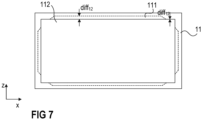
- the reduced pull-back or no pull-back sections are implemented by decreasing the distance d2 between the outer edge 113 of the dielectric insulation layer and the outer edge 1123 of the second metallization layer 112. That is, the second metallization layer 112 comprises bulges or projections in the areas of the second sections B. It is, however, generally also possible to instead increase the distance d1 between the outer edge 113 of the dielectric insulation layer 11 and the outer edge 1113 of the first metallization layer 111, as is schematically illustrated in Figure 7 . That is, the first metallization layer 111 (as outlined in a dashed line in the bottom view of Figure 7 ) may comprise dents or indentations in the areas of the second sections B.
Landscapes
- Engineering & Computer Science (AREA)
- Microelectronics & Electronic Packaging (AREA)
- Structure Of Printed Boards (AREA)
- Physics & Mathematics (AREA)
- Geometry (AREA)
Abstract
Description
- The instant disclosure relates to a substrate, in particular to a substrate for a power semiconductor module arrangement.
- Power semiconductor module arrangements often include at least one substrate arranged in a housing. A semiconductor arrangement including a plurality of controllable semiconductor elements (e.g., IGBTs, MOSFETs, HEMTs, etc.) may be arranged on each of the at least one substrate. Each substrate usually comprises a substrate layer (e.g., a ceramic layer), a first metallization layer deposited on a first side of the substrate layer, and a second metallization layer deposited on a second side of the substrate layer. The controllable semiconductor elements are mounted, for example, on the first metallization layer. The second metallization layer may be attached to a base plate. The size of the first metallization layer may be as large as possible in order to provide a large mounting surface for the semiconductor bodies and any other devices of the power semiconductor module arrangement. The size of the second metallization layer on the other hand may be chosen to be smaller than the size of the first metallization layer in order to reduce a size of the solder area when mounting the substrate to a base plate (or a heat sink), thereby reducing the risk of solder leak and/or solder splash. Similarly, it may however also be possible that the size of the second metallization layer is larger than the size of the first metallization layer for any other reasons. When a distance between the edge of the substrate layer and the edge of the second metallization layer is larger (or smaller) than a distance between the edge of the substrate layer and the edge of the first metallization layer, this is usually referred to as "pull-back". Such a pull-back, however, may increase the risk of cracks forming in the first and/or second metallization layer, especially when the metallization layers are heated to temperatures above defined threshold temperatures.
- There is a need for a substrate that offers the advantages of a pull-back design while, at the same time, having a decreased risk of cracks forming in the first and/or second metallization layers.
- A substrate includes a dielectric insulation layer, a first metallization layer arranged on a first surface of the dielectric insulation layer, and a second metallization layer arranged on a second surface of the dielectric insulation layer, opposite the first surface. The dielectric insulation layer comprises an outer edge extending between the first surface and the second surface, wherein the outer edge of the dielectric insulation layer comprises a plurality of first sections and a plurality of second sections. Along each of the plurality of first sections, a difference between a first distance and a second distance has a first value, and along each of the plurality of second sections, the difference between the first distance and the second distance has a second value that is different from the first value, wherein the first distance is a distance between the outer edge of the dielectric insulation layer and an outer edge of the first metallization layer, and the second distance is a distance between the outer edge of the dielectric insulation layer and an outer edge of the second metallization layer.
- The invention may be better understood with reference to the following drawings and the description. The components in the figures are not necessarily to scale, emphasis instead being placed upon illustrating the principles of the invention. Moreover, in the figures, like referenced numerals designate corresponding parts throughout the different views.
-
-
Figure 1 is a cross-sectional view of a power semiconductor module arrangement. -
Figure 2 , includingFigures 2A and 2B , schematically illustrates different cross-sectional views of a substrate. -
Figure 3 is a top view of a substrate according to embodiments of the disclosure. -
Figure 4 is a bottom view of a substrate according to further embodiments of the disclosure. -
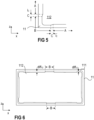
Figure 5 schematically illustrates a top view of one corner of a substrate according to embodiments of the disclosure. -
Figure 6 is a bottom view of a substrate according to further embodiments of the disclosure. -
Figure 7 is a bottom view of a substrate according to even further embodiment of the disclosure. - In the following detailed description, reference is made to the accompanying drawings. The drawings show specific examples in which the invention may be practiced. It is to be understood that the features and principles described with respect to the various examples may be combined with each other, unless specifically noted otherwise. In the description, as well as in the claims, designations of certain elements as "first element", "second element", "third element" etc. are not to be understood as enumerative. Instead, such designations serve solely to address different "elements". That is, e.g., the existence of a "third element" does not require the existence of a "first element" and a "second element". An electrical line or electrical connection as described herein may be a single electrically conductive element, or include at least two individual electrically conductive elements connected in series and/or parallel. Electrical lines and electrical connections may include metal and/or semiconductor material, and may be permanently electrically conductive (i.e., non-switchable). A semiconductor body as described herein may be made from (doped) semiconductor material and may be a semiconductor chip or be included in a semiconductor chip. A semiconductor body has electrically connecting pads and includes at least one semiconductor element with electrodes.
- Referring to
Figure 1 , a cross-sectional view of a powersemiconductor module arrangement 100 is schematically illustrated. The powersemiconductor module arrangement 100 includes a housing 7 and asubstrate 10. Thesubstrate 10 includes adielectric insulation layer 11, a (structured)first metallization layer 111 attached to thedielectric insulation layer 11, and a (structured)second metallization layer 112 attached to thedielectric insulation layer 11. Thedielectric insulation layer 11 is disposed between the first andsecond metallization layers - Each of the first and
second metallization layers substrate 10 may be a ceramic substrate, that is, a substrate in which thedielectric insulation layer 11 is a ceramic, e.g., a thin ceramic layer. The ceramic may consist of or include one of the following materials: aluminum oxide; aluminum nitride; zirconium oxide; silicon nitride; boron nitride; or any other dielectric ceramic. For example, thedielectric insulation layer 11 may consist of or include one of the following materials: Al2O3, AlN, SiC, BeO or Si3N4. For instance, thesubstrate 10 may, e.g., be a Direct Copper Bonding (DCB) substrate, a Direct Aluminum Bonding (DAB) substrate, or an Active Metal Brazing (AMB) substrate. Thesubstrate 10 may also be a conventional printed circuit board (PCB) having a non-ceramicdielectric insulation layer 11. For instance, a non-ceramicdielectric insulation layer 11 may consist of or include a cured resin. - The
substrate 10 is arranged in a housing 7. In the example illustrated inFigure 1 , thesubstrate 10 is arranged on abase plate 12 which forms a ground surface of the housing 7, while the housing 7 itself solely comprises sidewalls and a cover. This, however, is only an example. It is also possible that the housing 7 further comprises a ground surface and thesubstrate 10 and thebase plate 12 be arranged inside the housing 7. In some powersemiconductor module arrangements 100, more than onesubstrate 10 is arranged on asingle base plate 12 or on the ground surface of a housing 7. It is also possible that thesubstrate 10 itself forms a ground surface of the housing 7. - One or
more semiconductor bodies 20 may be arranged on the at least onesubstrate 10. Each of thesemiconductor bodies 20 arranged on the at least onesubstrate 10 may include a diode, an IGBT (Insulated-Gate Bipolar Transistor), a MOSFET (Metal-Oxide-Semiconductor Field-Effect Transistor), a JFET (Junction Field-Effect Transistor), a HEMT (High-Electron-Mobility Transistor), and/or any other suitable semiconductor element. - The one or
more semiconductor bodies 20 may form a semiconductor arrangement on thesubstrate 10. InFigure 1 , only twosemiconductor bodies 20 are exemplarily illustrated. Thesecond metallization layer 112 of thesubstrate 10 inFigure 1 is a continuous layer. Thefirst metallization layer 111 is a structured layer in the example illustrated inFigure 1 . "Structured layer" means that thefirst metallization layer 111 is not a continuous layer, but includes recesses between different sections of the layer. Such recesses are schematically illustrated inFigure 1 . Thefirst metallization layer 111 in this example includes three different sections. This, however, is only an example. Any other number of sections is possible.Different semiconductor bodies 20 may be mounted to the same or to different sections of thefirst metallization layer 111. Different sections of thefirst metallization layer 111 may have no electrical connection or may be electrically connected to one or more other sections using electrical connection elements 3 such as, e.g., bonding wires or bonding ribbons. Electrical connections 3 may also include connection plates, conductor rails, or connection clips, for example, to name just a few examples. The one ormore semiconductor bodies 20 may be electrically and mechanically connected to thesubstrate 10 by an electricallyconductive connection layer 30. Such an electricallyconductive connection layer 30 may be a solder layer, a layer of an electrically conductive adhesive, or a layer of a sintered metal powder, e.g., a sintered silver powder, for example. According to other examples, it is also possible that thesecond metallization layer 112 is a structured layer. - The power
semiconductor module arrangement 100 illustrated inFigure 1 further includesterminal elements 4. Theterminal elements 4 are electrically connected to thefirst metallization layer 111 and provide an electrical connection between the inside and the outside of the housing 7. Theterminal elements 4 may be electrically connected to thefirst metallization layer 111 with afirst end 41, while asecond end 42 of each of theterminal elements 4 protrudes out of the housing 7. Theterminal elements 4 may be electrically contacted from the outside at their respective second ends 42. A first part of theterminal elements 4 may extend through the inside of the housing 7 in a vertical direction y. The vertical direction y is a direction perpendicular to a top surface of thesubstrate 10, wherein the top surface of thesubstrate 10 is a surface on which the at least onesemiconductor body 20 is mounted. Theterminal elements 4 illustrated inFigure 1 , however, are only examples.Terminal elements 4 may be implemented in any other way and may be arranged anywhere within the housing 7. For example, one or moreterminal elements 4 may be arranged close to or adjacent to the sidewalls of the housing 7.Terminal elements 4 could also protrude through the sidewalls of the housing 7 instead of through the cover. Thefirst end 41 of aterminal element 4 may be electrically and mechanically connected to thesubstrate 10 by an electrically conductive connection layer, for example (not explicitly illustrated inFigure 1 ). Such an electrically conductive connection layer may be a solder layer, a layer of an electrically conductive adhesive, or a layer of a sintered metal powder, e.g., a sintered silver (Ag) powder, for example. Thefirst end 41 of aterminal element 4 may also be electrically coupled to thesubstrate 10 via one or more electrical connections 3, for example. - The power
semiconductor module arrangement 100 may further include anencapsulant 5. Anencapsulant 5 may consist of or include a silicone gel or may be a rigid molding compound, for example. Theencapsulant 5 may at least partly fill the interior of the housing 7, thereby covering the components and electrical connections that are arranged on thesubstrate 10. Theterminal elements 4 may be partly embedded in theencapsulant 5. At least their second ends 42, however, are not covered by theencapsulant 5 and protrude from theencapsulant 5 through the housing 7 to the outside of the housing 7. Theencapsulant 5 is configured to protect the components and electrical connections of thepower semiconductor module 100, in particular the components arranged on thesubstrate 10 inside the housing 7, from certain environmental conditions and mechanical damage. - In the example illustrated in
Figure 1 , a size of thesecond metallization layer 112 equals a size of thefirst metallization layer 111. That is, a distance between an outer edge of thedielectric insulation layer 11 and an outer edge of thefirst metallization layer 111 equals a distance between the outer edge of thedielectric insulation layer 11 and an outer edge of thesecond metallization layer 112 along the entire circumference of thedielectric insulation layer 11. Or, in other words, the outer edge of thefirst metallization layer 111 is aligned with the outer edge of thesecond metallization layer 112, as is emphasized by the dashed lines inFigure 1 . - Usually, the size of the
first metallization layer 111 is as large as possible in order to provide a large mounting surface for thesemiconductor bodies 20 and any other devices (e.g., terminal elements 4) of the power semiconductor module arrangement. The size of thesecond metallization layer 112 on the other hand may be chosen to be smaller than the size of thefirst metallization layer 111 in order to reduce a size of the solder area when mounting thesubstrate 10 to abase plate 12, thereby reducing the risk of solder leak and/or solder splash. That is, the distance d1 between theouter edge 113 of thedielectric insulation layer 11 and theouter edge 1113 of thefirst metallization layer 111 may be less than the distance d2 between theouter edge 113 of thedielectric insulation layer 11 and theouter edge 1123 of thesecond metallization layer 112 along the entire circumference of thedielectric insulation layer 11, as is exemplarily illustrated in the cross-sectional view ofFigure 2A . Similarly, for any reasons, it may however also be possible that the size of thesecond metallization layer 112 is larger than the size of thefirst metallization layer 111 such that the distance d1 between theouter edge 113 of thedielectric insulation layer 11 and theouter edge 1113 of thefirst metallization layer 111 is greater than the distance d2 between theouter edge 113 of thedielectric insulation layer 11 and theouter edge 1123 of thesecond metallization layer 112 along the entire circumference of the dielectric insulation layer 11 (not specifically illustrated). - When a distance d2 between the
outer edge 113 of thedielectric insulation layer 11 and theouter edge 1123 of thesecond metallization layer 112 is larger (or smaller) than a distance d1 between theouter edge 113 of thedielectric insulation layer 11 and theouter edge 1113 of thefirst metallization layer 111, this is usually referred to as "pull-back". Such a pull-back, however, may increase the risk of cracks forming in the first and/or second metallization layers 111, 112, especially when the metallization layers 111, 112 are heated to temperatures above defined threshold temperatures. This is, because the pull-back may result in high tensions in thedielectric insulation layer 11. Such tensions may be further influenced by a temperature of thesubstrate 10 due to the so-called bi-metallic effect (increased tension at higher temperatures). - Now referring to
Figure 2 , different cross-sectional views of asubstrate 10 according to embodiments of the disclosure are schematically illustrated. Thesubstrate 10 comprises adielectric insulation layer 11, afirst metallization layer 111 arranged on afirst surface 101 of thedielectric insulation layer 11, and asecond metallization layer 112 arranged on asecond surface 102 of thedielectric insulation layer 11, opposite thefirst surface 101. Thedielectric insulation layer 11 comprises anouter edge 113 extending between thefirst surface 101 and thesecond surface 102, wherein theouter edge 113 of thedielectric insulation layer 11 comprises a plurality of first sections A and a plurality of second sections B (see, e.g., top view of substrate illustrated inFigure 3 ). Along each of the plurality of first sections A, a difference diff12 between a first distance d1 and a second distance d2 has a first value v, and along each of the plurality of second sections B, the difference diff12 between the first distance d1 and the second distance d2 has a second value w that is different from the first value (v ≠ w). The first distance d1 is a distance between theouter edge 113 of thedielectric insulation layer 11 and anouter edge 1113 of thefirst metallization layer 111, and the second distance d2 is a distance between theouter edge 113 of thedielectric insulation layer 11 and anouter edge 1123 of thesecond metallization layer 112. - That is, along the first sections A

sections B 
According to one embodiment of the disclosure, the following may apply: v > w (first value v greater than second value w). - The first sections A may be referred to as pull-back sections or full pull-back sections, and the second sections B may be referred to as no pull-back sections or reduced pull-back sections, for example. By providing sections with a full pull-back as well as sections with a reduced or even no pull-back, the advantages of the pull-back design are combined with the advantages of a no-pullback design or at least a reduced pull-back design. That is, in the second sections B, the tensions arising in the
dielectric insulation layer 11 may be significantly reduced while still providing the advantages of the pull-back design along the first sections A. Top and bottom views ofsubstrates 10 according to embodiments of the disclosure are schematically illustrated inFigures 3 (no pull-back design in second sections B) and 4 (reduced pull-back design in second sections B).Figure 3 schematically illustrates a top view in which thefirst metallization layer 111 is visible, while the second metallization layer 112 (illustrated in dashed lines) is concealed by thefirst metallization layer 111 and thedielectric insulation layer 11.Figure 4 schematically illustrates a bottom view of asubstrate 10 in which thesecond metallization layer 112 is visible, while the first metallization layer 111 (illustrated in dashed lines) is concealed by thesecond metallization layer 112 and thedielectric insulation layer 11.Figure 2A schematically illustrates a cross-sectional view along a section line D - D', andFigure 2B schematically illustrates a cross-sectional view along a section line E - E' of thesubstrate 10 as illustrated inFigure 4 . - As can be seen in
Figures 3 and 4 , for example, the first sections A and the second sections B are arranged alternatingly along the circumference of thedielectric insulation layer 11. Thesubstrate 10 may comprise at least two first sections A and at least two second sections B, for example. The number of first sections A generally equals the number of second sections B. Thedielectric insulation layer 11 may have a rectangular shape, and each of the second sections B may be arranged at a different corner of thedielectric insulation layer 11, for example, as is schematically illustrated inFigures 3 and 4 . This, however, is only an example. Alternatively or additionally, second sections B may also be arranged anywhere along the sides of thedielectric insulation layer 11, as is schematically illustrated inFigure 6 . A length of a second section B extending along a side of thedielectric insulation layer 11, however, is less than the length of the respective side of thedielectric insulation layer 11. For example, a length of a second section B extending along a side of thedielectric insulation layer 11 may be less than 50% or even less than 30% of the respective side of thedielectric insulation layer 11. - The
substrate 10 illustrated inFigure 6 comprises one additional second section B along each of the longitudinal sides of the dielectric insulation layer 11 (a rectangulardielectric insulation layer 11 generally comprises two longitudinal sides extending in parallel to each other, and two narrow sides extending in parallel to each other and perpendicular to the longitudinal sides). Additionally or alternatively, second sections B may be arranged anywhere along the circumference of thedielectric insulation layer 11. It is also possible that two or more second sections B are arranged along one side of thedielectric insulation layer 11. Generally, second sections B with a reduced pull-back or no pull-back may be arranged in those sections along the circumference of thedielectric insulation layer 11 that are particularly sensitive and prone to cracks forming in the first and/or second metallization layers 111, 112. - The corners of the metallization layers 111, 112, for example, may be particularly sensitive and prone to the formation of cracks in a pull-back design. With the second sections B extending along the corners of the
dielectric insulation layer 11, as illustrated inFigures 3 and 4 , the formation of cracks in the area of the corners of the metallization layers 111, 112 may be significantly reduced or even entirely avoided. Each of the second sections B may extend from the respective corner in a first horizontal direction x and in a second horizontal direction z that is perpendicular to the first horizontal direction x (see, e.g.,Figure 4 ). According to one embodiment of the disclosure, a length lBx of each of the second sections B in the first horizontal direction x may be less than 15mm (Millimeters), and a length lBz of each of the second sections B in the second horizontal direction z is less than 15mm. According to another embodiment of the disclosure, the length lBx of each of the second sections B in the first horizontal direction x may be less than 5mm, and the length lBz of each of the second sections B in the second horizontal direction z may be less than 5mm. According to an even further embodiment of the disclosure, the length lBx of each of the second sections B in the first horizontal direction x may be less than 3mm, and the length lBz of each of the second sections B in the second horizontal direction z may be less than 3mm. The length lBx of each of the second sections B in the first horizontal direction x may equal the length lBz of each of the second sections B in the second horizontal direction z. It is, however, also possible that the length lBx of a second section B in the first horizontal direction x differs from the length lBz of the respective second sections B in the second horizontal direction z. - The first value v may be between 0.2mm and 1.2mm (millimeters), for example. That is, 0.2mm ≤ v ≤ 1.2mm, for example. The second value w may be 50% of the first value v, or less. That is, w ≤ 0.5 * v, for example. When w = 0.5 * v, the pull-back is already significantly decreased, thereby also decreasing the tension along the second sections B. By further reducing the pull-back (e.g., 0 < w < 0.5 * v), the tension may be decreased even further. If w = 0, the respective second section B is a no pull-back section, and the tension may be reduced to a minimum. A no-pull back region, however, generally does not profit from the advantages of a pull-back at all. Whether the second sections B are implemented as reduced pull-back sections or no pull-back sections generally depends on the overall design of the power semiconductor module arrangement and the application it is used for. In some cases, reduced pull-back sections may be preferable, while in other cases no pull-back sections may be more appropriate.
- Now referring to
Figure 5 , thedielectric insulation layer 11 may further comprise a plurality of third sections C, wherein each third section C is arranged between a first section A and a second section B. Along each of the third sections C, the difference diff12 gradually transitions from the first value v to the second value w. That is, a transition between the first sections A and the second sections B may be comparably smooth. A length lc of a third section C (distance between first section A and second section B) may be between 0.1 and 5mm (millimeters), for example. It is, however, also possible that the third sections C be omitted. That is, there may be a hard edge between the first sections A and the second sections B. A smooth transition between the first sections A and the second sections B by means of the third sections C, however, may further decrease the tension in thedielectric insulation layer 11. - In the examples illustrated in
Figures 3 to 6 , the reduced pull-back or no pull-back sections (second sections) are implemented by decreasing the distance d2 between theouter edge 113 of the dielectric insulation layer and theouter edge 1123 of thesecond metallization layer 112. That is, thesecond metallization layer 112 comprises bulges or projections in the areas of the second sections B. It is, however, generally also possible to instead increase the distance d1 between theouter edge 113 of thedielectric insulation layer 11 and theouter edge 1113 of thefirst metallization layer 111, as is schematically illustrated inFigure 7 . That is, the first metallization layer 111 (as outlined in a dashed line in the bottom view ofFigure 7 ) may comprise dents or indentations in the areas of the second sections B.
Claims (14)
- A substrate (10) comprises,a dielectric insulation layer (11);a first metallization layer (111) arranged on a first surface (101) of the dielectric insulation layer (11); anda second metallization layer (112) arranged on a second surface (102) of the dielectric insulation layer (11), opposite the first surface (101),wherein the dielectric insulation layer (11) comprises an outer edge (113) extending between the first surface (101) and the second surface (102), wherein the outer edge (113) of the dielectric insulation layer (11) comprises a plurality of first sections (A) and a plurality of second sections (B),wherein along each of the plurality of first sections (A), a difference (diff12) between a first distance (d1) and a second distance (d2) has a first value (v),wherein along each of the plurality of second sections (B), the difference (diff12) between the first distance (d1) and the second distance (d2) has a second value (w) that is different from the first value (v), andwherein the first distance (d1) is a distance between the outer edge (113) of the dielectric insulation layer (11) and an outer edge (1113) of the first metallization layer (111), and the second distance (d2) is a distance between the outer edge (113) of the dielectric insulation layer (11) and an outer edge (1123) of the second metallization layer (112).
- The substrate (10) of claim 1, wherein the first sections (A) and the second sections (B) are arranged alternatingly along the circumference of the dielectric insulation layer (11).
- The substrate (10) of claim 1 or 2, wherein the dielectric insulation layer (11) has a rectangular shape, and each of the second sections (B) is arranged at a different corner of the dielectric insulation layer (11).
- The substrate (10) of claim 3, wherein each of the second sections (B) extends from the respective corner in a first horizontal direction (x) and in a second horizontal direction (z) that is perpendicular to the first horizontal direction (x).
- The substrate (10) of claim 4, whereina length (lBx) of each of the second sections (B) in the first horizontal direction (x) is less than 15mm, anda length (lBz) of each of the second sections (B) in the second horizontal direction (z) is less than 15mm.
- The substrate (10) of claim 5, whereinthe length (lBx) of each of the second sections (B) in the first horizontal direction (x) is less than 5mm, andthe length (lBz) of each of the second sections (B) in the second horizontal direction (z) is less than 5mm.
- The substrate (10) of claim 6, whereinthe length (lBx) of each of the second sections (B) in the first horizontal direction (x) is less than 3mm, andthe length (lBz) of each of the second sections (B) in the second horizontal direction (z) is less than 3mm.
- The substrate (10) of any of claims 5 to 7, wherein the length (lBx) of each of the second sections (B) in the first horizontal direction (x) equals the length (lBz) of each of the second sections (B) in the second horizontal direction (z).
- The substrate (10) of any of the preceding claims, wherein the first value (v) is between 0.2mm and 1.2mm.
- The substrate (10) of any of the preceding claims, wherein the first value (v) is greater than the second value (w).
- The substrate (10) of claim 10, wherein the second value (w) is 50% of the first value (v) or less.
- The substrate (10) of claim 11, wherein the second value (w) is zero.
- The substrate (10) of any of the preceding claims, wherein the dielectric insulation layer (11) further comprises a plurality of third sections (C), wherein each third section (C) is arranged between a first section (A) and a second section (B), and wherein along each of the third sections (C), the difference (diff12) gradually transitions from the first value (v) to the second value (w).
- The substrate (10) of claim 13, wherein a length (lc) of each of the third sections (C) is between 0.1mm and 5mm.
Priority Applications (3)
| Application Number | Priority Date | Filing Date | Title |
|---|---|---|---|
| EP23158108.3A EP4422358A1 (en) | 2023-02-23 | 2023-02-23 | Substrate |
| US18/442,135 US20240290707A1 (en) | 2023-02-23 | 2024-02-15 | Substrate |
| CN202410195286.7A CN118538702A (en) | 2023-02-23 | 2024-02-22 | Substrate |
Applications Claiming Priority (1)
| Application Number | Priority Date | Filing Date | Title |
|---|---|---|---|
| EP23158108.3A EP4422358A1 (en) | 2023-02-23 | 2023-02-23 | Substrate |
Publications (1)
| Publication Number | Publication Date |
|---|---|
| EP4422358A1 true EP4422358A1 (en) | 2024-08-28 |
Family
ID=85381491
Family Applications (1)
| Application Number | Title | Priority Date | Filing Date |
|---|---|---|---|
| EP23158108.3A Pending EP4422358A1 (en) | 2023-02-23 | 2023-02-23 | Substrate |
Country Status (3)
| Country | Link |
|---|---|
| US (1) | US20240290707A1 (en) |
| EP (1) | EP4422358A1 (en) |
| CN (1) | CN118538702A (en) |
Citations (2)
| Publication number | Priority date | Publication date | Assignee | Title |
|---|---|---|---|---|
| DE4004844C1 (en) * | 1990-02-16 | 1991-01-03 | Abb Ixys Semiconductor Gmbh | Copper metallisation on ceramic substrate - obtd. by bonding copper foil directly to whole surface of substrate, then masking and etching |
| US5403651A (en) * | 1991-10-14 | 1995-04-04 | Fuji Electric Co., Ltd. | Insulating substrate for mounting semiconductor devices |
-
2023
- 2023-02-23 EP EP23158108.3A patent/EP4422358A1/en active Pending
-
2024
- 2024-02-15 US US18/442,135 patent/US20240290707A1/en active Pending
- 2024-02-22 CN CN202410195286.7A patent/CN118538702A/en active Pending
Patent Citations (2)
| Publication number | Priority date | Publication date | Assignee | Title |
|---|---|---|---|---|
| DE4004844C1 (en) * | 1990-02-16 | 1991-01-03 | Abb Ixys Semiconductor Gmbh | Copper metallisation on ceramic substrate - obtd. by bonding copper foil directly to whole surface of substrate, then masking and etching |
| US5403651A (en) * | 1991-10-14 | 1995-04-04 | Fuji Electric Co., Ltd. | Insulating substrate for mounting semiconductor devices |
Also Published As
| Publication number | Publication date |
|---|---|
| CN118538702A (en) | 2024-08-23 |
| US20240290707A1 (en) | 2024-08-29 |
Similar Documents
| Publication | Publication Date | Title |
|---|---|---|
| US11942449B2 (en) | Semiconductor arrangement and method for producing the same | |
| US11699625B2 (en) | Power semiconductor module arrangement | |
| CN113228265B (en) | Circuit structure of semiconductor components | |
| US12387987B2 (en) | Housing, semiconductor module comprising a housing and method for producing a housing | |
| EP4084062A1 (en) | Power semiconductor module arrangement | |
| US11282774B2 (en) | Power semiconductor module arrangement | |
| EP4071793A1 (en) | Power semiconductor module arrangement and housing for a power semiconductor module arrangement | |
| US20240290707A1 (en) | Substrate | |
| US20230170286A1 (en) | Terminal Element or Bus Bar, and Power Semiconductor Module Arrangement Comprising a Terminal Element or Bus Bar | |
| EP3696851A1 (en) | Semiconductor arrangement and method for producing the same | |
| EP4428914A1 (en) | Power semiconductor module arrangement | |
| EP4607584A1 (en) | Semiconductor module arrangement | |
| EP4439649A1 (en) | Substrate arrangement | |
| EP4113605B1 (en) | Power semiconductor module arrangement | |
| EP4421868A1 (en) | Semiconductor module arrangement | |
| US20260047494A1 (en) | Semiconductor module arrangement | |
| EP4220704A1 (en) | Printed circuit board, power semiconductor module arrangement comprising a printed circuit board, and method for assembling the same | |
| EP4601000A1 (en) | Power semiconductor module arrangement and method for producing the same | |
| EP4270466A1 (en) | Power semiconductor module arrangements and methods for producing power semiconductor module arrangements | |
| EP4700827A1 (en) | Power semiconductor module arrangement | |
| US20260053056A1 (en) | Housing and semiconductor module having a housing | |
| EP4510184A1 (en) | Terminal element, and power semiconductor module arrangement comprising a terminal element | |
| EP4345884A1 (en) | Power semiconductor module arrangement and printed circuit board for a power semiconductor module arrangement | |
| US20250226286A1 (en) | Heat dissipation base, semiconductor module, and energy conversion device |
Legal Events
| Date | Code | Title | Description |
|---|---|---|---|
| PUAI | Public reference made under article 153(3) epc to a published international application that has entered the european phase |
Free format text: ORIGINAL CODE: 0009012 |
|
| STAA | Information on the status of an ep patent application or granted ep patent |
Free format text: STATUS: REQUEST FOR EXAMINATION WAS MADE |
|
| 17P | Request for examination filed |
Effective date: 20240228 |
|
| AK | Designated contracting states |
Kind code of ref document: A1 Designated state(s): AL AT BE BG CH CY CZ DE DK EE ES FI FR GB GR HR HU IE IS IT LI LT LU LV MC ME MK MT NL NO PL PT RO RS SE SI SK SM TR |
|
| GRAP | Despatch of communication of intention to grant a patent |
Free format text: ORIGINAL CODE: EPIDOSNIGR1 |
|
| STAA | Information on the status of an ep patent application or granted ep patent |
Free format text: STATUS: GRANT OF PATENT IS INTENDED |
|
| RIC1 | Information provided on ipc code assigned before grant |
Ipc: H05K 1/02 20060101AFI20260407BHEP Ipc: H10W 40/25 20260101ALI20260407BHEP Ipc: H05K 1/03 20060101ALN20260407BHEP |