EP4421874A1 - High performance silicon controlled rectifier devices - Google Patents
High performance silicon controlled rectifier devices Download PDFInfo
- Publication number
- EP4421874A1 EP4421874A1 EP24152507.0A EP24152507A EP4421874A1 EP 4421874 A1 EP4421874 A1 EP 4421874A1 EP 24152507 A EP24152507 A EP 24152507A EP 4421874 A1 EP4421874 A1 EP 4421874A1
- Authority
- EP
- European Patent Office
- Prior art keywords
- well
- semiconductor material
- porous semiconductor
- porous
- semiconductor substrate
- Prior art date
- Legal status (The legal status is an assumption and is not a legal conclusion. Google has not performed a legal analysis and makes no representation as to the accuracy of the status listed.)
- Pending
Links
Images



Classifications
-
- H—ELECTRICITY
- H10—SEMICONDUCTOR DEVICES; ELECTRIC SOLID-STATE DEVICES NOT OTHERWISE PROVIDED FOR
- H10D—INORGANIC ELECTRIC SEMICONDUCTOR DEVICES
- H10D89/00—Aspects of integrated devices not covered by groups H10D84/00 - H10D88/00
- H10D89/60—Integrated devices comprising arrangements for electrical or thermal protection, e.g. protection circuits against electrostatic discharge [ESD]
- H10D89/601—Integrated devices comprising arrangements for electrical or thermal protection, e.g. protection circuits against electrostatic discharge [ESD] for devices having insulated gate electrodes, e.g. for IGFETs or IGBTs
- H10D89/711—Integrated devices comprising arrangements for electrical or thermal protection, e.g. protection circuits against electrostatic discharge [ESD] for devices having insulated gate electrodes, e.g. for IGFETs or IGBTs using bipolar transistors as protective elements
- H10D89/713—Integrated devices comprising arrangements for electrical or thermal protection, e.g. protection circuits against electrostatic discharge [ESD] for devices having insulated gate electrodes, e.g. for IGFETs or IGBTs using bipolar transistors as protective elements including a PNP transistor and a NPN transistor, wherein each of said transistors has its base region coupled to the collector region of the other transistor, e.g. silicon controlled rectifier [SCR] devices
-
- H—ELECTRICITY
- H10—SEMICONDUCTOR DEVICES; ELECTRIC SOLID-STATE DEVICES NOT OTHERWISE PROVIDED FOR
- H10D—INORGANIC ELECTRIC SEMICONDUCTOR DEVICES
- H10D8/00—Diodes
- H10D8/80—PNPN diodes, e.g. Shockley diodes or break-over diodes
-
- H—ELECTRICITY
- H10—SEMICONDUCTOR DEVICES; ELECTRIC SOLID-STATE DEVICES NOT OTHERWISE PROVIDED FOR
- H10D—INORGANIC ELECTRIC SEMICONDUCTOR DEVICES
- H10D18/00—Thyristors
-
- H—ELECTRICITY
- H10—SEMICONDUCTOR DEVICES; ELECTRIC SOLID-STATE DEVICES NOT OTHERWISE PROVIDED FOR
- H10D—INORGANIC ELECTRIC SEMICONDUCTOR DEVICES
- H10D18/00—Thyristors
- H10D18/01—Manufacture or treatment
-
- H—ELECTRICITY
- H10—SEMICONDUCTOR DEVICES; ELECTRIC SOLID-STATE DEVICES NOT OTHERWISE PROVIDED FOR
- H10D—INORGANIC ELECTRIC SEMICONDUCTOR DEVICES
- H10D62/00—Semiconductor bodies, or regions thereof, of devices having potential barriers
- H10D62/10—Shapes, relative sizes or dispositions of the regions of the semiconductor bodies; Shapes of the semiconductor bodies
- H10D62/113—Isolations within a component, i.e. internal isolations
- H10D62/115—Dielectric isolations, e.g. air gaps
-
- H—ELECTRICITY
- H10—SEMICONDUCTOR DEVICES; ELECTRIC SOLID-STATE DEVICES NOT OTHERWISE PROVIDED FOR
- H10D—INORGANIC ELECTRIC SEMICONDUCTOR DEVICES
- H10D62/00—Semiconductor bodies, or regions thereof, of devices having potential barriers
- H10D62/10—Shapes, relative sizes or dispositions of the regions of the semiconductor bodies; Shapes of the semiconductor bodies
- H10D62/124—Shapes, relative sizes or dispositions of the regions of semiconductor bodies or of junctions between the regions
-
- H—ELECTRICITY
- H10—SEMICONDUCTOR DEVICES; ELECTRIC SOLID-STATE DEVICES NOT OTHERWISE PROVIDED FOR
- H10D—INORGANIC ELECTRIC SEMICONDUCTOR DEVICES
- H10D62/00—Semiconductor bodies, or regions thereof, of devices having potential barriers
- H10D62/40—Crystalline structures
- H10D62/402—Amorphous materials
-
- H—ELECTRICITY
- H10—SEMICONDUCTOR DEVICES; ELECTRIC SOLID-STATE DEVICES NOT OTHERWISE PROVIDED FOR
- H10D—INORGANIC ELECTRIC SEMICONDUCTOR DEVICES
- H10D62/00—Semiconductor bodies, or regions thereof, of devices having potential barriers
- H10D62/80—Semiconductor bodies, or regions thereof, of devices having potential barriers characterised by the materials
- H10D62/83—Semiconductor bodies, or regions thereof, of devices having potential barriers characterised by the materials being Group IV materials, e.g. B-doped Si or undoped Ge
-
- H—ELECTRICITY
- H10—SEMICONDUCTOR DEVICES; ELECTRIC SOLID-STATE DEVICES NOT OTHERWISE PROVIDED FOR
- H10D—INORGANIC ELECTRIC SEMICONDUCTOR DEVICES
- H10D8/00—Diodes
- H10D8/01—Manufacture or treatment
- H10D8/041—Manufacture or treatment of multilayer diodes
-
- H—ELECTRICITY
- H10—SEMICONDUCTOR DEVICES; ELECTRIC SOLID-STATE DEVICES NOT OTHERWISE PROVIDED FOR
- H10D—INORGANIC ELECTRIC SEMICONDUCTOR DEVICES
- H10D84/00—Integrated devices formed in or on semiconductor substrates that comprise only semiconducting layers, e.g. on Si wafers or on GaAs-on-Si wafers
- H10D84/01—Manufacture or treatment
- H10D84/0112—Integrating together multiple components covered by H10D8/00, H10D10/00 or H10D18/00, e.g. integrating multiple BJTs
-
- H—ELECTRICITY
- H10—SEMICONDUCTOR DEVICES; ELECTRIC SOLID-STATE DEVICES NOT OTHERWISE PROVIDED FOR
- H10D—INORGANIC ELECTRIC SEMICONDUCTOR DEVICES
- H10D84/00—Integrated devices formed in or on semiconductor substrates that comprise only semiconducting layers, e.g. on Si wafers or on GaAs-on-Si wafers
- H10D84/01—Manufacture or treatment
- H10D84/02—Manufacture or treatment characterised by using material-based technologies
- H10D84/03—Manufacture or treatment characterised by using material-based technologies using Group IV technology, e.g. silicon technology or silicon-carbide [SiC] technology
- H10D84/038—Manufacture or treatment characterised by using material-based technologies using Group IV technology, e.g. silicon technology or silicon-carbide [SiC] technology using silicon technology, e.g. SiGe
Definitions
- the present disclosure relates to semiconductor structures and, more particularly, to high performance silicon controlled rectifier (SCR) devices and methods of manufacture.
- SCR silicon controlled rectifier
- a silicon controlled rectifier is a solid-state current-controlling device, which is a unidirectional device (i.e., can conduct current only in one direction).
- the SCR typically includes a switching configuration comprising p-n-p-n layers.
- a holding current of an SCR can be defined as the smallest amount of current under which an anode current has to drop to enter an OFF status. This means if the holding current value is 5 mA, for example, subsequently the SCR's anodes' current has to turn into less than 5 mA to discontinue performing.
- a triggering voltage may occur when the anode terminal is made +ve relating to the cathode in which case the SCR will be in a forwarding biased mode, e.g., enters into the forward blocking state. This means the device is switched from the blocked (OFF) state to the unblocked (ON) state.
- a structure comprises: a first well in a semiconductor substrate; a second well in the semiconductor substrate, adjacent to the first well; and a porous semiconductor region extending in the first well and the second well.
- a structure comprises: a p-well in a semiconductor substrate; a n-well in the semiconductor substrate and abutting the p-well; first diffusion regions in the n-well connecting to an anode; second diffusion regions in the p-well and connecting to a cathode; shallow trench isolation structures extending into the n-well and the p-well and isolating the first diffusion regions and the second diffusion regions; and a porous semiconductor material at junction of the n-well and the p-well.
- a method comprises: forming a first well in a semiconductor substrate; forming a second well in the semiconductor substrate, adjacent to the first well; and forming a porous semiconductor region extending in the first well and the second well.
- the present disclosure relates to semiconductor structures and, more particularly, to high performance silicon controlled rectifier (SCR) devices and methods of manufacture.
- the SCR devices include a porous semiconductor material, e.g., silicon, which sits on an N-well/P-well junction.
- the SCR devices are high holding SCR devices which also exhibit a lower trigger voltage compared to conventional SCR devices.
- the high current performance is due to a deeper current path.
- the use of porous semiconductor material effectively provides a smaller footprint compared to conventional SCR devices.
- the SCR device includes a first terminal in a first well and a second terminal in a second well adjacent to the first well.
- the first well abuts the second well along an interface or junction.
- a porous semiconductor region is provided at the junction of the first well and the second well. In this way, the interface or junction is at least partially within the porous semiconductor region.
- the SCR device further comprises a shallow trench isolation structure between the first terminal and the second terminal, with the porous semiconductor structure underneath the shallow trench isolation structure.
- the shallow trench isolation structure may be provided within the porous semiconductor region.
- the SCR devices of the present disclosure can be manufactured in a number of ways using a number of different tools.
- the methodologies and tools are used to form structures with dimensions in the micrometer and nanometer scale.
- the methodologies, i.e., technologies, employed to manufacture the SCR devices of the present disclosure have been adopted from integrated circuit (IC) technology.
- the structures are built on wafers and are realized in films of material patterned by photolithographic processes on the top of a wafer.
- the fabrication of the SCR devices uses three basic building blocks: (i) deposition of thin films of material on a substrate, (ii) applying a patterned mask on top of the films by photolithographic imaging, and (iii) etching the films selectively to the mask.
- precleaning processes may be used to clean etched surfaces of any contaminants, as is known in the art.
- rapid thermal anneal processes may be used to drive-in dopants or material layers as is known in the art.
- FIG. 1 shows a SCR device with porous semiconductor material and respective fabrication processes in accordance with aspects of the present disclosure.
- the structure 10 of FIG. 1 includes a semiconductor substrate 12 composed of any suitable material including, but not limited to, Si, SiGe, SiGeC, SiC, GaAs, InAs, InP, and other III/V or II/VI compound semiconductors.
- the semiconductor substrate 12 may be a lightly doped p-type semiconductor substrate.
- the semiconductor substrate 12 may be a lightly doped p-type, single crystalline Si substrate with any suitable crystallographic orientation (e.g., a (100), (110), (111), or (001) crystallographic orientation).
- the semiconductor substrate 12 may include wells 14, 16.
- the well 14 may be an N-well and the well 16 may be a P-well.
- the wells 14, 16 are abutting.
- the wells 14, 16 may be formed by introducing different dopant types into the semiconductor substrate 12 by, for example, ion implantation processes.
- a porous semiconductor material 18 may be provided at the interface or junction of the wells 14, 16.
- the porous semiconductor material 18 may extend laterally into both the wells 14, 16, below a top surface of the semiconductor substrate 12.
- the porous semiconductor material 18 may be porous silicon; although other semiconductor materials are also contemplated herein.
- the depth of the porous semiconductor material 18 may be adjusted to different depths at the interface or junction of the wells 14, 16, depending on required device characteristics and growth processes, as examples.
- the porous semiconductor material 18 may be comprised of a porous semiconductor material having an electrical resistivity that is greater than the electrical resistivity of the semiconductor material of the semiconductor substrate 12.
- the porous semiconductor material 18 may have an electrical resistivity that is greater than 1000 ohm-cm.
- the porous semiconductor material 18 may have a porosity characterized by a pore size that may range from a few nanometers to several hundreds of nanometers.
- the porous semiconductor material 18 may be free of crystalline grains and grain boundaries characteristic of a polycrystalline semiconductor material, such as polysilicon.
- shallow trench isolation structures 20, 20a may be provided within the semiconductor substrate 12.
- the shallow trench isolation structures 20, 20a extend vertically into the wells 14, 16 and isolate diffusion regions 22, 24.
- the diffusion regions 22 are N+ diffusion regions and the diffusion regions 24 are P+ diffusion regions, each of which vertically extend into the semiconductor substrate 12 and, more specifically, within the wells 14, 16.
- the shallow trench isolation structure 20a is provided over and extends to the porous semiconductor material 18 at a junction of the wells 14, 16.
- FIG. 1 also representatively shows contacts and/or wiring structures 26a to an anode 28 and contacts and/or wiring structures 26b to a cathode 30.
- the anode 28 is connected to the diffusion regions 22, 24 of the N-well 14 and the cathode 30 is connected to the diffusion regions 22, 24 of the P-well 16.
- the contacts and/or wiring structures 26a, 26b may contact silicide contacts on the diffusion regions 22, 24.
- the silicide contacts may be formed by a silicide process which begins with deposition of a thin transition metal layer, e.g., nickel, cobalt or titanium, over fully formed and patterned semiconductor devices (e.g., doped or ion implanted diffusion regions). After deposition of the material, the structure is heated allowing the transition metal to react with exposed silicon (or other semiconductor material as described herein) in the active regions of the semiconductor device (e.g., doped or ion implanted diffusion regions) forming a low-resistance transition metal silicide. Following the reaction, any remaining transition metal is removed by chemical etching, leaving silicide contacts in the active regions of the device.
- a thin transition metal layer e.g., nickel, cobalt or titanium
- semiconductor devices e.g., doped or ion implanted diffusion regions
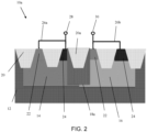
- FIG. 2 shows an SCR device with porous semiconductor material in accordance with additional aspects of the present disclosure.
- the porous semiconductor material 18a may extend to a top surface of the semiconductor substrate 12.
- the shallow trench isolation structure 20a may be provided within the porous semiconductor material 18a. In this way, the shallow trench isolation structure 20a is embedded within and surrounded by the porous semiconductor material 18a at a junction of the wells 14, 16.
- the remaining features are similar to the structure 10 of FIG. 1 .
- the porous semiconductor material will have a lower dielectric constant than the dielectric materials of the shallow trench isolation structures 20, 20a.
- the porous semiconductor material will provide a higher resistance for carriers, and will exhibit a lower capacitance.
- the porous semiconductor material will allow the current to be pushed deeper into the semiconductor substrate 12 than conventional structures, e.g., under the shallow trench isolation structure 20a, to block current and increase the high holding voltage. Also, the use of the porous semiconductor material provides a lower trigger voltage.
- FIG. 3 shows a SCR device with porous semiconductor material of FIG. 1 and a deep N-well 32 in accordance with aspects of the present disclosure.
- the deep N-well 32 is provided within the semiconductor substrate 12, which isolates the SCR device.
- the wells 14, 16 and porous material 18 sit within the deep N-well 32 and are isolated from other devices utilizing the semiconductor substrate 12. In this way, the SCR device is isolated within the semiconductor substrate 12.
- the deep N-well 32 may be formed by a conventional ion implantation process as is known in the art and described herein.
- the remaining features of the structure 10b are similar to the structure 10 of FIG. 1 .
- FIG. 4 shows a SCR device with porous semiconductor material of FIG. 2 and a deep N-well 32 in accordance with aspects of the present disclosure.
- the deep N-well 32 is provided within the semiconductor substrate 12, which isolates the SCR device.
- the wells 14, 16 and porous material 18 sit within the deep N-well 32 and are isolated from other devices utilizing the semiconductor substrate 12. In this way, the SCR device is isolated within the semiconductor substrate 12.
- the deep N-well 32 may be formed by a conventional ion implantation process as is known in the art and described herein.
- the remaining features of the structure 10b are similar to the structure 10a of FIG. 2 .
- FIGS. 5A-5C show fabrication processes for manufacturing the SCR device with porous semiconductor material of FIG. 1 .
- the porous semiconductor material 18 is formed within the semiconductor substrate 12.
- the porous semiconductor material 18 may be fabricated by, for example, electrochemical anodization or chemical etching of single-crystal semiconductor material of the semiconductor substrate 12.
- the porous semiconductor material 18, amongst the features noted with respect to FIG. 1 includes a single-crystal matrix and interconnected pores distributed within the single-crystal matrix.
- shallow trench isolation structures 20, 20a are formed within the semiconductor substrate 12.
- the shallow trench isolation structures 20, 20a may be positioned to extend within wells 14, 16 and isolate diffusion regions 22, 24 which are formed in later fabrication processes as shown in FIG. 5C .
- the shallow trench isolation structures 20, 20a can be formed by conventional lithography, etching and deposition methods known to those of skill in the art.
- a resist formed over the semiconductor substrate 12 and porous semiconductor material 18 is exposed to energy (light) and developed to form a pattern (opening).
- An etching process with a selective chemistry e.g., reactive ion etching (RIE)
- RIE reactive ion etching
- the etching process to form the trench for the shallow trench isolation structure 20a may completely remove the porous semiconductor material 18 at the upper portion of the structure.
- the etching process to form the trench for the shallow trench isolation structure 20a will partially remove the porous semiconductor material 18.
- insulator material e.g., SiO 2
- CVD chemical vapor deposition
- Any residual material on the surface of the semiconductor material 12 can be removed by conventional chemical mechanical polishing (CMP) processes.
- FIG. 5C shows the fabrication processes of forming the wells 14, 16 and diffusion regions 22, 24.
- the wells 14, 16 and diffusion regions 22, 24 may be formed by introducing a concentration of a different dopant of opposite conductivity type in the semiconductor substrate.
- the wells 14, 16 will abut one another; whereas the diffusion regions 22, 24 will be provided between the shallow trench isolation structures 20, 20a and within the wells 14, 16.
- respective patterned implantation masks may be used to define selected areas exposed for the implantations of the wells 14, 16 and diffusion regions 22, 24.
- the implantation mask used to select the exposed area for forming a well and/or fission regions is stripped after implantation, and before the implantation mask used to form another well or diffusion regions of different conductivity type.
- the implantation masks may include a layer of a light-sensitive material, such as an organic photoresist, applied by a spin coating process, pre-baked, exposed to light projected through a photomask, baked after exposure, and developed with a chemical developer.
- Each of the implantation masks has a thickness and stopping power sufficient to block masked areas against receiving a dose of the implanted ions.
- the P-well 16 and p-diffusion regions 24 may be doped with different concentrations of p-type dopants, e.g., Boron (B), and the N-well 14 and n-diffusion regions 22 may be doped with different concentrations of n-type dopants, e.g., Arsenic (As), Phosphorus (P) and Antimony (Sb), among other suitable examples.
- An annealing process may be performed to drive in the dopant into the semiconductor substrate 12.
- the contacts and/or wiring structures 26a, 26b may be formed by conventional back end of the line (BEOL) processes.
- BEOL back end of the line
- an interlevel dielectric material may be deposited over the semiconductor substrate 12, which is then subjected to lithography and etching processes (e.g., RIE), followed by deposition of metal or metal alloy material, e.g., tungsten with a TaN or TiN liner. Any residual metal or metal alloy material on the interlevel dielectric material may be removed by a conventional chemical mechanical polishing (CMP) process.
- CMP chemical mechanical polishing
- the silicide process begins with deposition of a thin transition metal layer, e.g., nickel, cobalt or titanium, over fully formed and patterned semiconductor devices (e.g., doped or ion implanted diffusion regions). After deposition of the material, the structure is heated allowing the transition metal to react with exposed silicon (or other semiconductor material as described herein) in the active regions of the semiconductor device (e.g., doped or ion implanted diffusion regions) forming a low-resistance transition metal silicide. Following the reaction, any remaining transition metal is removed by chemical etching, leaving silicide contacts in the active regions of the device.
- a thin transition metal layer e.g., nickel, cobalt or titanium
- semiconductor devices e.g., doped or ion implanted diffusion regions
- the SCR devices can be utilized in system on chip (SoC) technology.
- SoC is an integrated circuit (also known as a "chip") that integrates all components of an electronic system on a single chip or substrate. As the components are integrated on a single substrate, SoCs consume much less power and take up much less area than multichip designs with equivalent functionality. Because of this, SoCs are becoming the dominant force in the mobile computing (such as in Smartphones) and edge computing markets. SoC is also used in embedded systems and the Internet of Things.
- the method(s) as described above is used in the fabrication of integrated circuit chips.
- the resulting integrated circuit chips can be distributed by the fabricator in raw wafer form (that is, as a single wafer that has multiple unpackaged chips), as a bare die, or in a packaged form.
- the chip is mounted in a single chip package (such as a plastic carrier, with leads that are affixed to a motherboard or other higher level carrier) or in a multichip package (such as a ceramic carrier that has either or both surface interconnections or buried interconnections).
- the chip is then integrated with other chips, discrete circuit elements, and/or other signal processing devices as part of either (a) an intermediate product, such as a motherboard, or (b) an end product.
- the end product can be any product that includes integrated circuit chips, ranging from toys and other low-end applications to advanced computer products having a display, a keyboard or other input device, and a central processor.
Landscapes
- Element Separation (AREA)
Abstract
The present disclosure relates to semiconductor structures and, more particularly, to high performance silicon controlled rectifier (SCR) devices and methods of manufacture. The structure includes: a first well in a semiconductor substrate; a second well in the semiconductor substrate, adjacent to the first well; and a porous semiconductor region extending in the first well and the second well.
Description
- The present disclosure relates to semiconductor structures and, more particularly, to high performance silicon controlled rectifier (SCR) devices and methods of manufacture.
- A silicon controlled rectifier (SCR) is a solid-state current-controlling device, which is a unidirectional device (i.e., can conduct current only in one direction). The SCR typically includes a switching configuration comprising p-n-p-n layers.
- A holding current of an SCR can be defined as the smallest amount of current under which an anode current has to drop to enter an OFF status. This means if the holding current value is 5 mA, for example, subsequently the SCR's anodes' current has to turn into less than 5 mA to discontinue performing. A triggering voltage, on the other hand, may occur when the anode terminal is made +ve relating to the cathode in which case the SCR will be in a forwarding biased mode, e.g., enters into the forward blocking state. This means the device is switched from the blocked (OFF) state to the unblocked (ON) state.
- In an aspect of the disclosure, a structure comprises: a first well in a semiconductor substrate; a second well in the semiconductor substrate, adjacent to the first well; and a porous semiconductor region extending in the first well and the second well.
- Additional features of the structure are set forth in dependent claims 2 to 9.
- In an aspect of the disclosure, a structure comprises: a p-well in a semiconductor substrate; a n-well in the semiconductor substrate and abutting the p-well; first diffusion regions in the n-well connecting to an anode; second diffusion regions in the p-well and connecting to a cathode; shallow trench isolation structures extending into the n-well and the p-well and isolating the first diffusion regions and the second diffusion regions; and a porous semiconductor material at junction of the n-well and the p-well.
- Additional features of the structure are set forth in dependent claims 11 to 14.
- In an aspect of the disclosure, a method comprises: forming a first well in a semiconductor substrate; forming a second well in the semiconductor substrate, adjacent to the first well; and forming a porous semiconductor region extending in the first well and the second well.
- The present disclosure is described in the detailed description which follows, in reference to the noted plurality of drawings by way of non-limiting examples of exemplary embodiments of the present disclosure.
-
FIG. 1 shows a silicon controlled rectifier (SCR) device with porous semiconductor material and respective fabrication processes in accordance with aspects of the present disclosure. -
FIG. 2 shows an SCR device with porous semiconductor material in accordance with additional aspects of the present disclosure. -
FIG. 3 shows an SCR device with porous semiconductor material ofFIG. 1 and a deep N-well in accordance with aspects of the present disclosure. -
FIG. 4 shows an SCR device with porous semiconductor material ofFIG. 2 and a deep N-well in accordance with aspects of the present disclosure. -
FIGS. 5A-5C show fabrication processes for manufacturing the SCR device with porous semiconductor material ofFIG. 1 in accordance with aspects of the present disclosure. - The present disclosure relates to semiconductor structures and, more particularly, to high performance silicon controlled rectifier (SCR) devices and methods of manufacture. In embodiments, the SCR devices include a porous semiconductor material, e.g., silicon, which sits on an N-well/P-well junction. Advantageously, in this configuration, the SCR devices are high holding SCR devices which also exhibit a lower trigger voltage compared to conventional SCR devices. For example, the high current performance is due to a deeper current path. Moreover, the use of porous semiconductor material effectively provides a smaller footprint compared to conventional SCR devices.
- In more specific embodiments, the SCR device includes a first terminal in a first well and a second terminal in a second well adjacent to the first well. The first well abuts the second well along an interface or junction. A porous semiconductor region is provided at the junction of the first well and the second well. In this way, the interface or junction is at least partially within the porous semiconductor region. The SCR device further comprises a shallow trench isolation structure between the first terminal and the second terminal, with the porous semiconductor structure underneath the shallow trench isolation structure. In alternative embodiments, the shallow trench isolation structure may be provided within the porous semiconductor region.
- The SCR devices of the present disclosure can be manufactured in a number of ways using a number of different tools. In general, though, the methodologies and tools are used to form structures with dimensions in the micrometer and nanometer scale. The methodologies, i.e., technologies, employed to manufacture the SCR devices of the present disclosure have been adopted from integrated circuit (IC) technology. For example, the structures are built on wafers and are realized in films of material patterned by photolithographic processes on the top of a wafer. In particular, the fabrication of the SCR devices uses three basic building blocks: (i) deposition of thin films of material on a substrate, (ii) applying a patterned mask on top of the films by photolithographic imaging, and (iii) etching the films selectively to the mask. In addition, precleaning processes may be used to clean etched surfaces of any contaminants, as is known in the art. Moreover, when necessary, rapid thermal anneal processes may be used to drive-in dopants or material layers as is known in the art.
-
FIG. 1 shows a SCR device with porous semiconductor material and respective fabrication processes in accordance with aspects of the present disclosure. In particular, thestructure 10 ofFIG. 1 includes asemiconductor substrate 12 composed of any suitable material including, but not limited to, Si, SiGe, SiGeC, SiC, GaAs, InAs, InP, and other III/V or II/VI compound semiconductors. Thesemiconductor substrate 12 may be a lightly doped p-type semiconductor substrate. In more specific embodiments, thesemiconductor substrate 12 may be a lightly doped p-type, single crystalline Si substrate with any suitable crystallographic orientation (e.g., a (100), (110), (111), or (001) crystallographic orientation). - The
semiconductor substrate 12 may includewells wells FIG. 5C , thewells semiconductor substrate 12 by, for example, ion implantation processes. - A
porous semiconductor material 18 may be provided at the interface or junction of thewells porous semiconductor material 18 may extend laterally into both thewells semiconductor substrate 12. In embodiments, theporous semiconductor material 18 may be porous silicon; although other semiconductor materials are also contemplated herein. The depth of theporous semiconductor material 18 may be adjusted to different depths at the interface or junction of thewells - In more specific embodiments, the
porous semiconductor material 18 may be comprised of a porous semiconductor material having an electrical resistivity that is greater than the electrical resistivity of the semiconductor material of thesemiconductor substrate 12. For example, theporous semiconductor material 18 may have an electrical resistivity that is greater than 1000 ohm-cm. In further embodiments, theporous semiconductor material 18 may have a porosity characterized by a pore size that may range from a few nanometers to several hundreds of nanometers. Moreover, in embodiments, theporous semiconductor material 18 may be free of crystalline grains and grain boundaries characteristic of a polycrystalline semiconductor material, such as polysilicon. - Still referring to
FIG. 1 , shallowtrench isolation structures semiconductor substrate 12. In embodiments, the shallowtrench isolation structures wells isolate diffusion regions diffusion regions 22 are N+ diffusion regions and thediffusion regions 24 are P+ diffusion regions, each of which vertically extend into thesemiconductor substrate 12 and, more specifically, within thewells trench isolation structure 20a is provided over and extends to theporous semiconductor material 18 at a junction of thewells -
FIG. 1 also representatively shows contacts and/orwiring structures 26a to ananode 28 and contacts and/orwiring structures 26b to acathode 30. In embodiments, theanode 28 is connected to thediffusion regions well 14 and thecathode 30 is connected to thediffusion regions well 16. The contacts and/orwiring structures diffusion regions - As should be understood by those of skill in the art, the silicide contacts may be formed by a silicide process which begins with deposition of a thin transition metal layer, e.g., nickel, cobalt or titanium, over fully formed and patterned semiconductor devices (e.g., doped or ion implanted diffusion regions). After deposition of the material, the structure is heated allowing the transition metal to react with exposed silicon (or other semiconductor material as described herein) in the active regions of the semiconductor device (e.g., doped or ion implanted diffusion regions) forming a low-resistance transition metal silicide. Following the reaction, any remaining transition metal is removed by chemical etching, leaving silicide contacts in the active regions of the device.
-
FIG. 2 shows an SCR device with porous semiconductor material in accordance with additional aspects of the present disclosure. In thestructure 10a ofFIG. 2 , theporous semiconductor material 18a may extend to a top surface of thesemiconductor substrate 12. The shallowtrench isolation structure 20a may be provided within theporous semiconductor material 18a. In this way, the shallowtrench isolation structure 20a is embedded within and surrounded by theporous semiconductor material 18a at a junction of thewells structure 10 ofFIG. 1 . - In each of the embodiments shown in
FIGS. 1 and2 , the porous semiconductor material will have a lower dielectric constant than the dielectric materials of the shallowtrench isolation structures semiconductor substrate 12 than conventional structures, e.g., under the shallowtrench isolation structure 20a, to block current and increase the high holding voltage. Also, the use of the porous semiconductor material provides a lower trigger voltage. -
FIG. 3 shows a SCR device with porous semiconductor material ofFIG. 1 and a deep N-well 32 in accordance with aspects of the present disclosure. In thestructure 10b ofFIG. 3 , the deep N-well 32 is provided within thesemiconductor substrate 12, which isolates the SCR device. In more specific embodiments, thewells porous material 18 sit within the deep N-well 32 and are isolated from other devices utilizing thesemiconductor substrate 12. In this way, the SCR device is isolated within thesemiconductor substrate 12. The deep N-well 32 may be formed by a conventional ion implantation process as is known in the art and described herein. The remaining features of thestructure 10b are similar to thestructure 10 ofFIG. 1 . -
FIG. 4 shows a SCR device with porous semiconductor material ofFIG. 2 and a deep N-well 32 in accordance with aspects of the present disclosure. In thestructure 10b ofFIG. 4 , the deep N-well 32 is provided within thesemiconductor substrate 12, which isolates the SCR device. In more specific embodiments, thewells porous material 18 sit within the deep N-well 32 and are isolated from other devices utilizing thesemiconductor substrate 12. In this way, the SCR device is isolated within thesemiconductor substrate 12. The deep N-well 32 may be formed by a conventional ion implantation process as is known in the art and described herein. The remaining features of thestructure 10b are similar to thestructure 10a ofFIG. 2 . -
FIGS. 5A-5C show fabrication processes for manufacturing the SCR device with porous semiconductor material ofFIG. 1 . InFIG. 5A , for example, theporous semiconductor material 18 is formed within thesemiconductor substrate 12. In embodiments, theporous semiconductor material 18 may be fabricated by, for example, electrochemical anodization or chemical etching of single-crystal semiconductor material of thesemiconductor substrate 12. Theporous semiconductor material 18, amongst the features noted with respect toFIG. 1 , includes a single-crystal matrix and interconnected pores distributed within the single-crystal matrix. - In
FIG. 5B , shallowtrench isolation structures semiconductor substrate 12. The shallowtrench isolation structures wells diffusion regions FIG. 5C . The shallowtrench isolation structures - For example, a resist formed over the
semiconductor substrate 12 andporous semiconductor material 18 is exposed to energy (light) and developed to form a pattern (opening). An etching process with a selective chemistry, e.g., reactive ion etching (RIE), will be used to transfer the pattern from the patterned photoresist layer to thesemiconductor substrate 12. In embodiments, the etching process to form the trench for the shallowtrench isolation structure 20a may completely remove theporous semiconductor material 18 at the upper portion of the structure. In the alternative embodiment shown inFIG. 2 , the etching process to form the trench for the shallowtrench isolation structure 20a will partially remove theporous semiconductor material 18. In either configuration, following the resist removal by a conventional oxygen ashing process or other known stripants, insulator material (e.g., SiO2) can be deposited by any conventional deposition processes, e.g., chemical vapor deposition (CVD) processes within the respective trenches. Any residual material on the surface of thesemiconductor material 12 can be removed by conventional chemical mechanical polishing (CMP) processes. -
FIG. 5C shows the fabrication processes of forming thewells diffusion regions wells diffusion regions wells diffusion regions trench isolation structures wells - In embodiments, respective patterned implantation masks may be used to define selected areas exposed for the implantations of the
wells diffusion regions diffusion regions 24 may be doped with different concentrations of p-type dopants, e.g., Boron (B), and the N-well 14 and n-diffusion regions 22 may be doped with different concentrations of n-type dopants, e.g., Arsenic (As), Phosphorus (P) and Antimony (Sb), among other suitable examples. An annealing process may be performed to drive in the dopant into thesemiconductor substrate 12. - Referring back to
FIG. 1 , the contacts and/orwiring structures semiconductor substrate 12, which is then subjected to lithography and etching processes (e.g., RIE), followed by deposition of metal or metal alloy material, e.g., tungsten with a TaN or TiN liner. Any residual metal or metal alloy material on the interlevel dielectric material may be removed by a conventional chemical mechanical polishing (CMP) process. - As should be understood by those of skill in the art, the silicide process begins with deposition of a thin transition metal layer, e.g., nickel, cobalt or titanium, over fully formed and patterned semiconductor devices (e.g., doped or ion implanted diffusion regions). After deposition of the material, the structure is heated allowing the transition metal to react with exposed silicon (or other semiconductor material as described herein) in the active regions of the semiconductor device (e.g., doped or ion implanted diffusion regions) forming a low-resistance transition metal silicide. Following the reaction, any remaining transition metal is removed by chemical etching, leaving silicide contacts in the active regions of the device.
- The SCR devices can be utilized in system on chip (SoC) technology. The SoC is an integrated circuit (also known as a "chip") that integrates all components of an electronic system on a single chip or substrate. As the components are integrated on a single substrate, SoCs consume much less power and take up much less area than multichip designs with equivalent functionality. Because of this, SoCs are becoming the dominant force in the mobile computing (such as in Smartphones) and edge computing markets. SoC is also used in embedded systems and the Internet of Things.
- The method(s) as described above is used in the fabrication of integrated circuit chips. The resulting integrated circuit chips can be distributed by the fabricator in raw wafer form (that is, as a single wafer that has multiple unpackaged chips), as a bare die, or in a packaged form. In the latter case the chip is mounted in a single chip package (such as a plastic carrier, with leads that are affixed to a motherboard or other higher level carrier) or in a multichip package (such as a ceramic carrier that has either or both surface interconnections or buried interconnections). In any case the chip is then integrated with other chips, discrete circuit elements, and/or other signal processing devices as part of either (a) an intermediate product, such as a motherboard, or (b) an end product. The end product can be any product that includes integrated circuit chips, ranging from toys and other low-end applications to advanced computer products having a display, a keyboard or other input device, and a central processor.
- The descriptions of the various embodiments of the present disclosure have been presented for purposes of illustration, but are not intended to be exhaustive or limited to the embodiments disclosed. Many modifications and variations will be apparent to those of ordinary skill in the art without departing from the scope and spirit of the described embodiments. The terminology used herein was chosen to best explain the principles of the embodiments, the practical application or technical improvement over technologies found in the marketplace, or to enable others of ordinary skill in the art to understand the embodiments disclosed herein.
Claims (15)
- A structure comprising:a first well in a semiconductor substrate;a second well in the semiconductor substrate, adjacent to the first well; anda porous semiconductor material extending in the first well and the second well.
- The structure of claim 1, wherein the porous semiconductor material is at an interface of the first well which abuts the second well.
- The structure of claim 1 or claim 2, further comprising a deep N-well within the semiconductor substrate, wherein the first well, the second well and the porous semiconductor material sit within the deep N-well such that the structure is isolated in the semiconductor material.
- The structure of one of claims 1 to 3, wherein the first well comprises an N-well and the second well comprises a P-well.
- The structure of one of claims 2 to 4, further comprising at least one shallow trench isolation structure at the interface of the first well and the second well.
- The structure of claim 5, wherein the porous semiconductor material is under the at least one shallow trench isolation structure, or wherein the at least one shallow trench isolation structure is within the porous semiconductor material.
- The structure of claim 5, wherein the at least one shallow trench isolation structure comprises plural shallow trench isolation structures extending into the first well and the second well, and isolating diffusion regions connecting to an anode and to a cathode.
- The structure of one of claims 1 to 7, wherein the porous semiconductor material comprises porous silicon, and/or wherein the porous semiconductor material is free of crystalline grains and grain boundaries characteristic of a polycrystalline semiconductor material.
- The structure of one of claims 1 to 8, wherein the porous semiconductor material comprises an electrical resistivity greater than an electrical resistivity of the semiconductor substrate, and, optionally, wherein the porous semiconductor material comprises an electrical resistivity greater than 1000 ohm-cm.
- A structure comprising:a p-well in a semiconductor substrate;an n-well in the semiconductor substrate and abutting the p-well;first diffusion regions in the n-well connecting to an anode;second diffusion regions in the p-well and connecting to a cathode;shallow trench isolation structures extending into the n-well and the p-well and isolating the first diffusion regions and the second diffusion regions; anda porous semiconductor material at junction of the n-well and the p-well.
- The structure of claim 10, wherein the porous semiconductor material is under a shallow trench isolation structure at the junction of the n-well and the p-well.
- The structure of claim 10 or claim 11, wherein a shallow trench isolation structure at the junction of the n-well and the p-well is within the porous semiconductor material.
- The structure of one of claims 10 to 12, wherein the porous semiconductor material comprises porous silicon, and/or wherein the porous semiconductor material is free of crystalline grains and grain boundaries characteristic of a polycrystalline semiconductor material.
- The structure of one of claims 10 to 13, wherein the porous semiconductor material comprises an electrical resistivity greater than an electrical resistivity of the semiconductor substrate, and, optionally, wherein the porous semiconductor material comprises an electrical resistivity greater than 1000 ohm-cm.
- A method comprising:forming a first well in a semiconductor substrate;forming a second well in the semiconductor substrate, adjacent to the first well; andforming a porous semiconductor material extending in the first well and the second well.
Applications Claiming Priority (1)
| Application Number | Priority Date | Filing Date | Title |
|---|---|---|---|
| US18/111,959 US20240282847A1 (en) | 2023-02-21 | 2023-02-21 | High performance silicon controlled rectifier devices |
Publications (1)
| Publication Number | Publication Date |
|---|---|
| EP4421874A1 true EP4421874A1 (en) | 2024-08-28 |
Family
ID=89661695
Family Applications (1)
| Application Number | Title | Priority Date | Filing Date |
|---|---|---|---|
| EP24152507.0A Pending EP4421874A1 (en) | 2023-02-21 | 2024-01-18 | High performance silicon controlled rectifier devices |
Country Status (3)
| Country | Link |
|---|---|
| US (1) | US20240282847A1 (en) |
| EP (1) | EP4421874A1 (en) |
| CN (1) | CN118538720A (en) |
Citations (3)
| Publication number | Priority date | Publication date | Assignee | Title |
|---|---|---|---|---|
| CN102157519A (en) * | 2011-01-28 | 2011-08-17 | 上海宏力半导体制造有限公司 | Silicon controlled rectifier |
| US20130161757A1 (en) * | 2011-12-23 | 2013-06-27 | Ru Huang | CMOS Device for Reducing Charge Sharing Effect and Fabrication Method Thereof |
| US20190165170A1 (en) * | 2016-08-30 | 2019-05-30 | Stmicroelectronics S.R.L. | Electronic junction device with a reduced recovery time for applications subject to the current recirculation phenomenon and related manufacturing process |
Family Cites Families (4)
| Publication number | Priority date | Publication date | Assignee | Title |
|---|---|---|---|---|
| JP2000307112A (en) * | 1999-04-26 | 2000-11-02 | Mitsubishi Electric Corp | Semiconductor device and manufacturing method thereof |
| US7943438B2 (en) * | 2008-02-14 | 2011-05-17 | International Business Machines Corporation | Structure and method for a silicon controlled rectifier (SCR) structure for SOI technology |
| FR3011124A1 (en) * | 2013-09-26 | 2015-03-27 | St Microelectronics Tours Sas | SCR COMPONENT WITH STABLE TEMPERATURE CHARACTERISTICS |
| EP3690941B1 (en) * | 2019-01-30 | 2025-07-09 | Infineon Technologies AG | Silicon controlled rectifier and manufacturing method therefor |
-
2023
- 2023-02-21 US US18/111,959 patent/US20240282847A1/en active Pending
-
2024
- 2024-01-15 CN CN202410054644.2A patent/CN118538720A/en active Pending
- 2024-01-18 EP EP24152507.0A patent/EP4421874A1/en active Pending
Patent Citations (3)
| Publication number | Priority date | Publication date | Assignee | Title |
|---|---|---|---|---|
| CN102157519A (en) * | 2011-01-28 | 2011-08-17 | 上海宏力半导体制造有限公司 | Silicon controlled rectifier |
| US20130161757A1 (en) * | 2011-12-23 | 2013-06-27 | Ru Huang | CMOS Device for Reducing Charge Sharing Effect and Fabrication Method Thereof |
| US20190165170A1 (en) * | 2016-08-30 | 2019-05-30 | Stmicroelectronics S.R.L. | Electronic junction device with a reduced recovery time for applications subject to the current recirculation phenomenon and related manufacturing process |
Also Published As
| Publication number | Publication date |
|---|---|
| US20240282847A1 (en) | 2024-08-22 |
| CN118538720A (en) | 2024-08-23 |
Similar Documents
| Publication | Publication Date | Title |
|---|---|---|
| KR102836901B1 (en) | High-voltage electrostatic discharge devices | |
| EP4579749A1 (en) | Electrostatic device | |
| EP4443518A1 (en) | Low capacitance and low resistance devices | |
| US12604532B2 (en) | Silicon controlled rectifiers | |
| EP4401138A2 (en) | Electrostatic device | |
| EP4383357A1 (en) | Lateral phototransistor | |
| US20240282847A1 (en) | High performance silicon controlled rectifier devices | |
| US20230352570A1 (en) | Bipolar junction transistor | |
| EP4428924A1 (en) | High performance silicon controlled rectifier devices | |
| US12550452B2 (en) | Silicon controlled rectifiers | |
| EP4553902A1 (en) | Silicon control rectifier integrated with a transistor | |
| US20250126817A1 (en) | Silicon controlled rectifiers | |
| US12336302B1 (en) | Vertical device triggered silicon control rectifier | |
| EP4567875B1 (en) | Silicon controlled rectifier integrated heterojunction bipolar transistor | |
| US20250220940A1 (en) | Device triggered silicon control rectifier | |
| US20240304613A1 (en) | Silicon controlled rectifers with field plate | |
| US20250234653A1 (en) | Silicon control rectifiers | |
| EP4583664A1 (en) | Transistor triggered silicon control rectifier | |
| EP4716412A1 (en) | Diode triggered silicon controlled rectifiers | |
| US12324248B2 (en) | Electrostatic discharge device with pinch resistor | |
| EP4604173A2 (en) | Device with improved latch-up immunity | |
| US20260143726A1 (en) | Capacitor |
Legal Events
| Date | Code | Title | Description |
|---|---|---|---|
| PUAI | Public reference made under article 153(3) epc to a published international application that has entered the european phase |
Free format text: ORIGINAL CODE: 0009012 |
|
| STAA | Information on the status of an ep patent application or granted ep patent |
Free format text: STATUS: THE APPLICATION HAS BEEN PUBLISHED |
|
| AK | Designated contracting states |
Kind code of ref document: A1 Designated state(s): AL AT BE BG CH CY CZ DE DK EE ES FI FR GB GR HR HU IE IS IT LI LT LU LV MC ME MK MT NL NO PL PT RO RS SE SI SK SM TR |
|
| STAA | Information on the status of an ep patent application or granted ep patent |
Free format text: STATUS: REQUEST FOR EXAMINATION WAS MADE |
|
| 17P | Request for examination filed |
Effective date: 20250131 |