EP4421555A1 - Thermo-optic phase shifter systems and methods field - Google Patents
Thermo-optic phase shifter systems and methods field Download PDFInfo
- Publication number
- EP4421555A1 EP4421555A1 EP24159610.5A EP24159610A EP4421555A1 EP 4421555 A1 EP4421555 A1 EP 4421555A1 EP 24159610 A EP24159610 A EP 24159610A EP 4421555 A1 EP4421555 A1 EP 4421555A1
- Authority
- EP
- European Patent Office
- Prior art keywords
- tops
- electrical contact
- electrical
- resistance
- resistor
- Prior art date
- Legal status (The legal status is an assumption and is not a legal conclusion. Google has not performed a legal analysis and makes no representation as to the accuracy of the status listed.)
- Pending
Links
Images
Classifications
-
- G—PHYSICS
- G02—OPTICS
- G02F—OPTICAL DEVICES OR ARRANGEMENTS FOR THE CONTROL OF LIGHT BY MODIFICATION OF THE OPTICAL PROPERTIES OF THE MEDIA OF THE ELEMENTS INVOLVED THEREIN; NON-LINEAR OPTICS; FREQUENCY-CHANGING OF LIGHT; OPTICAL LOGIC ELEMENTS; OPTICAL ANALOGUE/DIGITAL CONVERTERS
- G02F1/00—Devices or arrangements for the control of the intensity, colour, phase, polarisation or direction of light arriving from an independent light source, e.g. switching, gating or modulating; Non-linear optics
- G02F1/01—Devices or arrangements for the control of the intensity, colour, phase, polarisation or direction of light arriving from an independent light source, e.g. switching, gating or modulating; Non-linear optics for the control of the intensity, phase, polarisation or colour
- G02F1/0147—Devices or arrangements for the control of the intensity, colour, phase, polarisation or direction of light arriving from an independent light source, e.g. switching, gating or modulating; Non-linear optics for the control of the intensity, phase, polarisation or colour based on thermo-optic effects
-
- G—PHYSICS
- G02—OPTICS
- G02F—OPTICAL DEVICES OR ARRANGEMENTS FOR THE CONTROL OF LIGHT BY MODIFICATION OF THE OPTICAL PROPERTIES OF THE MEDIA OF THE ELEMENTS INVOLVED THEREIN; NON-LINEAR OPTICS; FREQUENCY-CHANGING OF LIGHT; OPTICAL LOGIC ELEMENTS; OPTICAL ANALOGUE/DIGITAL CONVERTERS
- G02F1/00—Devices or arrangements for the control of the intensity, colour, phase, polarisation or direction of light arriving from an independent light source, e.g. switching, gating or modulating; Non-linear optics
- G02F1/01—Devices or arrangements for the control of the intensity, colour, phase, polarisation or direction of light arriving from an independent light source, e.g. switching, gating or modulating; Non-linear optics for the control of the intensity, phase, polarisation or colour
- G02F1/0121—Operation of devices; Circuit arrangements, not otherwise provided for in this subclass
- G02F1/0123—Circuits for the control or stabilisation of the bias voltage, e.g. automatic bias control [ABC] feedback loops
-
- G—PHYSICS
- G02—OPTICS
- G02F—OPTICAL DEVICES OR ARRANGEMENTS FOR THE CONTROL OF LIGHT BY MODIFICATION OF THE OPTICAL PROPERTIES OF THE MEDIA OF THE ELEMENTS INVOLVED THEREIN; NON-LINEAR OPTICS; FREQUENCY-CHANGING OF LIGHT; OPTICAL LOGIC ELEMENTS; OPTICAL ANALOGUE/DIGITAL CONVERTERS
- G02F1/00—Devices or arrangements for the control of the intensity, colour, phase, polarisation or direction of light arriving from an independent light source, e.g. switching, gating or modulating; Non-linear optics
- G02F1/01—Devices or arrangements for the control of the intensity, colour, phase, polarisation or direction of light arriving from an independent light source, e.g. switching, gating or modulating; Non-linear optics for the control of the intensity, phase, polarisation or colour
- G02F1/21—Devices or arrangements for the control of the intensity, colour, phase, polarisation or direction of light arriving from an independent light source, e.g. switching, gating or modulating; Non-linear optics for the control of the intensity, phase, polarisation or colour by interference
- G02F1/212—Mach-Zehnder type
-
- G—PHYSICS
- G02—OPTICS
- G02F—OPTICAL DEVICES OR ARRANGEMENTS FOR THE CONTROL OF LIGHT BY MODIFICATION OF THE OPTICAL PROPERTIES OF THE MEDIA OF THE ELEMENTS INVOLVED THEREIN; NON-LINEAR OPTICS; FREQUENCY-CHANGING OF LIGHT; OPTICAL LOGIC ELEMENTS; OPTICAL ANALOGUE/DIGITAL CONVERTERS
- G02F1/00—Devices or arrangements for the control of the intensity, colour, phase, polarisation or direction of light arriving from an independent light source, e.g. switching, gating or modulating; Non-linear optics
- G02F1/01—Devices or arrangements for the control of the intensity, colour, phase, polarisation or direction of light arriving from an independent light source, e.g. switching, gating or modulating; Non-linear optics for the control of the intensity, phase, polarisation or colour
- G02F1/21—Devices or arrangements for the control of the intensity, colour, phase, polarisation or direction of light arriving from an independent light source, e.g. switching, gating or modulating; Non-linear optics for the control of the intensity, phase, polarisation or colour by interference
- G02F1/225—Devices or arrangements for the control of the intensity, colour, phase, polarisation or direction of light arriving from an independent light source, e.g. switching, gating or modulating; Non-linear optics for the control of the intensity, phase, polarisation or colour by interference in an optical waveguide structure
-
- G—PHYSICS
- G02—OPTICS
- G02F—OPTICAL DEVICES OR ARRANGEMENTS FOR THE CONTROL OF LIGHT BY MODIFICATION OF THE OPTICAL PROPERTIES OF THE MEDIA OF THE ELEMENTS INVOLVED THEREIN; NON-LINEAR OPTICS; FREQUENCY-CHANGING OF LIGHT; OPTICAL LOGIC ELEMENTS; OPTICAL ANALOGUE/DIGITAL CONVERTERS
- G02F1/00—Devices or arrangements for the control of the intensity, colour, phase, polarisation or direction of light arriving from an independent light source, e.g. switching, gating or modulating; Non-linear optics
- G02F1/01—Devices or arrangements for the control of the intensity, colour, phase, polarisation or direction of light arriving from an independent light source, e.g. switching, gating or modulating; Non-linear optics for the control of the intensity, phase, polarisation or colour
- G02F1/21—Devices or arrangements for the control of the intensity, colour, phase, polarisation or direction of light arriving from an independent light source, e.g. switching, gating or modulating; Non-linear optics for the control of the intensity, phase, polarisation or colour by interference
- G02F1/225—Devices or arrangements for the control of the intensity, colour, phase, polarisation or direction of light arriving from an independent light source, e.g. switching, gating or modulating; Non-linear optics for the control of the intensity, phase, polarisation or colour by interference in an optical waveguide structure
- G02F1/2257—Devices or arrangements for the control of the intensity, colour, phase, polarisation or direction of light arriving from an independent light source, e.g. switching, gating or modulating; Non-linear optics for the control of the intensity, phase, polarisation or colour by interference in an optical waveguide structure the optical waveguides being made of semiconducting material
-
- G—PHYSICS
- G02—OPTICS
- G02F—OPTICAL DEVICES OR ARRANGEMENTS FOR THE CONTROL OF LIGHT BY MODIFICATION OF THE OPTICAL PROPERTIES OF THE MEDIA OF THE ELEMENTS INVOLVED THEREIN; NON-LINEAR OPTICS; FREQUENCY-CHANGING OF LIGHT; OPTICAL LOGIC ELEMENTS; OPTICAL ANALOGUE/DIGITAL CONVERTERS
- G02F2203/00—Function characteristic
- G02F2203/21—Thermal instability, i.e. DC drift, of an optical modulator; Arrangements or methods for the reduction thereof
Definitions
- This disclosure relates generally to the field of photonic integrated circuits.
- the disclosure relates to a thermos optic phase shifter (TOPS) system and methods that stabilize the electrical bias applied to the TOPS.
- TOPS thermos optic phase shifter
- the disclosure relates to a TOPS in a voltage divider circuit configuration with a series resistance chosen to match the electrical resistance of the TOPS.
- the disclosure relates to opto-electrical system.
- the system may include a waveguide defining an optical input and an optical output; a thermo-optic phase shifter (TOPS) that includes a first electrical contact and a second electrical contact, and a resistive heater in electrical communication with the first electrical contact and the second electrical contact, the TOPS configured to change a first phase of light entering the optical input to a second phase for light exiting the optical output, the TOPS having a resistance R TOPS , the TOPS in thermal communication with the waveguide; a voltage source in electrical communication with the first electrical contact; and a resistor that includes a first end and a second end, the resistor having a resistance RS, wherein the first end is grounded, wherein the second end is in electrical communication with the second electrical contact.
- TOPS thermo-optic phase shifter
- R s is substantially equal to R TOPS .
- K R s ⁇ R TOPS R TOPS , wherein K is less than or equal to about 0.2.
- the resistor is a variable resistor and R s is a variable resistance.
- R s is selected such that R s is approximately the same as RTOPS.
- R s is selected to stabilize power bias applied to TOPS from voltage source during aging of TOPS or temperature changes of the TOPS. In some embodiments, R s ranges from about 1 ohm to about 1,000 ohms.
- the resistive heater is in electrical communication with the voltage source and the resistor, wherein the resistive heater is configured to generate heat when electrical power is applied thereto, wherein a heating temperature of the resistive heater increases with application of increasing electrical power.
- the system may include a photonic integrated circuit (PIC), wherein the TOPS is usually part of the PIC, and is in thermal communication with the PIC, wherein the PIC includes a device or is in communication with the device, wherein the device is selected from the group consisting of a laser, a transceiver, a variable optical attenuator, a tunable optical filter; a ring resonator; a phase tuner, a Mach-Zehnder interferometers (MZI), and a modulator.
- PIC photonic integrated circuit
- the disclosure relates to a method of operating an electro-optical device with improved reliability thereof.
- the method may include providing a thermo-optic phase shifter (TOPS), the TOPS includes a first electrical contact and a second electrical contact; simulating an impedance between the first electrical contact and the second electrical contact of the TOPS as a resistance R TOPS ; electrically coupling the first electrical contact to a voltage source; and selecting a resistor that includes a first end and a second end and having a resistance R s such that when the first end is grounded and the second end is electrically coupled to the second electrical contact a power bias of the TOPS remains substantially stable during temperature changes of the TOPS.
- TOPS thermo-optic phase shifter
- substantially stable means or corresponds to electrical power applied to the TOPS from the voltage source being insensitive to TOPS resistance changes.
- R s is substantially equal to R TOPS .
- K R s ⁇ R TOPS R TOPS , wherein K is less than or equal to about 0.2.
- the resistor is a variable resistor and R s is a variable resistance, that includes the step of adjusting R s until R s ⁇ R TOPS R TOPS is less than or equal to about 0.2.
- the TOPS remaining substantially stable avoids measuring voltage source corresponding to identify changes in R TOPS over time due to aging or temperature changes of the TOPS.
- the method may further include selecting R s to be approximately equal to R TOPS is determined by finding a zero value of dP ⁇ dR TOPS .
- the method may further include integrating the TOPS into a photonic integrated circuit. In many embodiments, when the TOPS resistance changes by 10%, under the same voltage source bias, the electrical power applied to the TOPS changes by an amount less than or equal to about 0.3% or less than or equal to about 0.2%.
- the various apparatus, optical elements, passivation coatings / layers, optical paths, waveguides, splitters, couplers, combiners, electro-optical devices, thermo-optic phase shifters, voltage sources, resistors, heaters, photonic integrated circuits (PICs), inputs, outputs, ports, channels, components and parts of the foregoing disclosed herein can be used with any laser, laser-based communication system, waveguide, fiber, transmitter, transceiver, receiver, and other devices and systems without limitation.
- thermo-optic phase shifter may be used with or integrated with a waveguide that has an optical input and an optical output.
- the TOPS is in thermal communication with a waveguide and/or other electro-optical devices.
- the TOPS has two electrical connections such a first electrical contact and a second electrical contact.
- An applied electrical bias e.g. from an external voltage source, across the electrical contacts may change a phase of light entering at the optical input to a new optical phase of light exiting from the optical output.
- a TOPS may be used in conjunction with or to tune other optical devices such as Mach-Zehnder interferometers (MZI), ring resonators, external-cavity lasers, tunable optical filters, variable optical attenuators, optical modulators, phase tuners, optical transceivers etc.
- MZI Mach-Zehnder interferometers
- ring resonators ring resonators
- external-cavity lasers external-cavity lasers
- tunable optical filters variable optical attenuators
- optical modulators phase tuners
- optical transceivers optical transceivers
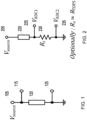
- Figure 1 is a diagram of a TOPS element 120, with a first electrical contact 115 and a second electrical contact 125, driven by a source 105 according to an exemplary embodiment of the disclosure.
- the source 105 is a voltage source.
- an electrical bias applied to a TOPS may determine the optical phase or transmission wavelength of the optical waveguides which are in thermal connection with the TOPS.
- a relationship between an optical phase or transmission wavelength and an applied power to a TOPS may be calibrated.
- R TOPS is a current value of the TOPS resistance.
- the value R TOPS taken at the time of the calculation above may differ from the resistance value R TOPS0 used at the TOPS BOL during calibration due to changes in temperature or normal aging of the TOPS.
- the electrical resistance R TOPS of the TOPS needs be monitored to periodically calculate the applicable source voltage, V source to accounts for TOPS resistance changes or other phenomena.
- FIG. 2 is a circuit diagram of a TOPS 220, driven by a source 205, and a series resistor 230 having a resistance R s according to an exemplary embodiment of the disclosure.
- an analog to digital converter may be used to monitor the voltage drop across the series resistor 230, i.e. the difference in voltages V ADC1 and V ADC2 , as a way to monitor the TOPS resistance R TOPS .
- the voltage drop may be measured at the two nodes or electrical contacts 225 and 235 that correspond to V ADC1 and V ADC2 , respectively.
- V source ⁇ P ⁇ R TOPS ⁇ R s + R TOPS
- R s is optionally selected or adjusted such that R s ⁇ R TOPS . The selection of R s ⁇ R TOPS allows the continuous monitoring of resistor 230 to be avoided and advantageously saves on hardware and power costs as discussed in more detail below.
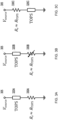
- Figure 3A is a diagram of a circuit configuration as disclosed herein that mitigates the effect of the change in electrical resistance R TOPS of the TOPS 320A on the variability of the calibration and obviates the need for real-time ADC monitoring according to an exemplary embodiment of the disclosure.
- the impedance of a given TOPS may be simulated as a resistor having a resistance R TOPS (or one or more resistors in some embodiments).
- the source 305 is a voltage source.
- a resistance R s 330A having a value substantially equal to the resistance of the TOPS R TOPS (taken at some moment in time, e.g.
- Rs may be used to designate the resistance of the resistor used in a given circuit such as the voltage divider configurations shown herein, and also used to identify or label the resistor itself.
- K is greater than about 0 and less than about 0.3. In some embodiments, K is greater than about 0 and less than about 0.2. In some embodiments, K is greater than about 0 and less than about 0.1. In some embodiments, K is greater than about 0 and less than about 0.05.
- Figure 3B is an alternative circuit configuration using a variable resistor 330B in series with the TOPS 320B according to an exemplary embodiment of the disclosure.
- a variable resistor may allow more precise matching of the series resistance R s and the TOPS resistance R TOPS at various stages of the device's fabrication or operation. For example, in some embodiments, given the advantages of having R s ⁇ R TOPS , the variable resistor having resistance R s may be set at R TOPS or about R TOPS or approximately R TOPS In various embodiments, R s may be selected (if fixed) or set (if variable) such that R s ⁇ R TOPS R TOPS is less than about 0.2. As shown in the embodiments, of Figures 3A and 3B , the resistor may be grounded.
- Figure 3C is an alternative circuit configuration wherein the TOPS and the resistor R s are reversed in position relative to the embodiments of Figure 3A or 3B .
- the TOPS 320C is the bottom element in the voltage divider and the resistor R s 330C is the top element in the voltage divider.
- one terminal or electrical contact of the TOPS 320C may be grounded as shown.
- the resistor R s is chosen in a manner similar to that of the embodiment of Figure 3A , i.e. R s ⁇ R TOPS or equivalently R s ⁇ R TOPS R TOPS ⁇ 0 .
- the various components disclosed herein may be electrically coupled or connected in various configurations that incorporate the voltage divider features and the advantages relative to TOPS bias stability and reliability over time.
- the TOPS may include one or more heating elements or devices such as, for example, a resistive heater.
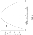
- Figure 4 is a plot 401 of a percent change in electrical power P (applied to the TOPS) versus a percent change in TOPS resistance R TOPS using a voltage divider configuration as disclosed herein, such as in Figures 3A, 3B, or 3C , wherein R s ⁇ R TOPS .
- a 10% change R TOPS produces a change of less than about 0.3% or less than about 0.2% in the power applied to the TOPS, under the same voltage source bias (at 305 as shown in Figures 3A, 3B, and 3C ) as calibration value.
- the TOPS circuit configuration enables stable electrical power bias on TOPS (change by less than about 0.3%), even if the TOPS resistance has changed dramatically.
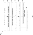
- Figure 5 is a flow chart of a method 500 for improving the stability of an electrical bias of a TOPS.
- the TOPS is then electrically coupled 511 to a voltage source.
- a resistor is then selected 515 having resistance R s chosen according to an optimization process wherein R s ⁇ R TOPS .
- the resistor is fixed or variable.
- the optimization process may including find a relative maxima or minima of the relationship of dP ⁇ dR TOPS as described above with regard to equation 6.
- the TOPS and the resistor are then electrically coupled in series to define or create a voltage divider configuration.
- the resultant circuit configuration stabilizes 523 the electrical power on TOPS and the optical phase tuning of the TOPS during temperature changes and device aging.
- such a voltage divider configuration furthermore avoids 527 continuous or periodic monitoring of the voltage drop across the TOPS and so also avoids additional area- and cost-consuming ADC channels dedicated to the TOPS.
- some aspects may be embodied as one or more methods.
- the acts performed as part of the method may be ordered in any suitable way. Accordingly, embodiments may be constructed in which acts are performed in an order different than illustrated, which may include performing some acts simultaneously, even though shown as sequential acts in illustrative embodiments.
- the phrase "at least one,” in reference to a list of one or more elements, should be understood to mean at least one element selected from any one or more of the elements in the list of elements, but not necessarily including at least one of each and every element specifically listed within the list of elements and not excluding any combinations of elements in the list of elements.
- This definition also allows that elements may optionally be present other than the elements specifically identified within the list of elements to which the phrase "at least one" refers, whether related or unrelated to those elements specifically identified.
- the terms “approximately” and “about” may be used to mean within ⁇ 20% of a target value in some embodiments, within ⁇ 10% of a target value in some embodiments, within ⁇ 5% of a target value in some embodiments, and yet within ⁇ 2% of a target value in some embodiments.
- the terms “approximately” and “about” may include the target value.
- each intervening value between the upper and lower limits of that range or list of values is individually contemplated and is encompassed within the disclosure as if each value were specifically enumerated herein.
- smaller ranges between and including the upper and lower limits of a given range are contemplated and encompassed within the disclosure.
- the listing of exemplary values or ranges is not a disclaimer of other values or ranges between and including the upper and lower limits of a given range.
- Embodiments disclosed herein may be embodied as a system, method or computer program product. Accordingly, embodiments may take the form of an entirely hardware embodiment, an entirely software embodiment (including firmware, resident software, microcode, etc.) or an embodiment combining software and hardware aspects that may all generally be referred to herein as a "circuit,” “module,” or “system.” Furthermore, embodiments may take the form of a computer program product embodied in one or more computer readable medium(s) having computer readable program code embodied thereon.
Landscapes
- Physics & Mathematics (AREA)
- Nonlinear Science (AREA)
- General Physics & Mathematics (AREA)
- Optics & Photonics (AREA)
- Optical Modulation, Optical Deflection, Nonlinear Optics, Optical Demodulation, Optical Logic Elements (AREA)
Abstract
In part, the disclosure relates to opto-electrical system. The system may include a waveguide defining an optical input and an optical output; a thermo-optic phase shifter (TOPS) that includes a first electrical contact and a second electrical contact, and a resistive heater in electrical communication with the first electrical contact and the second electrical contact, the TOPS configured to change a first phase of light entering the optical input to a second phase for light exiting the optical output, the TOPS having a resistance R TOPS , the TOPS in thermal communication with the waveguide; a voltage source in electrical communication with the first electrical contact; and a resistor that includes a first end and a second end, the resistor having a resistance RS, wherein the first end is grounded, wherein the second end is in electrical communication with the second electrical contact.
Description
- This disclosure relates generally to the field of photonic integrated circuits.
- Contemporary photonic systems make extensive use of photonic integrated circuits that are advantageously mass-produced in various configurations for various purposes.
- In part, in one aspect, the disclosure relates to a thermos optic phase shifter (TOPS) system and methods that stabilize the electrical bias applied to the TOPS. In one aspect, the disclosure relates to a TOPS in a voltage divider circuit configuration with a series resistance chosen to match the electrical resistance of the TOPS.
- In part, the disclosure relates to opto-electrical system. The system may include a waveguide defining an optical input and an optical output; a thermo-optic phase shifter (TOPS) that includes a first electrical contact and a second electrical contact, and a resistive heater in electrical communication with the first electrical contact and the second electrical contact, the TOPS configured to change a first phase of light entering the optical input to a second phase for light exiting the optical output, the TOPS having a resistance RTOPS, the TOPS in thermal communication with the waveguide; a voltage source in electrical communication with the first electrical contact; and a resistor that includes a first end and a second end, the resistor having a resistance RS, wherein the first end is grounded, wherein the second end is in electrical communication with the second electrical contact.
- In some embodiments, Rs is substantially equal to R TOPS. In some embodiments,

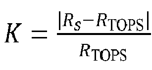
- In some embodiments, the resistive heater is in electrical communication with the voltage source and the resistor, wherein the resistive heater is configured to generate heat when electrical power is applied thereto, wherein a heating temperature of the resistive heater increases with application of increasing electrical power. In some embodiments, the system may include a photonic integrated circuit (PIC), wherein the TOPS is usually part of the PIC, and is in thermal communication with the PIC, wherein the PIC includes a device or is in communication with the device, wherein the device is selected from the group consisting of a laser, a transceiver, a variable optical attenuator, a tunable optical filter; a ring resonator; a phase tuner, a Mach-Zehnder interferometers (MZI), and a modulator.
- In another aspect, in part, the disclosure relates to a method of operating an electro-optical device with improved reliability thereof. The method may include providing a thermo-optic phase shifter (TOPS), the TOPS includes a first electrical contact and a second electrical contact; simulating an impedance between the first electrical contact and the second electrical contact of the TOPS as a resistance R TOPS; electrically coupling the first electrical contact to a voltage source; and selecting a resistor that includes a first end and a second end and having a resistance Rs such that when the first end is grounded and the second end is electrically coupled to the second electrical contact a power bias of the TOPS remains substantially stable during temperature changes of the TOPS.
- In some embodiments, substantially stable means or corresponds to electrical power applied to the TOPS from the voltage source being insensitive to TOPS resistance changes. In some embodiments, Rs is substantially equal to R TOPS. In many embodiments,
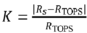

- In some embodiments, the electrical power of the TOPS may be determined using the following relationship


- In yet another aspect, in part, the disclosure relates to an opto-electrical system. The system may include a waveguide defining an optical input and an optical output; a thermo-optic phase shifter (TOPS) that includes a first electrical contact and a second electrical contact, the TOPS configured to change a first phase of light entering the optical input to a second phase of light, wherein light exiting the optical output is of the second phase, the TOPS having a resistance R TOPS,the TOPS in thermal communication with the waveguide, a resistor that includes a first end and a second end, the resistor having a resistance RS, wherein the first end is in electrical communication with the first electrical contact, wherein the second electrical contact is grounded; and a voltage source in electrical communication with the second end.
- Although, the disclosure relates to different aspects and embodiments, it is understood that the different aspects and embodiments disclosed herein can be integrated, combined, or used together as a combination system, or in part, as separate components, devices, and systems, as appropriate. Thus, each embodiment disclosed herein can be incorporated in each of the aspects to varying degrees as appropriate for a given implementation. Further, the various apparatus, optical elements, passivation coatings / layers, optical paths, waveguides, splitters, couplers, combiners, electro-optical devices, thermo-optic phase shifters, voltage sources, resistors, heaters, photonic integrated circuits (PICs), inputs, outputs, ports, channels, components and parts of the foregoing disclosed herein can be used with any laser, laser-based communication system, waveguide, fiber, transmitter, transceiver, receiver, and other devices and systems without limitation.
- These and other features of the applicant's teachings are set forth herein.
- Unless specified otherwise, the accompanying drawings illustrate aspects of the innovations described herein. Referring to the drawings, wherein like numerals refer to like parts throughout the several views and this specification, several embodiments of presently disclosed principles are illustrated by way of example, and not by way of limitation. The drawings are not intended to be to scale. A more complete understanding of the disclosure may be realized by reference to the accompanying drawings in which:
-
Figure 1 is a circuit diagram of a thermo-optic phase shifter (TOPS) with marked nodes at the electrical contacts of the TOPS according to an exemplary embodiment of the disclosure. -
Figure 2 is a circuit diagram of a TOPS and a series resistance designed to measure a change in a TOPS resistance via an analog-to-digital converter (ADC) according to an exemplary embodiment of the disclosure. -
Figure 3A is a circuit diagram of a voltage divider wherein the bottom resistor is selected to have resistance that matches the electrical resistance of the TOPS within various permitted variations according to an exemplary embodiment of the disclosure. -
Figure 3B is a circuit diagram of a TOPS in a voltage divider wherein the bottom resistor is a variable resistor according to an exemplary embodiment of the disclosure. -
Figure 3C is a circuit diagram of a TOPS in a voltage divider wherein the TOPS and the resistor are in an alternative configuration according to an exemplary embodiment of the disclosure. -
Figure 4 is a plot of a percent change in power applied to a TOPS versus a percent change in an electrical resistance of a TOPS according to an exemplary embodiment of the disclosure. -
Figure 5 is a flow chart of an exemplary method suitable for improving stability of a TOPS according to an exemplary embodiment of the disclosure. - In many embodiments, a thermo-optic phase shifter (TOPS) may be used with or integrated with a waveguide that has an optical input and an optical output. In most embodiments, the TOPS is in thermal communication with a waveguide and/or other electro-optical devices. In most embodiments, the TOPS has two electrical connections such a first electrical contact and a second electrical contact. An applied electrical bias, e.g. from an external voltage source, across the electrical contacts may change a phase of light entering at the optical input to a new optical phase of light exiting from the optical output. As such, in many embodiments, a TOPS may be used in conjunction with or to tune other optical devices such as Mach-Zehnder interferometers (MZI), ring resonators, external-cavity lasers, tunable optical filters, variable optical attenuators, optical modulators, phase tuners, optical transceivers etc.
- Refer now to the exemplary embodiment of
Figure 1. Figure 1 is a diagram of aTOPS element 120, with a firstelectrical contact 115 and a secondelectrical contact 125, driven by asource 105 according to an exemplary embodiment of the disclosure. In various embodiments, thesource 105 is a voltage source. In many embodiments, an electrical bias applied to a TOPS may determine the optical phase or transmission wavelength of the optical waveguides which are in thermal connection with the TOPS. In many embodiments, a relationship between an optical phase or transmission wavelength and an applied power to a TOPS may be calibrated. In some embodiments, a calibration may be performed by measuring an optical phase ϕ at the optical output and by calculating an electrical power P(ϕ) corresponding to an applied voltage V source:
- Conversely, in many embodiments, by using a calibrated relationship P(ϕ), a source voltage V source suitable to achieve a particular optical phase ϕ may be calculated as

- Refer now to the example embodiment of
Figure 2. Figure 2 is a circuit diagram of aTOPS 220, driven by asource 205, and aseries resistor 230 having a resistance Rs according to an exemplary embodiment of the disclosure. In some embodiments, an analog to digital converter (ADC) may be used to monitor the voltage drop across theseries resistor 230, i.e. the difference in voltages V ADC1 and V ADC2, as a way to monitor the TOPS resistance R TOPS. The voltage drop may be measured at the two nodes orelectrical contacts 


resistor 230 to be avoided and advantageously saves on hardware and power costs as discussed in more detail below. - Refer now to the exemplary embodiment of
Figure 3A. Figure 3A is a diagram of a circuit configuration as disclosed herein that mitigates the effect of the change in electrical resistance R TOPS of theTOPS 320A on the variability of the calibration and obviates the need for real-time ADC monitoring according to an exemplary embodiment of the disclosure. In some embodiments, the impedance of a given TOPS may be simulated as a resistor having a resistance R TOPS (or one or more resistors in some embodiments). Thesource 305 is a voltage source. In many embodiments, aresistance R s 330A having a value substantially equal to the resistance of the TOPS R TOPS (taken at some moment in time, e.g. at BOL) may be added in series with the TOPS or otherwise electrically coupled thereto to form a voltage divider configuration. In most embodiments, when Rs ≈ R TOPS, or equivalently when a ratio


- Refer also to the embodiment of
Figure 3B. Figure 3B is an alternative circuit configuration using avariable resistor 330B in series with theTOPS 320B according to an exemplary embodiment of the disclosure. A variable resistor may allow more precise matching of the series resistance Rs and the TOPS resistance R TOPS at various stages of the device's fabrication or operation. For example, in some embodiments, given the advantages of having Rs ≈ R TOPS, the variable resistor having resistance Rs may be set at R TOPS or about R TOPS or approximately R TOPS In various embodiments, Rs may be selected (if fixed) or set (if variable) such that
Figures 3A and 3B , the resistor may be grounded. - Refer also to the embodiment of
Figure 3C. Figure 3C is an alternative circuit configuration wherein the TOPS and the resistor Rs are reversed in position relative to the embodiments ofFigure 3A or 3B . As shown, theTOPS 320C is the bottom element in the voltage divider and theresistor R s 330C is the top element in the voltage divider. In some embodiments, one terminal or electrical contact of theTOPS 320C may be grounded as shown. In the embodiment ofFigure 3C , the resistor Rs is chosen in a manner similar to that of the embodiment ofFigure 3A , i.e. Rs ≈ R TOPS or equivalently
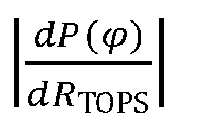
Figure 3C remains substantially stable. In general, in various embodiments, the various components disclosed herein may be electrically coupled or connected in various configurations that incorporate the voltage divider features and the advantages relative to TOPS bias stability and reliability over time. In various embodiments, the TOPS may include one or more heating elements or devices such as, for example, a resistive heater. - Refer now to
Figure 4. Figure 4 is aplot 401 of a percent change in electrical power P (applied to the TOPS) versus a percent change in TOPS resistance R TOPS using a voltage divider configuration as disclosed herein, such as inFigures 3A, 3B, or 3C , wherein Rs ≈ R TOPS. According toFigure 4 , a 10% change R TOPS produces a change of less than about 0.3% or less than about 0.2% in the power applied to the TOPS, under the same voltage source bias (at 305 as shown inFigures 3A, 3B, and 3C ) as calibration value. In short, the TOPS circuit configuration enables stable electrical power bias on TOPS (change by less than about 0.3%), even if the TOPS resistance has changed dramatically. - Refer now to
Figure 5. Figure 5 is a flow chart of amethod 500 for improving the stability of an electrical bias of a TOPS. In many embodiments, a providedTOPS 503 is first measured 507 to obtain a resistance R TOPS, where R TOPS = R TOPS0 if the measurement is taken at the TOPS BOL. In most embodiments, the TOPS is then electrically coupled 511 to a voltage source. In most embodiments, a resistor is then selected 515 having resistance Rs chosen according to an optimization process wherein Rs ≈ R TOPS. In some embodiments, the resistor is fixed or variable. In some embodiments, the optimization process may including find a relative maxima or minima of the relationship of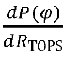
- Having thus described several aspects and embodiments of the technology of this application, it is to be appreciated that various alterations, modifications, and improvements will readily occur to those of ordinary skill in the art. Such alterations, modifications, and improvements are intended to be within the spirit and scope of the technology described in the application. It is, therefore, to be understood that the foregoing embodiments are presented by way of example only and that, within the scope of the appended claims and equivalents thereto, inventive embodiments may be practiced otherwise than as specifically described. In addition, any combination of two or more features, systems, articles, materials, and/or methods described herein, if such features, systems, articles, materials, and/or methods are not mutually inconsistent, is included within the scope of the present disclosure.
- Also, as described, some aspects may be embodied as one or more methods. The acts performed as part of the method may be ordered in any suitable way. Accordingly, embodiments may be constructed in which acts are performed in an order different than illustrated, which may include performing some acts simultaneously, even though shown as sequential acts in illustrative embodiments.
- The phrase "and/or," as used herein in the specification and in the claims, should be understood to mean "either or both" of the elements so conjoined, i.e., elements that are conjunctively present in some cases and disjunctively present in other cases.
- As used herein in the specification and in the claims, the phrase "at least one," in reference to a list of one or more elements, should be understood to mean at least one element selected from any one or more of the elements in the list of elements, but not necessarily including at least one of each and every element specifically listed within the list of elements and not excluding any combinations of elements in the list of elements. This definition also allows that elements may optionally be present other than the elements specifically identified within the list of elements to which the phrase "at least one" refers, whether related or unrelated to those elements specifically identified.
- The terms "approximately" and "about" may be used to mean within ±20% of a target value in some embodiments, within ±10% of a target value in some embodiments, within ±5% of a target value in some embodiments, and yet within ±2% of a target value in some embodiments. The terms "approximately" and "about" may include the target value.
- In the claims, as well as in the specification above, all transitional phrases such as "comprising," "including," "carrying," "having," "containing," "involving," "holding," "composed of," and the like are to be understood to be open-ended, i.e., to mean including but not limited to. The transitional phrases "consisting of' and "consisting essentially of' shall be closed or semi-closed transitional phrases, respectively.
- Where a range or list of values is provided, each intervening value between the upper and lower limits of that range or list of values is individually contemplated and is encompassed within the disclosure as if each value were specifically enumerated herein. In addition, smaller ranges between and including the upper and lower limits of a given range are contemplated and encompassed within the disclosure. The listing of exemplary values or ranges is not a disclaimer of other values or ranges between and including the upper and lower limits of a given range.
- The use of headings and sections in the application is not meant to limit the disclosure; each section can apply to any aspect, embodiment, or feature of the disclosure. Only those claims which use the words "means for" are intended to be interpreted under 35 USC 112. Absent a recital of "means for" in the claims, such claims should not be construed under 35 USC 112. Limitations from the specification are not intended to be read into any claims, unless such limitations are expressly included in the claims.
- Embodiments disclosed herein may be embodied as a system, method or computer program product. Accordingly, embodiments may take the form of an entirely hardware embodiment, an entirely software embodiment (including firmware, resident software, microcode, etc.) or an embodiment combining software and hardware aspects that may all generally be referred to herein as a "circuit," "module," or "system." Furthermore, embodiments may take the form of a computer program product embodied in one or more computer readable medium(s) having computer readable program code embodied thereon.
Claims (14)
- An opto-electrical system comprising:a waveguide defining an optical input and an optical output;a thermo-optic phase shifter, TOPS, comprisinga first electrical contact and a second electrical contact, anda resistive heater in electrical communication with the first electrical contact and the second electrical contact,the TOPS configured to change a first phase of light entering the optical input to a second phase for light exiting the optical output,the TOPS having a resistance R TOPS,the TOPS in thermal communication with the waveguide;a voltage source in electrical communication with the first electrical contact; anda resistor comprising a first end and a second end, the resistor having a resistance RS, wherein the first end is grounded, wherein the second end is in electrical communication with the second electrical contact.
- The system of claim 1, wherein Rs is substantially equal to R TOPS.
- The system of claim 1 or 2, wherein

- The system of any preceding claim, wherein the resistor is a variable resistor and Rs is a variable resistance, optionally wherein one or more of:A) Rs is selected such that Rs is approximately the same as RTOPS;B) Rs is selected such that K is less than or equal to about 0.2, wherein

- The system of any preceding claim, wherein Rs is selected to stabilize power bias applied to TOPS from voltage source during aging of TOPS or temperature changes of the TOPS.
- The system of any preceding claim, wherein Rs ranges from about 1 ohm to about 1,000 ohms.
- The system of any preceding claim, wherein the resistive heater is in electrical communication with the voltage source and the resistor, wherein the resistive heater is configured to generate heat when electrical power is applied thereto, wherein a heating temperature of the resistive heater increases with application of increasing electrical power.
- The system of any preceding claim further comprising a photonic integrated circuit, PIC, wherein the TOPS is usually part of the PIC, and is in thermal communication with the PIC, wherein the PIC comprises a device or is in communication with the device, wherein the device is selected from the group consisting of a laser, a transceiver, a variable optical attenuator, a tunable optical filter; a ring resonator; a phase tuner, a Mach-Zehnder interferometers, MZI, and a modulator.
- A method of operating an electro-optical device with improved reliability thereof, the method comprising:providing a thermo-optic phase shifter, TOPS, the TOPS comprising a first electrical contact and a second electrical contact;simulating an impedance between the first electrical contact and the second electrical contact of the TOPS as a resistance R TOPS;electrically coupling the first electrical contact to a voltage source; andselecting a resistor comprising a first end and a second end and having a resistance Rs such that when the first end is grounded and the second end is electrically coupled to the second electrical contact a power bias of the TOPS remains substantially stable during temperature changes of the TOPS.
- The method of claim 9, wherein one or more of:A) substantially stable means or corresponds to electrical power applied to the TOPS from the voltage source being insensitive to TOPS resistance changes;B)wherein Rs is substantially equal to R TOPS;C)
 D) the resistor is a variable resistor and Rs is a variable resistance, further comprising the step of adjusting Rs until
 E) the TOPS remaining substantially stable avoids measuring voltage source corresponding to identify changes in R TOPS over time due to aging or temperature changes of the TOPS.
 - The method of claim 9 or 10, wherein the electrical power of the TOPS may be determined using the following relationship


the method optionally further comprising selecting Rs to be approximately equal to R TOPS is determined by finding a zero value of
- The method of any of claims 9 to 11, further comprising integrating the TOPS into a photonic integrated circuit.
- The method of claims 9 to 12, wherein when the TOPS resistance changes by 10%, under the same voltage source bias, the electrical power applied to the TOPS changes by an amount less than or equal to about 0.3% or less than or equal to about 0.2%.
- An opto-electrical system comprising:a waveguide defining an optical input and an optical output;a thermo-optic phase shifter, TOPS, comprising
a first electrical contact and a second electrical contact,the TOPS configured to change a first phase of light entering the optical input to a second phase of light, wherein light exiting the optical output is of the second phase,the TOPS having a resistance R TOPS,the TOPS in thermal communication with the waveguide,a resistor comprising a first end and a second end, the resistor having a resistance RS, wherein the first end is in electrical communication with the first electrical contact, wherein the second electrical contact is grounded; anda voltage source in electrical communication with the second end.
Applications Claiming Priority (1)
| Application Number | Priority Date | Filing Date | Title |
|---|---|---|---|
| US18/114,761 US12481181B2 (en) | 2023-02-27 | 2023-02-27 | Thermo-optic phase shifter systems and methods |
Publications (1)
| Publication Number | Publication Date |
|---|---|
| EP4421555A1 true EP4421555A1 (en) | 2024-08-28 |
Family
ID=90059443
Family Applications (1)
| Application Number | Title | Priority Date | Filing Date |
|---|---|---|---|
| EP24159610.5A Pending EP4421555A1 (en) | 2023-02-27 | 2024-02-26 | Thermo-optic phase shifter systems and methods field |
Country Status (2)
| Country | Link |
|---|---|
| US (2) | US12481181B2 (en) |
| EP (1) | EP4421555A1 (en) |
Families Citing this family (2)
| Publication number | Priority date | Publication date | Assignee | Title |
|---|---|---|---|---|
| US12481181B2 (en) * | 2023-02-27 | 2025-11-25 | Cisco Technology, Inc. | Thermo-optic phase shifter systems and methods |
| US20240426676A1 (en) * | 2023-06-26 | 2024-12-26 | Cisco Technology, Inc. | Local silicon-photonics temperature sensor |
Citations (3)
| Publication number | Priority date | Publication date | Assignee | Title |
|---|---|---|---|---|
| CA2333635A1 (en) * | 1999-04-01 | 2000-10-12 | Jds Uniphase Corporation | Method and apparatus for stable control of electrooptic devices |
| US20050100260A1 (en) * | 2003-11-07 | 2005-05-12 | Nec Corporation | Optical waveguide device, variable optical attenuator, and optical switch |
| US20220365377A1 (en) * | 2019-06-24 | 2022-11-17 | Nippon Telegraph And Telephone Corporation | Optical Circuit |
Family Cites Families (6)
| Publication number | Priority date | Publication date | Assignee | Title |
|---|---|---|---|---|
| US20170336657A1 (en) * | 2014-11-18 | 2017-11-23 | Nec Corporation | A heater for optical waveguide and a method for configuring a heater for optical waveguide |
| US10353267B2 (en) * | 2016-12-30 | 2019-07-16 | Huawei Technologies Co., Ltd. | Carrier-effect based optical switch |
| US10394059B1 (en) * | 2018-12-14 | 2019-08-27 | Cisco Technology, Inc. | Thermo-optic phase shifter with thermal bridge |
| US20210157211A1 (en) * | 2019-11-21 | 2021-05-27 | Lightmatter, Inc. | Interferometric modulation |
| US12481181B2 (en) * | 2023-02-27 | 2025-11-25 | Cisco Technology, Inc. | Thermo-optic phase shifter systems and methods |
| US20240345300A1 (en) * | 2023-04-11 | 2024-10-17 | Ii-Vi Delaware, Inc. | Optical Polarizers with High Transmission, Corrosion Resistance and Reduced Thickness |
-
2023
- 2023-02-27 US US18/114,761 patent/US12481181B2/en active Active
-
2024
- 2024-02-26 EP EP24159610.5A patent/EP4421555A1/en active Pending
-
2025
- 2025-09-12 US US19/327,901 patent/US20260010021A1/en active Pending
Patent Citations (3)
| Publication number | Priority date | Publication date | Assignee | Title |
|---|---|---|---|---|
| CA2333635A1 (en) * | 1999-04-01 | 2000-10-12 | Jds Uniphase Corporation | Method and apparatus for stable control of electrooptic devices |
| US20050100260A1 (en) * | 2003-11-07 | 2005-05-12 | Nec Corporation | Optical waveguide device, variable optical attenuator, and optical switch |
| US20220365377A1 (en) * | 2019-06-24 | 2022-11-17 | Nippon Telegraph And Telephone Corporation | Optical Circuit |
Also Published As
| Publication number | Publication date |
|---|---|
| US12481181B2 (en) | 2025-11-25 |
| US20240288717A1 (en) | 2024-08-29 |
| US20260010021A1 (en) | 2026-01-08 |
Similar Documents
| Publication | Publication Date | Title |
|---|---|---|
| US20260010021A1 (en) | Thermo-optic phase shifter systems and methods | |
| Offrein et al. | Adaptive gain equalizer in high-index-contrast SiON technology | |
| US20090161113A1 (en) | Integrated optoelectronic system for automatic calibration of an optical device | |
| US12308601B1 (en) | Wavelength locker | |
| CN101969340B (en) | Adaptive compensation method for inhibiting bias point drift of Mach-Zehnder modulator | |
| EP1380865B1 (en) | Adjustment method for optical circuit with cascaded Mach-Zehnder interferometers | |
| TWI489713B (en) | Split control of front and rear dbr grating portions | |
| WO2010139144A1 (en) | Optical module and control method thereof | |
| US20170331550A1 (en) | Photonic-chip-based optical spectrum analyzer | |
| US20030174951A1 (en) | Multichannel integrated tunable thermo-optic lens and dispersion compensator | |
| Stern et al. | Athermal silicon photonic wavemeter for broadband and high-accuracy wavelength measurements | |
| Liu et al. | Continuously tunable silicon optical true-time delay lines with a large delay tuning range and a low delay fluctuation | |
| Shi et al. | Non-invasive delay state calibration of silicon optical switching delay line | |
| KR101828061B1 (en) | Optical interferometer structure and optical sensors incorporating multimode interference waveguide devices using of the same and signal processing method for the same | |
| US20030169964A1 (en) | Power splitter/combiner with parameter tolerance and design process therefor | |
| Amatya et al. | Precision tunable silicon compatible microring filters | |
| US20200025569A1 (en) | Device comprising a ring optical resonator | |
| US6243506B1 (en) | Optical frequency and temperature sensor system | |
| Chen et al. | Silicon-based integrated broadband wavelength-meter with low temperature sensitivity | |
| EP4624981A1 (en) | Optical phased array chip, control method, and optical waveguide phased array system | |
| Moreira | Integrated optical delay line circuits on a ultra-low loss planar waveguide platform | |
| CN115857109B (en) | Resonator systems, tunable lasers, and control methods for resonator systems | |
| US20100027936A1 (en) | Tuneable electro-optic modulator | |
| Morton et al. | High SFDR ‘Super-ring’microresonator based true-time-delay (TTD) | |
| CN120928624B (en) | Waveguide assembly, control method of waveguide assembly, optical chip and optical quantum computer |
Legal Events
| Date | Code | Title | Description |
|---|---|---|---|
| PUAI | Public reference made under article 153(3) epc to a published international application that has entered the european phase |
Free format text: ORIGINAL CODE: 0009012 |
|
| STAA | Information on the status of an ep patent application or granted ep patent |
Free format text: STATUS: THE APPLICATION HAS BEEN PUBLISHED |
|
| AK | Designated contracting states |
Kind code of ref document: A1 Designated state(s): AL AT BE BG CH CY CZ DE DK EE ES FI FR GB GR HR HU IE IS IT LI LT LU LV MC ME MK MT NL NO PL PT RO RS SE SI SK SM TR |
|
| STAA | Information on the status of an ep patent application or granted ep patent |
Free format text: STATUS: REQUEST FOR EXAMINATION WAS MADE |
|
| 17P | Request for examination filed |
Effective date: 20250224 |