EP4421398A1 - Control device and air conditioning device - Google Patents
Control device and air conditioning device Download PDFInfo
- Publication number
- EP4421398A1 EP4421398A1 EP22883661.5A EP22883661A EP4421398A1 EP 4421398 A1 EP4421398 A1 EP 4421398A1 EP 22883661 A EP22883661 A EP 22883661A EP 4421398 A1 EP4421398 A1 EP 4421398A1
- Authority
- EP
- European Patent Office
- Prior art keywords
- control board
- control
- unit
- voltage
- circuit
- Prior art date
- Legal status (The legal status is an assumption and is not a legal conclusion. Google has not performed a legal analysis and makes no representation as to the accuracy of the status listed.)
- Granted
Links
Images



Classifications
-
- F—MECHANICAL ENGINEERING; LIGHTING; HEATING; WEAPONS; BLASTING
- F24—HEATING; RANGES; VENTILATING
- F24F—AIR-CONDITIONING; AIR-HUMIDIFICATION; VENTILATION; USE OF AIR CURRENTS FOR SCREENING
- F24F11/00—Control or safety arrangements
- F24F11/88—Electrical aspects, e.g. circuits
-
- F—MECHANICAL ENGINEERING; LIGHTING; HEATING; WEAPONS; BLASTING
- F24—HEATING; RANGES; VENTILATING
- F24F—AIR-CONDITIONING; AIR-HUMIDIFICATION; VENTILATION; USE OF AIR CURRENTS FOR SCREENING
- F24F11/00—Control or safety arrangements
- F24F11/50—Control or safety arrangements characterised by user interfaces or communication
- F24F11/54—Control or safety arrangements characterised by user interfaces or communication using one central controller connected to several sub-controllers
-
- F—MECHANICAL ENGINEERING; LIGHTING; HEATING; WEAPONS; BLASTING
- F24—HEATING; RANGES; VENTILATING
- F24F—AIR-CONDITIONING; AIR-HUMIDIFICATION; VENTILATION; USE OF AIR CURRENTS FOR SCREENING
- F24F11/00—Control or safety arrangements
- F24F11/89—Arrangement or mounting of control or safety devices
-
- H—ELECTRICITY
- H02—GENERATION; CONVERSION OR DISTRIBUTION OF ELECTRIC POWER
- H02M—APPARATUS FOR CONVERSION BETWEEN AC AND AC, BETWEEN AC AND DC, OR BETWEEN DC AND DC, AND FOR USE WITH MAINS OR SIMILAR POWER SUPPLY SYSTEMS; CONVERSION OF DC OR AC INPUT POWER INTO SURGE OUTPUT POWER; CONTROL OR REGULATION THEREOF
- H02M1/00—Details of apparatus for conversion
- H02M1/0003—Details of control, feedback or regulation circuits
- H02M1/0006—Arrangements for supplying an adequate voltage to the control circuit of converters
-
- H—ELECTRICITY
- H02—GENERATION; CONVERSION OR DISTRIBUTION OF ELECTRIC POWER
- H02M—APPARATUS FOR CONVERSION BETWEEN AC AND AC, BETWEEN AC AND DC, OR BETWEEN DC AND DC, AND FOR USE WITH MAINS OR SIMILAR POWER SUPPLY SYSTEMS; CONVERSION OF DC OR AC INPUT POWER INTO SURGE OUTPUT POWER; CONTROL OR REGULATION THEREOF
- H02M1/00—Details of apparatus for conversion
- H02M1/0003—Details of control, feedback or regulation circuits
- H02M1/0032—Control circuits allowing low power mode operation, e.g. in standby mode
-
- F—MECHANICAL ENGINEERING; LIGHTING; HEATING; WEAPONS; BLASTING
- F24—HEATING; RANGES; VENTILATING
- F24F—AIR-CONDITIONING; AIR-HUMIDIFICATION; VENTILATION; USE OF AIR CURRENTS FOR SCREENING
- F24F11/00—Control or safety arrangements
- F24F11/30—Control or safety arrangements for purposes related to the operation of the system, e.g. for safety or monitoring
-
- F—MECHANICAL ENGINEERING; LIGHTING; HEATING; WEAPONS; BLASTING
- F24—HEATING; RANGES; VENTILATING
- F24F—AIR-CONDITIONING; AIR-HUMIDIFICATION; VENTILATION; USE OF AIR CURRENTS FOR SCREENING
- F24F11/00—Control or safety arrangements
- F24F11/62—Control or safety arrangements characterised by the type of control or by internal processing, e.g. using fuzzy logic, adaptive control or estimation of values
- F24F11/63—Electronic processing
-
- F—MECHANICAL ENGINEERING; LIGHTING; HEATING; WEAPONS; BLASTING
- F24—HEATING; RANGES; VENTILATING
- F24F—AIR-CONDITIONING; AIR-HUMIDIFICATION; VENTILATION; USE OF AIR CURRENTS FOR SCREENING
- F24F3/00—Air-conditioning systems in which conditioned primary air is supplied from one or more central stations to distributing units in the rooms or spaces where it may receive secondary treatment; Apparatus specially designed for such systems
- F24F3/06—Air-conditioning systems in which conditioned primary air is supplied from one or more central stations to distributing units in the rooms or spaces where it may receive secondary treatment; Apparatus specially designed for such systems characterised by the arrangements for the supply of heat-exchange fluid for the subsequent treatment of primary air in the room units
- F24F3/065—Air-conditioning systems in which conditioned primary air is supplied from one or more central stations to distributing units in the rooms or spaces where it may receive secondary treatment; Apparatus specially designed for such systems characterised by the arrangements for the supply of heat-exchange fluid for the subsequent treatment of primary air in the room units with a plurality of evaporators or condensers
Definitions
- the present disclosure relates to a control device, and an air conditioner including the control device.
- An air conditioner includes an outdoor unit and an indoor unit each of which typically has a control board equipped with a microcomputer (see PATENT LITERATURE 1 or the like).
- the microcomputers on the two control boards are connected via a transmission line, so as to communicate with each other.
- a single outdoor unit may be provided with a plurality of control boards.
- PATENT LITERATURE 1 Japanese Laid-Open Patent Publication No. 2001-41530
- Provision of the plurality of control boards needs a power source circuit for delivery of DC voltage necessary on each of the boards from an external commercial AC power source. This increases the total number of components necessary for the power source circuit.
- the second control board needs neither a noise filter nor an AC-DC converter, so as to achieve reduction in the number of components relevant to a power source circuit. Accordingly, the number of components can be reduced even in a case where a single apparatus is equipped with a plurality of control boards.
- the first control board and the second control board are preferably accommodated in a common case.
- the second control board includes a communication circuit configured to execute communication between the first control unit and the second control unit by means of a current signal
- the communication circuit includes an input unit configured to provide an input signal from the first control board to the second control unit, an output unit connected in series to the input unit and configured to output an output signal from the second control unit to the first control board, and a bypass circuit provided in parallel with the output unit and including a first switch, and the second control unit closes the first switch when coming into a sleep mode and opens the first switch when cancelling the sleep mode.
- the bypass circuit is formed to keep the communication circuit by means of a current signal even in a case where there is another control board provided for an additional function and configured similarly to the second control board.
- the first switch is a semiconductor switch or the like, and resistance is connected in series on a positive potential side from a control terminal.
- This case enables inhibition of control current flowing to the semiconductor switch.
- Electric current can reliably flow to the bypass circuit in this case.
- the second control unit exemplarily controls a function of ventilation, humidification, or washing.
- Such a function can be achieved by the second control unit independently from the first control unit.
- the second control board includes a switching power source to be supplied with the DC voltage, and the switching power source has an output side provided with a second switch.
- the second control board opens the second switch so as to inhibit power consumption.
- An air conditioner includes the control device according to (1) to (7) described above.
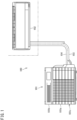
- FIG. 1 is a diagram depicting exemplary outer appearance of an air conditioner 100.
- the air conditioner 100 includes an outdoor unit 101 and an indoor unit 102.
- the outdoor unit 101 includes a case 101c constituted by a body unit 101a having a built-in refrigerant circuit, and a ventilating-humidifying unit 101b provided thereon.
- the case 101c mentioned herein corresponds to an outer package portion having maximum size of the outdoor unit 101, and does not matter whether or not to have an internal partition.
- the outdoor unit 101 and the indoor unit 102 are connected via a refrigerant pipe 103 and an air pipe 104.
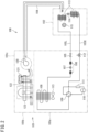
- FIG. 2 is a functional schematic view of the air conditioner 100.
- the body unit 101a of the outdoor unit 101 includes, in the mentioned order, a liquid shutoff valve 105, a filter 106, an expansion valve 107, a heat exchanger 108, a four-way switching valve 109, a compressor 110, an accumulator 111, and a gas shutoff valve 112, which constitute a known refrigerant circuit connected as depicted.
- the heat exchanger 108 is provided with a fan 113 for ventilation.
- the indoor unit 102 includes a heat exchanger 113, an expansion valve 114, and a fan 115, which are connected as depicted.
- the outdoor unit 101 and the indoor unit 102 are connected to each other via a liquid refrigerant tube 103L and a gas refrigerant tube 103G.
- the ventilating-humidifying unit 101b includes an intake-exhaust fan 120, a heater 121, a humidifying rotor 122, and an adsorption fan 123.
- the ventilating-humidifying unit 101b is configured to discharge outdoors indoor air introduced into the indoor unit 102, and add moisture to fresh outdoor air and send indoors the air thus humidified. In winter, the ventilating-humidifying unit 101b is configured to introduce indoors air heated with use of the heater 121.
- the ventilating-humidifying unit 101b is connected with the indoor unit 102 via the air pipe 104.
- the body unit 101a of the outdoor unit 101 operates in accordance with an own basic microcomputer to be described later.
- the ventilating-humidifying unit 101b operates in accordance with an own functional microcomputer to be described later.
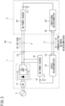
- FIG. 3 is a circuit connection diagram depicting an exemplary center part of a control device 50 in the air conditioner 100.
- This figure depicts control boards each constituted by a printed circuit board.
- the control boards include a basic control board 1 (first control board) having a control function of achieving basic operation as the air conditioner 100, and a functional control board 2 (second control board) having a control function of achieving an additional function.
- the functional control board 2 is provided separately and is different from the basic control board 1. Though the figure depicts the single functional control board 2, there may occasionally be provided a plurality of functional control boards.
- the basic control board 1 is connected with an external AC power source 3.
- the basic control board 1 is provided thereon with a noise filter 11, an AC-DC converter 14 including a rectifier circuit 12 and a smoothing capacitor 13, a terminal block 15 for external power supply, a switching power source 16, a capacitor 17, a basic microcomputer (first control unit) 18, and an interface circuit 19, which are connected as depicted.
- the noise filter 11 inhibits noise leakage from the basic control board 1 to the AC power source 3.
- the AC-DC converter 14 rectifies by voltage doubling and smooths AC voltage (e.g. 100 V) to obtain DC voltage (about 280 V). Rectification by voltage doubling is merely exemplary, and the AC-DC converter has only to be a circuit configured to rectify and smooth AC voltage. This DC voltage is stepped down to predetermined voltage by the switching power source 16, for supply of stable control voltage to the basic microcomputer 18.
- the basic microcomputer 18 achieves basic operation as the air conditioner 100 in accordance with software. The software is stored in a memory (not depicted) equipped in the basic microcomputer 18.
- the functional control board 2 is connected with the basic control board 1 via DC output wiring 4.
- the DC output wiring 4 supplies the functional control board 2 with DC voltage.
- the functional control board 2 is provided thereon with a switching power source 26, a capacitor 27, a functional microcomputer (second control unit) 28, and an interface circuit 29, which are connected as depicted.
- the DC voltage supplied from the DC output wiring 4 is stepped down to predetermined voltage by the switching power source 26, for supply of stable control voltage to the functional microcomputer 28.
- the functional microcomputer 28 achieves additional functional operation as the air conditioner 100 in accordance with software.
- the software is stored in a memory (not depicted) equipped in the functional microcomputer 28.
- the basic microcomputer 18 and the functional microcomputer 28 are connected to each other via the interface circuit 19, a transmission line 5, and the interface circuit 29, to execute communication between microcomputers.
- the functional control board 2 is configured to control a function of ventilation, humidification, washing, or the like, independently from the basic control board 1.
- the control device 50 depicted in FIG. 3 separately includes the basic control board 1 for achievement of basic functions and the functional control board 2 for achievement of additional functions, so as to prepare various additional functions by the functional control board 2.
- the functional control board 2 needs neither a noise filter nor an AC-DC converter, so as to achieve reduction in the number of components relevant to a power source circuit.
- the basic control board 1 and the functional control board 2 are both accommodated in the common case 101c ( FIG. 1 ).
- the both control boards 1 and 2 accommodated in the common case are disposed relatively close to each other, so as to inhibit noise generated on a communication circuit (the interface circuit 19, the transmission line 5, and the interface circuit 29) configured to execute communication between the basic microcomputer 18 and the functional microcomputer 28.
- FIG. 4 is a circuit diagram depicting a communication circuit 6 for communication between microcomputers.
- FIG. 3 exemplifies communication between the basic microcomputer 18 and the functional microcomputer 28 as one-to-one relation, whereas FIG. 4 depicts a case where there are provided two (exemplifying a plurality of) functional control boards.
- an additional functional control board 2x includes a functional microcomputer 28x and an interface circuit 29x.
- the communication circuit 6 is provided as a closed circuit configured to cause a current signal to flow in a time dividing manner.
- the communication circuit 6 constituted by the interface circuits 19, 29, and 29x is configured to cause electric current to flow in a looped manner.
- the microcomputers each have operation states including a normal mode of operating at high speed and a sleep mode of operating at low speed for functional inhibition and power saving.
- FIG. 5 is a circuit diagram depicting the interface circuit 29 on the functional control board 2 according to the first example.
- the interface circuit 29 includes a photocoupler 291 functioning as an input unit for a signal transmitted from the basic microcomputer 18, a reception circuit 292, a photocoupler 293 functioning as an output unit for a signal to be transmitted to the basic microcomputer 18, a transmission circuit 294, and a bypass circuit (also called an ACS through circuit) 295.
- the bypass circuit 295 is configured to short-circuit and invalidate both ends of the output unit 293 in the sleep mode.
- an input signal ACS_INPUT is provided to the functional microcomputer 28 via the reception circuit 292.
- the functional microcomputer 28 outputs an output signal ACS_OUTPUT that turns ON or OFF the photocoupler 293 via the transmission circuit 294.
- the bypass circuit 295 is constituted by a drive circuit 295a, a photocoupler 295b, resistance 295c, and a transistor 295d, which are connected as depicted.
- Examples of the resistance 295c has high resistance of about 24 kS2.
- An ACS_THRU signal has an H level when the functional microcomputer 28 is in the normal mode (operating at high speed), and has an L level when the functional microcomputer 28 is in the sleep mode (operating at low speed).
- the drive circuit 295a turns ON the photocoupler 295b.
- the transistor 295d is in an OFF state because the transistor 295d has no voltage generated between a base and an emitter, and the communication circuit 6 ( FIG. 4 ) has electric current flowing through the photocoupler 293.
- the photocoupler 293 is ready to output a signal.
- the bypass circuit 295 has electric current flowing from the resistance 295c and passing the photocoupler 295b. The electric current is quite small because the resistance 295c has a high resistance value.
- the drive circuit 295a turns OFF the photocoupler 295b.
- the transistor 295d is in an ON state because the transistor 295d has voltage applied between the base and the emitter via the resistance 295c.
- the photocoupler 293 is bypassed by the transistor 295d connected in parallel, and the photocoupler 293 includes a phototransistor 293d being short-circuited.
- the functional microcomputer 28 has an output port (a port for ACS_OUTPUT) thus invalidated.
- the switching power source 26 supplies power to a device other than the functional microcomputer 28, and exemplarily supplies voltage of 5 V to a load 31a via a switch 30a. Similarly, the switching power source 26 supplies voltage of 14 V to a load 31b via a switch 30b, and supplies voltage of 15 V to a load 31c via a switch 30c.
- the functional microcomputer 28 is configured to control to turn ON or OFF the switches 30a, 30b, and 30c with use of an output port 281.
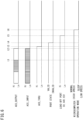
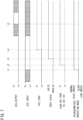
- FIG. 6 is an exemplary timing chart in a case where the functional microcomputer 28 comes into the sleep mode from the normal mode.
- the timing chart indicates, in the mentioned order from the top, ACS_OUTPUT, ACS_INPUT, ACS_THRU, a port state, a load off port (5 V, 14 V, 15 V), and a microcomputer operation mode.
- the port state indicates whether the output port (the port for ACS_OUTPUT) is valid or invalid. When the port state is invalid, an input port is also invalid except for microcomputer reset and ACS_INPUT.
- the load off port corresponds to the output port 281.
- ACS_THRU has the H level, and the port for ACS_OUTPUT is valid.
- the load off port also has the H level, and the switches 30a, 30b, and 30c are closed.
- the microcomputer operation mode is the normal mode (high speed).
- a signal inquiring about authorization for switching into the sleep mode is transmitted from the functional microcomputer 28 to the basic microcomputer 18.
- the basic microcomputer 18 transmits, to the functional microcomputer 28, a signal authorizing to switch into the sleep mode. Communication between microcomputers is stopped hereafter.
- ACS_THRU changes to the L level.
- the transistor 295d FIG. 5
- the load off port has the L level, and power supply to the loads 31a, 31b, and 31c is also stopped.
- the functional microcomputer 28 having come into the sleep mode opens the switches 30a, 30b, and 30c so as to inhibit unnecessary power consumption.
- the microcomputer operation mode changes to the sleep mode.
- the transistor 295d ( FIG. 5 ) is turned ON (closed) to form bypass wiring at an output unit of the functional microcomputer 28 in the sleep mode.
- the output unit is thus invalidated.
- the bypass wiring is formed to keep the communication circuit for communication between microcomputers by means of a current signal even in a case where there is another functional control board provided for an additional function.
- the resistance 295c provided in series on a positive potential side of the base of the transistor 295d has high resistance (e.g. 24 kS2), so as to inhibit electric current flowing to the transistor 295d through the resistance 295c in the sleep mode.
- the transistor 295d in FIG. 5 has ON resistance (electric resistance) less than ON resistance of the photocoupler 293. It is thus possible to inhibit electric current from flowing toward the photocoupler 293 and cause electric current to reliably flow to the transistor 295d on the bypass circuit 295.
- FIG. 7 is an exemplary timing chart in a case where the functional microcomputer 28 returns into the normal mode from the sleep mode. Similarly to FIG. 5 , the timing chart indicates, in the mentioned order from the top, ACS_OUTPUT, ACS_INPUT, ACS_THRU, the port state, the load off port, and the microcomputer operation mode.
- the basic microcomputer 18 transmits a signal for cancellation of the sleep mode.
- the functional microcomputer 28 having received the signal for cancellation of the sleep mode changes the microcomputer operation mode from the sleep mode into the normal mode.
- the load off port changes to the H level, and power supply to the loads 31a, 31b, and 31c is enabled.
- the port state of the functional microcomputer 28 becomes valid.
- ACS_THRU reaches the H level.
- the functional microcomputer 28 notifies the basic microcomputer 18 of return into the normal mode, to enable communication between microcomputers hereafter.
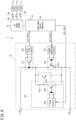
- FIG. 8 is a circuit diagram depicting the interface circuit 29 on the functional control board 2 according to the second example.
- This circuit diagram can be regarded as depicting a basic circuit obtained by further simplifying the circuit depicted in FIG. 5 .
- the circuit configurations other than a switch 296 are similar to circuit configurations on the circuit depicted in FIG. 5 , and are thus denoted by the identical reference signs and will not be described repeatedly.
- the switch 296 is opened when ACS_THRU has the H level, and is closed when ACS_THRU has the L level to short-circuit the phototransistor 293d of the photocoupler 293 and invalidate ACS_OUTPUT.
- Examples of the switch 296 include a semiconductor switch, as well as a relay. Electric resistance is smaller when the switch 296 is constituted by the relay in comparison to the case where the switch 296 is constituted by the semiconductor switch, to inhibit attenuation in signal level of the communication circuit 6 ( FIG. 4 ).
- FIG. 9 is a circuit diagram depicting the interface circuit 29 on the functional control board 2 according to the third example.
- the circuit includes the same constituent components of the circuit depicted in FIG. 5 , and the respective constituent components are thus denoted by the identical reference signs and will not be described repeatedly.
- FIG. 9 is different from FIG. 5 in that the photocoupler 291 has an anode connected with a collector of the transistor 295d and the resistance 295c.
- the bypass circuit 295 operates similarly to the case depicted in FIG. 5 .
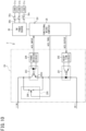
- FIG. 10 is a circuit diagram depicting the interface circuit 29 on the functional control board 2 according to the fourth example.
- the circuit includes the same constituent components of the circuit depicted in FIG. 8 , and the respective constituent components are thus denoted by the identical reference signs and will not be described repeatedly.
- FIG. 10 is different from FIG. 8 in that the photocoupler 291 and the photocoupler 293 are inverted in vertical relation, but the circuit depicted in FIG. 10 operates similarly to the circuit depicted in FIG. 8 .
- the interface circuits according to the above examples may be appropriately combined with each other.
- the interface circuit can have other variations.
- the interface circuit has only to constitute a bypass circuit configured to validate and invalidate ACS_OUTPUT for the functional microcomputer.
- This control device 50 includes the first control board (basic control board 1) connected with the AC power source 3 and equipped with the first control unit (basic microcomputer 18), and the second control board (functional control board 2) provided separately and different from the first control board 1 and equipped with the second control unit (functional microcomputer 28).
- the first control board includes the noise filter 11, the AC-DC converter 14 configured to generate DC voltage from supplied AC voltage, and the DC output wiring 4 configured to allow the DC voltage to be used in the board and also supply the DC voltage to outside the board.
- the second control board is supplied with the DC voltage from the DC output wiring 4.
- the second control board can achieve various additional functions.
- the second control board needs neither a noise filter nor an AC-DC converter, so as to achieve reduction in the number of components relevant to a power source circuit. Accordingly, the number of components can be reduced even in a case where a single apparatus is equipped with a plurality of control boards.
- the first control board and the second control board are preferably accommodated in the common case.
- the first control board and the second control board accommodated in the common case are disposed relatively close to each other, so as to inhibit noise generated on the communication circuit configured to execute communication between the first control unit and the second control unit.
- the case mentioned herein corresponds to an outer package portion having maximum size of the device, and does not matter whether or not to have an internal partition.
- the second control board includes the communication circuit configured to execute communication between the first control unit and the second control unit by means of a current signal.
- the communication circuit includes the input unit configured to provide an input signal from the first control board to the second control unit, the output unit connected in series to the input unit and configured to output an output signal from the second control unit to the first control board, and the bypass circuit 295 provided in parallel with the output unit and including the first switch (295d, 296).
- the second control unit closes the first switch when coming into the sleep mode, and opens the first switch when cancelling the sleep mode.
- the first switch is closed to form the bypass circuit configured to invalidate the output unit of the second control unit in the sleep mode.
- the bypass circuit is formed to keep the communication circuit by means of a current signal even in a case where there is another control board provided for an additional function and configured similarly to the second control board.
- the first switch is the semiconductor switch, and the resistance is connected in series on the positive potential side from a control terminal. This case enables inhibition of control current flowing to the semiconductor switch.
- the first switch being closed has electric resistance preferably less than electric resistance of the output unit. In this case, it is possible to inhibit electric current from flowing toward the output unit and cause electric current to reliably flow to the bypass circuit.
- the second control unit (functional microcomputer 28) is configured to control the function of ventilation, humidification, or washing. Such a function can be achieved by the second control unit independently from the first control unit.
- the second control unit is not limitedly configured to achieve the above function, but may alternatively be configured to control a plurality of indoor units provided in multiple connection.
- the second control unit may be configured to control a hot water supply apparatus connected to the outdoor unit. When the outdoor unit is equipped with two or more fans, the second control unit may be configured to control a second and subsequent fans.
- the second control board includes the switching power source 26 to be supplied with DC voltage, and the switching power source 26 has an output side provided with the second switch (30a, 30b, 30c).
- the second control board opens the second switch so as to inhibit unnecessary power consumption.
- the air conditioner includes the control device according to any one described above.
Landscapes
- Engineering & Computer Science (AREA)
- Chemical & Material Sciences (AREA)
- Combustion & Propulsion (AREA)
- Mechanical Engineering (AREA)
- General Engineering & Computer Science (AREA)
- Power Engineering (AREA)
- Human Computer Interaction (AREA)
- Air Conditioning Control Device (AREA)
Abstract
Description
- The present disclosure relates to a control device, and an air conditioner including the control device.
- An air conditioner includes an outdoor unit and an indoor unit each of which typically has a control board equipped with a microcomputer (see
PATENT LITERATURE 1 or the like). The microcomputers on the two control boards are connected via a transmission line, so as to communicate with each other. Along with advanced functionality of air conditioners in recent years, a single outdoor unit may be provided with a plurality of control boards. - PATENT LITERATURE 1:
Japanese Laid-Open Patent Publication No. 2001-41530 - Provision of the plurality of control boards needs a power source circuit for delivery of DC voltage necessary on each of the boards from an external commercial AC power source. This increases the total number of components necessary for the power source circuit.
- In view of this, it is an object of the present disclosure to reduce the number of components even in a case where a single apparatus is equipped with a plurality of control boards.
-
- (1) The present disclosure provides a control device including: a first control board connected with an AC power source and equipped with a first control unit; and a second control board provided separately and different from the first control board and equipped with a second control unit; in which the first control board includes a noise filter, an AC-DC converter configured to generate DC voltage from AC voltage, and DC output wiring configured to allow the DC voltage to be used in the board and also supply the DC voltage to outside the board, and the second control board is supplied with the DC voltage from the DC output wiring.
- In the control device thus configured, the second control board needs neither a noise filter nor an AC-DC converter, so as to achieve reduction in the number of components relevant to a power source circuit. Accordingly, the number of components can be reduced even in a case where a single apparatus is equipped with a plurality of control boards.
- (2)In the control device according to (1) described above, the first control board and the second control board are preferably accommodated in a common case.
- In this case, it is possible to inhibit noise generated on a communication circuit configured to execute communication between the first control unit and the second control unit.
- (3)In the control device according to (1) or (2) described above, for example, the second control board includes a communication circuit configured to execute communication between the first control unit and the second control unit by means of a current signal, and the communication circuit includes an input unit configured to provide an input signal from the first control board to the second control unit, an output unit connected in series to the input unit and configured to output an output signal from the second control unit to the first control board, and a bypass circuit provided in parallel with the output unit and including a first switch, and the second control unit closes the first switch when coming into a sleep mode and opens the first switch when cancelling the sleep mode.
- In this case, the bypass circuit is formed to keep the communication circuit by means of a current signal even in a case where there is another control board provided for an additional function and configured similarly to the second control board.
- (4)In the control device according to (3) described above, the first switch is a semiconductor switch or the like, and resistance is connected in series on a positive potential side from a control terminal.
- This case enables inhibition of control current flowing to the semiconductor switch.
- (5)In the control device according to (3) or (4) described above, when the first switch is closed, electric resistance is less than electric resistance of the output unit.
- Electric current can reliably flow to the bypass circuit in this case.
- (6)In the control device according to (1) to (5) described above, the second control unit exemplarily controls a function of ventilation, humidification, or washing.
- Such a function can be achieved by the second control unit independently from the first control unit.
- (7)In the control device according to any one of (1) to (6) described above, optionally, the second control board includes a switching power source to be supplied with the DC voltage, and the switching power source has an output side provided with a second switch.
- When the second control unit comes into the sleep mode, the second control board opens the second switch so as to inhibit power consumption.
- An air conditioner includes the control device according to (1) to (7) described above.
-
-
FIG. 1 is a diagram depicting exemplary outer appearance of an air conditioner. -
FIG. 2 is a functional schematic view of the air conditioner. -
FIG. 3 is a circuit connection diagram depicting an exemplary center part of a control device in the air conditioner. -
FIG. 4 is a circuit diagram depicting a communication circuit for communication between microcomputers. -
FIG. 5 is a circuit diagram depicting an interface circuit on a functional control board according to a first example. -
FIG. 6 is an exemplary timing chart in a case where a functional microcomputer comes into a sleep mode from a normal mode. -
FIG. 7 is an exemplary timing chart in a case where the functional microcomputer returns into the normal mode from the sleep mode. -
FIG. 8 is a circuit diagram depicting the interface circuit on the functional control board according to a second example. -
FIG. 9 is a circuit diagram depicting the interface circuit on the functional control board according to a third example. -
FIG. 10 is a circuit diagram depicting the interface circuit on the functional control board according to a fourth example. - Description will be made hereinafter to an embodiment of the present disclosure with reference to the drawings.
-
FIG. 1 is a diagram depicting exemplary outer appearance of anair conditioner 100. Theair conditioner 100 includes anoutdoor unit 101 and anindoor unit 102. Theoutdoor unit 101 includes acase 101c constituted by abody unit 101a having a built-in refrigerant circuit, and a ventilating-humidifyingunit 101b provided thereon. Thecase 101c mentioned herein corresponds to an outer package portion having maximum size of theoutdoor unit 101, and does not matter whether or not to have an internal partition. Theoutdoor unit 101 and theindoor unit 102 are connected via arefrigerant pipe 103 and anair pipe 104. -
FIG. 2 is a functional schematic view of theair conditioner 100. Thebody unit 101a of theoutdoor unit 101 includes, in the mentioned order, aliquid shutoff valve 105, afilter 106, anexpansion valve 107, aheat exchanger 108, a four-way switching valve 109, acompressor 110, anaccumulator 111, and agas shutoff valve 112, which constitute a known refrigerant circuit connected as depicted. Theheat exchanger 108 is provided with afan 113 for ventilation. - The
indoor unit 102 includes aheat exchanger 113, an expansion valve 114, and afan 115, which are connected as depicted. Theoutdoor unit 101 and theindoor unit 102 are connected to each other via aliquid refrigerant tube 103L and agas refrigerant tube 103G. - The ventilating-humidifying
unit 101b includes an intake-exhaust fan 120, aheater 121, ahumidifying rotor 122, and anadsorption fan 123. The ventilating-humidifyingunit 101b is configured to discharge outdoors indoor air introduced into theindoor unit 102, and add moisture to fresh outdoor air and send indoors the air thus humidified. In winter, the ventilating-humidifyingunit 101b is configured to introduce indoors air heated with use of theheater 121. The ventilating-humidifyingunit 101b is connected with theindoor unit 102 via theair pipe 104. - The
body unit 101a of theoutdoor unit 101 operates in accordance with an own basic microcomputer to be described later. The ventilating-humidifyingunit 101b operates in accordance with an own functional microcomputer to be described later. -
FIG. 3 is a circuit connection diagram depicting an exemplary center part of acontrol device 50 in theair conditioner 100. This figure depicts control boards each constituted by a printed circuit board. The control boards include a basic control board 1 (first control board) having a control function of achieving basic operation as theair conditioner 100, and a functional control board 2 (second control board) having a control function of achieving an additional function. Thefunctional control board 2 is provided separately and is different from thebasic control board 1. Though the figure depicts the singlefunctional control board 2, there may occasionally be provided a plurality of functional control boards. - The
basic control board 1 is connected with an externalAC power source 3. Thebasic control board 1 is provided thereon with a noise filter 11, an AC-DC converter 14 including arectifier circuit 12 and a smoothingcapacitor 13, aterminal block 15 for external power supply, a switchingpower source 16, a capacitor 17, a basic microcomputer (first control unit) 18, and aninterface circuit 19, which are connected as depicted. - The noise filter 11 inhibits noise leakage from the
basic control board 1 to theAC power source 3. The AC-DC converter 14 rectifies by voltage doubling and smooths AC voltage (e.g. 100 V) to obtain DC voltage (about 280 V). Rectification by voltage doubling is merely exemplary, and the AC-DC converter has only to be a circuit configured to rectify and smooth AC voltage. This DC voltage is stepped down to predetermined voltage by the switchingpower source 16, for supply of stable control voltage to thebasic microcomputer 18. Thebasic microcomputer 18 achieves basic operation as theair conditioner 100 in accordance with software. The software is stored in a memory (not depicted) equipped in thebasic microcomputer 18. - The
functional control board 2 is connected with thebasic control board 1 viaDC output wiring 4. TheDC output wiring 4 supplies thefunctional control board 2 with DC voltage. Thefunctional control board 2 is provided thereon with a switchingpower source 26, acapacitor 27, a functional microcomputer (second control unit) 28, and aninterface circuit 29, which are connected as depicted. - The DC voltage supplied from the
DC output wiring 4 is stepped down to predetermined voltage by the switchingpower source 26, for supply of stable control voltage to thefunctional microcomputer 28. Thefunctional microcomputer 28 achieves additional functional operation as theair conditioner 100 in accordance with software. The software is stored in a memory (not depicted) equipped in thefunctional microcomputer 28. Thebasic microcomputer 18 and thefunctional microcomputer 28 are connected to each other via theinterface circuit 19, atransmission line 5, and theinterface circuit 29, to execute communication between microcomputers. Thefunctional control board 2 is configured to control a function of ventilation, humidification, washing, or the like, independently from thebasic control board 1. - The
control device 50 depicted inFIG. 3 separately includes thebasic control board 1 for achievement of basic functions and thefunctional control board 2 for achievement of additional functions, so as to prepare various additional functions by thefunctional control board 2. Thefunctional control board 2 needs neither a noise filter nor an AC-DC converter, so as to achieve reduction in the number of components relevant to a power source circuit. - The
basic control board 1 and thefunctional control board 2 are both accommodated in thecommon case 101c (FIG. 1 ). The bothcontrol boards interface circuit 19, thetransmission line 5, and the interface circuit 29) configured to execute communication between thebasic microcomputer 18 and thefunctional microcomputer 28. - Description is made next with focus on communication between microcomputers.
FIG. 4 is a circuit diagram depicting acommunication circuit 6 for communication between microcomputers.FIG. 3 exemplifies communication between thebasic microcomputer 18 and thefunctional microcomputer 28 as one-to-one relation, whereasFIG. 4 depicts a case where there are provided two (exemplifying a plurality of) functional control boards. Similarly to thefunctional control board 2, an additionalfunctional control board 2x includes afunctional microcomputer 28x and aninterface circuit 29x. - The
communication circuit 6 is provided as a closed circuit configured to cause a current signal to flow in a time dividing manner. Thecommunication circuit 6 constituted by theinterface circuits -
FIG. 5 is a circuit diagram depicting theinterface circuit 29 on thefunctional control board 2 according to the first example. InFIG. 5 , theinterface circuit 29 includes aphotocoupler 291 functioning as an input unit for a signal transmitted from thebasic microcomputer 18, areception circuit 292, aphotocoupler 293 functioning as an output unit for a signal to be transmitted to thebasic microcomputer 18, atransmission circuit 294, and a bypass circuit (also called an ACS through circuit) 295. Thebypass circuit 295 is configured to short-circuit and invalidate both ends of theoutput unit 293 in the sleep mode. - When a current signal flows to the
photocoupler 291, an input signal ACS_INPUT is provided to thefunctional microcomputer 28 via thereception circuit 292. Thefunctional microcomputer 28 outputs an output signal ACS_OUTPUT that turns ON or OFF thephotocoupler 293 via thetransmission circuit 294. - The
bypass circuit 295 is constituted by adrive circuit 295a, aphotocoupler 295b,resistance 295c, and atransistor 295d, which are connected as depicted. Examples of theresistance 295c has high resistance of about 24 kS2. An ACS_THRU signal has an H level when thefunctional microcomputer 28 is in the normal mode (operating at high speed), and has an L level when thefunctional microcomputer 28 is in the sleep mode (operating at low speed). - When the ACS _THRU signal has the H level, the
drive circuit 295a turns ON thephotocoupler 295b. In this case, thetransistor 295d is in an OFF state because thetransistor 295d has no voltage generated between a base and an emitter, and the communication circuit 6 (FIG. 4 ) has electric current flowing through thephotocoupler 293. In other words, thephotocoupler 293 is ready to output a signal. In this case, thebypass circuit 295 has electric current flowing from theresistance 295c and passing thephotocoupler 295b. The electric current is quite small because theresistance 295c has a high resistance value. - When the ACS_THRU signal has the L level, the
drive circuit 295a turns OFF thephotocoupler 295b. In this case, thetransistor 295d is in an ON state because thetransistor 295d has voltage applied between the base and the emitter via theresistance 295c. Thephotocoupler 293 is bypassed by thetransistor 295d connected in parallel, and thephotocoupler 293 includes aphototransistor 293d being short-circuited. Thefunctional microcomputer 28 has an output port (a port for ACS_OUTPUT) thus invalidated. - The switching
power source 26 supplies power to a device other than thefunctional microcomputer 28, and exemplarily supplies voltage of 5 V to aload 31a via aswitch 30a. Similarly, the switchingpower source 26 supplies voltage of 14 V to aload 31b via aswitch 30b, and supplies voltage of 15 V to aload 31c via aswitch 30c. Thefunctional microcomputer 28 is configured to control to turn ON or OFF theswitches output port 281. -
FIG. 6 is an exemplary timing chart in a case where thefunctional microcomputer 28 comes into the sleep mode from the normal mode. The timing chart indicates, in the mentioned order from the top, ACS_OUTPUT, ACS_INPUT, ACS_THRU, a port state, a load off port (5 V, 14 V, 15 V), and a microcomputer operation mode. The port state indicates whether the output port (the port for ACS_OUTPUT) is valid or invalid. When the port state is invalid, an input port is also invalid except for microcomputer reset and ACS_INPUT. The load off port corresponds to theoutput port 281. - In an initial state, communication is executed between the
basic microcomputer 18 and thefunctional microcomputer 28. ACS_THRU has the H level, and the port for ACS_OUTPUT is valid. The load off port also has the H level, and theswitches - At time t1, a signal inquiring about authorization for switching into the sleep mode is transmitted from the
functional microcomputer 28 to thebasic microcomputer 18. At time t2, thebasic microcomputer 18 transmits, to thefunctional microcomputer 28, a signal authorizing to switch into the sleep mode. Communication between microcomputers is stopped hereafter. At time t3, ACS_THRU changes to the L level. At time t4, thetransistor 295d (FIG. 5 ) is turned ON, and the port state for ACS_OUTPUT becomes invalid. At time t5, the load off port has the L level, and power supply to theloads functional microcomputer 28 having come into the sleep mode opens theswitches - In this manner, when the function of the
functional control board 2 is not in use, thetransistor 295d (FIG. 5 ) is turned ON (closed) to form bypass wiring at an output unit of thefunctional microcomputer 28 in the sleep mode. The output unit is thus invalidated. The bypass wiring is formed to keep the communication circuit for communication between microcomputers by means of a current signal even in a case where there is another functional control board provided for an additional function. Theresistance 295c provided in series on a positive potential side of the base of thetransistor 295d has high resistance (e.g. 24 kS2), so as to inhibit electric current flowing to thetransistor 295d through theresistance 295c in the sleep mode. - The
transistor 295d inFIG. 5 has ON resistance (electric resistance) less than ON resistance of thephotocoupler 293. It is thus possible to inhibit electric current from flowing toward thephotocoupler 293 and cause electric current to reliably flow to thetransistor 295d on thebypass circuit 295. -
FIG. 7 is an exemplary timing chart in a case where thefunctional microcomputer 28 returns into the normal mode from the sleep mode. Similarly toFIG. 5 , the timing chart indicates, in the mentioned order from the top, ACS_OUTPUT, ACS_INPUT, ACS_THRU, the port state, the load off port, and the microcomputer operation mode. - The
basic microcomputer 18 transmits a signal for cancellation of the sleep mode. At the time 11, thefunctional microcomputer 28 having received the signal for cancellation of the sleep mode changes the microcomputer operation mode from the sleep mode into the normal mode. At the time t2, the load off port changes to the H level, and power supply to theloads functional microcomputer 28 becomes valid. At the time t4, ACS_THRU reaches the H level. At the time t5, thefunctional microcomputer 28 notifies thebasic microcomputer 18 of return into the normal mode, to enable communication between microcomputers hereafter. - Exemplifies below are variations of the interface circuit on the functional control board.
-
FIG. 8 is a circuit diagram depicting theinterface circuit 29 on thefunctional control board 2 according to the second example. This circuit diagram can be regarded as depicting a basic circuit obtained by further simplifying the circuit depicted inFIG. 5 . The circuit configurations other than aswitch 296 are similar to circuit configurations on the circuit depicted inFIG. 5 , and are thus denoted by the identical reference signs and will not be described repeatedly. Theswitch 296 is opened when ACS_THRU has the H level, and is closed when ACS_THRU has the L level to short-circuit thephototransistor 293d of thephotocoupler 293 and invalidate ACS_OUTPUT. Examples of theswitch 296 include a semiconductor switch, as well as a relay. Electric resistance is smaller when theswitch 296 is constituted by the relay in comparison to the case where theswitch 296 is constituted by the semiconductor switch, to inhibit attenuation in signal level of the communication circuit 6 (FIG. 4 ). -
FIG. 9 is a circuit diagram depicting theinterface circuit 29 on thefunctional control board 2 according to the third example. The circuit includes the same constituent components of the circuit depicted inFIG. 5 , and the respective constituent components are thus denoted by the identical reference signs and will not be described repeatedly.FIG. 9 is different fromFIG. 5 in that thephotocoupler 291 has an anode connected with a collector of thetransistor 295d and theresistance 295c. Thebypass circuit 295 operates similarly to the case depicted inFIG. 5 . -
FIG. 10 is a circuit diagram depicting theinterface circuit 29 on thefunctional control board 2 according to the fourth example. The circuit includes the same constituent components of the circuit depicted inFIG. 8 , and the respective constituent components are thus denoted by the identical reference signs and will not be described repeatedly.FIG. 10 is different fromFIG. 8 in that thephotocoupler 291 and thephotocoupler 293 are inverted in vertical relation, but the circuit depicted inFIG. 10 operates similarly to the circuit depicted inFIG. 8 . - At least part of the interface circuits according to the above examples may be appropriately combined with each other. The interface circuit can have other variations. In short, the interface circuit has only to constitute a bypass circuit configured to validate and invalidate ACS_OUTPUT for the functional microcomputer.
- The above disclosure can be expressed generally as follows.
- This
control device 50 includes the first control board (basic control board 1) connected with theAC power source 3 and equipped with the first control unit (basic microcomputer 18), and the second control board (functional control board 2) provided separately and different from thefirst control board 1 and equipped with the second control unit (functional microcomputer 28). The first control board includes the noise filter 11, the AC-DC converter 14 configured to generate DC voltage from supplied AC voltage, and theDC output wiring 4 configured to allow the DC voltage to be used in the board and also supply the DC voltage to outside the board. The second control board is supplied with the DC voltage from theDC output wiring 4. - In an exemplary case where the
control device 50 thus configured includes the first control board for achievement of the basic functions of the device and the second control board for achievement of the additional functions of the device, the second control board can achieve various additional functions. The second control board needs neither a noise filter nor an AC-DC converter, so as to achieve reduction in the number of components relevant to a power source circuit. Accordingly, the number of components can be reduced even in a case where a single apparatus is equipped with a plurality of control boards. - The first control board and the second control board are preferably accommodated in the common case.
- The first control board and the second control board accommodated in the common case are disposed relatively close to each other, so as to inhibit noise generated on the communication circuit configured to execute communication between the first control unit and the second control unit. The case mentioned herein corresponds to an outer package portion having maximum size of the device, and does not matter whether or not to have an internal partition.
- The second control board includes the communication circuit configured to execute communication between the first control unit and the second control unit by means of a current signal. The communication circuit includes the input unit configured to provide an input signal from the first control board to the second control unit, the output unit connected in series to the input unit and configured to output an output signal from the second control unit to the first control board, and the
bypass circuit 295 provided in parallel with the output unit and including the first switch (295d, 296). The second control unit closes the first switch when coming into the sleep mode, and opens the first switch when cancelling the sleep mode. - In this case, when the function of the second control board is not in use, the first switch is closed to form the bypass circuit configured to invalidate the output unit of the second control unit in the sleep mode. The bypass circuit is formed to keep the communication circuit by means of a current signal even in a case where there is another control board provided for an additional function and configured similarly to the second control board.
- The first switch is the semiconductor switch, and the resistance is connected in series on the positive potential side from a control terminal. This case enables inhibition of control current flowing to the semiconductor switch.
- The first switch being closed has electric resistance preferably less than electric resistance of the output unit. In this case, it is possible to inhibit electric current from flowing toward the output unit and cause electric current to reliably flow to the bypass circuit.
- The second control unit (functional microcomputer 28) is configured to control the function of ventilation, humidification, or washing. Such a function can be achieved by the second control unit independently from the first control unit. The second control unit is not limitedly configured to achieve the above function, but may alternatively be configured to control a plurality of indoor units provided in multiple connection. The second control unit may be configured to control a hot water supply apparatus connected to the outdoor unit. When the outdoor unit is equipped with two or more fans, the second control unit may be configured to control a second and subsequent fans.
- The second control board includes the switching
power source 26 to be supplied with DC voltage, and the switchingpower source 26 has an output side provided with the second switch (30a, 30b, 30c). - When the second control unit comes into the sleep mode, the second control board opens the second switch so as to inhibit unnecessary power consumption.
- The air conditioner includes the control device according to any one described above.
- The embodiment has been described above. Various modifications to modes and details should be available without departing from the object and the scope of the claims.
-
- 1
- basic control board (first control board)
- 2
- functional control board (second control board)
- 3
- AC power source
- 4
- DC output wiring
- 5
- transmission line
- 6
- communication circuit
- 11
- noise filter
- 12
- rectifier circuit
- 13
- smoothing capacitor
- 14
- AC-DC converter
- 15
- terminal block
- 16
- switching power source
- 17
- capacitor
- 18
- basic microcomputer (first control unit)
- 19
- interface circuit
- 26
- switching power source
- 27
- capacitor
- 28
- functional microcomputer (second control unit)
- 29, 29x
- interface circuit
- 30a, 30b, 30c
- switch (second switch)
- 31a, 31b, 31c
- load
- 50
- control device
- 100
- air conditioner
- 101
- outdoor unit
- 101a
- body unit
- 101b
- ventilating-humidifying unit
- 101c
- case
- 102
- indoor unit
- 103
- refrigerant pipe
- 103L
- liquid refrigerant tube
- 103G
- gas refrigerant tube
- 104
- air pipe
- 105
- liquid shutoff valve
- 106
- filter
- 107
- expansion valve
- 108
- heat exchanger
- 109
- four-way switching valve
- 110
- compressor
- 111
- accumulator
- 112
- gas shutoff valve
- 113
- heat exchanger
- 114
- expansion valve
- 115
- fan
- 120
- fan
- 121
- heater
- 122
- humidifying rotor
- 123
- adsorption fan
- 281
- output port (load off port)
- 291
- photocoupler (input unit)
- 292
- reception circuit
- 293
- photocoupler (output unit)
- 293d
- phototransistor
- 294
- transmission circuit
- 295
- bypass circuit
- 295a
- drive circuit
- 295b
- photocoupler
- 295c
- resistance
- 295d
- transistor (first switch)
- 296
- switch (first switch)
Claims (8)
- A control device comprising:a first control board (1) connected with an AC power source (3) and equipped with a first control unit (18); anda second control board (2) provided separately and different from the first control board (1) and equipped with a second control unit (28); whereinthe first control board (1) includes a noise filter (11), an AC-DC converter (14) configured to generate DC voltage from AC voltage, and DC output wiring (4) configured to allow the DC voltage to be used in the board and also supply the DC voltage to outside the board, andthe second control board (2) is supplied with the DC voltage from the DC output wiring (4).
- The control device according to claim 1, wherein the first control board (1) and the second control board (2) are accommodated in a common case (101c).
- The control device according to claim 1 or 2, whereinthe second control board (2) includes a communication circuit (6) configured to execute communication between the first control unit (18) and the second control unit (28) by means of a current signal, and the communication circuit (6) includesan input unit (291) configured to provide an input signal from the first control board (1) to the second control unit (28),an output unit (293) connected in series to the input unit (291) and configured to output an output signal from the second control unit (28) to the first control board (1), anda bypass circuit (295) provided in parallel with the output unit (293) and including a first switch (295d, 296), andthe second control unit (28) closes the first switch (295d, 296) when coming into a sleep mode and opens the first switch (295d, 296) when cancelling the sleep mode.
- The control device according to claim 3, wherein the first switch (295d) is a semiconductor switch, and resistance (295c) is connected in series on a positive potential side from a control terminal.
- The control device according to claim 3 or 4, wherein, when the first switch (295d, 296) is closed, electric resistance is less than electric resistance of the output unit (293).
- The control device according to any one of claims 1 to 5, wherein the second control unit (28) controls a function of ventilation, humidification, or washing.
- The control device according to any one of claims 1 to 6, whereinthe second control board (2) includes a switching power source (26) to be supplied with the DC voltage, andthe switching power source (26) has an output side provided with a second switch (30a, 30b, 30c).
- An air conditioner comprising the control device according to any one of claims 1 to 7.
Applications Claiming Priority (2)
| Application Number | Priority Date | Filing Date | Title |
|---|---|---|---|
| JP2021172869A JP7393674B2 (en) | 2021-10-22 | 2021-10-22 | Control equipment and air conditioning equipment |
| PCT/JP2022/039239 WO2023068358A1 (en) | 2021-10-22 | 2022-10-21 | Control device and air conditioning device |
Publications (3)
| Publication Number | Publication Date |
|---|---|
| EP4421398A1 true EP4421398A1 (en) | 2024-08-28 |
| EP4421398A4 EP4421398A4 (en) | 2024-12-25 |
| EP4421398B1 EP4421398B1 (en) | 2025-08-13 |
Family
ID=86058315
Family Applications (1)
| Application Number | Title | Priority Date | Filing Date |
|---|---|---|---|
| EP22883661.5A Active EP4421398B1 (en) | 2021-10-22 | 2022-10-21 | Control device and air conditioning device |
Country Status (6)
| Country | Link |
|---|---|
| US (1) | US20240191904A1 (en) |
| EP (1) | EP4421398B1 (en) |
| JP (1) | JP7393674B2 (en) |
| CN (1) | CN118140097B (en) |
| ES (1) | ES3041819T3 (en) |
| WO (1) | WO2023068358A1 (en) |
Families Citing this family (1)
| Publication number | Priority date | Publication date | Assignee | Title |
|---|---|---|---|---|
| JP7853607B2 (en) | 2024-10-07 | 2026-04-30 | ダイキン工業株式会社 | Electrical component modules and air conditioning systems |
Family Cites Families (17)
| Publication number | Priority date | Publication date | Assignee | Title |
|---|---|---|---|---|
| JP3991425B2 (en) * | 1998-03-11 | 2007-10-17 | ダイキン工業株式会社 | Air conditioner outdoor unit |
| JP3613752B2 (en) | 1999-01-21 | 2005-01-26 | 松下電器産業株式会社 | Electronic control device |
| JP3263675B2 (en) * | 1999-02-02 | 2002-03-04 | 三洋電機株式会社 | Electronic devices with common connectors |
| JP3518433B2 (en) | 1999-07-29 | 2004-04-12 | ダイキン工業株式会社 | Air conditioner |
| CN1227486C (en) * | 2000-04-24 | 2005-11-16 | 三洋电机株式会社 | Communication system of air conditioner |
| JP3564525B2 (en) | 2000-09-12 | 2004-09-15 | ダイキン工業株式会社 | Air conditioner |
| JP4179794B2 (en) * | 2002-04-30 | 2008-11-12 | 三洋電機株式会社 | Outdoor unit and air conditioning system |
| KR101564727B1 (en) | 2007-12-21 | 2015-10-30 | 엘지전자 주식회사 | air conditioner |
| KR101438910B1 (en) * | 2012-10-04 | 2014-09-11 | 엘지이노텍 주식회사 | The Wired-Wireless Combined Power Transmission Apparatus and The Method using the same |
| JP6157374B2 (en) * | 2014-02-05 | 2017-07-05 | 三菱電機株式会社 | Air conditioner |
| JP6281818B2 (en) * | 2014-04-01 | 2018-02-21 | パナソニックIpマネジメント株式会社 | Management system |
| JP6566711B2 (en) * | 2015-05-08 | 2019-08-28 | 日立ジョンソンコントロールズ空調株式会社 | Air conditioner |
| US10581274B2 (en) * | 2015-06-03 | 2020-03-03 | Lg Electronics Inc. | Home appliance |
| KR102549128B1 (en) * | 2016-12-21 | 2023-06-29 | 삼성전자주식회사 | Air conditioning apparatus, central control apparatus of the air conditioning apparatus, remote control apparatus of the air conditioning apparatus, indoor appratus of the air conditioning apparatus and method of controlling thereof |
| EP3611438B1 (en) * | 2017-04-10 | 2023-01-04 | Mitsubishi Electric Corporation | Air conditioning ventilation device and control method |
| EP3933290B1 (en) * | 2019-02-26 | 2024-07-24 | Mitsubishi Electric Corporation | Electrical device |
| JP7587922B2 (en) * | 2020-01-20 | 2024-11-21 | ダイキン インダストリーズ (タイランド) リミテッド | Electrical board and refrigeration device equipped with said electric board |
-
2021
- 2021-10-22 JP JP2021172869A patent/JP7393674B2/en active Active
-
2022
- 2022-10-21 ES ES22883661T patent/ES3041819T3/en active Active
- 2022-10-21 EP EP22883661.5A patent/EP4421398B1/en active Active
- 2022-10-21 CN CN202280070667.1A patent/CN118140097B/en active Active
- 2022-10-21 WO PCT/JP2022/039239 patent/WO2023068358A1/en not_active Ceased
-
2024
- 2024-02-22 US US18/584,042 patent/US20240191904A1/en active Pending
Also Published As
| Publication number | Publication date |
|---|---|
| JP7393674B2 (en) | 2023-12-07 |
| WO2023068358A1 (en) | 2023-04-27 |
| EP4421398A4 (en) | 2024-12-25 |
| US20240191904A1 (en) | 2024-06-13 |
| EP4421398B1 (en) | 2025-08-13 |
| CN118140097B (en) | 2024-12-03 |
| ES3041819T3 (en) | 2025-11-14 |
| JP2023062775A (en) | 2023-05-09 |
| CN118140097A (en) | 2024-06-04 |
Similar Documents
| Publication | Publication Date | Title |
|---|---|---|
| US12359839B2 (en) | Control circuit for air conditioner outdoor unit, electric control component and air conditioner | |
| US20080203866A1 (en) | Rooftop modular fan coil unit | |
| ES2561166T3 (en) | Air conditioner | |
| EP4421398B1 (en) | Control device and air conditioning device | |
| CN101237215B (en) | Car air-conditioner frequency conversion control system and its method | |
| US10203141B1 (en) | Multi-stage compressor with variable speed drive and method of use | |
| CN207015110U (en) | an air conditioning system | |
| CN107187292B (en) | An air conditioning system and its control method | |
| CN212457525U (en) | Throttling device, refrigerant circulation system and dehumidifier | |
| CN203404923U (en) | Total-heat-recovery-type folding air sending-returning-discharging-integrated air conditioning unit | |
| CN216481670U (en) | Modular multi-split system | |
| CN110500696A (en) | A kind of control circuit and air-conditioning | |
| CN206094344U (en) | Air condensing units and have its air conditioner | |
| JP3059926B2 (en) | Air conditioner | |
| CN212431388U (en) | Three-pipe temperature and humidity balance air conditioning system | |
| KR102295972B1 (en) | Air conditioner | |
| CN211233112U (en) | Air conditioning system | |
| CN209165781U (en) | The heat pump air-heater efficiently heated | |
| CN223401178U (en) | Heat pump SPA integrated control device and integrated equipment | |
| CN111351150A (en) | Heat pump heat recovery type water-wind integrated unit | |
| CN217785343U (en) | Double-compressor type multi-connected indoor climate control system | |
| CN204901992U (en) | Split standard type air -conditioner | |
| CN223925164U (en) | A compact air conditioning unit evaporator assembly with condensing reheat function | |
| CN217441826U (en) | Outdoor unit and air conditioner | |
| CN215892615U (en) | Three-in-one system of floor heating, air conditioner and fresh air |
Legal Events
| Date | Code | Title | Description |
|---|---|---|---|
| STAA | Information on the status of an ep patent application or granted ep patent |
Free format text: STATUS: THE INTERNATIONAL PUBLICATION HAS BEEN MADE |
|
| PUAI | Public reference made under article 153(3) epc to a published international application that has entered the european phase |
Free format text: ORIGINAL CODE: 0009012 |
|
| STAA | Information on the status of an ep patent application or granted ep patent |
Free format text: STATUS: REQUEST FOR EXAMINATION WAS MADE |
|
| 17P | Request for examination filed |
Effective date: 20240208 |
|
| AK | Designated contracting states |
Kind code of ref document: A1 Designated state(s): AL AT BE BG CH CY CZ DE DK EE ES FI FR GB GR HR HU IE IS IT LI LT LU LV MC ME MK MT NL NO PL PT RO RS SE SI SK SM TR |
|
| A4 | Supplementary search report drawn up and despatched |
Effective date: 20241122 |
|
| RIC1 | Information provided on ipc code assigned before grant |
Ipc: F24F 3/06 20060101ALI20241118BHEP Ipc: F24F 11/89 20180101ALI20241118BHEP Ipc: F24F 11/88 20180101ALI20241118BHEP Ipc: H02M 1/00 20060101ALI20241118BHEP Ipc: F24F 11/54 20180101ALI20241118BHEP Ipc: F24F 11/63 20180101AFI20241118BHEP |
|
| DAV | Request for validation of the european patent (deleted) | ||
| DAX | Request for extension of the european patent (deleted) | ||
| P01 | Opt-out of the competence of the unified patent court (upc) registered |
Free format text: CASE NUMBER: APP_1056/2025 Effective date: 20250108 |
|
| GRAP | Despatch of communication of intention to grant a patent |
Free format text: ORIGINAL CODE: EPIDOSNIGR1 |
|
| STAA | Information on the status of an ep patent application or granted ep patent |
Free format text: STATUS: GRANT OF PATENT IS INTENDED |
|
| RIC1 | Information provided on ipc code assigned before grant |
Ipc: F24F 3/06 20060101ALI20250411BHEP Ipc: F24F 11/89 20180101ALI20250411BHEP Ipc: F24F 11/88 20180101ALI20250411BHEP Ipc: H02M 1/00 20060101ALI20250411BHEP Ipc: F24F 11/54 20180101ALI20250411BHEP Ipc: F24F 11/63 20180101AFI20250411BHEP |
|
| INTG | Intention to grant announced |
Effective date: 20250429 |
|
| GRAS | Grant fee paid |
Free format text: ORIGINAL CODE: EPIDOSNIGR3 |
|
| GRAA | (expected) grant |
Free format text: ORIGINAL CODE: 0009210 |
|
| STAA | Information on the status of an ep patent application or granted ep patent |
Free format text: STATUS: THE PATENT HAS BEEN GRANTED |
|
| AK | Designated contracting states |
Kind code of ref document: B1 Designated state(s): AL AT BE BG CH CY CZ DE DK EE ES FI FR GB GR HR HU IE IS IT LI LT LU LV MC ME MK MT NL NO PL PT RO RS SE SI SK SM TR |
|
| REG | Reference to a national code |
Ref country code: GB Ref legal event code: FG4D |
|
| REG | Reference to a national code |
Ref country code: CH Ref legal event code: EP |
|
| REG | Reference to a national code |
Ref country code: DE Ref legal event code: R096 Ref document number: 602022019599 Country of ref document: DE |
|
| REG | Reference to a national code |
Ref country code: IE Ref legal event code: FG4D |
|
| REG | Reference to a national code |
Ref country code: ES Ref legal event code: FG2A Ref document number: 3041819 Country of ref document: ES Kind code of ref document: T3 Effective date: 20251114 |
|
| REG | Reference to a national code |
Ref country code: NL Ref legal event code: MP Effective date: 20250813 |
|
| PG25 | Lapsed in a contracting state [announced via postgrant information from national office to epo] |
Ref country code: IS Free format text: LAPSE BECAUSE OF FAILURE TO SUBMIT A TRANSLATION OF THE DESCRIPTION OR TO PAY THE FEE WITHIN THE PRESCRIBED TIME-LIMIT Effective date: 20251213 |
|
| PGFP | Annual fee paid to national office [announced via postgrant information from national office to epo] |
Ref country code: DE Payment date: 20251021 Year of fee payment: 4 |
|
| PG25 | Lapsed in a contracting state [announced via postgrant information from national office to epo] |
Ref country code: NO Free format text: LAPSE BECAUSE OF FAILURE TO SUBMIT A TRANSLATION OF THE DESCRIPTION OR TO PAY THE FEE WITHIN THE PRESCRIBED TIME-LIMIT Effective date: 20251113 |
|
| REG | Reference to a national code |
Ref country code: LT Ref legal event code: MG9D |
|
| PG25 | Lapsed in a contracting state [announced via postgrant information from national office to epo] |
Ref country code: PT Free format text: LAPSE BECAUSE OF FAILURE TO SUBMIT A TRANSLATION OF THE DESCRIPTION OR TO PAY THE FEE WITHIN THE PRESCRIBED TIME-LIMIT Effective date: 20251215 |
|
| PG25 | Lapsed in a contracting state [announced via postgrant information from national office to epo] |
Ref country code: FI Free format text: LAPSE BECAUSE OF FAILURE TO SUBMIT A TRANSLATION OF THE DESCRIPTION OR TO PAY THE FEE WITHIN THE PRESCRIBED TIME-LIMIT Effective date: 20250813 |
|
| PGFP | Annual fee paid to national office [announced via postgrant information from national office to epo] |
Ref country code: IT Payment date: 20251031 Year of fee payment: 4 |
|
| PG25 | Lapsed in a contracting state [announced via postgrant information from national office to epo] |
Ref country code: NL Free format text: LAPSE BECAUSE OF FAILURE TO SUBMIT A TRANSLATION OF THE DESCRIPTION OR TO PAY THE FEE WITHIN THE PRESCRIBED TIME-LIMIT Effective date: 20250813 Ref country code: HR Free format text: LAPSE BECAUSE OF FAILURE TO SUBMIT A TRANSLATION OF THE DESCRIPTION OR TO PAY THE FEE WITHIN THE PRESCRIBED TIME-LIMIT Effective date: 20250813 |
|
| PGFP | Annual fee paid to national office [announced via postgrant information from national office to epo] |
Ref country code: FR Payment date: 20251030 Year of fee payment: 4 |
|
| PG25 | Lapsed in a contracting state [announced via postgrant information from national office to epo] |
Ref country code: GR Free format text: LAPSE BECAUSE OF FAILURE TO SUBMIT A TRANSLATION OF THE DESCRIPTION OR TO PAY THE FEE WITHIN THE PRESCRIBED TIME-LIMIT Effective date: 20251114 |
|
| PG25 | Lapsed in a contracting state [announced via postgrant information from national office to epo] |
Ref country code: SE Free format text: LAPSE BECAUSE OF FAILURE TO SUBMIT A TRANSLATION OF THE DESCRIPTION OR TO PAY THE FEE WITHIN THE PRESCRIBED TIME-LIMIT Effective date: 20250813 |
|
| PG25 | Lapsed in a contracting state [announced via postgrant information from national office to epo] |
Ref country code: LV Free format text: LAPSE BECAUSE OF FAILURE TO SUBMIT A TRANSLATION OF THE DESCRIPTION OR TO PAY THE FEE WITHIN THE PRESCRIBED TIME-LIMIT Effective date: 20250813 |
|
| PG25 | Lapsed in a contracting state [announced via postgrant information from national office to epo] |
Ref country code: PL Free format text: LAPSE BECAUSE OF FAILURE TO SUBMIT A TRANSLATION OF THE DESCRIPTION OR TO PAY THE FEE WITHIN THE PRESCRIBED TIME-LIMIT Effective date: 20250813 Ref country code: BG Free format text: LAPSE BECAUSE OF FAILURE TO SUBMIT A TRANSLATION OF THE DESCRIPTION OR TO PAY THE FEE WITHIN THE PRESCRIBED TIME-LIMIT Effective date: 20250813 |
|
| PG25 | Lapsed in a contracting state [announced via postgrant information from national office to epo] |
Ref country code: RS Free format text: LAPSE BECAUSE OF FAILURE TO SUBMIT A TRANSLATION OF THE DESCRIPTION OR TO PAY THE FEE WITHIN THE PRESCRIBED TIME-LIMIT Effective date: 20251113 |
|
| PGFP | Annual fee paid to national office [announced via postgrant information from national office to epo] |
Ref country code: ES Payment date: 20251217 Year of fee payment: 4 |
|
| REG | Reference to a national code |
Ref country code: AT Ref legal event code: MK05 Ref document number: 1825020 Country of ref document: AT Kind code of ref document: T Effective date: 20250813 |
|
| PG25 | Lapsed in a contracting state [announced via postgrant information from national office to epo] |
Ref country code: RO Free format text: LAPSE BECAUSE OF FAILURE TO SUBMIT A TRANSLATION OF THE DESCRIPTION OR TO PAY THE FEE WITHIN THE PRESCRIBED TIME-LIMIT Effective date: 20250813 |
|
| PG25 | Lapsed in a contracting state [announced via postgrant information from national office to epo] |
Ref country code: SM Free format text: LAPSE BECAUSE OF FAILURE TO SUBMIT A TRANSLATION OF THE DESCRIPTION OR TO PAY THE FEE WITHIN THE PRESCRIBED TIME-LIMIT Effective date: 20250813 |
|
| PG25 | Lapsed in a contracting state [announced via postgrant information from national office to epo] |
Ref country code: DK Free format text: LAPSE BECAUSE OF FAILURE TO SUBMIT A TRANSLATION OF THE DESCRIPTION OR TO PAY THE FEE WITHIN THE PRESCRIBED TIME-LIMIT Effective date: 20250813 |
|
| PG25 | Lapsed in a contracting state [announced via postgrant information from national office to epo] |
Ref country code: AT Free format text: LAPSE BECAUSE OF FAILURE TO SUBMIT A TRANSLATION OF THE DESCRIPTION OR TO PAY THE FEE WITHIN THE PRESCRIBED TIME-LIMIT Effective date: 20250813 |
|
| PG25 | Lapsed in a contracting state [announced via postgrant information from national office to epo] |
Ref country code: CZ Free format text: LAPSE BECAUSE OF FAILURE TO SUBMIT A TRANSLATION OF THE DESCRIPTION OR TO PAY THE FEE WITHIN THE PRESCRIBED TIME-LIMIT Effective date: 20250813 |
|
| PG25 | Lapsed in a contracting state [announced via postgrant information from national office to epo] |
Ref country code: EE Free format text: LAPSE BECAUSE OF FAILURE TO SUBMIT A TRANSLATION OF THE DESCRIPTION OR TO PAY THE FEE WITHIN THE PRESCRIBED TIME-LIMIT Effective date: 20250813 Ref country code: SK Free format text: LAPSE BECAUSE OF FAILURE TO SUBMIT A TRANSLATION OF THE DESCRIPTION OR TO PAY THE FEE WITHIN THE PRESCRIBED TIME-LIMIT Effective date: 20250813 |
|
| REG | Reference to a national code |
Ref country code: DE Ref legal event code: R097 Ref document number: 602022019599 Country of ref document: DE |
|
| REG | Reference to a national code |
Ref country code: CH Ref legal event code: H13 Free format text: ST27 STATUS EVENT CODE: U-0-0-H10-H13 (AS PROVIDED BY THE NATIONAL OFFICE) Effective date: 20260527 |
|
| PG25 | Lapsed in a contracting state [announced via postgrant information from national office to epo] |
Ref country code: LU Free format text: LAPSE BECAUSE OF NON-PAYMENT OF DUE FEES Effective date: 20251021 |
|
| PLBE | No opposition filed within time limit |
Free format text: ORIGINAL CODE: 0009261 |
|
| STAA | Information on the status of an ep patent application or granted ep patent |
Free format text: STATUS: NO OPPOSITION FILED WITHIN TIME LIMIT |
|
| REG | Reference to a national code |
Ref country code: BE Ref legal event code: MM Effective date: 20251031 |
|
| REG | Reference to a national code |
Ref country code: CH Ref legal event code: L10 Free format text: ST27 STATUS EVENT CODE: U-0-0-L10-L00 (AS PROVIDED BY THE NATIONAL OFFICE) Effective date: 20260624 |
|
| PG25 | Lapsed in a contracting state [announced via postgrant information from national office to epo] |
Ref country code: LT Free format text: LAPSE BECAUSE OF FAILURE TO SUBMIT A TRANSLATION OF THE DESCRIPTION OR TO PAY THE FEE WITHIN THE PRESCRIBED TIME-LIMIT Effective date: 20250813 Ref country code: MC Free format text: LAPSE BECAUSE OF FAILURE TO SUBMIT A TRANSLATION OF THE DESCRIPTION OR TO PAY THE FEE WITHIN THE PRESCRIBED TIME-LIMIT Effective date: 20250813 |
|
| PG25 | Lapsed in a contracting state [announced via postgrant information from national office to epo] |
Ref country code: CH Free format text: LAPSE BECAUSE OF NON-PAYMENT OF DUE FEES Effective date: 20251031 Ref country code: BE Free format text: LAPSE BECAUSE OF NON-PAYMENT OF DUE FEES Effective date: 20251031 |
|
| 26N | No opposition filed |
Effective date: 20260515 |