EP4418334A1 - Led device formation using releasable inorganic wafer bond - Google Patents
Led device formation using releasable inorganic wafer bond Download PDFInfo
- Publication number
- EP4418334A1 EP4418334A1 EP24157873.1A EP24157873A EP4418334A1 EP 4418334 A1 EP4418334 A1 EP 4418334A1 EP 24157873 A EP24157873 A EP 24157873A EP 4418334 A1 EP4418334 A1 EP 4418334A1
- Authority
- EP
- European Patent Office
- Prior art keywords
- layer
- wafer
- transparent support
- inorganic
- support wafer
- Prior art date
- Legal status (The legal status is an assumption and is not a legal conclusion. Google has not performed a legal analysis and makes no representation as to the accuracy of the status listed.)
- Pending
Links
- 230000015572 biosynthetic process Effects 0.000 title description 2
- 238000000034 method Methods 0.000 claims abstract description 107
- 238000012545 processing Methods 0.000 claims abstract description 71
- 238000004519 manufacturing process Methods 0.000 claims abstract description 15
- 238000000151 deposition Methods 0.000 claims description 18
- JMASRVWKEDWRBT-UHFFFAOYSA-N Gallium nitride Chemical compound [Ga]#N JMASRVWKEDWRBT-UHFFFAOYSA-N 0.000 claims description 17
- 229910052814 silicon oxide Inorganic materials 0.000 claims description 13
- VYPSYNLAJGMNEJ-UHFFFAOYSA-N Silicium dioxide Chemical compound O=[Si]=O VYPSYNLAJGMNEJ-UHFFFAOYSA-N 0.000 claims description 12
- 229910052594 sapphire Inorganic materials 0.000 claims description 10
- 239000010980 sapphire Substances 0.000 claims description 10
- 229910002601 GaN Inorganic materials 0.000 claims description 9
- 239000011521 glass Substances 0.000 claims description 8
- AJGDITRVXRPLBY-UHFFFAOYSA-N aluminum indium Chemical compound [Al].[In] AJGDITRVXRPLBY-UHFFFAOYSA-N 0.000 claims description 6
- AMGQUBHHOARCQH-UHFFFAOYSA-N indium;oxotin Chemical compound [In].[Sn]=O AMGQUBHHOARCQH-UHFFFAOYSA-N 0.000 claims description 6
- HBMJWWWQQXIZIP-UHFFFAOYSA-N silicon carbide Chemical compound [Si+]#[C-] HBMJWWWQQXIZIP-UHFFFAOYSA-N 0.000 claims description 6
- 229910010271 silicon carbide Inorganic materials 0.000 claims description 6
- 235000012431 wafers Nutrition 0.000 description 219
- 239000000758 substrate Substances 0.000 description 26
- 239000000463 material Substances 0.000 description 25
- 239000004065 semiconductor Substances 0.000 description 13
- 229910052751 metal Chemical group 0.000 description 11
- 239000002184 metal Chemical group 0.000 description 9
- 239000010408 film Substances 0.000 description 7
- 238000005240 physical vapour deposition Methods 0.000 description 7
- 238000000623 plasma-assisted chemical vapour deposition Methods 0.000 description 7
- 239000010936 titanium Substances 0.000 description 6
- XUIMIQQOPSSXEZ-UHFFFAOYSA-N Silicon Chemical compound [Si] XUIMIQQOPSSXEZ-UHFFFAOYSA-N 0.000 description 5
- 229910052710 silicon Inorganic materials 0.000 description 5
- 239000010703 silicon Substances 0.000 description 5
- RTAQQCXQSZGOHL-UHFFFAOYSA-N Titanium Chemical compound [Ti] RTAQQCXQSZGOHL-UHFFFAOYSA-N 0.000 description 4
- 238000000231 atomic layer deposition Methods 0.000 description 4
- 239000011368 organic material Substances 0.000 description 4
- 238000005498 polishing Methods 0.000 description 4
- 229910052719 titanium Inorganic materials 0.000 description 4
- JBRZTFJDHDCESZ-UHFFFAOYSA-N AsGa Chemical compound [As]#[Ga] JBRZTFJDHDCESZ-UHFFFAOYSA-N 0.000 description 3
- 229910045601 alloy Inorganic materials 0.000 description 3
- 239000000956 alloy Substances 0.000 description 3
- 238000005229 chemical vapour deposition Methods 0.000 description 3
- 150000001875 compounds Chemical class 0.000 description 3
- 230000008020 evaporation Effects 0.000 description 3
- 238000001704 evaporation Methods 0.000 description 3
- 230000001737 promoting effect Effects 0.000 description 3
- 229910001218 Gallium arsenide Inorganic materials 0.000 description 2
- 229910001092 metal group alloy Inorganic materials 0.000 description 2
- 238000012986 modification Methods 0.000 description 2
- 230000004048 modification Effects 0.000 description 2
- 230000001590 oxidative effect Effects 0.000 description 2
- TWNQGVIAIRXVLR-UHFFFAOYSA-N oxo(oxoalumanyloxy)alumane Chemical compound O=[Al]O[Al]=O TWNQGVIAIRXVLR-UHFFFAOYSA-N 0.000 description 2
- 230000005855 radiation Effects 0.000 description 2
- 238000000926 separation method Methods 0.000 description 2
- 238000004544 sputter deposition Methods 0.000 description 2
- 239000010409 thin film Substances 0.000 description 2
- 238000007740 vapor deposition Methods 0.000 description 2
- IJGRMHOSHXDMSA-UHFFFAOYSA-N Atomic nitrogen Chemical compound N#N IJGRMHOSHXDMSA-UHFFFAOYSA-N 0.000 description 1
- OKTJSMMVPCPJKN-UHFFFAOYSA-N Carbon Chemical compound [C] OKTJSMMVPCPJKN-UHFFFAOYSA-N 0.000 description 1
- GYHNNYVSQQEPJS-UHFFFAOYSA-N Gallium Chemical compound [Ga] GYHNNYVSQQEPJS-UHFFFAOYSA-N 0.000 description 1
- 229910052581 Si3N4 Inorganic materials 0.000 description 1
- 229910021417 amorphous silicon Inorganic materials 0.000 description 1
- 239000003990 capacitor Substances 0.000 description 1
- 229910052799 carbon Inorganic materials 0.000 description 1
- 239000004020 conductor Substances 0.000 description 1
- 239000000470 constituent Substances 0.000 description 1
- 238000010276 construction Methods 0.000 description 1
- 239000000356 contaminant Substances 0.000 description 1
- 230000032798 delamination Effects 0.000 description 1
- 238000010494 dissociation reaction Methods 0.000 description 1
- 230000005593 dissociations Effects 0.000 description 1
- 238000000407 epitaxy Methods 0.000 description 1
- 239000012467 final product Substances 0.000 description 1
- 229910052733 gallium Inorganic materials 0.000 description 1
- 229910052732 germanium Inorganic materials 0.000 description 1
- GNPVGFCGXDBREM-UHFFFAOYSA-N germanium atom Chemical compound [Ge] GNPVGFCGXDBREM-UHFFFAOYSA-N 0.000 description 1
- 229910052737 gold Inorganic materials 0.000 description 1
- 238000000227 grinding Methods 0.000 description 1
- 238000010438 heat treatment Methods 0.000 description 1
- 229910052738 indium Inorganic materials 0.000 description 1
- 239000012212 insulator Substances 0.000 description 1
- 230000008018 melting Effects 0.000 description 1
- 238000002844 melting Methods 0.000 description 1
- 150000002739 metals Chemical class 0.000 description 1
- 150000004767 nitrides Chemical class 0.000 description 1
- 229920002120 photoresistant polymer Polymers 0.000 description 1
- 238000012805 post-processing Methods 0.000 description 1
- 238000002360 preparation method Methods 0.000 description 1
- 238000003672 processing method Methods 0.000 description 1
- LIVNPJMFVYWSIS-UHFFFAOYSA-N silicon monoxide Chemical class [Si-]#[O+] LIVNPJMFVYWSIS-UHFFFAOYSA-N 0.000 description 1
- HQVNEWCFYHHQES-UHFFFAOYSA-N silicon nitride Chemical compound N12[Si]34N5[Si]62N3[Si]51N64 HQVNEWCFYHHQES-UHFFFAOYSA-N 0.000 description 1
- 238000005476 soldering Methods 0.000 description 1
- 239000000126 substance Substances 0.000 description 1
- 238000001039 wet etching Methods 0.000 description 1
Images



Classifications
-
- H—ELECTRICITY
- H10—SEMICONDUCTOR DEVICES; ELECTRIC SOLID-STATE DEVICES NOT OTHERWISE PROVIDED FOR
- H10H—INORGANIC LIGHT-EMITTING SEMICONDUCTOR DEVICES HAVING POTENTIAL BARRIERS
- H10H20/00—Individual inorganic light-emitting semiconductor devices having potential barriers, e.g. light-emitting diodes [LED]
- H10H20/01—Manufacture or treatment
- H10H20/011—Manufacture or treatment of bodies, e.g. forming semiconductor layers
- H10H20/018—Bonding of wafers
-
- H—ELECTRICITY
- H10—SEMICONDUCTOR DEVICES; ELECTRIC SOLID-STATE DEVICES NOT OTHERWISE PROVIDED FOR
- H10H—INORGANIC LIGHT-EMITTING SEMICONDUCTOR DEVICES HAVING POTENTIAL BARRIERS
- H10H20/00—Individual inorganic light-emitting semiconductor devices having potential barriers, e.g. light-emitting diodes [LED]
- H10H20/01—Manufacture or treatment
- H10H20/011—Manufacture or treatment of bodies, e.g. forming semiconductor layers
- H10H20/013—Manufacture or treatment of bodies, e.g. forming semiconductor layers having light-emitting regions comprising only Group III-V materials
- H10H20/0133—Manufacture or treatment of bodies, e.g. forming semiconductor layers having light-emitting regions comprising only Group III-V materials with a substrate not being Group III-V materials
- H10H20/01335—Manufacture or treatment of bodies, e.g. forming semiconductor layers having light-emitting regions comprising only Group III-V materials with a substrate not being Group III-V materials the light-emitting regions comprising nitride materials
-
- H—ELECTRICITY
- H10—SEMICONDUCTOR DEVICES; ELECTRIC SOLID-STATE DEVICES NOT OTHERWISE PROVIDED FOR
- H10H—INORGANIC LIGHT-EMITTING SEMICONDUCTOR DEVICES HAVING POTENTIAL BARRIERS
- H10H20/00—Individual inorganic light-emitting semiconductor devices having potential barriers, e.g. light-emitting diodes [LED]
- H10H20/01—Manufacture or treatment
- H10H20/011—Manufacture or treatment of bodies, e.g. forming semiconductor layers
- H10H20/013—Manufacture or treatment of bodies, e.g. forming semiconductor layers having light-emitting regions comprising only Group III-V materials
- H10H20/0137—Manufacture or treatment of bodies, e.g. forming semiconductor layers having light-emitting regions comprising only Group III-V materials the light-emitting regions comprising nitride materials
Definitions
- Embodiments of the disclosure generally relate to light emitting diodes (LEDs) and methods of manufacturing the same. More particularly, embodiments of the disclosure are directed methods of manufacturing LEDs using releasable organic wafer bonding.
- LEDs light emitting diodes
- a light emitting diode is a semiconductor light source that emits visible light when current flows through it. LEDs combine a p-type semiconductor with an n-type semiconductor. LEDs commonly use a III-V group compound semiconductor.
- a III-V group compound semiconductor provides stable operation at a higher temperature than devices that use other semiconductors.
- the III-V group compound is typically formed on a substrate formed of sapphire aluminum oxide (Al 2 O 3 ) or gallium arsenide (GaAs).
- Al 2 O 3 aluminum oxide
- GaAs gallium arsenide
- one or more III-nitride materials, such as GaN can be epitaxially-grown on a substrate or wafer to prepare semiconductor layers. The substrate may remain as part of a final product, or may be removed during processing.
- growth substrates also referred to as growth wafers
- the semiconductor layers need to be supported by some support material.
- releasable organic bonding of the semiconductor layers to a silicon, sapphire, or glass support wafer is widely practiced in the semiconductor industry. Toray, MMI, Brewer Sciences, and 3M are a few of the companies offering proprietary recipes and tools to bond a device wafer to a carrier wafer and then to release the bond, typically after some processing of the device wafer.
- the support wafer and the bond material must preserve the integrity of the device wafer, during any subsequent processing steps. Acceptable wafer stress and bow, total thickness, adhesion and other properties are important. The removal of the temporary wafer must not induce significant damage and must leave a clean, acceptable surface condition. The bond materials must not contaminate device wafer process tools.
- Organic materials have poor chemical inertness to basic, oxidizing, and elevated temperature process steps such as a practical GaAs substrate removal etch. However, oxide bonds are inert to basic oxidizing chemistries and are compatible with high temperatures.
- Organic materials can exhibit marginal adhesion to some materials resulting in delamination. Organic materials are undesirable contaminants in some processing tools, especially if partial wafers are bonded to full size temporary handle wafers.
- One or more embodiments of the disclosure are directed to methods of manufacturing a light emitting diode (LED).
- the methods comprise bonding a transparent support wafer to a growth wafer.
- the transparent support wafer has a laser lift-off (LLO) release layer formed on a first side of the transparent support wafer and an inorganic bonding layer on the LLO release layer.
- Additional embodiments of the disclosure are directed to methods of manufacturing a light emitting diode (LED).
- the methods comprise depositing an inorganic bonding layer on a device layer on a second side of a growth wafer.
- a laser lift-off (LLO) release layer is deposited on a first side of a transparent support wafer, and a matching inorganic bonding layer on the LLO release layer.
- the inorganic bonding layer on the growth wafer is bonded with the matching inorganic bonding layer on the transparent support wafer to form an inorganic processing layer between the transparent support wafer and the growth wafer.
- the growth wafer is removed from the device layer, leaving the device layer bonded to the inorganic processing layer.
- a first side of the device layer is processed to form a processed device layer.
- a second support wafer is attached to the first side of the processed device layer.
- the processed device layer is separated from the transparent support wafer, leaving the inorganic processing layer on a second side of the processed device layer.
- the inorganic processing layer is removed from the second side of the device layer.
- substrate refers to a structure, intermediate or final, having a surface, or portion of a surface, upon which a process acts.
- reference to a substrate in some embodiments also refers to only a portion of the substrate, unless the context clearly indicates otherwise.
- reference to depositing on a substrate according to some embodiments includes depositing on a bare substrate, or on a substrate with one or more films or features or materials deposited or formed thereon.
- the "substrate” means any substrate or material surface formed on a substrate upon which film processing is performed during a fabrication process.
- a substrate surface on which processing is performed includes materials such as silicon, silicon oxide, silicon on insulator (SOI), strained silicon, amorphous silicon, doped silicon, carbon doped silicon oxides, germanium, gallium arsenide, glass, sapphire, and any other suitable materials such as metals, metal nitrides, III-nitrides (e.g., GaN, AlN, InN and alloys), metal alloys, and other conductive materials, depending on the application.
- Substrates include, without limitation, light emitting diode (LED) devices.
- Substrates in some embodiments are exposed to a pretreatment process to polish, etch, reduce, oxidize, hydroxylate, anneal, UV cure, e-beam cure and/or bake the substrate surface.
- any of the film processing steps disclosed are also performed on an underlayer formed on the substrate, and the term "substrate surface" is intended to include such underlayer as the context indicates.
- the exposed surface of the newly deposited film/layer becomes the substrate surface.
- wafer and “substrate” will be used interchangeably in the instant disclosure.
- a wafer serves as the substrate for the formation of the LED devices described herein.
- the basic drawbacks of organic bonds are overcome with a releasable inorganic bond.
- the high coefficient of thermal expansion (CTEs) of organic materials >25ppm/°C
- the required bonding layer thickness >10 ⁇ m
- CTEs coefficient of thermal expansion
- the device wafer is particularly thin ( ⁇ 20 ⁇ m) it may buckle, warp and/or delaminate.
- inorganic bonds are much thinner ( ⁇ 3 ⁇ m) and have a lower CTE ( ⁇ 25ppm/°C) and the resulting stress is much lower.
- FIG. 1 illustrates a method 100 of manufacturing a light emitting diode (LED).
- FIGS. 2A through 2G show schematic cross-sectional representations of the method 100 illustrated in FIG. 1 . While the disclosure refers to the device being formed as a light emitting diode, the skilled artisan will recognize that this is merely one possible electronic device and that other electronic or non-electronic devices can be formed by the disclosed processes.
- a growth wafer 200 is bonded to a support wafer 250.
- the bond is inorganic, e.g. oxide or metallic.
- a release layer 260 that dissociates when exposed to laser radiation of appropriate intensity and wavelength.
- the support wafer 250 is transparent to the laser radiation which is directed through the support wafer in a stitched pattern that completely covers the bond area.
- the growth wafer 200 is thereby released from the support wafer 250.
- the release process is commonly known as Laser Lift-Off (LLO).
- LLO Laser Lift-Off
- a growth wafer 200 having a first side 202 and a second side 204 is illustrated in FIG. 2A .
- the second side 204 of the growth wafer 200 has been processed previously to form a device layer 210.
- the second side 204 of the growth wafer 200 has not been processed prior to method 100 being performed.
- the device layer 210 can be any suitable processed layer on the second side 204 of the growth wafer 200.
- the device layer 210 is a semiconductor layer including, but not limited to, light emitting diodes (LEDs), transistors, capacitors, portions of light emitting diodes (e.g., active regions), portions of transistors (e.g., channels or doped source/drain regions), wirebond pads, bus bars, reflective layers, current carrying layers, contacts, intentionally roughened surfaces, etc.
- LEDs light emitting diodes
- transistors transistors
- capacitors portions of light emitting diodes
- portions of light emitting diodes e.g., active regions
- portions of transistors e.g., channels or doped source/drain regions
- wirebond pads e.g., bus bars, reflective layers, current carrying layers, contacts, intentionally roughened surfaces, etc.
- the backside (second side 204) of the growth wafer 200 is coated with an inorganic bonding layer 220 (e.g., a metal or oxide material) and prepared for bonding.
- the device layer 210 forms the second side 204 of the growth wafer 200 at this point in the process so that forming the inorganic bonding layer 220 on the second side 204 of the growth wafer 200 results in the inorganic bonding layer 220 being formed on the device layer 210.
- the inorganic bonding layer 220 can be formed on the second side 214 of the device layer 210 while the first side 212 of the device layer 210 is formed on the second side 204 of the growth wafer 200.
- the inorganic bonding layer 220 of some embodiments is deposited onto the second side 204 of the growth wafer 200 (or the second side 214 of the device layer 210) using any suitable technique known to the skilled artisan, including, but not limited to, physical vapor deposition (PVD), chemical vapor deposition (CVD), atomic layer deposition (ALD), plasma-enhanced chemical vapor deposition (PECVD) or plasma-enhanced atomic layer deposition (PEALD), and spin-on techniques.
- the inorganic bonding layer 220 comprises a metal layer and is deposited by physical vapor deposition.
- the inorganic bonding layer 220 comprises an oxide and is deposited by ALD, PEALD, CVD or PECVD.
- the growth wafer 200, device layer 210 and inorganic bonding layer 220 is prepared for bonding.
- the inorganic bonding layer 220 is prepared for bonding by one or more of polishing the bonding surface 224 and/or protecting the first side 202 (also referred to as the front side) of the growth wafer 200 with a layer of photoresist (not shown).
- a transparent support wafer 250 having a first side 252 and a second side 254 is used for temporary support of the growth wafer 200 during processing.
- the support wafer 250 is a transparent (relative to the laser wavelength required to release the bond formed in subsequent operations).
- the LLO release layer 260 on the support wafer 250 is suitable for high intensity laser dissociation.
- This release layer is coated with a bonding layer (metal or oxide) matched to the device wafer and prepared for bonding.
- preparing the device wafer includes polishing the bonding surface.
- the transparent support wafer 250 can be any suitable material that is transparent to the laser wavelength used for release operations.
- the transparent support wafer 250 comprises sapphire, silicon carbide, or glass.
- a laser lift-off (LLO) release layer 260 is deposited on the first side 252 of the transparent support wafer 250.
- the LLO release layer 260 has a first side 262 and a second side 264.
- the first side 262 of the LLO release layer 260 is in direct contact with the first side 252 of the transparent support wafer 250.
- direct contact means that there is no intervening material between the stated components.
- the LLO release layer 260 of some embodiments comprises one or more of gallium nitride (GaN), aluminum indium gallium nitride having a general formula Al x In y Ga 1-x-y N, where 0 ⁇ x+y ⁇ 1.0, or indium tin oxide (ITO) having the general formula In z Sn 1-z O, where 0 ⁇ z ⁇ 1.0.
- the LLO release layer 260 comprises epitaxially grown gallium nitride (GaN).
- the LLO release layer 260 comprises ITO deposited by one or more of sputtering or evaporation.
- the LLO release layer 260 can have any suitable thickness and be deposited by any suitable technique known to the skilled artisan. In some embodiments, the LLO release layer 260 has a thickness greater than or equal to 100 ⁇ . In some embodiments, the LLO release layer 260 is deposited by one or more of epitaxy, sputtering, evaporation, plasma-enhanced chemical vapor deposition (PECVD) or metal organic vapor deposition (MOCVD).
- PECVD plasma-enhanced chemical vapor deposition
- MOCVD metal organic vapor deposition
- a matching inorganic bonding layer 270 is formed on the LLO release layer 260.
- the matching inorganic bonding layer 270 of some embodiments comprises the same material as the inorganic bonding layer 220 formed on the growth wafer 200.
- the matching inorganic bonding layer 270 has a first surface 272 and a second side 274.
- the matching inorganic bonding layer 270 is formed on the first side 262 of the LLO release layer 260 so that the second side 274 of the matching inorganic bonding layer 270 is in direct contact with the first side 262 of the LLO release layer 260.
- the matching inorganic bonding layer 270 comprises a different material than the inorganic bonding layer 220.
- the matching inorganic bonding layer 270 may comprise one or more metallic elements while inorganic bonding layer 220 comprises different metallic elements, which upon heating in direct contact intermix to form a metallic alloy bond.
- the metal layers may be chosen such that the alloy formed has a higher melting point than one of the constituent elements, for example Au and In forming a Auln alloy. Numerous possible examples are readily found in the practice of soldering.
- the matching inorganic bonding layer 270 is a material that is compatible with the inorganic bonding layer 220 and may improve adhesion between the inorganic bonding layer 220 and the matching inorganic bonding layer 270.
- a very thin titanium (Ti) layer is formed between inorganic bonding layer 220 and the matching inorganic bonding layer 270.
- Ti titanium
- a "very thin" layer refers to a layer with a thickness less than or equal to 20 ⁇ .
- the inorganic bonding layer 220 and matching inorganic bonding layer 270 comprise silicon oxide (SiO x ). In some embodiments, the SiOx is replaced by other oxides which have superior HF resistance or other properties.
- the matching inorganic bonding layer 270 comprises a silicon oxide layer formed directly on the LLO release layer 260 on the first side 252 of the transparent support wafer 250.
- each of the inorganic bonding layer 220 and the matching inorganic bonding layer 270 independently have a final thickness in the range of 200 ⁇ to 400 ⁇ .
- the inorganic bonding layer 220 and matching inorganic bonding layer 270 are deposited and then polished.
- the bonding layers are deposited with a thickness greater than 500 ⁇ and polishing brings the thickness down.
- the inorganic bonding layer 220 and matching inorganic bonding layer 270 can be deposited by any suitable technique known to the skilled artisan. In some embodiments, each of the inorganic bonding layer 220 and matching inorganic bonding layer 270 are deposited by physical vapor deposition (PVD), plasma-enhanced chemical vapor deposition (PECVD) or ebeam evaporation.
- PVD physical vapor deposition
- PECVD plasma-enhanced chemical vapor deposition
- ebeam evaporation ebeam evaporation
- the order of the operations 110, 120/130 to prepare the growth wafer and the support wafer for bonding can be varied.
- depositing the inorganic bonding layer on the device wafer (operation 110) can occur before, after or at the same time as depositing the LLO release layer on the support wafer (operation 120) and/or depositing the matching inorganic bonding layer on the support wafer (operation 130).
- preparation of the device wafer and the support wafer occur independently so that the order can be varied.
- the inorganic bonding layer 220 on the growth wafer 200 is bonded with the matching inorganic bonding layer 270 on the transparent support wafer 250 to form an inorganic processing layer 240 between the transparent support wafer 250 and the growth wafer 200, as shown in FIG. 2B .
- the inorganic bonding layer 220 can be bonded to the matching inorganic bonding layer 270 by any suitable technique at any suitable temperature known to the skilled artisan. In some embodiments, bonding of the inorganic bonding layer 220 and the matching inorganic bonding layer 270 occurs at room temperature. In some embodiments, bonding of the inorganic bonding layer 220 and the matching inorganic bonding layer 270 occurs at a temperature up to and including 400 °C. Without being bound by any particular theory of operation, it is believed that increased temperature accelerates the bonding process and densifies and/or improves the bond strength.
- the method 100 up to this point results in the bonding of a transparent support wafer 250 to a growth wafer 200, in which the transparent support wafer 250 has a laser lift-off (LLO) release layer 260 formed on a first side 252 of the transparent support wafer 250 and an inorganic bonding layer 270 on the LLO release layer 260.
- the growth wafer 200 has an inorganic bonding layer 220 on a second side 204 of the growth wafer 200 (or the second side 214 of the device layer 210 formed on the second side 204 of the growth wafer 200).
- the bonding of the transparent support wafer 250 to the growth wafer 200 comprises bonding the inorganic bonding layer 270 on the transparent support wafer 250 with the inorganic bonding layer 220 on the growth wafer 200 to form an inorganic processing layer 240.
- the inorganic bonding layer 220, the matching inorganic bonding layer 270 and the inorganic processing layer 240 comprise silicon oxide (SiO x ), and the transparent support wafer 250 comprises sapphire.
- a very thin titanium layer is formed on one or more of the inorganic bonding layer 220 or matching inorganic bonding layer 270 prior to bonding so that there is a thin layer of titanium (not shown) within the thickness of the inorganic processing layer 240.
- the inorganic processing layer 240 has a total thickness less than or equal to 5 ⁇ m. In some embodiments, the inorganic processing layer 240 has a total thickness less than or equal to 4 ⁇ m, 3 ⁇ m, 2 ⁇ m, 1.5 ⁇ m or 1 ⁇ m. In some embodiments, the total thickness of the inorganic processing layer 240 is 1.3 ⁇ m ⁇ 0.5 ⁇ m.
- the growth wafer 200 is removed. Removing the growth wafer 200 leaves the device layer 210 attached to the inorganic processing layer 240, LLO release layer 260 and transparent support wafer 250. Removing the growth wafer 200 exposes the first side 212 of the device layer 210 for further processing, while protecting the second side 214 of the device layer 210.
- the growth wafer 200 can be separated from the device layer 210 by any suitable technique.
- suitable techniques include but are not limited to grinding, chemical-mechanical polishing, laser lift-off (LLO), and/or wet etching to remove the growth wafer 200.
- one or more process steps are executed on the first side 212 of the device layer 210.
- the support wafer 250 and any exposed bond material are chosen to be relatively unaffected by the process steps and not contaminate the processing tool or interfere with the processing.
- Processing of the device layer 210 is performed via the first side 212 of the device layer 210 to form a processed device layer 300.
- optional operation 170 is performed to bond a second support wafer 310 to the first side 302 of the processed device layer 300, as shown in FIG. 2E .
- a second permanent or temporary support wafer can be attached to the first side 302 of the processed device layer 300.
- the processed device layer 300 is separated from the transparent support wafer 250, as shown in FIG. 2F .
- the separation process leaves the inorganic processing layer 240 on the second side 304 of the processed device layer 300.
- separating the processed device layer 300 from the transparent support wafer 250 comprises dissociating the LLO release layer 260 using laser pulses leaving the inorganic processing layer 240 on a second side 304 of the processed device layer 300.
- a stitched pattern of high intensity pulses is used to release the device wafer (Laser Lift-Off).
- the LLO release layer 260 comprises gallium nitride (GaN) which dissociates into gallium (Ga) and molecular nitrogen (N 2 ).
- GaN gallium nitride
- N 2 molecular nitrogen
- a 248nm Ar + Excimer laser is used to expose the GaN layer to release the processed device layer 300 from the support wafer 250.
- the processed device layer 300 is cleaned to remove any residual LLO release layer 260 and inorganic processing layer 240, as shown in FIG. 2G .
- the result of method 100 is a processed device layer 300 with an optional permanent or temporary support (second support wafer 310) and a separate transparent support wafer 250.
- an amount of the LLO release layer 260 remains on the inorganic processing layer 240.
- Optional operation 190 can be used to clean-up the residual LLO release layer 260 and/or perform additional processing steps on processed device layer 300.
- the residual LLO release layer 260 can be removed from the inorganic processing layer 240 in a separate process, or in the same process, as removal of the inorganic processing layer 240 from the processed device layer 300.
- the transparent support wafer 250 is reusable after dissociating the LLO release layer 260.
- an adhesion promoting layer (not shown) is added between the inorganic bonding layers 220 and matching bonding layer 270 and the growth wafer 200 and/or transparent support wafers 250.
- the adhesion promoting layer can be any suitable material that increases the adhesion of the bonding layer material with the underlying layers. Suitable adhesion promoting layer include, but are not limited to, titanium (Ti) or silicon nitride.
- Some embodiments of the disclosure are used with partial wafers.
- the partial wafers can be attached to a full-size carrier by oxide (or other suitable) bonding.
- oxide or other suitable
- the process can be used to fabricate Thin Film Flip Chip or Chip Scale Packaged Devices where the growth substrates must be removed before device completion.
- FIG. 3 shows a schematic representation of a top-down view of a transparent support wafer 250 with a plurality of growth wafers 200 arranged on the transparent support wafer 250.
- the number of growth wafers 200 illustrated is merely representative of one possible configuration and the skilled artisan will recognize that any suitable number of device wafers or portions of device wafers can be arranged on the transparent support wafer 250 depending on, for example, the size of the device wafers and transparent support wafer. In some embodiments, there are more than one growth wafer 200 on a single transparent support wafer 250.
- the growth wafers 200 are shown on the first side 252 of the transparent support wafer 250.
- the LLO release layer 260 is removed by illuminating through the transparent support wafer 250.
- Embodiment 1 A method (100) of manufacturing a light emitting diode (LED), the method comprising: bonding a transparent support wafer (250) to a growth wafer (200), the transparent support wafer (250) having a laser lift-off (LLO) release layer (260) formed on a first side (252) of the transparent support wafer (250) and an inorganic bonding layer (270) on the LLO release layer (260), the growth wafer (200) having a device layer (210) on a second side (204) of the growth wafer (200) and a matching inorganic bonding layer (220) on the device layer (210), wherein bonding the transparent support wafer (250) to the growth wafer (200) comprises bonding the inorganic bonding layer (270) on the transparent support wafer (250) with the matching inorganic bonding layer (220) on the growth wafer (200) to form an inorganic processing layer (240).
- LLO laser lift-off
- Embodiment 2 The method of embodiment 1, further comprising removing the growth wafer (200), leaving the device layer (210) on the inorganic processing layer (240) on the LLO release layer (260) on the transparent support wafer (250).
- Embodiment 3 The method of embodiment 2, further comprising processing the device layer (210) via a first side (212) of the device layer (210) to form a processed device layer (300).
- Embodiment 4 The method of embodiment 3, further comprising attaching a second support wafer (310) to a second side (304) of the processed device layer (300).
- Embodiment 5 The method of embodiment 4, further comprising separating the processed device layer (300) from the transparent support wafer (250).
- Embodiment 6 The method of embodiment 5, wherein separating the processed device layer (300) from the transparent support wafer (250) comprises dissociating the LLO release layer (260) using laser pulses leaving the inorganic processing layer (240) on a second side (304) of the processed device layer (300).
- Embodiment 7 The method of embodiment 5 or 6, wherein the transparent support wafer (250) is reusable after dissociating the LLO release layer (260).
- Embodiment 8 The method of any of embodiments 5 to 7, further comprising removing the inorganic processing layer (240) from the second side (204) of the processed device layer (300).
- Embodiment 9 The method of any of embodiments 1 to 8, wherein the LLO release layer (260) comprises one or more of gallium nitride (GaN), aluminum indium gallium nitride having a general formula Al xl n y Ga 1-x-y N, where 0 ⁇ x+y ⁇ 1.0, or indium tin oxide having the general formula In z Sn 1-z O, where 0 ⁇ z ⁇ 1.0.
- GaN gallium nitride
- Al xl n y Ga 1-x-y N where 0 ⁇ x+y ⁇ 1.0
- indium tin oxide having the general formula In z Sn 1-z O, where 0 ⁇ z ⁇ 1.0.
- Embodiment 10 The method of any of embodiments 1 to 9, wherein the LLO release layer (260) has a thickness greater than or equal to 100 ⁇ .
- Embodiment 11 The method of any of embodiments 1 to 10, wherein the transparent support wafer (250) comprises sapphire, silicon carbide, or glass.
- Embodiment 12 The method of any of embodiments 1 to 11, wherein a silicon oxide layer is formed directly on the LLO release layer (260) on the first side (252) of the transparent support wafer (250).
- Embodiment 13 The method of any of embodiments 1 to 12, wherein each of the inorganic bonding layer (220) and the matching inorganic bonding layer (270) are deposited by physical vapor deposition.
- Embodiment 14 The method of any of embodiments 1 to 13, wherein the LLO release layer (260) is deposited by metal organic vapor deposition (MOCVD).
- MOCVD metal organic vapor deposition
- Embodiment 15 The method of any of embodiments 1 to 14, further comprising depositing the inorganic bonding layer (220) on the second side (204) of the growth wafer (200).
- Embodiment 16 The method of any of embodiments 1 to 15, further comprising depositing the LLO release layer (260) on the transparent support wafer (250) and the matching bonding layer (270) on the LLO release layer (260).
- Embodiment 17 The method of any of embodiments 1 to 16, wherein there are a plurality of growth wafers (200) bonded to one transparent support wafer (250).
- Embodiment 18 A method of manufacturing a light emitting diode (LED), the method comprising: depositing an inorganic bonding layer (220) on a device layer (210) on a second side (204) of a growth wafer (200); depositing a laser lift-off (LLO) release layer (260) on a first side (252) of a transparent support wafer (250), and a matching inorganic bonding layer (270) on the LLO release layer (260); bonding the inorganic bonding layer (220) on the growth wafer (200) with the matching inorganic bonding layer (270) on the transparent support wafer (250) to form an inorganic processing layer (240) between the transparent support wafer (250) and the growth wafer (200); removing the growth wafer (200) from the device layer (210), leaving the device layer (210) bonded to the inorganic processing layer (240); processing a first side (212) of the device layer (210) to form a processed device layer (300); attaching a second support wafer (310)
- Embodiment 19 The method of embodiment 18, wherein separating the processed growth wafer (200) from the transparent support wafer (250) comprises dissociating the LLO release layer (260) using laser pulses leaving the inorganic processing layer (240) on a second side (304) of the processed device layer (300).
- Embodiment 20 The method of embodiment 18 or 19, wherein the transparent support wafer (250) is reusable after dissociating the LLO release layer (260).
- Embodiment 21 The method of any of embodiments 18 to 20, wherein the LLO release layer (260) comprises one or more of gallium nitride (GaN), aluminum indium gallium nitride having a general formula AlxlnyGa1-x-yN, where 0 ⁇ x+y ⁇ 1.0, or indium tin oxide having the general formula In z Sn 1-z O, where 0 ⁇ z ⁇ 1.0.
- GaN gallium nitride
- AlxlnyGa1-x-yN aluminum indium gallium nitride having a general formula AlxlnyGa1-x-yN, where 0 ⁇ x+y ⁇ 1.0
- indium tin oxide having the general formula In z Sn 1-z O, where 0 ⁇ z ⁇ 1.0.
- Embodiment 22 The method of any of embodiments 18 to 21, wherein the LLO release layer (260) has a thickness greater than or equal to 100 ⁇ .
- Embodiment 23 The method of any of embodiments 18 to 22, wherein the transparent support wafer (250) comprises sapphire, silicon carbide or glass.
- Embodiment 24 The method of any of embodiments 18 to 23, wherein a silicon oxide layer is formed directly on the LLO release layer (260) on the first side (252) of the transparent support wafer (250).
- Embodiment 25 The method of any of embodiments 18 to 23, wherein each of the inorganic bonding layer (220) and the matching inorganic bonding layer (270) are deposited by physical vapor deposition.
Landscapes
- Led Devices (AREA)
- Recrystallisation Techniques (AREA)
Abstract
Methods of manufacturing a light emitting diode (LED) comprising bonding a transparent support wafer to a growth wafer are described. The transparent support wafer has a laser lift-off (LLO) release layer and inorganic bonding layer. The growth wafer has a matching inorganic bonding layer which is bonded to the inorganic bonding layer of the transparent support wafer. After processing, the LLO release layer is removed, separating the transparent support wafer and device wafer, and making the transparent support wafer available for reuse.
Description
- Embodiments of the disclosure generally relate to light emitting diodes (LEDs) and methods of manufacturing the same. More particularly, embodiments of the disclosure are directed methods of manufacturing LEDs using releasable organic wafer bonding.
- A light emitting diode (LED) is a semiconductor light source that emits visible light when current flows through it. LEDs combine a p-type semiconductor with an n-type semiconductor. LEDs commonly use a III-V group compound semiconductor. A III-V group compound semiconductor provides stable operation at a higher temperature than devices that use other semiconductors. The III-V group compound is typically formed on a substrate formed of sapphire aluminum oxide (Al2O3) or gallium arsenide (GaAs). For example, one or more III-nitride materials, such as GaN, can be epitaxially-grown on a substrate or wafer to prepare semiconductor layers. The substrate may remain as part of a final product, or may be removed during processing.
- During manufacturing, it is common for growth substrates (also referred to as growth wafers) to be removed before completion of the processing of the semiconductor layers (also referred to as device layers). To complete the process, the semiconductor layers (also referred to as device layers) need to be supported by some support material. To temporarily hold the semiconductor layers (also referred to as device layers) to a support structure, releasable organic bonding of the semiconductor layers to a silicon, sapphire, or glass support wafer is widely practiced in the semiconductor industry. Toray, MMI, Brewer Sciences, and 3M are a few of the companies offering proprietary recipes and tools to bond a device wafer to a carrier wafer and then to release the bond, typically after some processing of the device wafer.
- The support wafer and the bond material must preserve the integrity of the device wafer, during any subsequent processing steps. Acceptable wafer stress and bow, total thickness, adhesion and other properties are important. The removal of the temporary wafer must not induce significant damage and must leave a clean, acceptable surface condition. The bond materials must not contaminate device wafer process tools.
- Current support bonds include silicon oxide or metal bonds without a release layer. However, these types of materials and the inorganic bonds formed are generally permanent bonds, and therefore preclude processing flows that require a temporary bond.
- Organic materials have poor chemical inertness to basic, oxidizing, and elevated temperature process steps such as a practical GaAs substrate removal etch. However, oxide bonds are inert to basic oxidizing chemistries and are compatible with high temperatures.
- Organic materials can exhibit marginal adhesion to some materials resulting in delamination. Organic materials are undesirable contaminants in some processing tools, especially if partial wafers are bonded to full size temporary handle wafers.
- Accordingly, there is a need for improved methods and materials to releasably hold a wafer for processing.
- One or more embodiments of the disclosure are directed to methods of manufacturing a light emitting diode (LED). The methods comprise bonding a transparent support wafer to a growth wafer. The transparent support wafer has a laser lift-off (LLO) release layer formed on a first side of the transparent support wafer and an inorganic bonding layer on the LLO release layer. The growth wafer has a device layer on a second side of the growth wafer and a matching inorganic bonding layer on the device layer. Bonding the transparent support wafer to the growth wafer comprises bonding the inorganic bonding layer on the transparent support wafer with the matching inorganic bonding layer on the growth wafer to form an inorganic processing layer.
- Additional embodiments of the disclosure are directed to methods of manufacturing a light emitting diode (LED). The methods comprise depositing an inorganic bonding layer on a device layer on a second side of a growth wafer. A laser lift-off (LLO) release layer is deposited on a first side of a transparent support wafer, and a matching inorganic bonding layer on the LLO release layer. The inorganic bonding layer on the growth wafer is bonded with the matching inorganic bonding layer on the transparent support wafer to form an inorganic processing layer between the transparent support wafer and the growth wafer. The growth wafer is removed from the device layer, leaving the device layer bonded to the inorganic processing layer. A first side of the device layer is processed to form a processed device layer. A second support wafer is attached to the first side of the processed device layer. The processed device layer is separated from the transparent support wafer, leaving the inorganic processing layer on a second side of the processed device layer. The inorganic processing layer is removed from the second side of the device layer.
- So that the manner in which the above recited features of the present disclosure can be understood in detail, a more particular description of the disclosure, briefly summarized above, may be had by reference to embodiments, some of which are illustrated in the appended drawings. It is to be noted, however, that the appended drawings illustrate only typical embodiments of this disclosure and are therefore not to be considered limiting of its scope, for the disclosure may admit to other equally effective embodiments. The embodiments as described herein are illustrated by way of example and not limitation in the figures of the accompanying drawings in which like references indicate similar elements.
-
FIG. 1 illustrates a flowchart of a processing method according to one or more embodiment of the disclosure; and -
FIG. 2A illustrates a schematic cross-sectional view of a device wafer and transparent support wafer before bonding according to one or more embodiment of the disclosure; -
FIG. 2B illustrates a schematic cross-sectional view of a device wafer bonded to a transparent support wafer according to one or more embodiment of the disclosure; -
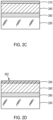
FIG. 2C illustrates a schematic cross-sectional view a device layer bonded to a transparent support wafer after removal of the growth wafer according to one or more embodiment of the disclosure; -
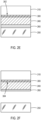
FIG. 2D illustrates a schematic cross-sectional view of a processed device layer bonded to a transparent support wafer according to one or more embodiment of the disclosure; -
FIG. 2E illustrates a schematic cross-sectional view of a processed device layer bonded to a second support wafer and a transparent support wafer according to one or more embodiment of the disclosure; -
FIG. 2F illustrates a schematic cross-sectional view of a processed device wafer with a second support wafer after separation from the transparent support wafer according to one or more embodiment; -
FIG. 2G illustrates a schematic cross-sectional view of a cleaned processed device wafer with a permanent support wafer and a separate transparent support wafer according to one or more embodiments of the disclosure; and -
FIG. 3 illustrates a schematic representation of a transparent support wafer with a plurality of device wafers arranged thereon. - To facilitate understanding, identical reference numerals have been used, where possible, to designate identical elements that are common to the figures. The figures are not drawn to scale. For example, the heights and widths of the various components are not drawn to scale.
- Before describing several exemplary embodiments of the disclosure, it is to be understood that the disclosure is not limited to the details of construction or process steps set forth in the following description. The disclosure is capable of other embodiments and of being practiced or being carried out in various ways.
- The term "substrate" as used herein according to one or more embodiments refers to a structure, intermediate or final, having a surface, or portion of a surface, upon which a process acts. In addition, reference to a substrate in some embodiments also refers to only a portion of the substrate, unless the context clearly indicates otherwise. Further, reference to depositing on a substrate according to some embodiments includes depositing on a bare substrate, or on a substrate with one or more films or features or materials deposited or formed thereon.
- In one or more embodiments, the "substrate" means any substrate or material surface formed on a substrate upon which film processing is performed during a fabrication process. In exemplary embodiments, a substrate surface on which processing is performed includes materials such as silicon, silicon oxide, silicon on insulator (SOI), strained silicon, amorphous silicon, doped silicon, carbon doped silicon oxides, germanium, gallium arsenide, glass, sapphire, and any other suitable materials such as metals, metal nitrides, III-nitrides (e.g., GaN, AlN, InN and alloys), metal alloys, and other conductive materials, depending on the application. Substrates include, without limitation, light emitting diode (LED) devices. Substrates in some embodiments are exposed to a pretreatment process to polish, etch, reduce, oxidize, hydroxylate, anneal, UV cure, e-beam cure and/or bake the substrate surface. In addition to film processing directly on the surface of the substrate itself, in some embodiments, any of the film processing steps disclosed are also performed on an underlayer formed on the substrate, and the term "substrate surface" is intended to include such underlayer as the context indicates. Thus, for example, where a film/layer or partial film/layer has been deposited onto a substrate surface, the exposed surface of the newly deposited film/layer becomes the substrate surface.
- The term "wafer" and "substrate" will be used interchangeably in the instant disclosure. Thus, as used herein, a wafer serves as the substrate for the formation of the LED devices described herein.
- In some embodiments, the basic drawbacks of organic bonds are overcome with a releasable inorganic bond. The high coefficient of thermal expansion (CTEs) of organic materials (>25ppm/°C) combined with the required bonding layer thickness (>10 µm), imparts excessive stress on thin film device layers during subsequent high temperature process steps. If the device wafer is particularly thin (<20 µm) it may buckle, warp and/or delaminate. However inorganic bonds are much thinner (<3 µm) and have a lower CTE (<25ppm/°C) and the resulting stress is much lower.
- Accordingly, with reference to
FIGS. 1 and2A through 2G ,methods 100 for manufacturing electronic devices (e.g., light emitting diodes (LEDs) are disclosed.FIG. 1 illustrates amethod 100 of manufacturing a light emitting diode (LED).FIGS. 2A through 2G show schematic cross-sectional representations of themethod 100 illustrated inFIG. 1 . While the disclosure refers to the device being formed as a light emitting diode, the skilled artisan will recognize that this is merely one possible electronic device and that other electronic or non-electronic devices can be formed by the disclosed processes. - In some embodiments, a
growth wafer 200 is bonded to asupport wafer 250. The bond is inorganic, e.g. oxide or metallic. In one or more embodiments, between the bond layer and thesupport wafer 250, there is arelease layer 260 that dissociates when exposed to laser radiation of appropriate intensity and wavelength. Thesupport wafer 250 is transparent to the laser radiation which is directed through the support wafer in a stitched pattern that completely covers the bond area. Thegrowth wafer 200 is thereby released from thesupport wafer 250. The release process is commonly known as Laser Lift-Off (LLO). Embodiments of the disclosure can be used where any wafer process flow requiring temporary mechanical support with subsequent process steps that are incompatible with organic bonding. - A
growth wafer 200 having afirst side 202 and asecond side 204 is illustrated inFIG. 2A . In some embodiments, thesecond side 204 of thegrowth wafer 200 has been processed previously to form adevice layer 210. In some embodiments, thesecond side 204 of thegrowth wafer 200 has not been processed prior tomethod 100 being performed. Thedevice layer 210 can be any suitable processed layer on thesecond side 204 of thegrowth wafer 200. In some embodiments, thedevice layer 210 is a semiconductor layer including, but not limited to, light emitting diodes (LEDs), transistors, capacitors, portions of light emitting diodes (e.g., active regions), portions of transistors (e.g., channels or doped source/drain regions), wirebond pads, bus bars, reflective layers, current carrying layers, contacts, intentionally roughened surfaces, etc. - At
operation 110, the backside (second side 204) of thegrowth wafer 200 is coated with an inorganic bonding layer 220 (e.g., a metal or oxide material) and prepared for bonding. Thedevice layer 210 forms thesecond side 204 of thegrowth wafer 200 at this point in the process so that forming theinorganic bonding layer 220 on thesecond side 204 of thegrowth wafer 200 results in theinorganic bonding layer 220 being formed on thedevice layer 210. Stated differently, theinorganic bonding layer 220 can be formed on thesecond side 214 of thedevice layer 210 while thefirst side 212 of thedevice layer 210 is formed on thesecond side 204 of thegrowth wafer 200. - The
inorganic bonding layer 220 of some embodiments is deposited onto thesecond side 204 of the growth wafer 200 (or thesecond side 214 of the device layer 210) using any suitable technique known to the skilled artisan, including, but not limited to, physical vapor deposition (PVD), chemical vapor deposition (CVD), atomic layer deposition (ALD), plasma-enhanced chemical vapor deposition (PECVD) or plasma-enhanced atomic layer deposition (PEALD), and spin-on techniques. In some embodiments, theinorganic bonding layer 220 comprises a metal layer and is deposited by physical vapor deposition. In some embodiments, theinorganic bonding layer 220 comprises an oxide and is deposited by ALD, PEALD, CVD or PECVD. - In some embodiments, the
growth wafer 200,device layer 210 andinorganic bonding layer 220 is prepared for bonding. In some embodiments, theinorganic bonding layer 220 is prepared for bonding by one or more of polishing thebonding surface 224 and/or protecting the first side 202 (also referred to as the front side) of thegrowth wafer 200 with a layer of photoresist (not shown). - A
transparent support wafer 250 having afirst side 252 and asecond side 254 is used for temporary support of thegrowth wafer 200 during processing. Thesupport wafer 250 is a transparent (relative to the laser wavelength required to release the bond formed in subsequent operations). TheLLO release layer 260 on thesupport wafer 250 is suitable for high intensity laser dissociation. This release layer is coated with a bonding layer (metal or oxide) matched to the device wafer and prepared for bonding. In some embodiments, preparing the device wafer includes polishing the bonding surface. - The
transparent support wafer 250 can be any suitable material that is transparent to the laser wavelength used for release operations. In some embodiments, thetransparent support wafer 250 comprises sapphire, silicon carbide, or glass. - At
operation 120, as shown inFIG. 2A , a laser lift-off (LLO)release layer 260 is deposited on thefirst side 252 of thetransparent support wafer 250. TheLLO release layer 260 has afirst side 262 and asecond side 264. In some embodiments, thefirst side 262 of theLLO release layer 260 is in direct contact with thefirst side 252 of thetransparent support wafer 250. As used in this manner, the term "direct contact" means that there is no intervening material between the stated components. - The
LLO release layer 260 of some embodiments comprises one or more of gallium nitride (GaN), aluminum indium gallium nitride having a general formula AlxInyGa1-x-yN, where 0<x+y≤1.0, or indium tin oxide (ITO) having the general formula InzSn1-zO, where 0≤z≤1.0. In some embodiments, theLLO release layer 260 comprises epitaxially grown gallium nitride (GaN). In some embodiments, theLLO release layer 260 comprises ITO deposited by one or more of sputtering or evaporation. - The
LLO release layer 260 can have any suitable thickness and be deposited by any suitable technique known to the skilled artisan. In some embodiments, theLLO release layer 260 has a thickness greater than or equal to 100 Å. In some embodiments, theLLO release layer 260 is deposited by one or more of epitaxy, sputtering, evaporation, plasma-enhanced chemical vapor deposition (PECVD) or metal organic vapor deposition (MOCVD). - At
operation 130, a matchinginorganic bonding layer 270 is formed on theLLO release layer 260. The matchinginorganic bonding layer 270 of some embodiments comprises the same material as theinorganic bonding layer 220 formed on thegrowth wafer 200. The matchinginorganic bonding layer 270 has afirst surface 272 and asecond side 274. In some embodiments, the matchinginorganic bonding layer 270 is formed on thefirst side 262 of theLLO release layer 260 so that thesecond side 274 of the matchinginorganic bonding layer 270 is in direct contact with thefirst side 262 of theLLO release layer 260. - In some embodiments, the matching
inorganic bonding layer 270 comprises a different material than theinorganic bonding layer 220. The matchinginorganic bonding layer 270 may comprise one or more metallic elements whileinorganic bonding layer 220 comprises different metallic elements, which upon heating in direct contact intermix to form a metallic alloy bond. The metal layers may be chosen such that the alloy formed has a higher melting point than one of the constituent elements, for example Au and In forming a Auln alloy. Numerous possible examples are readily found in the practice of soldering. In one or more embodiments of this sort, the matchinginorganic bonding layer 270 is a material that is compatible with theinorganic bonding layer 220 and may improve adhesion between theinorganic bonding layer 220 and the matchinginorganic bonding layer 270. In some embodiments, a very thin titanium (Ti) layer is formed betweeninorganic bonding layer 220 and the matchinginorganic bonding layer 270. As used in this manner, a "very thin" layer refers to a layer with a thickness less than or equal to 20 Å. - In some embodiments, the
inorganic bonding layer 220 and matchinginorganic bonding layer 270 comprise silicon oxide (SiOx). In some embodiments, the SiOx is replaced by other oxides which have superior HF resistance or other properties. - In some embodiments, the matching
inorganic bonding layer 270 comprises a silicon oxide layer formed directly on theLLO release layer 260 on thefirst side 252 of thetransparent support wafer 250. In some embodiments, each of theinorganic bonding layer 220 and the matchinginorganic bonding layer 270 independently have a final thickness in the range of 200Å to 400Å. In some embodiments, theinorganic bonding layer 220 and matchinginorganic bonding layer 270 are deposited and then polished. In some embodiments, the bonding layers are deposited with a thickness greater than 500Å and polishing brings the thickness down. - The
inorganic bonding layer 220 and matchinginorganic bonding layer 270 can be deposited by any suitable technique known to the skilled artisan. In some embodiments, each of theinorganic bonding layer 220 and matchinginorganic bonding layer 270 are deposited by physical vapor deposition (PVD), plasma-enhanced chemical vapor deposition (PECVD) or ebeam evaporation. - The order of the
operations - After the
growth wafer 200 andtransparent support wafer 250 have been prepared (i.e., the bonding layers have been prepared), atoperation 140, theinorganic bonding layer 220 on thegrowth wafer 200 is bonded with the matchinginorganic bonding layer 270 on thetransparent support wafer 250 to form aninorganic processing layer 240 between thetransparent support wafer 250 and thegrowth wafer 200, as shown inFIG. 2B . - The
inorganic bonding layer 220 can be bonded to the matchinginorganic bonding layer 270 by any suitable technique at any suitable temperature known to the skilled artisan. In some embodiments, bonding of theinorganic bonding layer 220 and the matchinginorganic bonding layer 270 occurs at room temperature. In some embodiments, bonding of theinorganic bonding layer 220 and the matchinginorganic bonding layer 270 occurs at a temperature up to and including 400 °C. Without being bound by any particular theory of operation, it is believed that increased temperature accelerates the bonding process and densifies and/or improves the bond strength. - The
method 100 up to this point results in the bonding of atransparent support wafer 250 to agrowth wafer 200, in which thetransparent support wafer 250 has a laser lift-off (LLO)release layer 260 formed on afirst side 252 of thetransparent support wafer 250 and aninorganic bonding layer 270 on theLLO release layer 260. Thegrowth wafer 200 has aninorganic bonding layer 220 on asecond side 204 of the growth wafer 200 (or thesecond side 214 of thedevice layer 210 formed on thesecond side 204 of the growth wafer 200). The bonding of thetransparent support wafer 250 to thegrowth wafer 200 comprises bonding theinorganic bonding layer 270 on thetransparent support wafer 250 with theinorganic bonding layer 220 on thegrowth wafer 200 to form aninorganic processing layer 240. - In some embodiments, the
inorganic bonding layer 220, the matchinginorganic bonding layer 270 and theinorganic processing layer 240 comprise silicon oxide (SiOx), and thetransparent support wafer 250 comprises sapphire. In some embodiments, a very thin titanium layer is formed on one or more of theinorganic bonding layer 220 or matchinginorganic bonding layer 270 prior to bonding so that there is a thin layer of titanium (not shown) within the thickness of theinorganic processing layer 240. - In some embodiments, the
inorganic processing layer 240 has a total thickness less than or equal to 5 µm. In some embodiments, theinorganic processing layer 240 has a total thickness less than or equal to 4 µm, 3 µm, 2 µm, 1.5 µm or 1 µm. In some embodiments, the total thickness of theinorganic processing layer 240 is 1.3 µm ± 0.5 µm. - At
operation 150, as shown inFIG. 2C , after thegrowth wafer 200 is bonded to thetransparent support wafer 250, thegrowth wafer 200 is removed. Removing thegrowth wafer 200 leaves thedevice layer 210 attached to theinorganic processing layer 240,LLO release layer 260 andtransparent support wafer 250. Removing thegrowth wafer 200 exposes thefirst side 212 of thedevice layer 210 for further processing, while protecting thesecond side 214 of thedevice layer 210. - The
growth wafer 200 can be separated from thedevice layer 210 by any suitable technique. For example, suitable techniques include but are not limited to grinding, chemical-mechanical polishing, laser lift-off (LLO), and/or wet etching to remove thegrowth wafer 200. - At
operation 160, as shown inFIG. 2D , one or more process steps are executed on thefirst side 212 of thedevice layer 210. Thesupport wafer 250 and any exposed bond material are chosen to be relatively unaffected by the process steps and not contaminate the processing tool or interfere with the processing. Processing of thedevice layer 210 is performed via thefirst side 212 of thedevice layer 210 to form a processeddevice layer 300. - In some embodiments,
optional operation 170 is performed to bond asecond support wafer 310 to thefirst side 302 of the processeddevice layer 300, as shown inFIG. 2E . After completion of the device layer processing, a second permanent or temporary support wafer can be attached to thefirst side 302 of the processeddevice layer 300. - At
operation 180, the processeddevice layer 300 is separated from thetransparent support wafer 250, as shown inFIG. 2F . In some embodiments, the separation process leaves theinorganic processing layer 240 on thesecond side 304 of the processeddevice layer 300. - In some embodiments, separating the processed
device layer 300 from thetransparent support wafer 250 comprises dissociating theLLO release layer 260 using laser pulses leaving theinorganic processing layer 240 on asecond side 304 of the processeddevice layer 300. - In some embodiments, a stitched pattern of high intensity pulses is used to release the device wafer (Laser Lift-Off). In some embodiments, the
LLO release layer 260 comprises gallium nitride (GaN) which dissociates into gallium (Ga) and molecular nitrogen (N2). In some embodiments, a 248nm Ar+ Excimer laser is used to expose the GaN layer to release the processeddevice layer 300 from thesupport wafer 250. - At
operation 180, the processeddevice layer 300 is cleaned to remove any residualLLO release layer 260 andinorganic processing layer 240, as shown inFIG. 2G . The result ofmethod 100 is a processeddevice layer 300 with an optional permanent or temporary support (second support wafer 310) and a separatetransparent support wafer 250. - In some embodiments, as illustrated in
FIG. 2F , an amount of theLLO release layer 260 remains on theinorganic processing layer 240.Optional operation 190 can be used to clean-up the residualLLO release layer 260 and/or perform additional processing steps on processeddevice layer 300. The residualLLO release layer 260 can be removed from theinorganic processing layer 240 in a separate process, or in the same process, as removal of theinorganic processing layer 240 from the processeddevice layer 300. - In some embodiments, the
transparent support wafer 250 is reusable after dissociating theLLO release layer 260. - In one or more embodiments, an adhesion promoting layer (not shown) is added between the inorganic bonding layers 220 and matching
bonding layer 270 and thegrowth wafer 200 and/ortransparent support wafers 250. The adhesion promoting layer can be any suitable material that increases the adhesion of the bonding layer material with the underlying layers. Suitable adhesion promoting layer include, but are not limited to, titanium (Ti) or silicon nitride. - Some embodiments of the disclosure are used with partial wafers. The partial wafers can be attached to a full-size carrier by oxide (or other suitable) bonding. Additionally, with the addition of support wafers on the frontside of the device wafer (post-processing) the process can be used to fabricate Thin Film Flip Chip or Chip Scale Packaged Devices where the growth substrates must be removed before device completion.
- For example,
FIG. 3 shows a schematic representation of a top-down view of atransparent support wafer 250 with a plurality ofgrowth wafers 200 arranged on thetransparent support wafer 250. The number ofgrowth wafers 200 illustrated is merely representative of one possible configuration and the skilled artisan will recognize that any suitable number of device wafers or portions of device wafers can be arranged on thetransparent support wafer 250 depending on, for example, the size of the device wafers and transparent support wafer. In some embodiments, there are more than onegrowth wafer 200 on a singletransparent support wafer 250. - In the illustrated embodiment, the
growth wafers 200 are shown on thefirst side 252 of thetransparent support wafer 250. After processing the device layers, theLLO release layer 260 is removed by illuminating through thetransparent support wafer 250. - Embodiment 1. A method (100) of manufacturing a light emitting diode (LED), the method comprising: bonding a transparent support wafer (250) to a growth wafer (200), the transparent support wafer (250) having a laser lift-off (LLO) release layer (260) formed on a first side (252) of the transparent support wafer (250) and an inorganic bonding layer (270) on the LLO release layer (260), the growth wafer (200) having a device layer (210) on a second side (204) of the growth wafer (200) and a matching inorganic bonding layer (220) on the device layer (210), wherein bonding the transparent support wafer (250) to the growth wafer (200) comprises bonding the inorganic bonding layer (270) on the transparent support wafer (250) with the matching inorganic bonding layer (220) on the growth wafer (200) to form an inorganic processing layer (240).
- Embodiment 2. The method of embodiment 1, further comprising removing the growth wafer (200), leaving the device layer (210) on the inorganic processing layer (240) on the LLO release layer (260) on the transparent support wafer (250).
- Embodiment 3. The method of embodiment 2, further comprising processing the device layer (210) via a first side (212) of the device layer (210) to form a processed device layer (300).
- Embodiment 4. The method of embodiment 3, further comprising attaching a second support wafer (310) to a second side (304) of the processed device layer (300).
- Embodiment 5. The method of embodiment 4, further comprising separating the processed device layer (300) from the transparent support wafer (250).
- Embodiment 6. The method of embodiment 5, wherein separating the processed device layer (300) from the transparent support wafer (250) comprises dissociating the LLO release layer (260) using laser pulses leaving the inorganic processing layer (240) on a second side (304) of the processed device layer (300).
- Embodiment 7. The method of embodiment 5 or 6, wherein the transparent support wafer (250) is reusable after dissociating the LLO release layer (260).
- Embodiment 8. The method of any of embodiments 5 to 7, further comprising removing the inorganic processing layer (240) from the second side (204) of the processed device layer (300).
- Embodiment 9. The method of any of embodiments 1 to 8, wherein the LLO release layer (260) comprises one or more of gallium nitride (GaN), aluminum indium gallium nitride having a general formula AlxlnyGa1-x-yN, where 0<x+y≤1.0, or indium tin oxide having the general formula InzSn1-zO, where 0≤z≤1.0.
- Embodiment 10. The method of any of embodiments 1 to 9, wherein the LLO release layer (260) has a thickness greater than or equal to 100 Å.
- Embodiment 11. The method of any of embodiments 1 to 10, wherein the transparent support wafer (250) comprises sapphire, silicon carbide, or glass.
- Embodiment 12. The method of any of embodiments 1 to 11, wherein a silicon oxide layer is formed directly on the LLO release layer (260) on the first side (252) of the transparent support wafer (250).
- Embodiment 13. The method of any of embodiments 1 to 12, wherein each of the inorganic bonding layer (220) and the matching inorganic bonding layer (270) are deposited by physical vapor deposition.
- Embodiment 14. The method of any of embodiments 1 to 13, wherein the LLO release layer (260) is deposited by metal organic vapor deposition (MOCVD).
- Embodiment 15. The method of any of embodiments 1 to 14, further comprising depositing the inorganic bonding layer (220) on the second side (204) of the growth wafer (200).
- Embodiment 16. The method of any of embodiments 1 to 15, further comprising depositing the LLO release layer (260) on the transparent support wafer (250) and the matching bonding layer (270) on the LLO release layer (260).
- Embodiment 17. The method of any of embodiments 1 to 16, wherein there are a plurality of growth wafers (200) bonded to one transparent support wafer (250).
- Embodiment 18. A method of manufacturing a light emitting diode (LED), the method comprising: depositing an inorganic bonding layer (220) on a device layer (210) on a second side (204) of a growth wafer (200); depositing a laser lift-off (LLO) release layer (260) on a first side (252) of a transparent support wafer (250), and a matching inorganic bonding layer (270) on the LLO release layer (260); bonding the inorganic bonding layer (220) on the growth wafer (200) with the matching inorganic bonding layer (270) on the transparent support wafer (250) to form an inorganic processing layer (240) between the transparent support wafer (250) and the growth wafer (200); removing the growth wafer (200) from the device layer (210), leaving the device layer (210) bonded to the inorganic processing layer (240); processing a first side (212) of the device layer (210) to form a processed device layer (300); attaching a second support wafer (310) to the first side (302) of the processed device layer (300); separating the processed device layer (300) from the transparent support wafer (250), leaving the inorganic processing layer (240) on a second side (304) of the processed device layer (300); and removing the inorganic processing layer (240) from the second side (304) of the device layer (210).
- Embodiment 19. The method of embodiment 18, wherein separating the processed growth wafer (200) from the transparent support wafer (250) comprises dissociating the LLO release layer (260) using laser pulses leaving the inorganic processing layer (240) on a second side (304) of the processed device layer (300).
- Embodiment 20. The method of embodiment 18 or 19, wherein the transparent support wafer (250) is reusable after dissociating the LLO release layer (260).
- Embodiment 21. The method of any of embodiments 18 to 20, wherein the LLO release layer (260) comprises one or more of gallium nitride (GaN), aluminum indium gallium nitride having a general formula AlxlnyGa1-x-yN, where 0<x+y≤1.0, or indium tin oxide having the general formula InzSn1-zO, where 0≤z≤1.0.
- Embodiment 22. The method of any of embodiments 18 to 21, wherein the LLO release layer (260) has a thickness greater than or equal to 100 Å.
- Embodiment 23. The method of any of embodiments 18 to 22, wherein the transparent support wafer (250) comprises sapphire, silicon carbide or glass.
- Embodiment 24. The method of any of embodiments 18 to 23, wherein a silicon oxide layer is formed directly on the LLO release layer (260) on the first side (252) of the transparent support wafer (250).
- Embodiment 25. The method of any of embodiments 18 to 23, wherein each of the inorganic bonding layer (220) and the matching inorganic bonding layer (270) are deposited by physical vapor deposition.
- The use of the terms "a" and "an" and "the" and similar referents in the context of describing the materials and methods discussed herein (especially in the context of the following claims) are to be construed to cover both the singular and the plural, unless otherwise indicated herein or clearly contradicted by context. Recitation of ranges of values herein are merely intended to serve as a shorthand method of referring individually to each separate value falling within the range, unless otherwise indicated herein, and each separate value is incorporated into the specification as if it were individually recited herein. All methods described herein can be performed in any suitable order unless otherwise indicated herein or otherwise clearly contradicted by context. The use of any and all examples, or exemplary language (e.g., "such as") provided herein, is intended merely to better illuminate the materials and methods and does not pose a limitation on the scope unless otherwise claimed. No language in the specification should be construed as indicating any non-claimed element as essential to the practice of the disclosed materials and methods.
- Reference throughout this specification to "one embodiment," "certain embodiments," "one or more embodiments" or "an embodiment" means that a particular feature, structure, material, or characteristic described in connection with the embodiment is included in at least one embodiment of the disclosure. Thus, the appearances of the phrases such as "in one or more embodiments," "in certain embodiments," "in one embodiment" or "in an embodiment" in various places throughout this specification are not necessarily referring to the same embodiment of the disclosure. In one or more embodiments, the particular features, structures, materials, or characteristics are combined in any suitable manner.
- Although the disclosure herein has been described with reference to particular embodiments, it is to be understood that these embodiments are merely illustrative of the principles and applications of the present disclosure. It will be apparent to those skilled in the art that various modifications and variations can be made to the method and apparatus of the present disclosure without departing from the spirit and scope of the disclosure. Thus, it is intended that the present disclosure include modifications and variations that are within the scope of the appended claims and their equivalents.
- Furthermore, the following further exemplary embodiments of the invention are disclosed:
- Embodiment 1: A method of manufacturing a light emitting diode (LED), the method comprising:
bonding a transparent support wafer to a growth wafer, the transparent support wafer having a laser lift-off (LLO) release layer formed on a first side of the transparent support wafer and an inorganic bonding layer on the LLO release layer, the growth wafer having a device layer on a second side of the growth wafer and a matching inorganic bonding layer on the device layer, wherein bonding the transparent support wafer to the growth wafer comprises bonding the inorganic bonding layer on the transparent support wafer with the matching inorganic bonding layer on the growth wafer to form an inorganic processing layer. - Embodiment 2: The method of embodiment 1, further comprising removing the growth wafer, leaving the device layer on the inorganic processing layer on the LLO release layer on the transparent support wafer.
- Embodiment 3: The method of embodiment 2, further comprising processing the device layer via a first side of the device layer to form a processed device layer.
- Embodiment 4: The method of embodiment 3, further comprising attaching a second support wafer to a second side of the processed device layer.
- Embodiment 5: The method of embodiment 4, further comprising separating the processed device layer from the transparent support wafer.
- Embodiment 6: The method of embodiment 5, wherein separating the processed device layer from the transparent support wafer comprises dissociating the LLO release layer using laser pulses leaving the inorganic processing layer on a second side of the processed device layer.
- Embodiment 7: The method of embodiment 5, wherein the transparent support wafer is reusable after dissociating the LLO release layer.
- Embodiment 8: The method of embodiment 5, further comprising removing the inorganic processing layer from the second side of the processed device layer.
- Embodiment 9: The method of embodiment 1, wherein the LLO release layer comprises one or more of gallium nitride (GaN), aluminum indium gallium nitride having a general formula AlxInyGa1-x-yN, where 0<x+y≤1.0, or indium tin oxide having the general formula InzSn1-zO, where 0≤z≤1.0.
- Embodiment 10: The method of embodiment 1, wherein the LLO release layer has a thickness greater than or equal to 100 Å.
- Embodiment 11: The method of embodiment 1, wherein the transparent support wafer comprises sapphire, silicon carbide, or glass.
- Embodiment 12: The method of embodiment 1, wherein a silicon oxide layer is formed directly on the LLO release layer on the first side of the transparent support wafer.
- Embodiment 13: The method of embodiment 1, further comprising depositing the inorganic bonding layer on the second side of the growth wafer.
- Embodiment 14: The method of embodiment 1, further comprising depositing the LLO release layer on the transparent support wafer and the matching bonding layer on the LLO release layer.
- Embodiment 15: The method of embodiment 1, wherein there are a plurality of growth wafers bonded to one transparent support wafer.
- Embodiment 16: A method of manufacturing a light emitting diode (LED), the method comprising:
- depositing an inorganic bonding layer on a device layer on a second side of a growth wafer;
- depositing a laser lift-off (LLO) release layer on a first side of a transparent support wafer, and a matching inorganic bonding layer on the LLO release layer;
- bonding the inorganic bonding layer on the growth wafer with the matching inorganic bonding layer on the transparent support wafer to form an inorganic processing layer between the transparent support wafer and the growth wafer;
- removing the growth wafer from the device layer, leaving the device layer bonded to the inorganic processing layer;
- processing a first side of the device layer to form a processed device layer;
- attaching a second support wafer to the first side of the processed device layer;
- separating the processed device layer from the transparent support wafer, leaving the inorganic processing layer on a second side of the processed device layer; and
- removing the inorganic processing layer from the second side of the device layer.
- Embodiment 17: The method of embodiment 16, wherein separating the processed growth wafer from the transparent support wafer comprises dissociating the LLO release layer using laser pulses leaving the inorganic processing layer on a second side of the processed device layer.
- Embodiment 18: The method of embodiment 17, wherein the transparent support wafer is reusable after dissociating the LLO release layer.
- Embodiment 19: The method of embodiment 16, wherein the LLO release layer comprises one or more of gallium nitride (GaN), aluminum indium gallium nitride having a general formula AlxInyGa1-x-yN, where 0<x+y≤1.0, or indium tin oxide having the general formula InzSn1-zO, where 0≤z≤1.0.
- Embodiment 20: The method of embodiment 16, wherein the transparent support wafer comprises sapphire, silicon carbide or glass.
Claims (15)
- A method of manufacturing a light emitting diode (LED), the method comprising:
bonding a transparent support wafer to a growth wafer, the transparent support wafer having a laser lift-off (LLO) release layer formed on a first side of the transparent support wafer and an inorganic bonding layer on the LLO release layer, the growth wafer having a device layer on a second side of the growth wafer and a matching inorganic bonding layer on the device layer, wherein bonding the transparent support wafer to the growth wafer comprises bonding the inorganic bonding layer on the transparent support wafer with the matching inorganic bonding layer on the growth wafer to form an inorganic processing layer. - The method of claim 1, further comprising removing the growth wafer, leaving the device layer on the inorganic processing layer on the LLO release layer on the transparent support wafer.
- The method of claim 2, further comprising processing the device layer via a first side of the device layer to form a processed device layer.
- The method of claim 3, further comprising attaching a second support wafer to a second side of the processed device layer.
- The method of claim 4, further comprising separating the processed device layer from the transparent support wafer.
- The method of claim 5, further comprising removing the inorganic processing layer from the second side of the processed device layer.
- The method of claim 1, wherein the LLO release layer has a thickness greater than or equal to 100 Å.
- The method of claim 1, wherein a silicon oxide layer is formed directly on the LLO release layer on the first side of the transparent support wafer.
- The method of claim 1, further comprising depositing the inorganic bonding layer on the second side of the growth wafer.
- The method of claim 1, further comprising depositing the LLO release layer on the transparent support wafer and the matching bonding layer on the LLO release layer.
- A method of manufacturing a light emitting diode (LED), the method comprising:depositing an inorganic bonding layer on a device layer on a second side of a growth wafer;depositing a laser lift-off (LLO) release layer on a first side of a transparent support wafer, and a matching inorganic bonding layer on the LLO release layer;bonding the inorganic bonding layer on the growth wafer with the matching inorganic bonding layer on the transparent support wafer to form an inorganic processing layer between the transparent support wafer and the growth wafer;removing the growth wafer from the device layer, leaving the device layer bonded to the inorganic processing layer;processing a first side of the device layer to form a processed device layer;attaching a second support wafer to the first side of the processed device layer;separating the processed device layer from the transparent support wafer, leaving the inorganic processing layer on a second side of the processed device layer; andremoving the inorganic processing layer from the second side of the device layer.
- The method of claim 11 or of claim 5, wherein separating the processed growth wafer or the processed device layer from the transparent support wafer comprises dissociating the LLO release layer using laser pulses leaving the inorganic processing layer on a second side of the processed device layer.
- The method of claim 12 or of claim 5, wherein the transparent support wafer is reusable after dissociating the LLO release layer.
- The method of claim 11 or of claim 1, wherein the LLO release layer comprises one or more of gallium nitride (GaN), aluminum indium gallium nitride having a general formula AlxInyGa1-x-yN, where 0<x+y≤1.0, or indium tin oxide having the general formula InzSn1-zO, where 0≤z≤1.0.
- The method of claim 11 or of claim 1, wherein the transparent support wafer comprises sapphire, silicon carbide or glass.
Applications Claiming Priority (1)
| Application Number | Priority Date | Filing Date | Title |
|---|---|---|---|
| US18/110,699 US20240282884A1 (en) | 2023-02-16 | 2023-02-16 | Led device formation using releasable inorganic wafer bond |
Publications (1)
| Publication Number | Publication Date |
|---|---|
| EP4418334A1 true EP4418334A1 (en) | 2024-08-21 |
Family
ID=89977251
Family Applications (1)
| Application Number | Title | Priority Date | Filing Date |
|---|---|---|---|
| EP24157873.1A Pending EP4418334A1 (en) | 2023-02-16 | 2024-02-15 | Led device formation using releasable inorganic wafer bond |
Country Status (3)
| Country | Link |
|---|---|
| US (1) | US20240282884A1 (en) |
| EP (1) | EP4418334A1 (en) |
| CN (1) | CN118507601A (en) |
Citations (4)
| Publication number | Priority date | Publication date | Assignee | Title |
|---|---|---|---|---|
| US20060270075A1 (en) * | 2005-05-27 | 2006-11-30 | Leem See J | Method of manufacturing light emitting diodes |
| WO2010015878A2 (en) * | 2008-08-06 | 2010-02-11 | S.O.I. Tec Silicon On Insulator Technologies | Process for modifying a substrate |
| US20110062467A1 (en) * | 2008-03-24 | 2011-03-17 | Lg Innotek Co., Ltd. | Light emitting device and manufacturing method thereof |
| CN102106006A (en) * | 2008-06-02 | 2011-06-22 | 高丽大学校 | Support substrate for manufacturing semiconductor light emitting device and semiconductor light emitting device using support substrate |
-
2023
- 2023-02-16 US US18/110,699 patent/US20240282884A1/en active Pending
-
2024
- 2024-02-05 CN CN202410164125.1A patent/CN118507601A/en active Pending
- 2024-02-15 EP EP24157873.1A patent/EP4418334A1/en active Pending
Patent Citations (4)
| Publication number | Priority date | Publication date | Assignee | Title |
|---|---|---|---|---|
| US20060270075A1 (en) * | 2005-05-27 | 2006-11-30 | Leem See J | Method of manufacturing light emitting diodes |
| US20110062467A1 (en) * | 2008-03-24 | 2011-03-17 | Lg Innotek Co., Ltd. | Light emitting device and manufacturing method thereof |
| CN102106006A (en) * | 2008-06-02 | 2011-06-22 | 高丽大学校 | Support substrate for manufacturing semiconductor light emitting device and semiconductor light emitting device using support substrate |
| WO2010015878A2 (en) * | 2008-08-06 | 2010-02-11 | S.O.I. Tec Silicon On Insulator Technologies | Process for modifying a substrate |
Also Published As
| Publication number | Publication date |
|---|---|
| US20240282884A1 (en) | 2024-08-22 |
| CN118507601A (en) | 2024-08-16 |
Similar Documents
| Publication | Publication Date | Title |
|---|---|---|
| CN100377368C (en) | Manufacturing method of GaN-based semiconductor element | |
| JP5393158B2 (en) | Nitride semiconductor device and manufacturing method thereof | |
| EP2600389B1 (en) | Method for bonding semiconductor substrates | |
| US10510577B2 (en) | Lift off process for chip scale package solid state devices on engineered substrate | |
| KR100797208B1 (en) | In particular, the manufacturing process of the detachable semiconductor assembly forming substrates for electronics, optoelectronics and optics | |
| JP2009527913A5 (en) | ||
| JP7190245B2 (en) | vertical gallium nitride schottky diode | |
| TWI754710B (en) | Method and system for vertical power devices | |
| US20110147704A1 (en) | Semiconductor light-emitting device with passivation layer | |
| KR20140048268A (en) | Method of bonding a semiconductor device to a support substrate | |
| US20110140081A1 (en) | Method for fabricating semiconductor light-emitting device with double-sided passivation | |
| JP2007529099A (en) | Production of conductive metal layers on semiconductor devices. | |
| WO2005029573A1 (en) | Fabrication of semiconductor devices | |
| WO2016149629A1 (en) | Strain relief epitaxial lift-off via pre-patterned mesas | |
| KR20120118032A (en) | Semiconductor light emitting device with layer compensating for the thermal expansion of the substrate | |
| US8309377B2 (en) | Fabrication of reflective layer on semiconductor light emitting devices | |
| CN113707770A (en) | Processing technology of silicon substrate GaN | |
| US20240282884A1 (en) | Led device formation using releasable inorganic wafer bond | |
| US20140084422A1 (en) | Reclaimed Wafer And A Method For Reclaiming A Wafer | |
| JP7056826B2 (en) | Manufacturing method of semiconductor device | |
| WO2024039870A1 (en) | Suction cup device and method for removing sapphire substrate | |
| CN106783726A (en) | Compound substrate and preparation method thereof, semiconductor devices |
Legal Events
| Date | Code | Title | Description |
|---|---|---|---|
| PUAI | Public reference made under article 153(3) epc to a published international application that has entered the european phase |
Free format text: ORIGINAL CODE: 0009012 |
|
| STAA | Information on the status of an ep patent application or granted ep patent |
Free format text: STATUS: REQUEST FOR EXAMINATION WAS MADE |
|
| 17P | Request for examination filed |
Effective date: 20240215 |
|
| AK | Designated contracting states |
Kind code of ref document: A1 Designated state(s): AL AT BE BG CH CY CZ DE DK EE ES FI FR GB GR HR HU IE IS IT LI LT LU LV MC ME MK MT NL NO PL PT RO RS SE SI SK SM TR |