EP4418289A2 - Core-shell particles for dielectric of a multilayered ceramic capacitor (mlcc) and manufacturing method thereof - Google Patents
Core-shell particles for dielectric of a multilayered ceramic capacitor (mlcc) and manufacturing method thereof Download PDFInfo
- Publication number
- EP4418289A2 EP4418289A2 EP23186979.3A EP23186979A EP4418289A2 EP 4418289 A2 EP4418289 A2 EP 4418289A2 EP 23186979 A EP23186979 A EP 23186979A EP 4418289 A2 EP4418289 A2 EP 4418289A2
- Authority
- EP
- European Patent Office
- Prior art keywords
- mole
- dielectric
- core
- parts
- shell structure
- Prior art date
- Legal status (The legal status is an assumption and is not a legal conclusion. Google has not performed a legal analysis and makes no representation as to the accuracy of the status listed.)
- Pending
Links
- 239000011258 core-shell material Substances 0.000 title claims abstract description 56
- 238000004519 manufacturing process Methods 0.000 title claims abstract description 18
- 239000003985 ceramic capacitor Substances 0.000 title description 3
- 239000002245 particle Substances 0.000 title description 3
- 239000003990 capacitor Substances 0.000 claims abstract description 108
- 239000000654 additive Substances 0.000 claims description 60
- 230000000996 additive effect Effects 0.000 claims description 58
- 150000004706 metal oxides Chemical class 0.000 claims description 58
- 229910052788 barium Inorganic materials 0.000 claims description 38
- 229910001338 liquidmetal Inorganic materials 0.000 claims description 37
- 239000000843 powder Substances 0.000 claims description 37
- 229910052719 titanium Inorganic materials 0.000 claims description 33
- 229910052718 tin Inorganic materials 0.000 claims description 30
- 239000000919 ceramic Substances 0.000 claims description 29
- 238000000034 method Methods 0.000 claims description 26
- 229910044991 metal oxide Inorganic materials 0.000 claims description 21
- 238000010304 firing Methods 0.000 claims description 20
- 239000011777 magnesium Substances 0.000 claims description 18
- 239000011572 manganese Substances 0.000 claims description 18
- 229910052791 calcium Inorganic materials 0.000 claims description 16
- 239000011651 chromium Substances 0.000 claims description 16
- 239000002904 solvent Substances 0.000 claims description 16
- 229910052712 strontium Inorganic materials 0.000 claims description 16
- ATJFFYVFTNAWJD-UHFFFAOYSA-N Tin Chemical compound [Sn] ATJFFYVFTNAWJD-UHFFFAOYSA-N 0.000 claims description 15
- 229910052726 zirconium Inorganic materials 0.000 claims description 15
- VYPSYNLAJGMNEJ-UHFFFAOYSA-N Silicium dioxide Chemical compound O=[Si]=O VYPSYNLAJGMNEJ-UHFFFAOYSA-N 0.000 claims description 13
- 229910010252 TiO3 Inorganic materials 0.000 claims description 13
- VTYYLEPIZMXCLO-UHFFFAOYSA-L Calcium carbonate Chemical compound [Ca+2].[O-]C([O-])=O VTYYLEPIZMXCLO-UHFFFAOYSA-L 0.000 claims description 12
- AYJRCSIUFZENHW-UHFFFAOYSA-L barium carbonate Chemical compound [Ba+2].[O-]C([O-])=O AYJRCSIUFZENHW-UHFFFAOYSA-L 0.000 claims description 12
- NUJOXMJBOLGQSY-UHFFFAOYSA-N manganese dioxide Chemical compound O=[Mn]=O NUJOXMJBOLGQSY-UHFFFAOYSA-N 0.000 claims description 12
- 229910002113 barium titanate Inorganic materials 0.000 claims description 10
- FYYHWMGAXLPEAU-UHFFFAOYSA-N Magnesium Chemical compound [Mg] FYYHWMGAXLPEAU-UHFFFAOYSA-N 0.000 claims description 9
- PWHULOQIROXLJO-UHFFFAOYSA-N Manganese Chemical compound [Mn] PWHULOQIROXLJO-UHFFFAOYSA-N 0.000 claims description 9
- 229910052749 magnesium Inorganic materials 0.000 claims description 9
- 229910052748 manganese Inorganic materials 0.000 claims description 9
- VYZAMTAEIAYCRO-UHFFFAOYSA-N Chromium Chemical compound [Cr] VYZAMTAEIAYCRO-UHFFFAOYSA-N 0.000 claims description 8
- GYHNNYVSQQEPJS-UHFFFAOYSA-N Gallium Chemical compound [Ga] GYHNNYVSQQEPJS-UHFFFAOYSA-N 0.000 claims description 8
- XUIMIQQOPSSXEZ-UHFFFAOYSA-N Silicon Chemical compound [Si] XUIMIQQOPSSXEZ-UHFFFAOYSA-N 0.000 claims description 8
- 230000002378 acidificating effect Effects 0.000 claims description 8
- 229910052782 aluminium Inorganic materials 0.000 claims description 8
- XAGFODPZIPBFFR-UHFFFAOYSA-N aluminium Chemical compound [Al] XAGFODPZIPBFFR-UHFFFAOYSA-N 0.000 claims description 8
- 229910052787 antimony Inorganic materials 0.000 claims description 8
- WATWJIUSRGPENY-UHFFFAOYSA-N antimony atom Chemical compound [Sb] WATWJIUSRGPENY-UHFFFAOYSA-N 0.000 claims description 8
- DSAJWYNOEDNPEQ-UHFFFAOYSA-N barium atom Chemical compound [Ba] DSAJWYNOEDNPEQ-UHFFFAOYSA-N 0.000 claims description 8
- 229910052804 chromium Inorganic materials 0.000 claims description 8
- 229910052733 gallium Inorganic materials 0.000 claims description 8
- 229910052732 germanium Inorganic materials 0.000 claims description 8
- GNPVGFCGXDBREM-UHFFFAOYSA-N germanium atom Chemical compound [Ge] GNPVGFCGXDBREM-UHFFFAOYSA-N 0.000 claims description 8
- 229910052735 hafnium Inorganic materials 0.000 claims description 8
- VBJZVLUMGGDVMO-UHFFFAOYSA-N hafnium atom Chemical compound [Hf] VBJZVLUMGGDVMO-UHFFFAOYSA-N 0.000 claims description 8
- 229910052738 indium Inorganic materials 0.000 claims description 8
- APFVFJFRJDLVQX-UHFFFAOYSA-N indium atom Chemical compound [In] APFVFJFRJDLVQX-UHFFFAOYSA-N 0.000 claims description 8
- 238000002156 mixing Methods 0.000 claims description 8
- 229910052710 silicon Inorganic materials 0.000 claims description 8
- 239000010703 silicon Substances 0.000 claims description 8
- LEONUFNNVUYDNQ-UHFFFAOYSA-N vanadium atom Chemical compound [V] LEONUFNNVUYDNQ-UHFFFAOYSA-N 0.000 claims description 8
- 229910052684 Cerium Inorganic materials 0.000 claims description 7
- 229910052692 Dysprosium Inorganic materials 0.000 claims description 7
- 229910052691 Erbium Inorganic materials 0.000 claims description 7
- 229910052693 Europium Inorganic materials 0.000 claims description 7
- 229910052688 Gadolinium Inorganic materials 0.000 claims description 7
- 229910052689 Holmium Inorganic materials 0.000 claims description 7
- 229910052765 Lutetium Inorganic materials 0.000 claims description 7
- 229910052779 Neodymium Inorganic materials 0.000 claims description 7
- 229910052777 Praseodymium Inorganic materials 0.000 claims description 7
- 229910052773 Promethium Inorganic materials 0.000 claims description 7
- 229910052772 Samarium Inorganic materials 0.000 claims description 7
- 229910052771 Terbium Inorganic materials 0.000 claims description 7
- 229910052775 Thulium Inorganic materials 0.000 claims description 7
- 229910009650 Ti1-yZry Inorganic materials 0.000 claims description 7
- 229910052769 Ytterbium Inorganic materials 0.000 claims description 7
- 229910052768 actinide Inorganic materials 0.000 claims description 7
- 150000001255 actinides Chemical class 0.000 claims description 7
- GWXLDORMOJMVQZ-UHFFFAOYSA-N cerium Chemical compound [Ce] GWXLDORMOJMVQZ-UHFFFAOYSA-N 0.000 claims description 7
- KBQHZAAAGSGFKK-UHFFFAOYSA-N dysprosium atom Chemical compound [Dy] KBQHZAAAGSGFKK-UHFFFAOYSA-N 0.000 claims description 7
- UYAHIZSMUZPPFV-UHFFFAOYSA-N erbium Chemical compound [Er] UYAHIZSMUZPPFV-UHFFFAOYSA-N 0.000 claims description 7
- OGPBJKLSAFTDLK-UHFFFAOYSA-N europium atom Chemical compound [Eu] OGPBJKLSAFTDLK-UHFFFAOYSA-N 0.000 claims description 7
- UIWYJDYFSGRHKR-UHFFFAOYSA-N gadolinium atom Chemical compound [Gd] UIWYJDYFSGRHKR-UHFFFAOYSA-N 0.000 claims description 7
- KJZYNXUDTRRSPN-UHFFFAOYSA-N holmium atom Chemical compound [Ho] KJZYNXUDTRRSPN-UHFFFAOYSA-N 0.000 claims description 7
- 229910052746 lanthanum Inorganic materials 0.000 claims description 7
- FZLIPJUXYLNCLC-UHFFFAOYSA-N lanthanum atom Chemical compound [La] FZLIPJUXYLNCLC-UHFFFAOYSA-N 0.000 claims description 7
- OHSVLFRHMCKCQY-UHFFFAOYSA-N lutetium atom Chemical compound [Lu] OHSVLFRHMCKCQY-UHFFFAOYSA-N 0.000 claims description 7
- QEFYFXOXNSNQGX-UHFFFAOYSA-N neodymium atom Chemical compound [Nd] QEFYFXOXNSNQGX-UHFFFAOYSA-N 0.000 claims description 7
- PUDIUYLPXJFUGB-UHFFFAOYSA-N praseodymium atom Chemical compound [Pr] PUDIUYLPXJFUGB-UHFFFAOYSA-N 0.000 claims description 7
- VQMWBBYLQSCNPO-UHFFFAOYSA-N promethium atom Chemical compound [Pm] VQMWBBYLQSCNPO-UHFFFAOYSA-N 0.000 claims description 7
- KZUNJOHGWZRPMI-UHFFFAOYSA-N samarium atom Chemical compound [Sm] KZUNJOHGWZRPMI-UHFFFAOYSA-N 0.000 claims description 7
- GZCRRIHWUXGPOV-UHFFFAOYSA-N terbium atom Chemical compound [Tb] GZCRRIHWUXGPOV-UHFFFAOYSA-N 0.000 claims description 7
- FRNOGLGSGLTDKL-UHFFFAOYSA-N thulium atom Chemical compound [Tm] FRNOGLGSGLTDKL-UHFFFAOYSA-N 0.000 claims description 7
- 229910052861 titanite Inorganic materials 0.000 claims description 7
- NAWDYIZEMPQZHO-UHFFFAOYSA-N ytterbium Chemical compound [Yb] NAWDYIZEMPQZHO-UHFFFAOYSA-N 0.000 claims description 7
- 229910052727 yttrium Inorganic materials 0.000 claims description 7
- VWQVUPCCIRVNHF-UHFFFAOYSA-N yttrium atom Chemical compound [Y] VWQVUPCCIRVNHF-UHFFFAOYSA-N 0.000 claims description 7
- PNEYBMLMFCGWSK-UHFFFAOYSA-N aluminium oxide Inorganic materials [O-2].[O-2].[O-2].[Al+3].[Al+3] PNEYBMLMFCGWSK-UHFFFAOYSA-N 0.000 claims description 6
- 229910000019 calcium carbonate Inorganic materials 0.000 claims description 6
- 229910052681 coesite Inorganic materials 0.000 claims description 6
- 150000001875 compounds Chemical class 0.000 claims description 6
- 229910052593 corundum Inorganic materials 0.000 claims description 6
- 229910052906 cristobalite Inorganic materials 0.000 claims description 6
- NLQFUUYNQFMIJW-UHFFFAOYSA-N dysprosium(III) oxide Inorganic materials O=[Dy]O[Dy]=O NLQFUUYNQFMIJW-UHFFFAOYSA-N 0.000 claims description 6
- 239000002563 ionic surfactant Substances 0.000 claims description 6
- 239000000377 silicon dioxide Substances 0.000 claims description 6
- 229910052682 stishovite Inorganic materials 0.000 claims description 6
- 229910052905 tridymite Inorganic materials 0.000 claims description 6
- 229910001845 yogo sapphire Inorganic materials 0.000 claims description 6
- JRPBQTZRNDNNOP-UHFFFAOYSA-N barium titanate Chemical compound [Ba+2].[Ba+2].[O-][Ti]([O-])([O-])[O-] JRPBQTZRNDNNOP-UHFFFAOYSA-N 0.000 claims description 5
- 235000010216 calcium carbonate Nutrition 0.000 claims description 2
- 235000012239 silicon dioxide Nutrition 0.000 claims description 2
- 229910052751 metal Inorganic materials 0.000 description 42
- 239000002184 metal Substances 0.000 description 42
- 239000010936 titanium Substances 0.000 description 36
- PXHVJJICTQNCMI-UHFFFAOYSA-N nickel Substances [Ni] PXHVJJICTQNCMI-UHFFFAOYSA-N 0.000 description 31
- 239000011347 resin Substances 0.000 description 26
- 229920005989 resin Polymers 0.000 description 26
- 238000007747 plating Methods 0.000 description 18
- 239000011575 calcium Substances 0.000 description 16
- 239000000203 mixture Substances 0.000 description 15
- 239000010949 copper Substances 0.000 description 14
- 239000011230 binding agent Substances 0.000 description 12
- 230000000052 comparative effect Effects 0.000 description 12
- 239000000470 constituent Substances 0.000 description 11
- 229910052759 nickel Inorganic materials 0.000 description 11
- 229910052802 copper Inorganic materials 0.000 description 9
- RYGMFSIKBFXOCR-UHFFFAOYSA-N Copper Chemical compound [Cu] RYGMFSIKBFXOCR-UHFFFAOYSA-N 0.000 description 8
- 238000000137 annealing Methods 0.000 description 8
- 229910045601 alloy Inorganic materials 0.000 description 7
- 239000000956 alloy Substances 0.000 description 7
- 239000012298 atmosphere Substances 0.000 description 7
- 239000000463 material Substances 0.000 description 7
- KDLHZDBZIXYQEI-UHFFFAOYSA-N palladium Substances [Pd] KDLHZDBZIXYQEI-UHFFFAOYSA-N 0.000 description 7
- ZWEHNKRNPOVVGH-UHFFFAOYSA-N 2-Butanone Chemical compound CCC(C)=O ZWEHNKRNPOVVGH-UHFFFAOYSA-N 0.000 description 6
- CSCPPACGZOOCGX-UHFFFAOYSA-N Acetone Chemical compound CC(C)=O CSCPPACGZOOCGX-UHFFFAOYSA-N 0.000 description 6
- YXFVVABEGXRONW-UHFFFAOYSA-N Toluene Chemical compound CC1=CC=CC=C1 YXFVVABEGXRONW-UHFFFAOYSA-N 0.000 description 6
- 239000011521 glass Substances 0.000 description 6
- BASFCYQUMIYNBI-UHFFFAOYSA-N platinum Chemical compound [Pt] BASFCYQUMIYNBI-UHFFFAOYSA-N 0.000 description 6
- 239000003989 dielectric material Substances 0.000 description 5
- 230000000694 effects Effects 0.000 description 5
- 239000010931 gold Substances 0.000 description 5
- 239000004014 plasticizer Substances 0.000 description 5
- 238000000576 coating method Methods 0.000 description 4
- 230000007423 decrease Effects 0.000 description 4
- 239000002270 dispersing agent Substances 0.000 description 4
- 238000005498 polishing Methods 0.000 description 4
- 229910052761 rare earth metal Inorganic materials 0.000 description 4
- 238000007650 screen-printing Methods 0.000 description 4
- XLYOFNOQVPJJNP-UHFFFAOYSA-N water Substances O XLYOFNOQVPJJNP-UHFFFAOYSA-N 0.000 description 4
- IJGRMHOSHXDMSA-UHFFFAOYSA-N Atomic nitrogen Chemical compound N#N IJGRMHOSHXDMSA-UHFFFAOYSA-N 0.000 description 3
- MUBZPKHOEPUJKR-UHFFFAOYSA-N Oxalic acid Chemical compound OC(=O)C(O)=O MUBZPKHOEPUJKR-UHFFFAOYSA-N 0.000 description 3
- RTAQQCXQSZGOHL-UHFFFAOYSA-N Titanium Chemical compound [Ti] RTAQQCXQSZGOHL-UHFFFAOYSA-N 0.000 description 3
- QVGXLLKOCUKJST-UHFFFAOYSA-N atomic oxygen Chemical compound [O] QVGXLLKOCUKJST-UHFFFAOYSA-N 0.000 description 3
- 230000005540 biological transmission Effects 0.000 description 3
- 239000011248 coating agent Substances 0.000 description 3
- 230000007547 defect Effects 0.000 description 3
- 229910001873 dinitrogen Inorganic materials 0.000 description 3
- 239000007788 liquid Substances 0.000 description 3
- 239000001301 oxygen Substances 0.000 description 3
- 229910052760 oxygen Inorganic materials 0.000 description 3
- 229910052763 palladium Inorganic materials 0.000 description 3
- 238000007639 printing Methods 0.000 description 3
- 239000002994 raw material Substances 0.000 description 3
- 150000003839 salts Chemical class 0.000 description 3
- 238000001878 scanning electron micrograph Methods 0.000 description 3
- 229910052709 silver Inorganic materials 0.000 description 3
- OAYXUHPQHDHDDZ-UHFFFAOYSA-N 2-(2-butoxyethoxy)ethanol Chemical compound CCCCOCCOCCO OAYXUHPQHDHDDZ-UHFFFAOYSA-N 0.000 description 2
- ZTQSAGDEMFDKMZ-UHFFFAOYSA-N Butyraldehyde Chemical compound CCCC=O ZTQSAGDEMFDKMZ-UHFFFAOYSA-N 0.000 description 2
- LFQSCWFLJHTTHZ-UHFFFAOYSA-N Ethanol Chemical compound CCO LFQSCWFLJHTTHZ-UHFFFAOYSA-N 0.000 description 2
- 239000001856 Ethyl cellulose Substances 0.000 description 2
- ZZSNKZQZMQGXPY-UHFFFAOYSA-N Ethyl cellulose Chemical compound CCOCC1OC(OC)C(OCC)C(OCC)C1OC1C(O)C(O)C(OC)C(CO)O1 ZZSNKZQZMQGXPY-UHFFFAOYSA-N 0.000 description 2
- VEXZGXHMUGYJMC-UHFFFAOYSA-N Hydrochloric acid Chemical compound Cl VEXZGXHMUGYJMC-UHFFFAOYSA-N 0.000 description 2
- UFHFLCQGNIYNRP-UHFFFAOYSA-N Hydrogen Chemical compound [H][H] UFHFLCQGNIYNRP-UHFFFAOYSA-N 0.000 description 2
- MHAJPDPJQMAIIY-UHFFFAOYSA-N Hydrogen peroxide Chemical compound OO MHAJPDPJQMAIIY-UHFFFAOYSA-N 0.000 description 2
- BQCADISMDOOEFD-UHFFFAOYSA-N Silver Chemical compound [Ag] BQCADISMDOOEFD-UHFFFAOYSA-N 0.000 description 2
- -1 acryl Chemical group 0.000 description 2
- WUOACPNHFRMFPN-UHFFFAOYSA-N alpha-terpineol Chemical compound CC1=CCC(C(C)(C)O)CC1 WUOACPNHFRMFPN-UHFFFAOYSA-N 0.000 description 2
- 238000004458 analytical method Methods 0.000 description 2
- 239000003125 aqueous solvent Substances 0.000 description 2
- 230000006399 behavior Effects 0.000 description 2
- 230000008859 change Effects 0.000 description 2
- 230000003247 decreasing effect Effects 0.000 description 2
- SQIFACVGCPWBQZ-UHFFFAOYSA-N delta-terpineol Natural products CC(C)(O)C1CCC(=C)CC1 SQIFACVGCPWBQZ-UHFFFAOYSA-N 0.000 description 2
- 238000011161 development Methods 0.000 description 2
- 239000012153 distilled water Substances 0.000 description 2
- 239000002019 doping agent Substances 0.000 description 2
- 238000001035 drying Methods 0.000 description 2
- 238000005516 engineering process Methods 0.000 description 2
- 229920001249 ethyl cellulose Polymers 0.000 description 2
- 235000019325 ethyl cellulose Nutrition 0.000 description 2
- 239000007789 gas Substances 0.000 description 2
- PCHJSUWPFVWCPO-UHFFFAOYSA-N gold Chemical compound [Au] PCHJSUWPFVWCPO-UHFFFAOYSA-N 0.000 description 2
- 229910052737 gold Inorganic materials 0.000 description 2
- 238000007646 gravure printing Methods 0.000 description 2
- 239000012535 impurity Substances 0.000 description 2
- 238000012986 modification Methods 0.000 description 2
- 230000004048 modification Effects 0.000 description 2
- 239000003960 organic solvent Substances 0.000 description 2
- 229910052697 platinum Inorganic materials 0.000 description 2
- 150000002910 rare earth metals Chemical class 0.000 description 2
- 239000004332 silver Substances 0.000 description 2
- 238000005245 sintering Methods 0.000 description 2
- 239000011734 sodium Substances 0.000 description 2
- 239000007921 spray Substances 0.000 description 2
- 229940116411 terpineol Drugs 0.000 description 2
- WFKWXMTUELFFGS-UHFFFAOYSA-N tungsten Chemical compound [W] WFKWXMTUELFFGS-UHFFFAOYSA-N 0.000 description 2
- 229910052721 tungsten Inorganic materials 0.000 description 2
- 239000010937 tungsten Substances 0.000 description 2
- KXGFMDJXCMQABM-UHFFFAOYSA-N 2-methoxy-6-methylphenol Chemical compound [CH]OC1=CC=CC([CH])=C1O KXGFMDJXCMQABM-UHFFFAOYSA-N 0.000 description 1
- 239000004925 Acrylic resin Substances 0.000 description 1
- 229920000178 Acrylic resin Polymers 0.000 description 1
- OYPRJOBELJOOCE-UHFFFAOYSA-N Calcium Chemical compound [Ca] OYPRJOBELJOOCE-UHFFFAOYSA-N 0.000 description 1
- DGAQECJNVWCQMB-PUAWFVPOSA-M Ilexoside XXIX Chemical compound C[C@@H]1CC[C@@]2(CC[C@@]3(C(=CC[C@H]4[C@]3(CC[C@@H]5[C@@]4(CC[C@@H](C5(C)C)OS(=O)(=O)[O-])C)C)[C@@H]2[C@]1(C)O)C)C(=O)O[C@H]6[C@@H]([C@H]([C@@H]([C@H](O6)CO)O)O)O.[Na+] DGAQECJNVWCQMB-PUAWFVPOSA-M 0.000 description 1
- XEEYBQQBJWHFJM-UHFFFAOYSA-N Iron Chemical compound [Fe] XEEYBQQBJWHFJM-UHFFFAOYSA-N 0.000 description 1
- WHXSMMKQMYFTQS-UHFFFAOYSA-N Lithium Chemical compound [Li] WHXSMMKQMYFTQS-UHFFFAOYSA-N 0.000 description 1
- GRYLNZFGIOXLOG-UHFFFAOYSA-N Nitric acid Chemical compound O[N+]([O-])=O GRYLNZFGIOXLOG-UHFFFAOYSA-N 0.000 description 1
- 229910001252 Pd alloy Inorganic materials 0.000 description 1
- ZLMJMSJWJFRBEC-UHFFFAOYSA-N Potassium Chemical compound [K] ZLMJMSJWJFRBEC-UHFFFAOYSA-N 0.000 description 1
- 238000010521 absorption reaction Methods 0.000 description 1
- 230000001133 acceleration Effects 0.000 description 1
- 230000002776 aggregation Effects 0.000 description 1
- 238000004220 aggregation Methods 0.000 description 1
- 229910052783 alkali metal Inorganic materials 0.000 description 1
- 229910000272 alkali metal oxide Inorganic materials 0.000 description 1
- 150000001340 alkali metals Chemical class 0.000 description 1
- 229910052784 alkaline earth metal Inorganic materials 0.000 description 1
- 229910000287 alkaline earth metal oxide Inorganic materials 0.000 description 1
- 150000001342 alkaline earth metals Chemical class 0.000 description 1
- 238000000889 atomisation Methods 0.000 description 1
- 230000004888 barrier function Effects 0.000 description 1
- 230000008901 benefit Effects 0.000 description 1
- 229910052810 boron oxide Inorganic materials 0.000 description 1
- 238000004364 calculation method Methods 0.000 description 1
- 229910010293 ceramic material Inorganic materials 0.000 description 1
- 238000006243 chemical reaction Methods 0.000 description 1
- 238000004140 cleaning Methods 0.000 description 1
- 239000011231 conductive filler Substances 0.000 description 1
- 238000005520 cutting process Methods 0.000 description 1
- 238000000151 deposition Methods 0.000 description 1
- 230000008021 deposition Effects 0.000 description 1
- 230000002542 deteriorative effect Effects 0.000 description 1
- JKWMSGQKBLHBQQ-UHFFFAOYSA-N diboron trioxide Chemical compound O=BOB=O JKWMSGQKBLHBQQ-UHFFFAOYSA-N 0.000 description 1
- 238000009792 diffusion process Methods 0.000 description 1
- 238000007598 dipping method Methods 0.000 description 1
- 238000007606 doctor blade method Methods 0.000 description 1
- 238000009713 electroplating Methods 0.000 description 1
- 238000002149 energy-dispersive X-ray emission spectroscopy Methods 0.000 description 1
- 239000003822 epoxy resin Substances 0.000 description 1
- 230000007717 exclusion Effects 0.000 description 1
- 238000001914 filtration Methods 0.000 description 1
- 239000001257 hydrogen Substances 0.000 description 1
- 229910052739 hydrogen Inorganic materials 0.000 description 1
- 238000009413 insulation Methods 0.000 description 1
- 150000002500 ions Chemical class 0.000 description 1
- 238000004898 kneading Methods 0.000 description 1
- 229910052744 lithium Inorganic materials 0.000 description 1
- 238000001000 micrograph Methods 0.000 description 1
- 238000000465 moulding Methods 0.000 description 1
- 229910017604 nitric acid Inorganic materials 0.000 description 1
- 239000012299 nitrogen atmosphere Substances 0.000 description 1
- 235000006408 oxalic acid Nutrition 0.000 description 1
- TWNQGVIAIRXVLR-UHFFFAOYSA-N oxo(oxoalumanyloxy)alumane Chemical compound O=[Al]O[Al]=O TWNQGVIAIRXVLR-UHFFFAOYSA-N 0.000 description 1
- 229920001568 phenolic resin Polymers 0.000 description 1
- 239000005011 phenolic resin Substances 0.000 description 1
- 229920000647 polyepoxide Polymers 0.000 description 1
- 229920001721 polyimide Polymers 0.000 description 1
- 239000009719 polyimide resin Substances 0.000 description 1
- 229910052700 potassium Inorganic materials 0.000 description 1
- 239000011591 potassium Substances 0.000 description 1
- 238000003825 pressing Methods 0.000 description 1
- 230000008569 process Effects 0.000 description 1
- 230000002250 progressing effect Effects 0.000 description 1
- 230000009467 reduction Effects 0.000 description 1
- 238000011160 research Methods 0.000 description 1
- 238000005488 sandblasting Methods 0.000 description 1
- 238000004626 scanning electron microscopy Methods 0.000 description 1
- 229910052814 silicon oxide Inorganic materials 0.000 description 1
- 229920002050 silicone resin Polymers 0.000 description 1
- 239000010944 silver (metal) Substances 0.000 description 1
- 229910052708 sodium Inorganic materials 0.000 description 1
- 238000004544 sputter deposition Methods 0.000 description 1
- CIOAGBVUUVVLOB-UHFFFAOYSA-N strontium atom Chemical compound [Sr] CIOAGBVUUVVLOB-UHFFFAOYSA-N 0.000 description 1
- 239000000126 substance Substances 0.000 description 1
- 238000006467 substitution reaction Methods 0.000 description 1
- 238000004381 surface treatment Methods 0.000 description 1
- JBQYATWDVHIOAR-UHFFFAOYSA-N tellanylidenegermanium Chemical compound [Te]=[Ge] JBQYATWDVHIOAR-UHFFFAOYSA-N 0.000 description 1
- 238000012546 transfer Methods 0.000 description 1
- 229910052723 transition metal Inorganic materials 0.000 description 1
- 229910000314 transition metal oxide Inorganic materials 0.000 description 1
- 150000003624 transition metals Chemical class 0.000 description 1
Images



Classifications
-
- H—ELECTRICITY
- H01—ELECTRIC ELEMENTS
- H01G—CAPACITORS; CAPACITORS, RECTIFIERS, DETECTORS, SWITCHING DEVICES, LIGHT-SENSITIVE OR TEMPERATURE-SENSITIVE DEVICES OF THE ELECTROLYTIC TYPE
- H01G4/00—Fixed capacitors; Processes of their manufacture
- H01G4/002—Details
- H01G4/018—Dielectrics
- H01G4/06—Solid dielectrics
- H01G4/08—Inorganic dielectrics
- H01G4/10—Metal-oxide dielectrics
-
- H—ELECTRICITY
- H01—ELECTRIC ELEMENTS
- H01G—CAPACITORS; CAPACITORS, RECTIFIERS, DETECTORS, SWITCHING DEVICES, LIGHT-SENSITIVE OR TEMPERATURE-SENSITIVE DEVICES OF THE ELECTROLYTIC TYPE
- H01G13/00—Apparatus specially adapted for manufacturing capacitors; Processes specially adapted for manufacturing capacitors not provided for in groups H01G4/00 - H01G11/00
-
- H—ELECTRICITY
- H01—ELECTRIC ELEMENTS
- H01G—CAPACITORS; CAPACITORS, RECTIFIERS, DETECTORS, SWITCHING DEVICES, LIGHT-SENSITIVE OR TEMPERATURE-SENSITIVE DEVICES OF THE ELECTROLYTIC TYPE
- H01G4/00—Fixed capacitors; Processes of their manufacture
- H01G4/002—Details
- H01G4/005—Electrodes
-
- H—ELECTRICITY
- H01—ELECTRIC ELEMENTS
- H01G—CAPACITORS; CAPACITORS, RECTIFIERS, DETECTORS, SWITCHING DEVICES, LIGHT-SENSITIVE OR TEMPERATURE-SENSITIVE DEVICES OF THE ELECTROLYTIC TYPE
- H01G4/00—Fixed capacitors; Processes of their manufacture
- H01G4/002—Details
- H01G4/005—Electrodes
- H01G4/012—Form of non-self-supporting electrodes
-
- H—ELECTRICITY
- H01—ELECTRIC ELEMENTS
- H01G—CAPACITORS; CAPACITORS, RECTIFIERS, DETECTORS, SWITCHING DEVICES, LIGHT-SENSITIVE OR TEMPERATURE-SENSITIVE DEVICES OF THE ELECTROLYTIC TYPE
- H01G4/00—Fixed capacitors; Processes of their manufacture
- H01G4/002—Details
- H01G4/018—Dielectrics
-
- H—ELECTRICITY
- H01—ELECTRIC ELEMENTS
- H01G—CAPACITORS; CAPACITORS, RECTIFIERS, DETECTORS, SWITCHING DEVICES, LIGHT-SENSITIVE OR TEMPERATURE-SENSITIVE DEVICES OF THE ELECTROLYTIC TYPE
- H01G4/00—Fixed capacitors; Processes of their manufacture
- H01G4/002—Details
- H01G4/018—Dielectrics
- H01G4/06—Solid dielectrics
-
- H—ELECTRICITY
- H01—ELECTRIC ELEMENTS
- H01G—CAPACITORS; CAPACITORS, RECTIFIERS, DETECTORS, SWITCHING DEVICES, LIGHT-SENSITIVE OR TEMPERATURE-SENSITIVE DEVICES OF THE ELECTROLYTIC TYPE
- H01G4/00—Fixed capacitors; Processes of their manufacture
- H01G4/002—Details
- H01G4/018—Dielectrics
- H01G4/06—Solid dielectrics
- H01G4/08—Inorganic dielectrics
- H01G4/12—Ceramic dielectrics
- H01G4/1209—Ceramic dielectrics characterised by the ceramic dielectric material
- H01G4/1218—Ceramic dielectrics characterised by the ceramic dielectric material based on titanium oxides or titanates
-
- H—ELECTRICITY
- H01—ELECTRIC ELEMENTS
- H01G—CAPACITORS; CAPACITORS, RECTIFIERS, DETECTORS, SWITCHING DEVICES, LIGHT-SENSITIVE OR TEMPERATURE-SENSITIVE DEVICES OF THE ELECTROLYTIC TYPE
- H01G4/00—Fixed capacitors; Processes of their manufacture
- H01G4/002—Details
- H01G4/018—Dielectrics
- H01G4/06—Solid dielectrics
- H01G4/08—Inorganic dielectrics
- H01G4/12—Ceramic dielectrics
- H01G4/1209—Ceramic dielectrics characterised by the ceramic dielectric material
- H01G4/1218—Ceramic dielectrics characterised by the ceramic dielectric material based on titanium oxides or titanates
- H01G4/1227—Ceramic dielectrics characterised by the ceramic dielectric material based on titanium oxides or titanates based on alkaline earth titanates
-
- H—ELECTRICITY
- H01—ELECTRIC ELEMENTS
- H01G—CAPACITORS; CAPACITORS, RECTIFIERS, DETECTORS, SWITCHING DEVICES, LIGHT-SENSITIVE OR TEMPERATURE-SENSITIVE DEVICES OF THE ELECTROLYTIC TYPE
- H01G4/00—Fixed capacitors; Processes of their manufacture
- H01G4/30—Stacked capacitors
Definitions
- a multilayered capacitor and a manufacturing method thereof are disclosed.
- a multilayered capacitor (MLCC), one of the electrical device parts, has an advantage of being small but capable of high capacity and thus is used as a part of various electronic products.
- Performance of the multilayered capacitor is determined by a dielectric constant, voltage withstand characteristics, temperature characteristics, reliability, and the like.
- the multilayered capacitor has a dielectric layer formed by adding a predetermined amount of various types of additives to ceramic powder, and when the dielectric layer is based on a barium titanite, the performance of the multilayered ceramic capacitor may be improved by controlling a microstructure such as a dielectric grain size, a core size, a concentration of a shell, etc. or defect behaviors such as oxygen defects.
- the dielectric constant when the dielectric grain size is increased, the dielectric constant may increase, but there are problems of deteriorating the voltage withstand characteristics and high temperature characteristics due to a grain ratio decrease and a shell ratio increase in the dielectric layer.
- the particle size has to inevitably be reduced, which may cause a side effect of decreasing the dielectric constant, in order to mitigate this side effect, research needs to be conducted toward maintaining the core size at a predetermined level, while still reducing the grain size.
- the donner based on barium titanite-based ceramics, may be mainly rare earth materials.
- the rare earth doping has a very large effect on characteristic changes of the barium titanite-based ceramics and in particular, brings about various effects such as improving a voltage withstand characteristic, a dielectric constant when a DC voltage is applied, temperature stability, and the like. Accordingly, technology of controlling a core/shell ratio and a concentration in the dielectric layer may mainly serve to improve performance of a ceramic capacitor.
- Performance of multilayered capacitors such as a dielectric constant, a voltage withstand characteristic, a dielectric constant under DC voltage application, and temperature stability may be improved by controlling a core-shell fraction of dielectric grains.
- a multilayered capacitor includes a capacitor body including a dielectric layer and an internal electrode, and an external electrode disposed on an outer surface of the capacitor body, wherein the dielectric layer includes a plurality of dielectric grains, at least one of the plurality of dielectric grains has a core-shell structure, and in the dielectric grains having the core-shell structure, a ratio between diameters of the core to the dielectric grain is about 60% to about 80%.
- the ratio of a diameter of the core of the core-shell structure to a diameter of the dielectric grain having the core-shell structure may be about 60% to about 76%, or about 70% to about 80%, or about 74.5% to about 80%.
- a diameter of the dielectric grains having the core-shell structure may be about 300 nm to about 500 nm, and a diameter of the core may be about 200 nm to about 400 nm.
- a standard deviation of an average thickness of the shell may be less than or equal to about 10% relative to the diameter of the dielectric grains of the core-shell structure.
- the dielectric grains may include a main component comprising a barium titanate-based compound and a subcomponent comprising manganese (Mn), chromium (Cr), silicon (Si), aluminum (Al), magnesium (Mg), tin (Sn), antimony (Sb), germanium (Ge), gallium (Ga), indium (In), or combinations thereof.
- the shell may include the subcomponent in an amount of greater than about 0.1 moles and less than or equal to about 30.0 moles relative to 100 moles of the main component
- the core may include the subcomponent in an amount of less than or equal to about 0.1 moles relative to 100 moles of the main component.
- the main component may include BaTiO 3 , Ba(Ti, Zr)O 3 , Ba(Ti, Sn)O 3 , (Ba, Ca)TiO 3 , (Ba, Ca)(Ti, Zr)O 3 , (Ba, Ca)(Ti, Sn)O 3 , (Ba, Sr)TiO 3 , (Ba, Sr)(Ti, Zr)O 3 , (Ba, Sr)(Ti, Sn)O 3 , or a combination thereof.
- the main component may include Ba m TiO 3 (0.995 ⁇ m ⁇ 1.01), (Ba 1-X Ca x ) m (Ti 1-y Zr y )O 3 (0.995 ⁇ m ⁇ 1.01, 0 ⁇ x ⁇ 0.10, 0 ⁇ y ⁇ 0.2), Ba m (Ti 1-x Zr x )O 3 (0.995 ⁇ m ⁇ 1.010, 0 ⁇ x ⁇ 0.10), (Ba 1-X Ca x ) m (Ti 1-y Sn y )O 3 (0.995 ⁇ m ⁇ 1.01, 0 ⁇ x ⁇ 0.1, 0 ⁇ y ⁇ 0.2), or a combination thereof.
- the subcomponent may further include lanthanum (La), yttrium (Y), actinide (Ac), cerium (Ce), praseodymium (Pr), neodymium (Nd), promethium (Pm), samarium (Sm), europium (Eu), gadolinium (Gd), terbium (Tb), dysprosium (Dy), holmium (Ho), erbium (Er), thulium (Tm), ytterbium (Yb), lutetium (Lu), hafnium (Hf), vanadium (V), or combinations thereof.
- La lanthanum
- Y actinide
- Ce cerium
- Pr praseodymium
- Nd neodymium
- Pm promethium
- Sm samarium
- Eu europium
- Gd gadolinium
- Tb terbium
- Dy dysprosium
- Ho holmium
- the dielectric grains may include, for example, about 0.1 parts by mole to about 1.0 part by mole of Dy 2 O 3 , about 0.1 parts by mole to about 1.0 part by mole of Tb 2 O 3 , about 0 parts by mole (or more than 0 parts by mole) to about 0.2 parts by mole of MnO 2 , about 0 parts by mole (or more than 0 parts by mole) to about 0.15 parts by mole of V 2 O 5 , about 1.5 parts by mole to about 3.3 parts by mole of BaCO 3 , about 0.5 parts by mole to about 4.0 parts by mole of SiO 2 , about 0.4 parts by mole to about 0.6 parts by mole of Al 2 O 3 , and about 0 parts by mole (or more than 0 parts by mole) to about 0.8 parts by mole of CaCO 3 as a subcomponent relative to 100 parts by mole of the main component.
- An average thickness of the dielectric layer may be about 0.2 ⁇ m to about 10 ⁇ m.
- a method of manufacturing a multilayered capacitor includes mixing a ceramic powder and a liquid metal oxide additive to prepare a dielectric paste including dielectric grains of the core-shell structure, manufacturing a dielectric green sheet using the dielectric paste, and forming a conductive paste layer on a surface of the dielectric green sheet, stacking the dielectric green sheet with the conductive paste layer to manufacture a dielectric green sheet stack, firing the dielectric green sheet stack to manufacture a capacitor body, and forming an external electrode on a first surface of the capacitor body.
- the liquid metal oxide additive is added in an amount of about 0.05 parts by mole to about 4.5 parts by mole based on 100 parts by mole of the ceramic powder.
- the liquid metal oxide additive may include an acidic solvent and an ionic metal oxide, and optionally an ionic surfactant.
- the ceramic powder may include barium titanate, and the metal oxide may include manganese (Mn), chromium (Cr), silicon (Si), aluminum (Al), magnesium (Mg), tin (Sn), antimony (Sb), germanium (Ge), gallium (Ga), indium (In), or a combination thereof.
- the multilayered capacitor has improved performance such as a dielectric constant, a voltage withstand characteristic, a dielectric constant under DC voltage application, temperature stability, and the like.
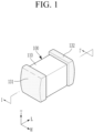
- FIG. 1 is a perspective view illustrating a multilayered capacitor 100 according to an embodiment
- FIG. 2 is a cross-sectional view of the multilayered capacitor 100 taken along line I-I' of FIG. 1
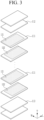
- FIG. 3 is an exploded perspective view illustrating a stacked structure of internal electrode layers in the capacitor body 110 of FIG. 1 .
- the L-axis, W-axis, and T-axis indicated in the drawings represent the longitudinal direction, the width direction, and the thickness direction of the capacitor body 110, respectively.
- the thickness direction (T-axis direction) may be a direction perpendicular to the wide surface (main surface) of the sheet-shaped components, and may be, for example, used in the same concept as the stacking direction in which the dielectric layers 111 are stacked.
- the longitudinal direction (L-axis direction) may be a direction substantially perpendicular to the thickness direction (T-axis direction) in a direction extending parallel to the wide surface (main surface) of the sheet-shaped components, and may be, for example, a direction in which the first and second external electrodes 131 and 132 are disposed.
- the width direction (W-axis direction) may be a direction that extends parallel to the wide surface (main surface) of the sheet-shaped components and is substantially perpendicular to the thickness direction (T-axis direction), and the length of the sheet-like components in the longitudinal direction (L-axis direction) may be longer than the length in the width direction (W-axis direction).
- the multilayered capacitor 100 may include the capacitor body 110, and first and second external electrodes 131 and 132 disposed on both end surfaces of the capacitor body 110 which face each other in the longitudinal direction (L-axis direction).
- the capacitor body 110 may have, for example, a substantially hexahedral shape.
- surfaces opposite to each other in the thickness direction are defined as first and second surfaces
- surfaces connected to the first and second surfaces and facing each other in the longitudinal direction (L-axis direction) are defined as third and fourth surfaces
- surfaces connected to the first and second surfaces, connected to the third and fourth surfaces, and facing each other in the width direction (W-axis direction) are defined as fifth and sixth surfaces.
- the first surface which is a lower surface, may be a surface facing the mounting direction of the multilayered capacitor 100.
- the first to sixth surfaces may be flat, but the present disclosure is not limited thereto, for example, the first to sixth surfaces may be curved surfaces with a convex central portion, and an edge of each surface which is a boundary, may be round.
- the shape and dimensions of the capacitor body 110 and the number of stacked dielectric layers 111 are not limited to those shown in the drawings of the present embodiment.
- the capacitor body 110 is formed by stacking a plurality of the dielectric layers 111 in the thickness direction (T-axis direction) and then firing them, and includes a plurality of dielectric layers 111, and first and second internal electrode layers 121 and 122 which are alternately disposed in a thickness direction (T-axis direction) with the dielectric layers 111 interposed therebetween.
- the boundary between the respective dielectric layers 111 adjacent to each other of the capacitor body 110 may be integrated to the extent that it is difficult to check without using a scanning electron microscope (SEM).
- SEM scanning electron microscope
- the capacitor body 110 may include an active region and cover regions 112 and 113.
- the active region contributes to generating a capacitance of the multilayered capacitor 100.
- the active region may be a region in which the first and second internal electrode layers 121 and 122 are stacked and overlapped with each other along the thickness direction (T-axis direction).
- the cover regions 112 and 113 may be respectively disposed on the first and second surfaces of the active region in the thickness direction (T-axis direction) as thickness-direction margin portions.
- the cover regions 112 and 113 may be formed by stacking a single dielectric layer 111 or two or more dielectric layers 111 on an upper surface and a lower surface of the active region, respectively.
- the capacitor body 110 may further include a side cover region.
- the side cover region is a width-direction margin portion, and may be respectively disposed on the fifth and sixth surfaces of the active region in the width direction (W-axis direction).
- Such side cover regions may be formed by coating a conductive paste layer for forming internal electrode layers on the surface of the dielectric green sheet only on a portion of the surface of the dielectric green sheet, stacking dielectric green sheets on which a conductive paste layer is not coated on both side surfaces of the dielectric green sheet, and firing the same.
- the cover regions 112 and 113 and the side cover regions serve to prevent damage to the first and second internal electrode layers 121 and 122 due to physical or chemical stress.
- the dielectric layer 111 is described in detail.
- the dielectric layer 111 include a plurality of dielectric grains 1111.
- the dielectric grain 1111 includes a main component and a subcomponent.
- the main component may be a dielectric material including a barium titanite-based compound.
- the main component may be a dielectric material including BaTiO 3 , Ba(Ti, Zr)O 3 , Ba(Ti, Sn)O 3 , (Ba, Ca)TiO 3 , (Ba, Ca)(Ti, Zr)O 3 , (Ba, Ca)(Ti, Sn)O 3 , (Ba, Sr)TiO 3 , (Ba, Sr)(Ti, Zr)O 3 , (Ba, Sr)(Ti, Sn)O 3 , or a combination thereof.
- the main component may include Ba m TiO 3 (0.995 ⁇ m ⁇ 1.01), (Ba 1-x Ca x ) m (Ti 1-y Zr y )O 3 (0.995 ⁇ m ⁇ 1.01, 0 ⁇ x ⁇ 0.1, 0 ⁇ y ⁇ 0.2), Ba m (Ti 1-x Zr x )O 3 (0.995 ⁇ m ⁇ 1.01, x ⁇ 0.1), (Ba 1-x Ca x ) m (Ti 1-y Sn y )O 3 (0.995 ⁇ m ⁇ 1.01, 0 ⁇ x ⁇ 0.1, 0 ⁇ y ⁇ 0.2), or combinations thereof.
- the subcomponent may include hafnium (Hf), manganese (Mn), chromium (Cr), silicon (Si), aluminum (Al), magnesium (Mg), tin (Sn), antimony (Sb), germanium (Ge), gallium (Ga), indium (In), or a combination thereof.
- the subcomponent may further include lanthanum (La), yttrium (Y), actinide (Ac), cerium (Ce), praseodymium (Pr), neodymium (Nd), promethium (Pm), samarium (Sm), europium (Eu), gadolinium (Gd), terbium (Tb), dysprosium (Dy), holmium (Ho), erbium (Er), thulium (Tm), ytterbium (Yb), lutetium (Lu), hafnium (Hf), vanadium (V), or combinations thereof.
- La lanthanum
- Y actinide
- Ce cerium
- Pr praseodymium
- Nd neodymium
- Sm promethium
- Sm samarium
- Eu europium
- Gd gadolinium
- Tb terbium
- Dy dysprosium
- Ho holmium
- the subcomponent may include about 0.1 parts by mole to about 1.0 part by mole of Dy 2 O 3 , about 0.1 parts by mole to about 1.0 part by mole of Tb 2 O 3 , about 0 parts by mole to about 0.2 parts by mole of MnO 2 , about 0 parts by mole to about 0.15 parts by mole of V 2 O 5 , about 1.5 parts by mole to about 3.3 parts by mole of BaCO 3 , about 0.5 parts by mole to about 4.0 parts by mole of SiO 2 , about 0.4 parts by mole to about 0.6 parts by mole of Al 2 O 3 , and about 0 parts by mole to about 0.8 parts by mole of CaCO 3 relative to 100 parts by mole of the main component.
- At least one of the plurality of dielectric grains 1111 has a core-shell structure.
- FIG. 4 exhibits the dielectric grain with the core-shell structure.
- the dielectric grain 1111 with the core-shell structure includes a dielectric material core 1111a and a shell 1111b surrounding at least a portion of the core 1111a within one dielectric grain 1111.
- the core 1111a and the shell 1111b have a different molar ratio of a subcomponent to a main component, for example, the molar ratio of the subcomponent to the main component may sharply change at the boundary between the core 1111a and the shell 1111b. Accordingly, the boundary between the core 1111a and the shell 1111b may be easily distinguished, which may be determined through transmission electron microscope-energy dispersive X-ray analysis (TEM-EDX).
- TEM-EDX transmission electron microscope-energy dispersive X-ray analysis
- the core 1111a and the shell 1111b may be distinguished by the boundary of the core 1111a and the shell 1111b where a total content of the subcomponent starts to sharply increase from the center of the core 1111a of the dielectric grain 1111 toward any boundary direction of the dielectric grain 1111.
- the center of the core 1111a may be determined as a point where the largest major axis of the core 1111a meets the largest minor axis among minor axes perpendicular thereto.
- the EDS (energy disperse X-ray spectrometer) line analysis may be performed along the major axis passing through the center of the core 1111a of the dielectric grain 1111.
- the boundary between the shell (S) and the grain boundary (GB) may be defined by dividing portions with a different contrast in a method binarizing the transmission electron microscope image and the like.
- the core 1111a may include less than or equal to about 0.1 parts by mole of the subcomponent based on about 100 parts by mole of the main component
- the shell 1111b may include greater than about 0.1 parts by mole and less than or equal to about 30.0 (or about 30) parts by mole or greater than about 0.1 parts by mole and less than or equal to about 20.0 parts by mole (or about 20 parts by mole) of the subcomponent based on about 100 parts by mole of the main component.
- the shell 1111b may include greater than about 0.1, 0.2, 0.3, 0.4, 0.5, 0.6, 0.7, 0.8, 0.9 or 1 parts by mole and less than or equal to about 30, 29, 28, 27, 26, 25, 24, 23, 22, 21, 20 parts by mole of the subcomponent based on about 100 parts by mole of the main component.
- the core 1111a includes greater than about 0.1 parts by mole of the subcomponent based on about 100 parts by mole of the main component, material characteristics of a pure dielectric material (i.e., BaTiOs) may be changed, and when the shell 1111b includes less than or equal to about 0.1 parts by mole of the subcomponent based on about 100 parts by mole of the main component, a dielectric constant according to a temperature may greatly be changed, and when greater than about 30.0 parts by mole of the subcomponent is included, initial insulation resistance may be lowered.
- a pure dielectric material i.e., BaTiOs
- the shell 1111b may include greater than about 0.1 parts by mole and less than or equal to about 4.5 parts by mole of the subcomponent based on about 100 parts by mole of the main component. In some embodiments, the shell 1111b may include greater than about 0.1, 0.2, 0.3, 0.4, 0.5, 0.6, 0.7, 0.8, 0.9 or 1 parts by mole and less than or equal to about 4.5, 4.4, 4.3, 4.2, 4.1, 4, 3.9, 3.8, 3.7, 3.6, 3.5 parts by mole of the subcomponent based on about 100 parts by mole of the main component.
- the core 1111a may include a pure main component alone without impurities, wherein the pure main component may in general have a high dielectric constant, compared with a main component doped with impurity elements. Accordingly, the core 1111a plays a role of maintaining a dielectric constant.
- An amount of the subcomponent(s) included in the shell 1111b may be more than the amount of the subcomponent(s) included in the core 1111a.
- the subcomponent doped at a B-site of the main component may have an effect of increasing band gap energy in which other rare earth elements and doping elements diffuse into the dielectric grain 1111. Accordingly, the subcomponent may serve as a barrier to suppress the diffusion of the other rare earth elements and the doping elements into the dielectric grains 1111.
- the shell 1111b may serve to suppress growth of the dielectric grain 1111, thereby contributing to atomization of the dielectric grain 1111.
- the subcomponent doped onto an A-site of the main component may serve to improve reliability and a dielectric constant.
- a diameter of the core is about 60% to about 80% of a diameter of the dielectric grain with the core-shell structure.
- D grain the diameter of the core
- D core a ratio thereof is calculated according to calculation equation (D core /D grain ⁇ 100), which may be expressed as a core fraction, a core length fraction, or the like.
- the diameter of the dielectric grain with the core-shell structure and the diameter of the core may be obtained by randomly selecting about 50 grains from an image of the dielectric layer taken with a scanning electron microscope to measure the diameters of the grains and the diameter of the cores and then calculate their arithmetic averages. For example, a cross-section of a main-fired MLCC chip is exposed to take a photograph of three layers of an active center of an active region with SEM and then from the 70K magnification image, each diameter of 50 grains and 50 cores therein are measured and an arithmetic mean is calculated.
- the SEM analysis is performed by setting an acceleration voltage at about 2.0 kV and WD at about 3.2 mm.
- the diameters may be calculated as an average of a max feret diameter and an orthogonal feret diameter.
- the diameter of the dielectric grain, the diameter of the core, etc. may be expressed as an average diameter.
- the present embodiment has used a liquid metal oxide additive rather than an oxide additive during manufacturing of the dielectric grain to induce the elements to be uniformly distributed around the core without forming agglomerates and also secured an optimal core fraction through sintering after changing a content of the liquid metal oxide additive alone, while maintaining the same composition of the liquid metal oxide additive.
- the content of the liquid metal oxide additive serving as a type of the subcomponent or a dopant is reduced at a predetermined rate, while keeping compositions of the raw materials and conditions such as a firing temperature and the like the same, the core length fraction in the dielectric grain may be dramatically increased.
- the aforementioned core fraction may be about 60% to about 80%, for example about 60% to about 76%, or about 70% to about 80%, or about 74.5% to about 80%.
- the core fraction that is, the ratio of the diameter of the core to that of the dielectric grain satisfies the ranges, overall performance of the multilayered capacitor such as voltage withstand characteristics, a dielectric constant, DC characteristics, temperature stability, and the like may be improved.
- a diameter of the dielectric grains of the core-shell structure may be about 100 nm to about 1,000 nm, and specifically about 300 nm to about 500 nm, or about 340 nm to about 440 nm. Additionally, the diameter of the core 1111a may be about 50 nm to about 500 nm, and more specifically about 200 nm to about 400 nm, or about 240 nm to about 340 nm. In this case, capacity characteristics and reliability of the multilayered capacitor may be improved.
- the dielectric grains of the core-shell structure according to the present embodiment is characterized in that the thickness of the shell 1111b is constant, i.e., a deviation of the shell thickness is small, since it is manufactured using a liquid metal oxide additive.
- a standard deviation of an average thickness of the shell 1111b may be less than or equal to about 10%, or less than or equal to about 5% relative to the diameter of the dielectric grains of the core-shell structure. In this case, voltage withstand characteristics of the multilayered capacitor may be greatly improved.
- an average thickness of the dielectric layer 111 may be about 0.2 ⁇ m to about 10 ⁇ m, or about 0.4 ⁇ m to about 1 ⁇ m.
- the first and second internal electrodes 121 and 122 are electrodes having different polarities, and are alternately disposed to face each other along the T-axis direction with the dielectric layer 111 interposed therebetween, and one end thereof may be exposed through the third and fourth surfaces of the capacitor body 110.
- the first and second internal electrodes 121 and 122 may be electrically insulated from each other by the dielectric layer 111 disposed in the middle.
- Ends of the first and second internal electrodes 121 and 122 alternately exposed through the third and fourth surfaces of the capacitor body 110 are connected to the first and second external electrodes 131 and 132, respectively, to be electrically connected.
- the first and second internal electrode layers 121 and 122 may include a conductive metal, for example, a metal such as Ni, Cu, Ag, Pd, or Au, and the like, an alloy thereof, for example an Ag-Pd alloy.
- a conductive metal for example, a metal such as Ni, Cu, Ag, Pd, or Au, and the like, an alloy thereof, for example an Ag-Pd alloy.
- first and second internal electrode layers 121 and 122 may include dielectric particles having the same composition as the ceramic material included in the dielectric layer 111.
- the first and second internal electrode layers 121 and 122 may be formed using a conductive paste containing a conductive metal.
- a method of printing the conductive paste a screen-printing method or a gravure printing method or the like may be used.
- each average thickness of the first and second internal electrode layers 121 and 122 may be about 0.1 ⁇ m to about 2 ⁇ m.
- the first and second external electrodes 131 and 132 are supplied with voltages of different polarities, and are electrically connected to exposed portions of the first and second internal electrodes 121 and 122, respectively.
- a capacitance of the multilayered capacitor 100 is proportional to an overlapping area of the first and second internal electrodes 121 and 122 overlapping each other along the T-axis direction in the active region.
- the first and second external electrodes 131 and 132 may respectively include a first connection portion and a second connection portion disposed on the third and fourth surfaces of the capacitor body 110 and connected to the first and second internal electrodes 121 and 122, and may also include a first band portion and a second band portion disposed at each corner where the third and fourth surface and the first and second surfaces or the fifth and sixth surfaces of the capacitor body 110 meet.
- the first and second band portions may extend from the first and second connection portions to portions of the first and second surfaces or the fifth and sixth surfaces of the capacitor body 110, respectively.
- the first and second band portions may serve to improve adhesion strength of the first and second external electrodes 131 and 132.
- the first and second external electrodes 131 and 132 may each include a sintered metal layer in contact with the capacitor body 110, a conductive resin layer configured to cover the sintered metal layer, and a plating layer configured to cover the conductive resin layer.
- the sintered metal layer may include a conductive metal and glass.
- the sintered metal layer may include copper (Cu), nickel (Ni), silver (Ag), palladium (Pd), gold (Au), platinum (Pt), tin (Sn), tungsten (W), titanium (Ti), lead (Pb), an alloy thereof, or a combination thereof, as a conductive metal, and for example the copper (Cu) may include a copper (Cu) alloy.
- the conductive metal includes copper
- a metal other than copper may be included in an amount of less than or equal to about 5 parts by mole based on 100 parts by mole of copper.
- the sintered metal layer may include a composition of oxides as a glass, for example, one or more selected from a silicon oxide, a boron oxide, an aluminum oxide, a transition metal oxide, an alkali metal oxide, and an alkaline earth metal oxide.
- the transition metal may be selected from zinc (Zn), titanium (Ti), copper (Cu), vanadium (V), manganese (Mn), iron (Fe), and nickel (Ni);
- the alkali metal may be selected from lithium (Li), sodium (Na), and potassium (K); and the alkaline-earth metal may be selected from magnesium (Mg), calcium (Ca), strontium (Sr), and barium (Ba).
- Contents of the conductive metal and glass in the sintered metal layer are not particularly limited, but for example, an average area of the conductive metal in a cross section perpendicular to the thickness direction (W-axis direction) of the multilayered capacitor 100 (L-axis and T-axis direction sections) may be about 30% to about 90%, or about 70% to about 90%, of the total area of the sintered metal layer.
- the conductive resin layer may include the sintered metal layer, for example, completely covering the sintered metal layer.
- the first and second external electrodes 131 and 132 may not include a sintered metal layer, in which case the conductive resin layer may be in direct contact with the capacitor body 110.
- the conductive resin layer extends to the first and second surfaces or the fifth and sixth surfaces of the capacitor body 110, wherein a region (i.e., a band portion) where the conductive resin layer extends to the first and second surfaces or the fifth and sixth surfaces of the capacitor body 110 may have a longer length than a region (i.e., band portion) where the sintered metal layer extends the first and second surfaces or the fifth and sixth surfaces of the capacitor body 110.
- the conductive resin layer is formed on the sintered metal layer, while fully covering the sintered metal layer.
- the conductive resin layer may include a resin and a conductive metal.
- the resin included in the conductive resin layer is not particularly limited as long as it has bondability and impact absorption properties and can be mixed with the conductive metal powder to form a paste, and may include, for example, a phenolic resin, an acrylic resin, a silicone resin, an epoxy resin, or a polyimide resin.
- the conductive metal included in the conductive resin layer may serve to electrically connect the first and second internal electrodes 121 and 122 or the sintered metal layer.
- the conductive metal included in the conductive resin layer may have a spherical shape, a flake shape, or a combination thereof. That is, the conductive metal may be formed only in a flake shape, only in a spherical shape, or may have a mixed shape of a flake shape and a spherical shape.
- the spherical shape may also include a shape that is not perfectly spherical, and may include a shape in which, for example, a length ratio between a major axis and a minor axis (long axis/short axis) is less than or equal to about 1.45.
- the flake-shaped powder means a powder having a flat and elongated shape, and is not particularly limited, but, for example, a length ratio between a major axis and a minor axis (long axis/short axis) may be greater than or equal to about 1.95.
- the first and second external electrodes 131 and 132 may further include a plating layer outside the conductive resin layer.
- the plating layer may include nickel (Ni), copper (Cu), tin (Sn), palladium (Pd), platinum (Pt), gold (Au), silver (Ag), tungsten (W), titanium (Ti), or lead (Pb), alone or an alloy thereof.
- the plating layer may be a nickel (Ni) plating layer or a tin (Sn) plating layer, and may have a form in which a nickel (Ni) plating layer and a tin (Sn) plating layer are sequentially stacked or a tin (Sn) plating layer, a nickel (Ni) plating layer, and a tin (Sn) plating layer are sequentially stacked.
- the plating layer may include a plurality of nickel (Ni) plating layers and/or a plurality of tin (Sn) plating layers.
- the plating layer may improve mountability of the multilayered capacitor 100 with a board, structural reliability, external durability, heat resistance, and equivalent series resistance (ESR).
- ESR equivalent series resistance
- a method of manufacturing a multilayered capacitor according to an aspect includes mixing a ceramic powder and a liquid metal oxide additive to prepare a dielectric paste including dielectric grains of the core-shell structure, manufacturing a dielectric green sheet using the dielectric paste, forming a conductive paste layer on a surface of the dielectric green sheet, stacking the dielectric green sheet with the conductive paste layer to manufacture a dielectric green sheet stack, firing the dielectric green sheet stack to manufacture a capacitor body, and forming an external electrode on a first surface of the capacitor body.
- the liquid metal oxide additive is added in an amount of about 0.05 parts by mole to about 4.5 parts by mole based on 100 parts by mole of the ceramic powder.
- the ceramic powder may include a barium titanite-based compound, and specifically, BaTiO 3 , Ba(Ti, Zr)O 3 , Ba(Ti, Sn)O 3 , (Ba, Ca)TiO 3 , (Ba, Ca)(Ti, Zr)O 3 , (Ba, Ca)(Ti, Sn)O 3 , (Ba, Sr)TiO 3 , (Ba, Sr)(Ti, Zr)O 3 , (Ba, Sr)(Ti, Sn)O 3 , or a combination thereof.
- BaTiO 3 Ba(Ti, Zr)O 3 , Ba(Ti, Sn)O 3 , Ba(Ti, Sn)O 3 , (Ba, Ca)(Ti, Sn)O 3 , or a combination thereof.
- the ceramic powder may include Ba m TiO 3 (0.995 ⁇ m ⁇ 1.01), (Ba 1-X Ca x ) m (Ti 1-y Zr y )O 3 (0.995 ⁇ m ⁇ 1.01, 0 ⁇ x ⁇ 0.1, 0 ⁇ y ⁇ 0.2), Ba m (Ti 1-x Zr x )O 3 (0.995 ⁇ m ⁇ 1.01, x ⁇ 0.1), (Ba 1-X Ca x ) m (Ti 1-y Sn y )O 3 (0.995 ⁇ m ⁇ 1.01, 0 ⁇ x ⁇ 0.1, 0 ⁇ y ⁇ 0.2), or a combination thereof.
- the liquid metal oxide additive may be a type of subcomponent raw material or dopant raw material.
- the liquid metal oxide additive may be prepared by adding metal oxide powder to an acidic solvent, so that the metal oxide may exist in an ionized state in the additive.
- the liquid metal oxide additive may include the acidic solvent and ionic metal oxide or may include an organic salt of the metal oxide.
- the organic salt of the metal oxide may be a resulting material of an ion reaction between the ionic metal oxide and an ionic surfactant.
- the acidic solvent may include, for example, hydrochloric acid, nitric acid, oxalic acid, hydrogen peroxide, or a combination thereof but is not limited thereto.
- the metal oxide, the ionic metal oxide and the organic salt of the metal oxide may include manganese (Mn), chromium (Cr), silicon (Si), aluminum (Al), magnesium (Mg), tin (Sn), antimony (Sb), germanium (Ge), gallium (Ga), indium (In), or a combination thereof as a metal element, and may further include lanthanum (La), yttrium (Y), actinide (Ac), cerium (Ce), praseodymium (Pr), neodymium (Nd), promethium (Pm), samarium (Sm), europium (Eu), gadolinium (Gd), terbium (Tb), dysprosium (Dy), holmium (Ho), erbium (Er), thulium (Tm), ytterbium (Yb), lutetium (Lu), hafnium (Hf), vanadium (V), or a combination thereof.
- the metal oxide may include about 0.1 parts by mole to about 1.0 part by mole of Dy 2 O 3 , about 0.1 parts by mole to about 1.0 part by mole of Tb 2 O 3 , about 0 parts by mole to about 0.2 parts by mole of MnO 2 , about 0 parts by mole to about 0.15 parts by mole of V 2 O 5 , about 1.5 parts by mole to about 3.3 parts by mole of BaCO 3 , about 0.5 parts by mole to about 4.0 parts by mole of SiO 2 , about 0.4 parts by mole to about 0.6 parts by mole of Al 2 O 3 , and/or about 0 parts by mole to about 0.8 parts by mole of CaCO 3 based on 100 parts by mole of the ceramic powder.
- a conventional technology of using a particle-type oxide additive may hardly realize intended characteristics of a capacitor due to deteriorated dispersibility of the additive and deteriorated thickness uniformity of a shell according to aggregation of the additive.
- the dispersibility may be improved without separately using a dispersant, and the added elements are uniformly dispersed around the core without forming agglomerates, manufacturing dielectric grains with excellent quality and resultantly, improving overall performance of a multilayered capacitor such as voltage withstand characteristics and the like
- the content of the additive may be changed, while maintaining the same composition of the additive and then sintered to control the core-shell fraction in the dielectric grain.
- the liquid metal oxide additive should be used.
- the dielectric grains have a core-shell structure, and a dielectric constant and voltage withstand characteristics, DC characteristics, a temperature coefficient of capacitance (TCC) greatly vary depending on a core-shell ratio thereof, it is important to realize an appropriate core-shell ratio.
- the embodiment has succeeded in reducing a shell ratio but increasing a relative core ratio by maintaining each element in the same ratio in the liquid metal oxide additive but changing a content of the liquid metal oxide additive alone in and also, maintaining the same firing condition. For example, when the content of the liquid metal oxide additive with the same composition is reduced from about 100% to about 62.5%, the core fraction may increase from about 55% to about 76%, and this method may control the core fraction within a range of about 60% to about 80%.
- the content of the liquid metal oxide additive may be reduced to less than or equal to about 90%, for example less than or equal to about 80%, or less than or equal to about 70%, or about 60% to about 90% to increase the core fraction, which is the ratio of the core diameter to the grain diameter, wherein the core fraction is controlled to about 60% to about 80%, all improving a dielectric constant, voltage withstand characteristics, DC characteristics, TCC characteristics of the multilayered capacitor.
- the liquid metal oxide additive may be added in an amount of about 0.05 parts by mole to about 4.5 parts by mole, for example 0.1 parts by mole to 4.0 parts by mole, or 1.0 part by mole to 3.5 parts by mole based on 100 parts by mole of the ceramic powder.
- the core fraction may be controlled to about 60% to about 80%, which may improve a dielectric constant, voltage withstand characteristics, DC characteristics, and TCC characteristics of the multilayered capacitor.
- a solvent, a plasticizer, a binder, and the like may be mixed together. After the mixing, the mixture may be filtered, condensed, or dried, preparing a dielectric paste.
- a dielectric green sheet is obtained by forming the obtained dielectric paste into a sheet by a doctor blade method or the like.
- the dielectric paste may include an additive selected from various dispersants, plasticizers, dielectrics, subcomponent compounds, or glass as needed.
- the conductive paste include the composition that becomes the internal electrode after firing.
- Conductive paste for the internal electrode may be prepared by kneading conductive powder made of a conductive metal or an alloy thereof with a binder or a solvent.
- the conductive paste for the internal electrode may include ceramic powder (for example, barium titanate powder) as a co-material, if necessary.
- the co-material may act to suppress sintering of the conductive powder during the firing process.
- the conductive paste for an internal electrode is applied in a predetermined pattern by various printing methods such as screen printing or a transfer method. After stacking a plurality of layers of dielectric green sheets on which internal electrode patterns are formed, a dielectric green sheet stack is obtained by pressing in the stacking direction. At this time, the dielectric green sheets and internal electrode patterns may be stacked so that the dielectric green sheets may be disposed on the upper and lower surfaces of the dielectric green sheet stack in the stacking direction.
- the obtained dielectric green sheet stack may be cut into predetermined dimensions by dicing or the like.
- the dielectric green sheet stack may be solidified and dried to remove the plasticizer, etc. and barrel-polished by using a centrifugal barrel machine or the like after the solidification-drying.
- the dielectric green sheet stack is put with a medium and a polishing liquid into a barrel container, and then the barrel container is applied with rotational motion or vibration to polish unnecessary parts such as burrs and the like generated during the cutting.
- the dielectric green sheet stack is washed with a cleaning solution such as water and the like and dried.
- the dielectric green sheet stack may be treated to remove the binder and fired, obtaining the capacitor body.
- the binder removal may be performed under conditions appropriately adjusted according to a main component composition of the dielectric layer or a main component composition of the internal electrode.
- the binder removal may be performed by increasing a temperature at about 5 °C/hr to about 300 °C/hr and maintaining about 180 °C to about 400 °C for about 0.5 hours to about 24 hours.
- the binder removal may be performed under an air atmosphere or a reducing atmosphere.
- the firing treatment may be performed under conditions appropriately adjusted according to the main component composition of the dielectric layer or the main component composition of the internal electrode.
- the firing may be performed at about 1000 °C to about 1350 °C or about 1100 °C to about 1300 °C for about 0.5 hours to about 8 hours or about 1 hour to about 3 hours.
- the firing may be performed under a reducing atmosphere, for example, an atmosphere in which a mixed gas of nitrogen gas (N 2 ) and hydrogen gas (H 2 ) is humidified.
- N 2 nitrogen gas
- H 2 hydrogen gas
- an oxygen partial pressure may be about 1.0 ⁇ 10 -14 MPa to about 1.0 ⁇ 10 -10 MPa under the firing atmosphere.
- annealing may be performed, if needed.
- the annealing is performed for re-oxidizing the dielectric layer, and when the firing is performed under a reducing atmosphere, the annealing may be performed.
- the annealing may be performed under conditions appropriately adjusted according to the main component composition and the like of the dielectric layer. For example, the annealing may be performed at about 950 °C to about 1150 °C for about 0 hour to about 20 hours by increasing the temperature at about 50 °C/hour to about 500 °C/hour.
- the annealing may be performed under a humid nitrogen gas (N 2 ) atmosphere, wherein an oxygen partial pressure may be about 1.0 ⁇ 10 -9 MPa to about 1.0 ⁇ 10 -5 MPa.
- N 2 humid nitrogen gas
- a wetter or the like may be for example, used, wherein a water temperature may be about 5 °C to about 75 °C.
- the binder removal treatment, the firing treatment, and the annealing treatment may be performed continuously or independently.
- the third and fourth surfaces of the obtained capacitor body may be surface-treated through sandblasting, laser irradiation, barrel polishing, or the like.
- This surface treatment may expose the ends of the first and second internal electrodes on the outer surfaces of the third and fourth surfaces, thereby improving the electrical connection of the first and second external electrodes and the first and second internal electrodes and easily forming an alloy portion.
- a paste for forming a sintered metal layer is coated and sintered to form a sintered metal layer.
- the paste for forming the sintered metal layer may include a conductive metal and glass.
- the conductive metal and the glass are the same as described above and will not be repeated illustrated again.
- the paste for forming the sintered metal layer may optionally include a subcomponent such as a binder, a solvent, a dispersant, a plasticizer, or oxide powder.
- the binder may include ethyl cellulose, acryl, butyral, or the like
- the solvent may use an organic solvent such as terpineol, butyl carbitol, alcohol, methylethylketone, acetone, or toluene, or an aqueous solvent.
- a method of coating the paste for forming the sintered metal layer on the outer surface of the capacitor body may include various printing methods such as a dip method, or screen printing, and the like, a coating method by using a dispenser, a spray method by using a spray, and the like.
- the paste for the sintered metal layer may be coated on at least the third and fourth surfaces of the capacitor body, and optionally, on a portion of the first surface, the second surface, the fifth surface, or the sixth surface where the band portions of the first and second external electrodes are formed
- the capacitor body on which the paste for forming the sintered metal layer is coated is dried and then sintered at a temperature of about 700 °C to about 1000 °C for about 0.1 hour to about 3 hours to form a sintered metal layer.
- a paste for forming a conductive resin layer is coated and cured to form a conductive resin layer.
- the paste for forming the conductive resin layer may include a resin, and optionally a conductive metal or a non-conductive filler.
- the conductive metal and resin are the same as described above and will not be repeated illustrated again.
- the paste for forming the conductive resin layer may optionally include a subcomponent such as a binder, a solvent, a dispersant, a plasticizer, or an oxide powder.
- the binder may include ethyl cellulose, acryl, butyral, or the like
- the solvent may include an organic solvent such as terpineol, butyl carbitol, alcohol, methylethylketone, acetone, or toluene, and the like or an aqueous solvent.
- a method of forming the conductive resin layer may include dipping the capacitor body 110 into the paste for forming the conductive resin layer to form the conductive resin layer and curing it, screen-printing or gravure-printing the paste for forming the conductive resin layer on the surface of the capacitor body 110, or coating the paste for forming the conductive resin layer on the surface of the capacitor body 110 and then curing it.
- the plating layer is formed outside the conductive resin layer.
- the plating layer may be formed by a plating method, or may be formed by sputtering or electroplating (electric deposition).
- the ceramic powder may include BaTiOs powder.
- a liquid metal oxide additive was prepared by adding 0.1 to 1.0 parts by mole of Dy 2 O 3 , 0.1 to 1.0 parts by mole of Tb 2 O 3 , 0 to 0.2 parts by mole of MnO 2 , 0 to 0.15 parts by mole of V 2 O 5 , 1.5 to 3.3 parts by mole of BaCO 3 , 0.5 to 4.0 parts by mole of SiO 2 , 0.4 to 0.6 parts by mole of Al 2 O 3 , and 0 to 0.8 parts by mole of CaCO 3 based on 100 parts by weight of the ceramic powder to a distilled water solvent and then mixing them, and filtering and drying the mixture.
- the liquid metal oxide additive was mixed with the ceramic powder in a distilled water solvent and then mechanically milled, preparing a dielectric paste.
- 5 parts by mole of the liquid metal oxide additive was used based on 100 parts by mole of the ceramic powder (Comparative Example 1).
- the content of the liquid metal oxide additive in Comparative Example 1 was respectively reduced to 88.6 mol% (Example 1), 75 mol% (Example 2), and 62.5 mol% (Example 3), preparing each dielectric paste.
- the metal oxide additives are controlled to have the same composition.
- the prepared dielectric paste was processed through a head discharge-type on-roll molding coater, manufacturing a dielectric green sheet.
- the dielectric green sheet stack was calcined at less than or equal to 400 °C under a nitrogen atmosphere and sintered at 1180 °C under a hydrogen concentration of 1.0% or less, manufacturing a multilayered capacitor.
- the multilayered capacitors according to Comparative Example 1 and Examples 1 to 3 were polished to a depth of 1/2 in the width direction to expose an LT cross-section and then to take a photograph of three dielectric green sheet layers of an active center in an active region with a scanning electron microscope (SEM), from which dielectric grains are analyzed. SEM was set at an accelerating voltage of 2.0 kV and WD of 3.2 mm.
- FIG. 5 is a 70K magnification SEM image of the dielectric grains of Comparative Example 1 and Examples 2 and 3, wherein the upper images exhibit a boundary of each grain, and the lower images exhibit each core therein.
- the SEM images show that core portions inside the grains are clearly distinguished, and as the content of the additive is reduced, the shell ratio decreases, but the core ratio increases.
- the content of the additive was reduced, since the elements of the additive were decreasingly diffused from the surface of the ceramic powder to the inside, the shell ratio decreases, thereby increasing the core fraction.
- a conventional oxide additive was used, since polydispersity of the additive is much reduced, the additive is partially agglomerated, making it difficult to realize intended characteristics of a capacitor.
- the shell ratio may be reduced, while still keeping a uniform thickness of the shell.
- Example 1 Content of additive (wt%) D grain (nm) Dcore (nm) Core length fraction (D core /D grain ) Comparative Example 1 100 391.45 214.28 54.7%
- Example 2 75 423.66 315.56 74.5%
- Example 3 62.5 398.79 302.91 76.0%
- the multilayered capacitors according to Comparative Example 1 and Examples 1 to 3 were evaluated with respect to a dielectric constant and DC-bias characteristics, and the results are shown in Table 2.
- the multilayered capacitors according to Comparative Example 1 and Example 2 were measured with respect to a change in a dielectric constant according to a temperature, and the results are shown in Table 3.
- the examples of increasing a core fraction exhibited an increase in the dielectric constant, a decrease in dielectric constant reduction rate when a DC voltage is applied thereto, and improved dielectric characteristics (TCC) according to a temperature, compared with the comparative example.
- the metal oxide further includes lanthanum (La), yttrium (Y), actinide (Ac), cerium (Ce), praseodymium (Pr), neodymium (Nd), promethium (Pm), samarium (Sm), europium (Eu), gadolinium (Gd), terbium (Tb), dysprosium (Dy), holmium (Ho), erbium (Er), thulium (Tm), ytterbium (Yb), lutetium (Lu), hafnium (Hf), vanadium (V), or a combination thereof.
- La lanthanum
- Y actinide
- Ce cerium
- Pr praseodymium
- Nd neodymium
- Pm promethium
- Sm samarium
- Eu europium
- Gd gadolinium
- Tb terbium
- Dy dysprosium
- Ho holmium
Landscapes
- Engineering & Computer Science (AREA)
- Power Engineering (AREA)
- Manufacturing & Machinery (AREA)
- Microelectronics & Electronic Packaging (AREA)
- Chemical & Material Sciences (AREA)
- Ceramic Engineering (AREA)
- Inorganic Chemistry (AREA)
- Ceramic Capacitors (AREA)
- Fixed Capacitors And Capacitor Manufacturing Machines (AREA)
Abstract

Description
- A multilayered capacitor and a manufacturing method thereof are disclosed.
- Recently, development of automotive electrical device parts has been rapidly progressing. A multilayered capacitor (MLCC), one of the electrical device parts, has an advantage of being small but capable of high capacity and thus is used as a part of various electronic products.
- Performance of the multilayered capacitor is determined by a dielectric constant, voltage withstand characteristics, temperature characteristics, reliability, and the like. The multilayered capacitor has a dielectric layer formed by adding a predetermined amount of various types of additives to ceramic powder, and when the dielectric layer is based on a barium titanite, the performance of the multilayered ceramic capacitor may be improved by controlling a microstructure such as a dielectric grain size, a core size, a concentration of a shell, etc. or defect behaviors such as oxygen defects.
- Regarding the microstructure control, when the dielectric grain size is increased, the dielectric constant may increase, but there are problems of deteriorating the voltage withstand characteristics and high temperature characteristics due to a grain ratio decrease and a shell ratio increase in the dielectric layer. In order to solve the problems, since the particle size has to inevitably be reduced, which may cause a side effect of decreasing the dielectric constant, in order to mitigate this side effect, research needs to be conducted toward maintaining the core size at a predetermined level, while still reducing the grain size.
- In order to control the defect behaviors, a donner and an acceptor in an appropriate ratio are required to be dopped. The donner, based on barium titanite-based ceramics, may be mainly rare earth materials. The rare earth doping has a very large effect on characteristic changes of the barium titanite-based ceramics and in particular, brings about various effects such as improving a voltage withstand characteristic, a dielectric constant when a DC voltage is applied, temperature stability, and the like. Accordingly, technology of controlling a core/shell ratio and a concentration in the dielectric layer may mainly serve to improve performance of a ceramic capacitor.
- Conventional efforts of increasing the dielectric constant of the dielectric layer have been made by proposing a method of using a parent material with a large grain size in order to increase a core fraction in a dielectric grain with a core-shell structure or by researching on increasing the grain size, as firing time increases, which leads to decreasing the core fraction. However, as MLCC is gradually smaller and thinner, since development of dielectric grains also are being made toward getting smaller, there are limitations in using the parent material with a large grain size or adjusting the firing time.
- Performance of multilayered capacitors, such as a dielectric constant, a voltage withstand characteristic, a dielectric constant under DC voltage application, and temperature stability may be improved by controlling a core-shell fraction of dielectric grains.
- A multilayered capacitor according to one aspect includes a capacitor body including a dielectric layer and an internal electrode, and an external electrode disposed on an outer surface of the capacitor body, wherein the dielectric layer includes a plurality of dielectric grains, at least one of the plurality of dielectric grains has a core-shell structure, and in the dielectric grains having the core-shell structure, a ratio between diameters of the core to the dielectric grain is about 60% to about 80%.
- The ratio of a diameter of the core of the core-shell structure to a diameter of the dielectric grain having the core-shell structure may be about 60% to about 76%, or about 70% to about 80%, or about 74.5% to about 80%.
- A diameter of the dielectric grains having the core-shell structure may be about 300 nm to about 500 nm, and a diameter of the core may be about 200 nm to about 400 nm.
- A standard deviation of an average thickness of the shell may be less than or equal to about 10% relative to the diameter of the dielectric grains of the core-shell structure.
- The dielectric grains may include a main component comprising a barium titanate-based compound and a subcomponent comprising manganese (Mn), chromium (Cr), silicon (Si), aluminum (Al), magnesium (Mg), tin (Sn), antimony (Sb), germanium (Ge), gallium (Ga), indium (In), or combinations thereof.
- In the dielectric grains of the core-shell structure, the shell may include the subcomponent in an amount of greater than about 0.1 moles and less than or equal to about 30.0 moles relative to 100 moles of the main component, and the core may include the subcomponent in an amount of less than or equal to about 0.1 moles relative to 100 moles of the main component.
- For example, the main component may include BaTiO3, Ba(Ti, Zr)O3, Ba(Ti, Sn)O3, (Ba, Ca)TiO3, (Ba, Ca)(Ti, Zr)O3, (Ba, Ca)(Ti, Sn)O3, (Ba, Sr)TiO3, (Ba, Sr)(Ti, Zr)O3, (Ba, Sr)(Ti, Sn)O3, or a combination thereof. Specifically, the main component may include BamTiO3(0.995≤m≤1.01), (Ba1-XCax)m(Ti1-yZry)O3 (0.995≤m≤1.01, 0≤x≤0.10, 0<y≤0.2), Bam(Ti1-xZrx)O3 (0.995≤m≤1.010, 0≤x≤0.10), (Ba1-XCax)m(Ti1-ySny)O3 (0.995≤m≤1.01, 0≤x≤0.1, 0<y≤0.2), or a combination thereof.
- The subcomponent may further include lanthanum (La), yttrium (Y), actinide (Ac), cerium (Ce), praseodymium (Pr), neodymium (Nd), promethium (Pm), samarium (Sm), europium (Eu), gadolinium (Gd), terbium (Tb), dysprosium (Dy), holmium (Ho), erbium (Er), thulium (Tm), ytterbium (Yb), lutetium (Lu), hafnium (Hf), vanadium (V), or combinations thereof.
- The dielectric grains may include, for example, about 0.1 parts by mole to about 1.0 part by mole of Dy2O3, about 0.1 parts by mole to about 1.0 part by mole of Tb2O3, about 0 parts by mole (or more than 0 parts by mole) to about 0.2 parts by mole of MnO2, about 0 parts by mole (or more than 0 parts by mole) to about 0.15 parts by mole of V2O5, about 1.5 parts by mole to about 3.3 parts by mole of BaCO3, about 0.5 parts by mole to about 4.0 parts by mole of SiO2, about 0.4 parts by mole to about 0.6 parts by mole of Al2O3, and about 0 parts by mole (or more than 0 parts by mole) to about 0.8 parts by mole of CaCO3 as a subcomponent relative to 100 parts by mole of the main component.
- An average thickness of the dielectric layer may be about 0.2 µm to about 10 µm.
- A method of manufacturing a multilayered capacitor according to one aspect includes mixing a ceramic powder and a liquid metal oxide additive to prepare a dielectric paste including dielectric grains of the core-shell structure, manufacturing a dielectric green sheet using the dielectric paste, and forming a conductive paste layer on a surface of the dielectric green sheet, stacking the dielectric green sheet with the conductive paste layer to manufacture a dielectric green sheet stack, firing the dielectric green sheet stack to manufacture a capacitor body, and forming an external electrode on a first surface of the capacitor body. Herein, in the preparing of the dielectric paste, the liquid metal oxide additive is added in an amount of about 0.05 parts by mole to about 4.5 parts by mole based on 100 parts by mole of the ceramic powder.
- The liquid metal oxide additive may include an acidic solvent and an ionic metal oxide, and optionally an ionic surfactant.
- The ceramic powder may include barium titanate, and the metal oxide may include manganese (Mn), chromium (Cr), silicon (Si), aluminum (Al), magnesium (Mg), tin (Sn), antimony (Sb), germanium (Ge), gallium (Ga), indium (In), or a combination thereof.
- The multilayered capacitor has improved performance such as a dielectric constant, a voltage withstand characteristic, a dielectric constant under DC voltage application, temperature stability, and the like.
-
-
FIG. 1 is a perspective view of a multilayered capacitor according to an embodiment. -
FIG. 2 is a cross-sectional view of a multilayered capacitor cut along line I-I' ofFIG. 1 . -
FIG. 3 is an exploded perspective view showing a stacked structure of the internal electrode layers in the capacitor body ofFIG. 1 . -
FIG. 4 is a view of a dielectric grain of the core-shell structure, showing a diameter of the dielectric grain (Dgrain) and a diameter of the core (Dcore). -
FIG. 5 shows scanning electron microscope (SEM) images of core-shell dielectric grains of Comparative Example 1, Example 2, and Example 3, from left to right, wherein the top row shows rims of the grains and the bottom row shows the core portions. -
FIG. 6 is a graph showing the core fraction as a function of the content of the liquid metal oxide additive. - The present disclosure will be described more fully hereinafter with reference to the accompanying drawings, in which embodiments of the disclosure are shown. The drawings and description are to be regarded as illustrative in nature and not restrictive. Like reference numerals designate like elements throughout the specification. Further, the accompanying drawings are provided only in order to allow embodiments disclosed in the present specification to be easily understood, and are not to be interpreted as limiting the embodiments disclosed in the present specification, and it is to be understood that the present disclosure includes all modifications, equivalents, and substitutions without departing from the scope and embodiments of the present disclosure.
- Terms including ordinal numbers such as first, second, and the like will be used only to describe various constituent elements, and are not to be interpreted as limiting these constituent elements. The terms are only used to differentiate one constituent element from other constituent elements.
- It is to be understood that when one constituent element is referred to as being "connected" or "coupled" to another constituent element, it may be connected or coupled directly to the other constituent element or may be connected or coupled to the other constituent element with a further constituent element intervening therebetween. In contrast, it should be understood that, when it is described that an element is "directly coupled" or "directly connected" to another element, no element is present between the element and the other element.
- Throughout the specification, it should be understood that the term "include," "comprise," "have," or "configure" indicates that a feature, a number, a step, an operation, a constituent element, a part, or a combination thereof described in the specification is present, but does not exclude a possibility of presence or addition of one or more other features, numbers, steps, operations, constituent elements, parts, or combinations, in advance. Unless explicitly described to the contrary, the word "comprise" and variations such as "comprises" or "comprising" will be understood to imply the inclusion of stated elements but not the exclusion of any other elements.
- The term "about," as used herein, means approximately, in the region of, roughly, or around. When the term "about" is used in conjunction with a numerical range, it modifies that range by extending the boundaries above and below the numerical values set forth. In general, the term "about" is used herein to modify a numerical value above and below the stated value by a variance of 10%. In one aspect, the term "about" means plus or minus 20% of the numerical value of the number with which it is being used. Therefore, about 50% means in the range of 45%-55%. Numerical ranges recited herein by endpoints include all numbers and fractions subsumed within that range (e.g. 1 to 5 includes 1, 1.5, 2, 2.75, 3, 3.90, 4, and 5). It is also to be understood that all numbers and fractions thereof are presumed to be modified by the term "about."
-
FIG. 1 is a perspective view illustrating amultilayered capacitor 100 according to an embodiment,FIG. 2 is a cross-sectional view of themultilayered capacitor 100 taken along line I-I' ofFIG. 1 , andFIG. 3 is an exploded perspective view illustrating a stacked structure of internal electrode layers in thecapacitor body 110 ofFIG. 1 . - When directions are defined to clearly describe the present embodiment, the L-axis, W-axis, and T-axis indicated in the drawings represent the longitudinal direction, the width direction, and the thickness direction of the
capacitor body 110, respectively. Herein, the thickness direction (T-axis direction) may be a direction perpendicular to the wide surface (main surface) of the sheet-shaped components, and may be, for example, used in the same concept as the stacking direction in which thedielectric layers 111 are stacked. The longitudinal direction (L-axis direction) may be a direction substantially perpendicular to the thickness direction (T-axis direction) in a direction extending parallel to the wide surface (main surface) of the sheet-shaped components, and may be, for example, a direction in which the first and secondexternal electrodes - Referring to
FIGS. 1 to 3 , themultilayered capacitor 100 according to the present embodiment may include thecapacitor body 110, and first and secondexternal electrodes capacitor body 110 which face each other in the longitudinal direction (L-axis direction). - The
capacitor body 110 may have, for example, a substantially hexahedral shape. - In this embodiment, for convenience of explanation, in the
capacitor body 110, surfaces opposite to each other in the thickness direction (T-axis direction) are defined as first and second surfaces, surfaces connected to the first and second surfaces and facing each other in the longitudinal direction (L-axis direction) are defined as third and fourth surfaces, and surfaces connected to the first and second surfaces, connected to the third and fourth surfaces, and facing each other in the width direction (W-axis direction) are defined as fifth and sixth surfaces. - For example, the first surface, which is a lower surface, may be a surface facing the mounting direction of the
multilayered capacitor 100. In addition, the first to sixth surfaces may be flat, but the present disclosure is not limited thereto, for example, the first to sixth surfaces may be curved surfaces with a convex central portion, and an edge of each surface which is a boundary, may be round. - The shape and dimensions of the
capacitor body 110 and the number of stackeddielectric layers 111 are not limited to those shown in the drawings of the present embodiment. - The
capacitor body 110 is formed by stacking a plurality of thedielectric layers 111 in the thickness direction (T-axis direction) and then firing them, and includes a plurality ofdielectric layers 111, and first and second internal electrode layers 121 and 122 which are alternately disposed in a thickness direction (T-axis direction) with thedielectric layers 111 interposed therebetween. - Herein, the boundary between the respective
dielectric layers 111 adjacent to each other of thecapacitor body 110 may be integrated to the extent that it is difficult to check without using a scanning electron microscope (SEM). - Also, the
capacitor body 110 may include an active region and coverregions - The active region contributes to generating a capacitance of the
multilayered capacitor 100. For example, the active region may be a region in which the first and second internal electrode layers 121 and 122 are stacked and overlapped with each other along the thickness direction (T-axis direction). - The
cover regions cover regions single dielectric layer 111 or two or moredielectric layers 111 on an upper surface and a lower surface of the active region, respectively. - In addition, the
capacitor body 110 may further include a side cover region. The side cover region is a width-direction margin portion, and may be respectively disposed on the fifth and sixth surfaces of the active region in the width direction (W-axis direction). Such side cover regions may be formed by coating a conductive paste layer for forming internal electrode layers on the surface of the dielectric green sheet only on a portion of the surface of the dielectric green sheet, stacking dielectric green sheets on which a conductive paste layer is not coated on both side surfaces of the dielectric green sheet, and firing the same. - The
cover regions - Hereinafter, the
dielectric layer 111 is described in detail. - The
dielectric layer 111 include a plurality ofdielectric grains 1111. Thedielectric grain 1111 includes a main component and a subcomponent. - The main component may be a dielectric material including a barium titanite-based compound. Specifically, the main component may be a dielectric material including BaTiO3, Ba(Ti, Zr)O3, Ba(Ti, Sn)O3, (Ba, Ca)TiO3, (Ba, Ca)(Ti, Zr)O3, (Ba, Ca)(Ti, Sn)O3, (Ba, Sr)TiO3, (Ba, Sr)(Ti, Zr)O3, (Ba, Sr)(Ti, Sn)O3, or a combination thereof. For example, the main component may include BamTiO3 (0.995≤m≤1.01), (Ba1-xCax)m(Ti1-yZry)O3 (0.995≤m≤1.01, 0≤x≤0.1, 0<y≤0.2), Bam(Ti1-xZrx)O3 (0.995≤m≤1.01, x≤0.1), (Ba1-xCax)m(Ti1-ySny)O3 (0.995≤m≤1.01, 0≤x≤0.1, 0<y≤0.2), or combinations thereof.
- The subcomponent may include hafnium (Hf), manganese (Mn), chromium (Cr), silicon (Si), aluminum (Al), magnesium (Mg), tin (Sn), antimony (Sb), germanium (Ge), gallium (Ga), indium (In), or a combination thereof. In addition, the subcomponent may further include lanthanum (La), yttrium (Y), actinide (Ac), cerium (Ce), praseodymium (Pr), neodymium (Nd), promethium (Pm), samarium (Sm), europium (Eu), gadolinium (Gd), terbium (Tb), dysprosium (Dy), holmium (Ho), erbium (Er), thulium (Tm), ytterbium (Yb), lutetium (Lu), hafnium (Hf), vanadium (V), or combinations thereof.
- For example, the subcomponent may include about 0.1 parts by mole to about 1.0 part by mole of Dy2O3, about 0.1 parts by mole to about 1.0 part by mole of Tb2O3, about 0 parts by mole to about 0.2 parts by mole of MnO2, about 0 parts by mole to about 0.15 parts by mole of V2O5, about 1.5 parts by mole to about 3.3 parts by mole of BaCO3, about 0.5 parts by mole to about 4.0 parts by mole of SiO2, about 0.4 parts by mole to about 0.6 parts by mole of Al2O3, and about 0 parts by mole to about 0.8 parts by mole of CaCO3 relative to 100 parts by mole of the main component.
- At least one of the plurality of
dielectric grains 1111 has a core-shell structure.FIG. 4 exhibits the dielectric grain with the core-shell structure. Referring toFIG. 4 , thedielectric grain 1111 with the core-shell structure includes adielectric material core 1111a and ashell 1111b surrounding at least a portion of thecore 1111a within onedielectric grain 1111. - The
core 1111a and theshell 1111b have a different molar ratio of a subcomponent to a main component, for example, the molar ratio of the subcomponent to the main component may sharply change at the boundary between the core 1111a and theshell 1111b. Accordingly, the boundary between the core 1111a and theshell 1111b may be easily distinguished, which may be determined through transmission electron microscope-energy dispersive X-ray analysis (TEM-EDX). - For example, on the cross-section of the
capacitor body 110 cut at the center of the W-axis direction in the L-axis direction and the T-axis direction, when an energy disperse X-ray spectrometer (EDS) installed in a transmission electron microscope (TEM) is used to perform a line analysis of thedielectric grain 1111 of thedielectric layer 111 located at the center of an active region, thecore 1111a and theshell 1111b may be distinguished by the boundary of thecore 1111a and theshell 1111b where a total content of the subcomponent starts to sharply increase from the center of thecore 1111a of thedielectric grain 1111 toward any boundary direction of thedielectric grain 1111. - Herein, the center of the
core 1111a may be determined as a point where the largest major axis of thecore 1111a meets the largest minor axis among minor axes perpendicular thereto. In addition, the EDS (energy disperse X-ray spectrometer) line analysis may be performed along the major axis passing through the center of thecore 1111a of thedielectric grain 1111. Alternatively, the boundary between the shell (S) and the grain boundary (GB) may be defined by dividing portions with a different contrast in a method binarizing the transmission electron microscope image and the like. - For example, the
core 1111a may include less than or equal to about 0.1 parts by mole of the subcomponent based on about 100 parts by mole of the main component, and theshell 1111b may include greater than about 0.1 parts by mole and less than or equal to about 30.0 (or about 30) parts by mole or greater than about 0.1 parts by mole and less than or equal to about 20.0 parts by mole (or about 20 parts by mole) of the subcomponent based on about 100 parts by mole of the main component. In some embodiments, theshell 1111b may include greater than about 0.1, 0.2, 0.3, 0.4, 0.5, 0.6, 0.7, 0.8, 0.9 or 1 parts by mole and less than or equal to about 30, 29, 28, 27, 26, 25, 24, 23, 22, 21, 20 parts by mole of the subcomponent based on about 100 parts by mole of the main component. When thecore 1111a includes greater than about 0.1 parts by mole of the subcomponent based on about 100 parts by mole of the main component, material characteristics of a pure dielectric material (i.e., BaTiOs) may be changed, and when theshell 1111b includes less than or equal to about 0.1 parts by mole of the subcomponent based on about 100 parts by mole of the main component, a dielectric constant according to a temperature may greatly be changed, and when greater than about 30.0 parts by mole of the subcomponent is included, initial insulation resistance may be lowered. In some embodiments, theshell 1111b may include greater than about 0.1 parts by mole and less than or equal to about 4.5 parts by mole of the subcomponent based on about 100 parts by mole of the main component. In some embodiments, theshell 1111b may include greater than about 0.1, 0.2, 0.3, 0.4, 0.5, 0.6, 0.7, 0.8, 0.9 or 1 parts by mole and less than or equal to about 4.5, 4.4, 4.3, 4.2, 4.1, 4, 3.9, 3.8, 3.7, 3.6, 3.5 parts by mole of the subcomponent based on about 100 parts by mole of the main component. - In other words, in the
core 1111a, the subcomponent may not be present or if any, included in a very small amount. Accordingly, thecore 1111a may include a pure main component alone without impurities, wherein the pure main component may in general have a high dielectric constant, compared with a main component doped with impurity elements. Accordingly, thecore 1111a plays a role of maintaining a dielectric constant. - An amount of the subcomponent(s) included in the
shell 1111b may be more than the amount of the subcomponent(s) included in thecore 1111a. In theshell 1111b, the subcomponent doped at a B-site of the main component (perovskite ABO3 structure) may have an effect of increasing band gap energy in which other rare earth elements and doping elements diffuse into thedielectric grain 1111. Accordingly, the subcomponent may serve as a barrier to suppress the diffusion of the other rare earth elements and the doping elements into thedielectric grains 1111. Theshell 1111b may serve to suppress growth of thedielectric grain 1111, thereby contributing to atomization of thedielectric grain 1111. In addition, in theshell 1111b, the subcomponent doped onto an A-site of the main component may serve to improve reliability and a dielectric constant. - In this embodiment, a diameter of the core is about 60% to about 80% of a diameter of the dielectric grain with the core-shell structure. Referring to
FIG. 4 , when the diameter of the dielectric grain is defined as Dgrain, the diameter of the core is defined as Dcore, a ratio thereof is calculated according to calculation equation (Dcore/Dgrain × 100), which may be expressed as a core fraction, a core length fraction, or the like. - The diameter of the dielectric grain with the core-shell structure and the diameter of the core may be obtained by randomly selecting about 50 grains from an image of the dielectric layer taken with a scanning electron microscope to measure the diameters of the grains and the diameter of the cores and then calculate their arithmetic averages. For example, a cross-section of a main-fired MLCC chip is exposed to take a photograph of three layers of an active center of an active region with SEM and then from the 70K magnification image, each diameter of 50 grains and 50 cores therein are measured and an arithmetic mean is calculated. The SEM analysis is performed by setting an acceleration voltage at about 2.0 kV and WD at about 3.2 mm. The diameters may be calculated as an average of a max feret diameter and an orthogonal feret diameter. The diameter of the dielectric grain, the diameter of the core, etc. may be expressed as an average diameter.
- The present embodiment has used a liquid metal oxide additive rather than an oxide additive during manufacturing of the dielectric grain to induce the elements to be uniformly distributed around the core without forming agglomerates and also secured an optimal core fraction through sintering after changing a content of the liquid metal oxide additive alone, while maintaining the same composition of the liquid metal oxide additive. When the content of the liquid metal oxide additive serving as a type of the subcomponent or a dopant is reduced at a predetermined rate, while keeping compositions of the raw materials and conditions such as a firing temperature and the like the same, the core length fraction in the dielectric grain may be dramatically increased.
- In the present embodiment, the aforementioned core fraction may be about 60% to about 80%, for example about 60% to about 76%, or about 70% to about 80%, or about 74.5% to about 80%. When the core fraction, that is, the ratio of the diameter of the core to that of the dielectric grain satisfies the ranges, overall performance of the multilayered capacitor such as voltage withstand characteristics, a dielectric constant, DC characteristics, temperature stability, and the like may be improved.
- A diameter of the dielectric grains of the core-shell structure may be about 100 nm to about 1,000 nm, and specifically about 300 nm to about 500 nm, or about 340 nm to about 440 nm. Additionally, the diameter of the
core 1111a may be about 50 nm to about 500 nm, and more specifically about 200 nm to about 400 nm, or about 240 nm to about 340 nm. In this case, capacity characteristics and reliability of the multilayered capacitor may be improved. - The dielectric grains of the core-shell structure according to the present embodiment is characterized in that the thickness of the
shell 1111b is constant, i.e., a deviation of the shell thickness is small, since it is manufactured using a liquid metal oxide additive. For example, a standard deviation of an average thickness of theshell 1111b may be less than or equal to about 10%, or less than or equal to about 5% relative to the diameter of the dielectric grains of the core-shell structure. In this case, voltage withstand characteristics of the multilayered capacitor may be greatly improved. - For example, an average thickness of the
dielectric layer 111 may be about 0.2 µm to about 10 µm, or about 0.4 µm to about 1 µm. - On the other hand, the first and second
internal electrodes dielectric layer 111 interposed therebetween, and one end thereof may be exposed through the third and fourth surfaces of thecapacitor body 110. - The first and second
internal electrodes dielectric layer 111 disposed in the middle. - Ends of the first and second
internal electrodes capacitor body 110 are connected to the first and secondexternal electrodes - The first and second internal electrode layers 121 and 122 may include a conductive metal, for example, a metal such as Ni, Cu, Ag, Pd, or Au, and the like, an alloy thereof, for example an Ag-Pd alloy.
- Also, the first and second internal electrode layers 121 and 122 may include dielectric particles having the same composition as the ceramic material included in the
dielectric layer 111. - The first and second internal electrode layers 121 and 122 may be formed using a conductive paste containing a conductive metal. As a method of printing the conductive paste, a screen-printing method or a gravure printing method or the like may be used.
- For example, each average thickness of the first and second internal electrode layers 121 and 122 may be about 0.1 µm to about 2 µm.
- The first and second
external electrodes internal electrodes - According to the above configuration, when a predetermined voltage is applied to the first and second
external electrodes internal electrodes multilayered capacitor 100 is proportional to an overlapping area of the first and secondinternal electrodes - The first and second
external electrodes capacitor body 110 and connected to the first and secondinternal electrodes capacitor body 110 meet. - The first and second band portions may extend from the first and second connection portions to portions of the first and second surfaces or the fifth and sixth surfaces of the
capacitor body 110, respectively. The first and second band portions may serve to improve adhesion strength of the first and secondexternal electrodes - For example, the first and second
external electrodes capacitor body 110, a conductive resin layer configured to cover the sintered metal layer, and a plating layer configured to cover the conductive resin layer. - The sintered metal layer may include a conductive metal and glass.
- For example, the sintered metal layer may include copper (Cu), nickel (Ni), silver (Ag), palladium (Pd), gold (Au), platinum (Pt), tin (Sn), tungsten (W), titanium (Ti), lead (Pb), an alloy thereof, or a combination thereof, as a conductive metal, and for example the copper (Cu) may include a copper (Cu) alloy. When the conductive metal includes copper, a metal other than copper may be included in an amount of less than or equal to about 5 parts by mole based on 100 parts by mole of copper.
- For example, the sintered metal layer may include a composition of oxides as a glass, for example, one or more selected from a silicon oxide, a boron oxide, an aluminum oxide, a transition metal oxide, an alkali metal oxide, and an alkaline earth metal oxide. The transition metal may be selected from zinc (Zn), titanium (Ti), copper (Cu), vanadium (V), manganese (Mn), iron (Fe), and nickel (Ni); the alkali metal may be selected from lithium (Li), sodium (Na), and potassium (K); and the alkaline-earth metal may be selected from magnesium (Mg), calcium (Ca), strontium (Sr), and barium (Ba).
- Contents of the conductive metal and glass in the sintered metal layer are not particularly limited, but for example, an average area of the conductive metal in a cross section perpendicular to the thickness direction (W-axis direction) of the multilayered capacitor 100 (L-axis and T-axis direction sections) may be about 30% to about 90%, or about 70% to about 90%, of the total area of the sintered metal layer.
- Optionally, the conductive resin layer may include the sintered metal layer, for example, completely covering the sintered metal layer. On the other hand, the first and second
external electrodes capacitor body 110. - The conductive resin layer extends to the first and second surfaces or the fifth and sixth surfaces of the
capacitor body 110, wherein a region (i.e., a band portion) where the conductive resin layer extends to the first and second surfaces or the fifth and sixth surfaces of thecapacitor body 110 may have a longer length than a region (i.e., band portion) where the sintered metal layer extends the first and second surfaces or the fifth and sixth surfaces of thecapacitor body 110. In other words, the conductive resin layer is formed on the sintered metal layer, while fully covering the sintered metal layer. - The conductive resin layer may include a resin and a conductive metal.
- The resin included in the conductive resin layer is not particularly limited as long as it has bondability and impact absorption properties and can be mixed with the conductive metal powder to form a paste, and may include, for example, a phenolic resin, an acrylic resin, a silicone resin, an epoxy resin, or a polyimide resin.
- The conductive metal included in the conductive resin layer may serve to electrically connect the first and second
internal electrodes - The conductive metal included in the conductive resin layer may have a spherical shape, a flake shape, or a combination thereof. That is, the conductive metal may be formed only in a flake shape, only in a spherical shape, or may have a mixed shape of a flake shape and a spherical shape.
- Herein, the spherical shape may also include a shape that is not perfectly spherical, and may include a shape in which, for example, a length ratio between a major axis and a minor axis (long axis/short axis) is less than or equal to about 1.45. The flake-shaped powder means a powder having a flat and elongated shape, and is not particularly limited, but, for example, a length ratio between a major axis and a minor axis (long axis/short axis) may be greater than or equal to about 1.95.
- The first and second
external electrodes - The plating layer may include nickel (Ni), copper (Cu), tin (Sn), palladium (Pd), platinum (Pt), gold (Au), silver (Ag), tungsten (W), titanium (Ti), or lead (Pb), alone or an alloy thereof. For example, the plating layer may be a nickel (Ni) plating layer or a tin (Sn) plating layer, and may have a form in which a nickel (Ni) plating layer and a tin (Sn) plating layer are sequentially stacked or a tin (Sn) plating layer, a nickel (Ni) plating layer, and a tin (Sn) plating layer are sequentially stacked. In addition, the plating layer may include a plurality of nickel (Ni) plating layers and/or a plurality of tin (Sn) plating layers.
- The plating layer may improve mountability of the
multilayered capacitor 100 with a board, structural reliability, external durability, heat resistance, and equivalent series resistance (ESR). - A method of manufacturing a multilayered capacitor according to an aspect includes mixing a ceramic powder and a liquid metal oxide additive to prepare a dielectric paste including dielectric grains of the core-shell structure, manufacturing a dielectric green sheet using the dielectric paste, forming a conductive paste layer on a surface of the dielectric green sheet, stacking the dielectric green sheet with the conductive paste layer to manufacture a dielectric green sheet stack, firing the dielectric green sheet stack to manufacture a capacitor body, and forming an external electrode on a first surface of the capacitor body. Herein, in the preparing of the dielectric paste, the liquid metal oxide additive is added in an amount of about 0.05 parts by mole to about 4.5 parts by mole based on 100 parts by mole of the ceramic powder.
- Herein, the ceramic powder may include a barium titanite-based compound, and specifically, BaTiO3, Ba(Ti, Zr)O3, Ba(Ti, Sn)O3, (Ba, Ca)TiO3, (Ba, Ca)(Ti, Zr)O3, (Ba, Ca)(Ti, Sn)O3, (Ba, Sr)TiO3, (Ba, Sr)(Ti, Zr)O3, (Ba, Sr)(Ti, Sn)O3, or a combination thereof. For example, the ceramic powder may include BamTiO3 (0.995≤m≤1.01), (Ba1-XCax)m(Ti1-yZry)O3 (0.995≤m≤1.01, 0≤x≤0.1, 0<y≤0.2), Bam(Ti1-xZrx)O3 (0.995≤m≤1.01, x≤0.1), (Ba1-XCax)m(Ti1-ySny)O3 (0.995≤m≤1.01, 0≤x≤0.1, 0<y≤0.2), or a combination thereof.
- The liquid metal oxide additive may be a type of subcomponent raw material or dopant raw material. The liquid metal oxide additive may be prepared by adding metal oxide powder to an acidic solvent, so that the metal oxide may exist in an ionized state in the additive. In other words, the liquid metal oxide additive may include the acidic solvent and ionic metal oxide or may include an organic salt of the metal oxide. The organic salt of the metal oxide may be a resulting material of an ion reaction between the ionic metal oxide and an ionic surfactant. The acidic solvent may include, for example, hydrochloric acid, nitric acid, oxalic acid, hydrogen peroxide, or a combination thereof but is not limited thereto. The metal oxide, the ionic metal oxide and the organic salt of the metal oxide may include manganese (Mn), chromium (Cr), silicon (Si), aluminum (Al), magnesium (Mg), tin (Sn), antimony (Sb), germanium (Ge), gallium (Ga), indium (In), or a combination thereof as a metal element, and may further include lanthanum (La), yttrium (Y), actinide (Ac), cerium (Ce), praseodymium (Pr), neodymium (Nd), promethium (Pm), samarium (Sm), europium (Eu), gadolinium (Gd), terbium (Tb), dysprosium (Dy), holmium (Ho), erbium (Er), thulium (Tm), ytterbium (Yb), lutetium (Lu), hafnium (Hf), vanadium (V), or a combination thereof.
- For example, the metal oxide may include about 0.1 parts by mole to about 1.0 part by mole of Dy2O3, about 0.1 parts by mole to about 1.0 part by mole of Tb2O3, about 0 parts by mole to about 0.2 parts by mole of MnO2, about 0 parts by mole to about 0.15 parts by mole of V2O5, about 1.5 parts by mole to about 3.3 parts by mole of BaCO3, about 0.5 parts by mole to about 4.0 parts by mole of SiO2, about 0.4 parts by mole to about 0.6 parts by mole of Al2O3, and/or about 0 parts by mole to about 0.8 parts by mole of CaCO3 based on 100 parts by mole of the ceramic powder.
- A conventional technology of using a particle-type oxide additive may hardly realize intended characteristics of a capacitor due to deteriorated dispersibility of the additive and deteriorated thickness uniformity of a shell according to aggregation of the additive. On the contrary, when the liquid metal oxide according to an embodiment is used as an additive, the dispersibility may be improved without separately using a dispersant, and the added elements are uniformly dispersed around the core without forming agglomerates, manufacturing dielectric grains with excellent quality and resultantly, improving overall performance of a multilayered capacitor such as voltage withstand characteristics and the like
- In this embodiment, the content of the additive may be changed, while maintaining the same composition of the additive and then sintered to control the core-shell fraction in the dielectric grain. In order to secure a uniform thickness of the shell according to a content of the additive, since the added elements may not be formed into agglomerates but uniformly dispersed around the core, the liquid metal oxide additive should be used.
- Since the dielectric grains have a core-shell structure, and a dielectric constant and voltage withstand characteristics, DC characteristics, a temperature coefficient of capacitance (TCC) greatly vary depending on a core-shell ratio thereof, it is important to realize an appropriate core-shell ratio. The embodiment has succeeded in reducing a shell ratio but increasing a relative core ratio by maintaining each element in the same ratio in the liquid metal oxide additive but changing a content of the liquid metal oxide additive alone in and also, maintaining the same firing condition. For example, when the content of the liquid metal oxide additive with the same composition is reduced from about 100% to about 62.5%, the core fraction may increase from about 55% to about 76%, and this method may control the core fraction within a range of about 60% to about 80%. For example, the content of the liquid metal oxide additive may be reduced to less than or equal to about 90%, for example less than or equal to about 80%, or less than or equal to about 70%, or about 60% to about 90% to increase the core fraction, which is the ratio of the core diameter to the grain diameter, wherein the core fraction is controlled to about 60% to about 80%, all improving a dielectric constant, voltage withstand characteristics, DC characteristics, TCC characteristics of the multilayered capacitor.
- For example, in the preparing of the dielectric paste, the liquid metal oxide additive may be added in an amount of about 0.05 parts by mole to about 4.5 parts by mole, for example 0.1 parts by mole to 4.0 parts by mole, or 1.0 part by mole to 3.5 parts by mole based on 100 parts by mole of the ceramic powder. Herein, the core fraction may be controlled to about 60% to about 80%, which may improve a dielectric constant, voltage withstand characteristics, DC characteristics, and TCC characteristics of the multilayered capacitor.
- When the ceramic powder is mixed with the liquid metal oxide additive, a solvent, a plasticizer, a binder, and the like may be mixed together. After the mixing, the mixture may be filtered, condensed, or dried, preparing a dielectric paste.
- A dielectric green sheet is obtained by forming the obtained dielectric paste into a sheet by a doctor blade method or the like. In addition, the dielectric paste may include an additive selected from various dispersants, plasticizers, dielectrics, subcomponent compounds, or glass as needed.
- The conductive paste include the composition that becomes the internal electrode after firing. Conductive paste for the internal electrode may be prepared by kneading conductive powder made of a conductive metal or an alloy thereof with a binder or a solvent. The conductive paste for the internal electrode may include ceramic powder (for example, barium titanate powder) as a co-material, if necessary. The co-material may act to suppress sintering of the conductive powder during the firing process.
- On the surface of the dielectric green sheet, the conductive paste for an internal electrode is applied in a predetermined pattern by various printing methods such as screen printing or a transfer method. After stacking a plurality of layers of dielectric green sheets on which internal electrode patterns are formed, a dielectric green sheet stack is obtained by pressing in the stacking direction. At this time, the dielectric green sheets and internal electrode patterns may be stacked so that the dielectric green sheets may be disposed on the upper and lower surfaces of the dielectric green sheet stack in the stacking direction.
- Optionally, the obtained dielectric green sheet stack may be cut into predetermined dimensions by dicing or the like.
- In addition, the dielectric green sheet stack may be solidified and dried to remove the plasticizer, etc. and barrel-polished by using a centrifugal barrel machine or the like after the solidification-drying. In the barrel polishing, the dielectric green sheet stack is put with a medium and a polishing liquid into a barrel container, and then the barrel container is applied with rotational motion or vibration to polish unnecessary parts such as burrs and the like generated during the cutting. In addition, after the barrel polishing, the dielectric green sheet stack is washed with a cleaning solution such as water and the like and dried.
- The dielectric green sheet stack may be treated to remove the binder and fired, obtaining the capacitor body.
- The binder removal may be performed under conditions appropriately adjusted according to a main component composition of the dielectric layer or a main component composition of the internal electrode. For example, the binder removal may be performed by increasing a temperature at about 5 °C/hr to about 300 °C/hr and maintaining about 180 °C to about 400 °C for about 0.5 hours to about 24 hours. The binder removal may be performed under an air atmosphere or a reducing atmosphere.
- The firing treatment may be performed under conditions appropriately adjusted according to the main component composition of the dielectric layer or the main component composition of the internal electrode. For example, the firing may be performed at about 1000 °C to about 1350 °C or about 1100 °C to about 1300 °C for about 0.5 hours to about 8 hours or about 1 hour to about 3 hours. The firing may be performed under a reducing atmosphere, for example, an atmosphere in which a mixed gas of nitrogen gas (N2) and hydrogen gas (H2) is humidified. When the internal electrode includes nickel (Ni) or a nickel (Ni) alloy, an oxygen partial pressure may be about 1.0×10⁻¹⁴ MPa to about 1.0×10⁻¹⁰ MPa under the firing atmosphere.
- After the firing treatment, annealing may be performed, if needed. The annealing is performed for re-oxidizing the dielectric layer, and when the firing is performed under a reducing atmosphere, the annealing may be performed. The annealing may be performed under conditions appropriately adjusted according to the main component composition and the like of the dielectric layer. For example, the annealing may be performed at about 950 °C to about 1150 °C for about 0 hour to about 20 hours by increasing the temperature at about 50 °C/hour to about 500 °C/hour. The annealing may be performed under a humid nitrogen gas (N2) atmosphere, wherein an oxygen partial pressure may be about 1.0×10⁻⁹ MPa to about 1.0×10⁻⁵ MPa.
- In the binder removal treatment, the firing treatment, or the annealing treatment, in order to humidify nitrogen gas, mixed gas, or the like, a wetter or the like may be for example, used, wherein a water temperature may be about 5 °C to about 75 °C. The binder removal treatment, the firing treatment, and the annealing treatment may be performed continuously or independently.
- Optionally, the third and fourth surfaces of the obtained capacitor body may be surface-treated through sandblasting, laser irradiation, barrel polishing, or the like. This surface treatment may expose the ends of the first and second internal electrodes on the outer surfaces of the third and fourth surfaces, thereby improving the electrical connection of the first and second external electrodes and the first and second internal electrodes and easily forming an alloy portion.
- On the outer surface of the obtained capacitor body, a paste for forming a sintered metal layer is coated and sintered to form a sintered metal layer.
- The paste for forming the sintered metal layer may include a conductive metal and glass. The conductive metal and the glass are the same as described above and will not be repeated illustrated again. In addition, the paste for forming the sintered metal layer may optionally include a subcomponent such as a binder, a solvent, a dispersant, a plasticizer, or oxide powder. For example, the binder may include ethyl cellulose, acryl, butyral, or the like, and the solvent may use an organic solvent such as terpineol, butyl carbitol, alcohol, methylethylketone, acetone, or toluene, or an aqueous solvent.
- A method of coating the paste for forming the sintered metal layer on the outer surface of the capacitor body may include various printing methods such as a dip method, or screen printing, and the like, a coating method by using a dispenser, a spray method by using a spray, and the like. The paste for the sintered metal layer may be coated on at least the third and fourth surfaces of the capacitor body, and optionally, on a portion of the first surface, the second surface, the fifth surface, or the sixth surface where the band portions of the first and second external electrodes are formed
- Subsequently, the capacitor body on which the paste for forming the sintered metal layer is coated is dried and then sintered at a temperature of about 700 °C to about 1000 °C for about 0.1 hour to about 3 hours to form a sintered metal layer.
- On the outer surface of the obtained capacitor body, a paste for forming a conductive resin layer is coated and cured to form a conductive resin layer.
- The paste for forming the conductive resin layer may include a resin, and optionally a conductive metal or a non-conductive filler. The conductive metal and resin are the same as described above and will not be repeated illustrated again. In addition, the paste for forming the conductive resin layer may optionally include a subcomponent such as a binder, a solvent, a dispersant, a plasticizer, or an oxide powder. For example, the binder may include ethyl cellulose, acryl, butyral, or the like, and the solvent may include an organic solvent such as terpineol, butyl carbitol, alcohol, methylethylketone, acetone, or toluene, and the like or an aqueous solvent.
- For example, a method of forming the conductive resin layer may include dipping the
capacitor body 110 into the paste for forming the conductive resin layer to form the conductive resin layer and curing it, screen-printing or gravure-printing the paste for forming the conductive resin layer on the surface of thecapacitor body 110, or coating the paste for forming the conductive resin layer on the surface of thecapacitor body 110 and then curing it. - Next, a plating layer is formed outside the conductive resin layer. For example, the plating layer may be formed by a plating method, or may be formed by sputtering or electroplating (electric deposition).
- Hereinafter, specific embodiments of the invention are presented. However, the examples described below are only for specifically illustrating or explaining the invention, and the scope of the invention is not limited thereto.
- The ceramic powder may include BaTiOs powder. A liquid metal oxide additive was prepared by adding 0.1 to 1.0 parts by mole of Dy2O3, 0.1 to 1.0 parts by mole of Tb2O3, 0 to 0.2 parts by mole of MnO2, 0 to 0.15 parts by mole of V2O5, 1.5 to 3.3 parts by mole of BaCO3, 0.5 to 4.0 parts by mole of SiO2, 0.4 to 0.6 parts by mole of Al2O3, and 0 to 0.8 parts by mole of CaCO3 based on 100 parts by weight of the ceramic powder to a distilled water solvent and then mixing them, and filtering and drying the mixture.
- The liquid metal oxide additive was mixed with the ceramic powder in a distilled water solvent and then mechanically milled, preparing a dielectric paste. Herein, 5 parts by mole of the liquid metal oxide additive was used based on 100 parts by mole of the ceramic powder (Comparative Example 1). Regarding the content of the liquid metal oxide additive in Comparative Example 1 as a reference of 100 mol%, the content of the liquid metal oxide additive was respectively reduced to 88.6 mol% (Example 1), 75 mol% (Example 2), and 62.5 mol% (Example 3), preparing each dielectric paste. Herein, the metal oxide additives are controlled to have the same composition.
- The prepared dielectric paste was processed through a head discharge-type on-roll molding coater, manufacturing a dielectric green sheet. A conductive paste layer including nickel (Ni) was printed on the surface of the dielectric green sheet, and then the dielectric green sheets (width X length X height = 3.2 mm X 2.5 mm X 2.5 mm) with the conductive paste layer was stacked and compressed, manufacturing a dielectric green sheet stack. The dielectric green sheet stack was calcined at less than or equal to 400 °C under a nitrogen atmosphere and sintered at 1180 °C under a hydrogen concentration of 1.0% or less, manufacturing a multilayered capacitor.
- The multilayered capacitors according to Comparative Example 1 and Examples 1 to 3 were polished to a depth of 1/2 in the width direction to expose an LT cross-section and then to take a photograph of three dielectric green sheet layers of an active center in an active region with a scanning electron microscope (SEM), from which dielectric grains are analyzed. SEM was set at an accelerating voltage of 2.0 kV and WD of 3.2 mm.
-
FIG. 5 is a 70K magnification SEM image of the dielectric grains of Comparative Example 1 and Examples 2 and 3, wherein the upper images exhibit a boundary of each grain, and the lower images exhibit each core therein. Referring toFIG. 5 , the SEM images show that core portions inside the grains are clearly distinguished, and as the content of the additive is reduced, the shell ratio decreases, but the core ratio increases. When the content of the additive was reduced, since the elements of the additive were decreasingly diffused from the surface of the ceramic powder to the inside, the shell ratio decreases, thereby increasing the core fraction. When a conventional oxide additive was used, since polydispersity of the additive is much reduced, the additive is partially agglomerated, making it difficult to realize intended characteristics of a capacitor. On the contrary, when a liquid additive with higher uniformity than the conventional additive was used by reducing a content of the liquid additive, the shell ratio may be reduced, while still keeping a uniform thickness of the shell. - In the 70K magnification SEM images of Comparative Example 1 and Examples 1 to 3, diameters of 50 dielectric grains and cores thereof were measured and calculated into each arithmetic average, and the results are shown in Table 1 and
FIG. 6 . The diameters were calculated as an average of a length of a major axis (Max Feret diameter) and a length of a minor axis (Orthogonal Feret diameter).(Table 1) Content of additive (wt%) Dgrain (nm) Dcore (nm) Core length fraction (Dcore/Dgrain) Comparative Example 1 100 391.45 214.28 54.7% Example 1 88.6 438.26 276.36 63.1% Example 2 75 423.66 315.56 74.5% Example 3 62.5 398.79 302.91 76.0% - Referring to Table 1 and
FIG. 6 , when the content of the additive was reduced to 62.5%, the core fraction increased from 55% to 76%. - Subsequently, the multilayered capacitors according to Comparative Example 1 and Examples 1 to 3 were evaluated with respect to a dielectric constant and DC-bias characteristics, and the results are shown in Table 2. In addition, the multilayered capacitors according to Comparative Example 1 and Example 2 were measured with respect to a change in a dielectric constant according to a temperature, and the results are shown in Table 3.
(Table 2) Core length fraction (Dcore/Dgrain) Dielectric constant DC @14 V Comparative Example 1 54.7% 2016 -72.1% Example 1 63.1% 2094 -71.3% Example 2 74.5% 2143 -70.5% Example 3 76.0% 2219 -68.7% (Table 3) Content of additive (wt%) 25°C -55°C 25°C 85°C 105°C 125°C Comparative Example 1 100 1.30% -23.01% 0.00% 6.50% -6.06% -21.39% Example 2 75 1.88% -21.52% 0.00% 7.32% -2.02% -16.30% - Referring to Tables 2 and 3, the examples of increasing a core fraction exhibited an increase in the dielectric constant, a decrease in dielectric constant reduction rate when a DC voltage is applied thereto, and improved dielectric characteristics (TCC) according to a temperature, compared with the comparative example.
- While this disclosure has been described in connection with what is presently considered to be practical example embodiments, it is to be understood that the disclosure is not limited to the disclosed embodiments. On the contrary, it is intended to cover various modifications and equivalent arrangements included within the spirit and scope of the appended claims.
-
- 100: multilayered capacitor
- 110: capacitor body
- 111: dielectric layer
- 1111: dielectric grain having core-shell structure
- 1111a: core of dielectric grain
- 1111b: shell of dielectric grain
- 112, 113: cover region
- 121: first internal electrode
- 122: second internal electrode
- 131: first external electrode
- 132: second external electrode
- The following is a list of further preferred embodiments of the invention:
- Embodiment 1: A multilayered capacitor, comprising
- a capacitor body including a dielectric layer and an internal electrode, and
- an external electrode disposed on outer surface the capacitor body,
- wherein the dielectric layer includes a plurality of dielectric grains,
- at least one of the plurality of dielectric grains has a core-shell structure, and
- a ratio of a diameter of a core of the core-shell structure to a diameter of the at least one of the plurality of dielectric grains having the core-shell structure is about 60% to about 80%.
- Embodiment 2: The multilayered capacitor of embodiment 1, wherein
the ratio is about 60% to about 76%. - Embodiment 3: The multilayered capacitor of embodiment 1, wherein
the ratio is about 70% to about 80%. - Embodiment 4: The multilayered capacitor of embodiment 1, wherein
the ratio is about 74.5% to about 80%. - Embodiment 5: The multilayered capacitor of embodiment 1, wherein
in the dielectric grains of the core-shell structure, the diameter of the at least one of the plurality of dielectric grains having the core-shell structure is about 300 nm to about 500 nm and the diameter of the core of the core-shell structure is about 200 nm to about 400 nm. - Embodiment 6: The multilayered capacitor of embodiment 1, wherein
a standard deviation of an average thickness of a shell of the core-shell structure is less than or equal to about 10% relative to the diameter of the dielectric grains of the core-shell structure. - Embodiment 7: The multilayered capacitor of embodiment 1, wherein
- at least one of the plurality of dielectric grains includes
- a barium titanate-based compound as a main component, and
- a subcomponent including at least one of manganese (Mn), chromium (Cr), silicon (Si), aluminum (Al), magnesium (Mg), tin (Sn), antimony (Sb), germanium (Ge), gallium (Ga), indium (In), or a combination thereof.
- Embodiment 8: The multilayered capacitor of embodiment 7, wherein
- in the dielectric grains of the core-shell structure,
- a shell of the core-shell structure includes the subcomponent in an amount of greater than about 0.1 moles and less than or equal to about 30 moles relative to 100 moles of the main component,
- the core includes the subcomponent in an amount of less than or equal to about 0.1 moles relative to 100 moles of the main component.
- Embodiment 9: The multilayered capacitor of embodiment 7, wherein
the main component includes BaTiO3, Ba(Ti, Zr)O3, Ba(Ti, Sn)O3, (Ba, Ca)TiO3, (Ba, Ca)(Ti, Zr)O3, (Ba, Ca)(Ti, Sn)O3, (Ba, Sr)TiO3, (Ba, Sr)(Ti, Zr)O3, (Ba, Sr)(Ti, Sn)O3, or a combination thereof. - Embodiment 10: The multilayered capacitor of embodiment 7, wherein
the main component includes BamTiO3 (0.995≤m≤1.01), (Ba1-XCax)m (Ti1-yZry)O3 (0.995≤m≤1.01, 0≤x≤0.1, 0<y≤0.2), Bam (Ti1-xZrx)O3 (0.995≤m≤1.01, 0≤x≤0.1), (Ba1-XCax)m(Ti1-ySny)O3 (0.995≤m≤1.010, 0≤x≤0.1, 0<y≤0.2), or a combination thereof. - Embodiment 11: The multilayered capacitor of embodiment 7, wherein
the subcomponent further includes lanthanum (La), yttrium (Y), actinide (Ac), cerium (Ce), praseodymium (Pr), neodymium (Nd), promethium (Pm), samarium (Sm), europium (Eu), gadolinium (Gd), terbium (Tb), dysprosium (Dy), holmium (Ho), erbium (Er), thulium (Tm), ytterbium (Yb), lutetium (Lu), hafnium (Hf), vanadium (V), or a combination thereof. - Embodiment 12: The multilayered capacitor of embodiment 7, wherein
the subcomponent include at least one of about 0.1 parts by mole to about 1.0 part by mole of Dy2O3, about 0.1 parts by mole to about 1.0 part by mole of Tb2O3, about 0 parts by mole to about 0.2 parts by mole of MnO2, about 0 parts by mole to about 0.15 parts by mole of V2O5, about 1.5 parts by mole to about 3.3 parts by mole of BaCO3, about 0.5 parts by mole to about 4.0 parts by mole of SiO2, about 0.4 parts by mole to about 0.6 parts by mole of Al2O3, or about 0 parts by mole to about 0.8 parts by mole of CaCO3 relative to 100 parts by mole of the main component. - Embodiment 13: The multilayered capacitor of embodiment 1, wherein
an average thickness of the dielectric layer is about 0.2 µm to about 10 µm. - Embodiment 14: A method of manufacturing a multilayered capacitor, comprising
- mixing a ceramic powder and a liquid metal oxide additive to prepare a dielectric paste including dielectric grains having a core-shell structure,
- preparing a dielectric green sheet including the dielectric paste,
- forming a conductive paste layer on a surface of the dielectric green sheet,
- stacking the dielectric green sheet with the conductive paste layer to prepare a dielectric green sheet stack,
- firing the dielectric green sheet stack to prepare a capacitor body, and
- forming an external electrode on a first surface of the capacitor body,
- wherein in the mixing the ceramic powder and the liquid metal oxide additive, the liquid metal oxide additive is added in an amount of about 0.05 parts by mole to about 4.5 parts by mole based on 100 parts by mole of the ceramic powder.
- Embodiment 15: The method of embodiment 14, wherein
in the dielectric grains having the core-shell structure, a ratio a diameter of a core of the core-shell structure to a diameter of the dielectric grains is about 60% to about 80%. - Embodiment 16: The method of embodiment 14, wherein
the liquid metal oxide additive includes an acidic solvent and an ionic metal oxide, and optionally an ionic surfactant. - Embodiment 17: The method of embodiment 14, wherein
the liquid metal oxide additive includes an acidic solvent, an ionic metal oxide, and an ionic surfactant. - Embodiment 18: The method of embodiment 14, wherein
- the ceramic powder includes barium titanite, and
- the metal oxide includes manganese (Mn), chromium (Cr), silicon (Si), aluminum (Al), magnesium (Mg), tin (Sn), antimony (Sb), germanium (Ge), gallium (Ga), indium (In), or a combination thereof.
- Embodiment 19: The method of embodiment 18, wherein
the ceramic powder includes BamTiO3 (0.995≤m≤1.010), (Ba1-XCax)m (Ti1-yZry)O3 (0.995≤m≤1.01, 0≤x≤0.1, 0<y≤0.2), Bam (Ti1-xZrx)O3 (0.995≤m≤1.01, 0≤x≤0.1), (Ba1-XCax)m(Ti1-ySny)O3 (0.995≤m≤1.01, 0≤x≤0.1, 0<y≤0.2), or a combination thereof. - Embodiment 20: The method of embodiment 18, wherein
- The metal oxide further includes lanthanum (La), yttrium (Y), actinide (Ac), cerium (Ce), praseodymium (Pr), neodymium (Nd), promethium (Pm), samarium (Sm), europium (Eu), gadolinium (Gd), terbium (Tb), dysprosium (Dy), holmium (Ho), erbium (Er), thulium (Tm), ytterbium (Yb), lutetium (Lu), hafnium (Hf), vanadium (V), or a combination thereof.
Claims (15)
- A multilayered capacitor, comprisinga capacitor body including a dielectric layer and an internal electrode, andan external electrode disposed on outer surface the capacitor body,wherein the dielectric layer includes a plurality of dielectric grains,at least one of the plurality of dielectric grains has a core-shell structure, anda ratio of a diameter of a core of the core-shell structure to a diameter of the at least one of the plurality of dielectric grains having the core-shell structure is about 60% to about 80%.
- The multilayered capacitor of claim 1, whereinthe ratio is about 60% to about 76%; or
whereinthe ratio is about 70% to about 80%; or
whereinthe ratio is about 74.5% to about 80%. - The multilayered capacitor of claim 1 or 2, wherein
in the dielectric grains of the core-shell structure, the diameter of the at least one of the plurality of dielectric grains having the core-shell structure is about 300 nm to about 500 nm and the diameter of the core of the core-shell structure is about 200 nm to about 400 nm. - The multilayered capacitor of one of claims 1 to 3, wherein
a standard deviation of an average thickness of a shell of the core-shell structure is less than or equal to about 10% relative to the diameter of the dielectric grains of the core-shell structure. - The multilayered capacitor of one of claims 1 to 4, whereinat least one of the plurality of dielectric grains includesa barium titanate-based compound as a main component, anda subcomponent including at least one of manganese (Mn), chromium (Cr), silicon (Si), aluminum (Al), magnesium (Mg), tin (Sn), antimony (Sb), germanium (Ge), gallium (Ga), indium (In), or a combination thereof.
- The multilayered capacitor of claim 5, whereinin the dielectric grains of the core-shell structure,a shell of the core-shell structure includes the subcomponent in an amount of greater than about 0.1 moles and less than or equal to about 30 moles relative to 100 moles of the main component,the core includes the subcomponent in an amount of less than or equal to about 0.1 moles relative to 100 moles of the main component.
- The multilayered capacitor of claim 5, whereinthe main component includes BaTiO3, Ba(Ti, Zr)O3, Ba(Ti, Sn)O3, (Ba, Ca)TiO3, (Ba, Ca)(Ti, Zr)O3, (Ba, Ca)(Ti, Sn)O3, (Ba, Sr)TiO3, (Ba, Sr)(Ti, Zr)O3, (Ba, Sr)(Ti, Sn)O3, or a combination thereof; orwhereinthe main component includes BamTiO3 (0.995≤m≤1.01), (Ba1-XCax)m (Ti1-yZry)O3 (0.995≤m≤1.01, 0≤x≤0.1, 0<y≤0.2), Bam (Ti1-xZrx)O3 (0.995≤m≤1.01, 0≤x≤0.1), (Ba1-XCax)m(Ti1-ySny)O3 (0.995≤m≤1.010, 0≤x≤0.1, 0<y≤0.2), or a combination thereof.
- The multilayered capacitor of claim 5, whereinthe subcomponent further includes lanthanum (La), yttrium (Y), actinide (Ac), cerium (Ce), praseodymium (Pr), neodymium (Nd), promethium (Pm), samarium (Sm), europium (Eu), gadolinium (Gd), terbium (Tb), dysprosium (Dy), holmium (Ho), erbium (Er), thulium (Tm), ytterbium (Yb), lutetium (Lu), hafnium (Hf), vanadium (V), or a combination thereof; orwhereinthe subcomponent include at least one of about 0.1 parts by mole to about 1.0 part by mole of Dy2O3, about 0.1 parts by mole to about 1.0 part by mole of Tb2O3, about 0 parts by mole to about 0.2 parts by mole of MnO2, about 0 parts by mole to about 0.15 parts by mole of V2O5, about 1.5 parts by mole to about 3.3 parts by mole of BaCO3, about 0.5 parts by mole to about 4.0 parts by mole of SiO2, about 0.4 parts by mole to about 0.6 parts by mole of Al2O3, or about 0 parts by mole to about 0.8 parts by mole of CaCO3 relative to 100 parts by mole of the main component.
- The multilayered capacitor of one of claims 1 to 8, wherein
an average thickness of the dielectric layer is about 0.2 µm to about 10 µm. - A method of manufacturing a multilayered capacitor, comprisingmixing a ceramic powder and a liquid metal oxide additive to prepare a dielectric paste including dielectric grains having a core-shell structure,preparing a dielectric green sheet including the dielectric paste,forming a conductive paste layer on a surface of the dielectric green sheet,stacking the dielectric green sheet with the conductive paste layer to prepare a dielectric green sheet stack,firing the dielectric green sheet stack to prepare a capacitor body, andforming an external electrode on a first surface of the capacitor body,wherein in the mixing the ceramic powder and the liquid metal oxide additive, the liquid metal oxide additive is added in an amount of about 0.05 parts by mole to about 4.5 parts by mole based on 100 parts by mole of the ceramic powder.
- The method of claim 10, wherein
in the dielectric grains having the core-shell structure, a ratio a diameter of a core of the core-shell structure to a diameter of the dielectric grains is about 60% to about 80%. - The method of claim 10, whereinthe liquid metal oxide additive includes an acidic solvent and an ionic metal oxide, and optionally an ionic surfactant; orwhereinthe liquid metal oxide additive includes an acidic solvent, an ionic metal oxide, and an ionic surfactant.
- The method of claim 10, whereinthe ceramic powder includes barium titanite, andthe metal oxide includes manganese (Mn), chromium (Cr), silicon (Si), aluminum (Al), magnesium (Mg), tin (Sn), antimony (Sb), germanium (Ge), gallium (Ga), indium (In), or a combination thereof.
- The method of claim 13, wherein
the ceramic powder includes BamTiO3 (0.995≤m≤1.010), (Ba1-XCax)m (Ti1-yZry)O3 (0.995≤m≤1.01, 0≤x≤0.1, 0<y≤0.2), Bam (Ti1-xZrx)O3 (0.995≤m≤1.01, 0≤x≤0.1), (Ba1-XCax)m(Ti1-ySny)O3 (0.995≤m≤1.01, 0≤x≤0.1, 0<y≤0.2), or a combination thereof. - The method of claim 13, wherein
The metal oxide further includes lanthanum (La), yttrium (Y), actinide (Ac), cerium (Ce), praseodymium (Pr), neodymium (Nd), promethium (Pm), samarium (Sm), europium (Eu), gadolinium (Gd), terbium (Tb), dysprosium (Dy), holmium (Ho), erbium (Er), thulium (Tm), ytterbium (Yb), lutetium (Lu), hafnium (Hf), vanadium (V), or a combination thereof.
Applications Claiming Priority (1)
| Application Number | Priority Date | Filing Date | Title |
|---|---|---|---|
| KR1020230020671A KR20240127660A (en) | 2023-02-16 | 2023-02-16 | Multilayered capacitor and manufacturing method thereof |
Publications (2)
| Publication Number | Publication Date |
|---|---|
| EP4418289A2 true EP4418289A2 (en) | 2024-08-21 |
| EP4418289A3 EP4418289A3 (en) | 2025-02-26 |
Family
ID=87429706
Family Applications (1)
| Application Number | Title | Priority Date | Filing Date |
|---|---|---|---|
| EP23186979.3A Pending EP4418289A3 (en) | 2023-02-16 | 2023-07-21 | Core-shell particles for dielectric of a multilayered ceramic capacitor (mlcc) and manufacturing method thereof |
Country Status (5)
| Country | Link |
|---|---|
| US (1) | US12444537B2 (en) |
| EP (1) | EP4418289A3 (en) |
| JP (1) | JP2024117050A (en) |
| KR (1) | KR20240127660A (en) |
| CN (1) | CN118507255A (en) |
Family Cites Families (13)
| Publication number | Priority date | Publication date | Assignee | Title |
|---|---|---|---|---|
| TW529047B (en) * | 2000-02-16 | 2003-04-21 | Taiyo Yuden Kk | Multilayer ceramic capacitor and method for the manufacture thereof |
| KR101000771B1 (en) * | 2005-12-26 | 2010-12-13 | 쿄세라 코포레이션 | Multilayer ceramic capacitors |
| JP5121311B2 (en) | 2007-06-01 | 2013-01-16 | 京セラ株式会社 | Dielectric porcelain and multilayer ceramic capacitor |
| JP5246185B2 (en) * | 2010-03-11 | 2013-07-24 | 株式会社村田製作所 | Dielectric ceramic and multilayer ceramic capacitor |
| JP5531863B2 (en) * | 2010-08-31 | 2014-06-25 | Tdk株式会社 | Dielectric ceramic composition and ceramic electronic component |
| KR20130027782A (en) | 2011-09-08 | 2013-03-18 | 삼성전기주식회사 | Dielectric composition, fabricating method thereof and multi-layer ceramic electronic parts fabricated by using the same |
| KR101952846B1 (en) * | 2012-10-05 | 2019-02-27 | 삼성전기주식회사 | Dielectric composition and multi-layer ceramic electronic parts fabricated by using the same |
| JP6451293B2 (en) | 2014-12-17 | 2019-01-16 | Tdk株式会社 | Multilayer ceramic capacitor |
| KR101659182B1 (en) * | 2014-12-23 | 2016-09-22 | 삼성전기주식회사 | multilayer ceramic electronic component and method of manufacturing the same |
| KR20170135419A (en) | 2016-05-31 | 2017-12-08 | 삼성전기주식회사 | Ceramic Paste Composition and Manufacturing Method of Multilayered Ceramic Capacitor |
| KR101933417B1 (en) * | 2016-12-28 | 2018-12-28 | 삼성전기 주식회사 | Dielectric Powder and Multilayered Capacitor Using the Same |
| KR102449359B1 (en) * | 2017-08-28 | 2022-09-30 | 삼성전기주식회사 | Dielectric powder and multilayer ceramic electronic components using same |
| KR102437804B1 (en) * | 2020-01-07 | 2022-08-30 | 삼성전기주식회사 | Ceramic electronic component and method of manufacturing the same |
-
2023
- 2023-02-16 KR KR1020230020671A patent/KR20240127660A/en active Pending
- 2023-07-20 US US18/224,154 patent/US12444537B2/en active Active
- 2023-07-21 EP EP23186979.3A patent/EP4418289A3/en active Pending
- 2023-07-26 JP JP2023121548A patent/JP2024117050A/en active Pending
- 2023-10-11 CN CN202311329036.XA patent/CN118507255A/en active Pending
Also Published As
| Publication number | Publication date |
|---|---|
| KR20240127660A (en) | 2024-08-23 |
| CN118507255A (en) | 2024-08-16 |
| US12444537B2 (en) | 2025-10-14 |
| US20240282523A1 (en) | 2024-08-22 |
| JP2024117050A (en) | 2024-08-28 |
| EP4418289A3 (en) | 2025-02-26 |
Similar Documents
| Publication | Publication Date | Title |
|---|---|---|
| CN109326442B (en) | Multilayer ceramic capacitor and method for manufacturing the same | |
| JP7441120B2 (en) | Multilayer ceramic capacitors and dielectric materials | |
| CN109390152B (en) | Multilayer ceramic capacitor and method for manufacturing multilayer ceramic capacitor | |
| EP4428881A2 (en) | Multilayered capacitor and manufacturing method thereof | |
| KR101274408B1 (en) | Dielectric porcelain composition and ceramic electronic component | |
| CN113327768B (en) | Ceramic electronic component and method for manufacturing the same | |
| CN108695072B (en) | Multilayer ceramic capacitor and method for manufacturing multilayer ceramic capacitor | |
| EP4418290A1 (en) | Multilayered capacitor and manufacturing method thereof | |
| EP4439599A2 (en) | Multilayered capacitor and manufacturing method thereof | |
| US12444537B2 (en) | Multilayered capacitor and manufacturing method thereof | |
| CN119731755A (en) | Laminated ceramic electronic component and method for manufacturing laminated ceramic electronic component | |
| EP4398276A1 (en) | Multilayered capacitor and manufacturing method thereof | |
| KR102848698B1 (en) | Multilayered capacitor | |
| US12592341B2 (en) | Dielectric grains of multilayered capacitor | |
| US20250232914A1 (en) | Multilayered capacitor | |
| EP4517793A2 (en) | Multilayer ceramic capacitor having a dielectric based on barium titanate which comprises indium | |
| US20240347272A1 (en) | Inner electrode material for multilayered capacitor and multilayered capacitor comprising the same | |
| KR20250035410A (en) | Dielectric composition and multilayered capacitor containing the same | |
| KR20240108780A (en) | Multilayered capacitor and manufacturing method thereof | |
| JP2026071149A (en) | Multilayer ceramic capacitor and method for manufacturing the same | |
| KR20250123647A (en) | Multilayered ceramic capacitor | |
| CN118280733A (en) | Multilayer capacitor and method for manufacturing the same | |
| JP2025037231A (en) | Dielectric composition and stacked capacitor including the same | |
| JP2023154670A (en) | multilayer ceramic capacitor |
Legal Events
| Date | Code | Title | Description |
|---|---|---|---|
| PUAI | Public reference made under article 153(3) epc to a published international application that has entered the european phase |
Free format text: ORIGINAL CODE: 0009012 |
|
| STAA | Information on the status of an ep patent application or granted ep patent |
Free format text: STATUS: THE APPLICATION HAS BEEN PUBLISHED |
|
| AK | Designated contracting states |
Kind code of ref document: A2 Designated state(s): AL AT BE BG CH CY CZ DE DK EE ES FI FR GB GR HR HU IE IS IT LI LT LU LV MC ME MK MT NL NO PL PT RO RS SE SI SK SM TR |
|
| PUAL | Search report despatched |
Free format text: ORIGINAL CODE: 0009013 |
|
| AK | Designated contracting states |
Kind code of ref document: A3 Designated state(s): AL AT BE BG CH CY CZ DE DK EE ES FI FR GB GR HR HU IE IS IT LI LT LU LV MC ME MK MT NL NO PL PT RO RS SE SI SK SM TR |
|
| RIC1 | Information provided on ipc code assigned before grant |
Ipc: H01G 4/12 20060101ALI20250120BHEP Ipc: H01G 4/30 20060101ALI20250120BHEP Ipc: H01G 4/06 20060101ALI20250120BHEP Ipc: H01G 4/018 20060101AFI20250120BHEP |
|
| STAA | Information on the status of an ep patent application or granted ep patent |
Free format text: STATUS: REQUEST FOR EXAMINATION WAS MADE |
|
| 17P | Request for examination filed |
Effective date: 20250320 |