EP4418251A1 - Pixel driving circuit and driving method therefor, and display apparatus - Google Patents
Pixel driving circuit and driving method therefor, and display apparatus Download PDFInfo
- Publication number
- EP4418251A1 EP4418251A1 EP23876172.0A EP23876172A EP4418251A1 EP 4418251 A1 EP4418251 A1 EP 4418251A1 EP 23876172 A EP23876172 A EP 23876172A EP 4418251 A1 EP4418251 A1 EP 4418251A1
- Authority
- EP
- European Patent Office
- Prior art keywords
- terminal
- response switch
- response
- driving circuit
- trigger
- Prior art date
- Legal status (The legal status is an assumption and is not a legal conclusion. Google has not performed a legal analysis and makes no representation as to the accuracy of the status listed.)
- Granted
Links
Images


Classifications
-
- G—PHYSICS
- G09—EDUCATION; CRYPTOGRAPHY; DISPLAY; ADVERTISING; SEALS
- G09G—ARRANGEMENTS OR CIRCUITS FOR CONTROL OF INDICATING DEVICES USING STATIC MEANS TO PRESENT VARIABLE INFORMATION
- G09G3/00—Control arrangements or circuits, of interest only in connection with visual indicators other than cathode-ray tubes
- G09G3/20—Control arrangements or circuits, of interest only in connection with visual indicators other than cathode-ray tubes for presentation of an assembly of a number of characters, e.g. a page, by composing the assembly by combination of individual elements arranged in a matrix no fixed position being assigned to or needed to be assigned to the individual characters or partial characters
- G09G3/22—Control arrangements or circuits, of interest only in connection with visual indicators other than cathode-ray tubes for presentation of an assembly of a number of characters, e.g. a page, by composing the assembly by combination of individual elements arranged in a matrix no fixed position being assigned to or needed to be assigned to the individual characters or partial characters using controlled light sources
- G09G3/30—Control arrangements or circuits, of interest only in connection with visual indicators other than cathode-ray tubes for presentation of an assembly of a number of characters, e.g. a page, by composing the assembly by combination of individual elements arranged in a matrix no fixed position being assigned to or needed to be assigned to the individual characters or partial characters using controlled light sources using electroluminescent panels
- G09G3/32—Control arrangements or circuits, of interest only in connection with visual indicators other than cathode-ray tubes for presentation of an assembly of a number of characters, e.g. a page, by composing the assembly by combination of individual elements arranged in a matrix no fixed position being assigned to or needed to be assigned to the individual characters or partial characters using controlled light sources using electroluminescent panels semiconductive, e.g. using light-emitting diodes [LED]
- G09G3/3208—Control arrangements or circuits, of interest only in connection with visual indicators other than cathode-ray tubes for presentation of an assembly of a number of characters, e.g. a page, by composing the assembly by combination of individual elements arranged in a matrix no fixed position being assigned to or needed to be assigned to the individual characters or partial characters using controlled light sources using electroluminescent panels semiconductive, e.g. using light-emitting diodes [LED] organic, e.g. using organic light-emitting diodes [OLED]
- G09G3/3225—Control arrangements or circuits, of interest only in connection with visual indicators other than cathode-ray tubes for presentation of an assembly of a number of characters, e.g. a page, by composing the assembly by combination of individual elements arranged in a matrix no fixed position being assigned to or needed to be assigned to the individual characters or partial characters using controlled light sources using electroluminescent panels semiconductive, e.g. using light-emitting diodes [LED] organic, e.g. using organic light-emitting diodes [OLED] using an active matrix
- G09G3/3233—Control arrangements or circuits, of interest only in connection with visual indicators other than cathode-ray tubes for presentation of an assembly of a number of characters, e.g. a page, by composing the assembly by combination of individual elements arranged in a matrix no fixed position being assigned to or needed to be assigned to the individual characters or partial characters using controlled light sources using electroluminescent panels semiconductive, e.g. using light-emitting diodes [LED] organic, e.g. using organic light-emitting diodes [OLED] using an active matrix with pixel circuitry controlling the current through the light-emitting element
-
- G—PHYSICS
- G09—EDUCATION; CRYPTOGRAPHY; DISPLAY; ADVERTISING; SEALS
- G09G—ARRANGEMENTS OR CIRCUITS FOR CONTROL OF INDICATING DEVICES USING STATIC MEANS TO PRESENT VARIABLE INFORMATION
- G09G3/00—Control arrangements or circuits, of interest only in connection with visual indicators other than cathode-ray tubes
- G09G3/20—Control arrangements or circuits, of interest only in connection with visual indicators other than cathode-ray tubes for presentation of an assembly of a number of characters, e.g. a page, by composing the assembly by combination of individual elements arranged in a matrix no fixed position being assigned to or needed to be assigned to the individual characters or partial characters
- G09G3/22—Control arrangements or circuits, of interest only in connection with visual indicators other than cathode-ray tubes for presentation of an assembly of a number of characters, e.g. a page, by composing the assembly by combination of individual elements arranged in a matrix no fixed position being assigned to or needed to be assigned to the individual characters or partial characters using controlled light sources
- G09G3/30—Control arrangements or circuits, of interest only in connection with visual indicators other than cathode-ray tubes for presentation of an assembly of a number of characters, e.g. a page, by composing the assembly by combination of individual elements arranged in a matrix no fixed position being assigned to or needed to be assigned to the individual characters or partial characters using controlled light sources using electroluminescent panels
- G09G3/32—Control arrangements or circuits, of interest only in connection with visual indicators other than cathode-ray tubes for presentation of an assembly of a number of characters, e.g. a page, by composing the assembly by combination of individual elements arranged in a matrix no fixed position being assigned to or needed to be assigned to the individual characters or partial characters using controlled light sources using electroluminescent panels semiconductive, e.g. using light-emitting diodes [LED]
- G09G3/3208—Control arrangements or circuits, of interest only in connection with visual indicators other than cathode-ray tubes for presentation of an assembly of a number of characters, e.g. a page, by composing the assembly by combination of individual elements arranged in a matrix no fixed position being assigned to or needed to be assigned to the individual characters or partial characters using controlled light sources using electroluminescent panels semiconductive, e.g. using light-emitting diodes [LED] organic, e.g. using organic light-emitting diodes [OLED]
- G09G3/3225—Control arrangements or circuits, of interest only in connection with visual indicators other than cathode-ray tubes for presentation of an assembly of a number of characters, e.g. a page, by composing the assembly by combination of individual elements arranged in a matrix no fixed position being assigned to or needed to be assigned to the individual characters or partial characters using controlled light sources using electroluminescent panels semiconductive, e.g. using light-emitting diodes [LED] organic, e.g. using organic light-emitting diodes [OLED] using an active matrix
-
- G—PHYSICS
- G09—EDUCATION; CRYPTOGRAPHY; DISPLAY; ADVERTISING; SEALS
- G09G—ARRANGEMENTS OR CIRCUITS FOR CONTROL OF INDICATING DEVICES USING STATIC MEANS TO PRESENT VARIABLE INFORMATION
- G09G3/00—Control arrangements or circuits, of interest only in connection with visual indicators other than cathode-ray tubes
- G09G3/20—Control arrangements or circuits, of interest only in connection with visual indicators other than cathode-ray tubes for presentation of an assembly of a number of characters, e.g. a page, by composing the assembly by combination of individual elements arranged in a matrix no fixed position being assigned to or needed to be assigned to the individual characters or partial characters
- G09G3/22—Control arrangements or circuits, of interest only in connection with visual indicators other than cathode-ray tubes for presentation of an assembly of a number of characters, e.g. a page, by composing the assembly by combination of individual elements arranged in a matrix no fixed position being assigned to or needed to be assigned to the individual characters or partial characters using controlled light sources
- G09G3/30—Control arrangements or circuits, of interest only in connection with visual indicators other than cathode-ray tubes for presentation of an assembly of a number of characters, e.g. a page, by composing the assembly by combination of individual elements arranged in a matrix no fixed position being assigned to or needed to be assigned to the individual characters or partial characters using controlled light sources using electroluminescent panels
- G09G3/32—Control arrangements or circuits, of interest only in connection with visual indicators other than cathode-ray tubes for presentation of an assembly of a number of characters, e.g. a page, by composing the assembly by combination of individual elements arranged in a matrix no fixed position being assigned to or needed to be assigned to the individual characters or partial characters using controlled light sources using electroluminescent panels semiconductive, e.g. using light-emitting diodes [LED]
- G09G3/3208—Control arrangements or circuits, of interest only in connection with visual indicators other than cathode-ray tubes for presentation of an assembly of a number of characters, e.g. a page, by composing the assembly by combination of individual elements arranged in a matrix no fixed position being assigned to or needed to be assigned to the individual characters or partial characters using controlled light sources using electroluminescent panels semiconductive, e.g. using light-emitting diodes [LED] organic, e.g. using organic light-emitting diodes [OLED]
- G09G3/3266—Details of drivers for scan electrodes
-
- G—PHYSICS
- G09—EDUCATION; CRYPTOGRAPHY; DISPLAY; ADVERTISING; SEALS
- G09G—ARRANGEMENTS OR CIRCUITS FOR CONTROL OF INDICATING DEVICES USING STATIC MEANS TO PRESENT VARIABLE INFORMATION
- G09G2300/00—Aspects of the constitution of display devices
- G09G2300/08—Active matrix structure, i.e. with use of active elements, inclusive of non-linear two terminal elements, in the pixels together with light emitting or modulating elements
- G09G2300/0809—Several active elements per pixel in active matrix panels
- G09G2300/0819—Several active elements per pixel in active matrix panels used for counteracting undesired variations, e.g. feedback or autozeroing
-
- G—PHYSICS
- G09—EDUCATION; CRYPTOGRAPHY; DISPLAY; ADVERTISING; SEALS
- G09G—ARRANGEMENTS OR CIRCUITS FOR CONTROL OF INDICATING DEVICES USING STATIC MEANS TO PRESENT VARIABLE INFORMATION
- G09G2300/00—Aspects of the constitution of display devices
- G09G2300/08—Active matrix structure, i.e. with use of active elements, inclusive of non-linear two terminal elements, in the pixels together with light emitting or modulating elements
- G09G2300/0809—Several active elements per pixel in active matrix panels
- G09G2300/0842—Several active elements per pixel in active matrix panels forming a memory circuit, e.g. a dynamic memory with one capacitor
-
- G—PHYSICS
- G09—EDUCATION; CRYPTOGRAPHY; DISPLAY; ADVERTISING; SEALS
- G09G—ARRANGEMENTS OR CIRCUITS FOR CONTROL OF INDICATING DEVICES USING STATIC MEANS TO PRESENT VARIABLE INFORMATION
- G09G2300/00—Aspects of the constitution of display devices
- G09G2300/08—Active matrix structure, i.e. with use of active elements, inclusive of non-linear two terminal elements, in the pixels together with light emitting or modulating elements
- G09G2300/0809—Several active elements per pixel in active matrix panels
- G09G2300/0842—Several active elements per pixel in active matrix panels forming a memory circuit, e.g. a dynamic memory with one capacitor
- G09G2300/0857—Static memory circuit, e.g. flip-flop
-
- G—PHYSICS
- G09—EDUCATION; CRYPTOGRAPHY; DISPLAY; ADVERTISING; SEALS
- G09G—ARRANGEMENTS OR CIRCUITS FOR CONTROL OF INDICATING DEVICES USING STATIC MEANS TO PRESENT VARIABLE INFORMATION
- G09G2300/00—Aspects of the constitution of display devices
- G09G2300/08—Active matrix structure, i.e. with use of active elements, inclusive of non-linear two terminal elements, in the pixels together with light emitting or modulating elements
- G09G2300/0809—Several active elements per pixel in active matrix panels
- G09G2300/0842—Several active elements per pixel in active matrix panels forming a memory circuit, e.g. a dynamic memory with one capacitor
- G09G2300/0861—Several active elements per pixel in active matrix panels forming a memory circuit, e.g. a dynamic memory with one capacitor with additional control of the display period without amending the charge stored in a pixel memory, e.g. by means of additional select electrodes
-
- G—PHYSICS
- G09—EDUCATION; CRYPTOGRAPHY; DISPLAY; ADVERTISING; SEALS
- G09G—ARRANGEMENTS OR CIRCUITS FOR CONTROL OF INDICATING DEVICES USING STATIC MEANS TO PRESENT VARIABLE INFORMATION
- G09G2310/00—Command of the display device
- G09G2310/02—Addressing, scanning or driving the display screen or processing steps related thereto
- G09G2310/0243—Details of the generation of driving signals
- G09G2310/0251—Precharge or discharge of pixel before applying new pixel voltage
-
- G—PHYSICS
- G09—EDUCATION; CRYPTOGRAPHY; DISPLAY; ADVERTISING; SEALS
- G09G—ARRANGEMENTS OR CIRCUITS FOR CONTROL OF INDICATING DEVICES USING STATIC MEANS TO PRESENT VARIABLE INFORMATION
- G09G2320/00—Control of display operating conditions
- G09G2320/02—Improving the quality of display appearance
- G09G2320/0223—Compensation for problems related to R-C delay and attenuation in electrodes of matrix panels, e.g. in gate electrodes or on-substrate video signal electrodes
-
- G—PHYSICS
- G09—EDUCATION; CRYPTOGRAPHY; DISPLAY; ADVERTISING; SEALS
- G09G—ARRANGEMENTS OR CIRCUITS FOR CONTROL OF INDICATING DEVICES USING STATIC MEANS TO PRESENT VARIABLE INFORMATION
- G09G2320/00—Control of display operating conditions
- G09G2320/02—Improving the quality of display appearance
- G09G2320/0238—Improving the black level
-
- G—PHYSICS
- G09—EDUCATION; CRYPTOGRAPHY; DISPLAY; ADVERTISING; SEALS
- G09G—ARRANGEMENTS OR CIRCUITS FOR CONTROL OF INDICATING DEVICES USING STATIC MEANS TO PRESENT VARIABLE INFORMATION
- G09G2320/00—Control of display operating conditions
- G09G2320/02—Improving the quality of display appearance
- G09G2320/0247—Flicker reduction other than flicker reduction circuits used for single beam cathode-ray tubes
-
- G—PHYSICS
- G09—EDUCATION; CRYPTOGRAPHY; DISPLAY; ADVERTISING; SEALS
- G09G—ARRANGEMENTS OR CIRCUITS FOR CONTROL OF INDICATING DEVICES USING STATIC MEANS TO PRESENT VARIABLE INFORMATION
- G09G2320/00—Control of display operating conditions
- G09G2320/02—Improving the quality of display appearance
- G09G2320/0252—Improving the response speed
-
- G—PHYSICS
- G09—EDUCATION; CRYPTOGRAPHY; DISPLAY; ADVERTISING; SEALS
- G09G—ARRANGEMENTS OR CIRCUITS FOR CONTROL OF INDICATING DEVICES USING STATIC MEANS TO PRESENT VARIABLE INFORMATION
- G09G2320/00—Control of display operating conditions
- G09G2320/04—Maintaining the quality of display appearance
- G09G2320/043—Preventing or counteracting the effects of ageing
-
- G—PHYSICS
- G09—EDUCATION; CRYPTOGRAPHY; DISPLAY; ADVERTISING; SEALS
- G09G—ARRANGEMENTS OR CIRCUITS FOR CONTROL OF INDICATING DEVICES USING STATIC MEANS TO PRESENT VARIABLE INFORMATION
- G09G2330/00—Aspects of power supply; Aspects of display protection and defect management
- G09G2330/02—Details of power systems and of start or stop of display operation
- G09G2330/025—Reduction of instantaneous peaks of current
-
- G—PHYSICS
- G09—EDUCATION; CRYPTOGRAPHY; DISPLAY; ADVERTISING; SEALS
- G09G—ARRANGEMENTS OR CIRCUITS FOR CONTROL OF INDICATING DEVICES USING STATIC MEANS TO PRESENT VARIABLE INFORMATION
- G09G2330/00—Aspects of power supply; Aspects of display protection and defect management
- G09G2330/04—Display protection
Definitions
- the present application relates to the field of display technology, and more particularly, to a pixel driving circuit, a driving method thereof and a display device.
- a storage capacitor is arranged in the pixel driving circuit of an AMOLED (Active-matrix organic light-emitting diode), and the existence of the storage capacitor will drive the transistor to generate a coupling capacitor.
- AMOLED Active-matrix organic light-emitting diode
- the existence of the coupling capacitor makes the charging time of driving the luminous capacitor longer, which leads to the delayed luminescence of the light emitting unit and slows down the response speed of the whole display panel.
- the present application is to provide a pixel driving circuit, a driving method thereof, and a display device, which can reduce a coupling capacitance, reduce delayed luminescence of a light emitting unit, thereby improving a response speed of the whole display panel.
- a pixel driving circuit which includes:
- a driving method of a pixel driving circuit which includes the pixel driving circuit comprises a driving transistor, a storage capacitor, a trigger, a first response switch and a second response switch, wherein a first terminal of the driving transistor is connected to a power source, a second terminal of the driving transistor is connected to a light emitting unit, a control terminal of the driving transistor is connected to a first terminal of the storage capacitor, and a second terminal of the storage capacitor is connected to the power source;
- a display panel which includes a display area and a non-display area surrounding the display area, the display panel comprises a gate driving circuit disposed in the non-display area and the pixel driving circuit as described above disposed in the display area, the gate driving circuit being connected to the pixel driving circuit, and the gate driving circuit being configured for providing a scan signal to the pixel driving circuit.
- the scan line provides a scan signal
- the control terminal of the first response switch responds to the scan signal
- the first terminal and the second terminal of the first response switch are turned on
- the data signal provided by the data line is provided to the first terminal of the storage capacitor through the first response switch.
- the second terminal of the storage capacitor is connected to the power source, and under the joint action of the voltage of the power source and the voltage of the data signal, the driving transistor is turned on. In this way, the voltage at the power source can be output to the light emitting unit through the driving transistor to ensure that the light emitting unit is lightened.
- the trigger generates a first control signal upon receiving the scan signal at the input terminal, and the first control signal is transmitted to the second response switch.
- the control terminal of the second response switch responds to the first control signal to turn on the first and second terminals of the second response switch.
- the voltage at the initial voltage terminal is provided to the second terminal of the driving transistor through the second response switch.
- the voltage initialization of the second terminal of the driving transistor is completed, which reduces the coupling capacitance or even eliminates the existence of the coupling capacitance, thereby reducing the delayed luminescence of the light emitting unit and improving the response speed of the whole display panel.
- indications of direction (such as up, down, left, right, front and back) are used to explain that the structure and movement of the various elements of the present application are not absolute but relative. These descriptions are appropriate when these elements are in the positions shown in the drawings. If the description of the positions of the element changes, the indications of the directions change accordingly.
- the present application provides a pixel driving circuit in which a light emitting unit 20 is provided.
- the light emitting unit 20 may be an AMOLED (Active Matrix Organic Light Emitting Diode) or an LCD (Liquid Crystal Display).
- the pixel driving circuit may be fabricated by Amorphous Silicon (A-Si), indium tin oxide (IGZO), Low Temperature Poly-Silicon (LTPS) and so on.
- the pixel driving circuit comprises a driving transistor T0 and a storage capacitor C.
- the first terminal of the driving transistor T0 is connected to a power source 10
- the second terminal is connected to the light emitting unit 20
- the control terminal is connected to the first terminal of the storage capacitor C
- the second terminal of the storage capacitor C is connected to the power source 10.
- the power source 10 is configured to supply power for lighting the light emitting unit 20.
- the storage capacitor C includes two electrode plates, i.e., a first electrode plate and a second electrode plate, the first electrode plate and the second electrode plate are arranged opposite each other, the first electrode plate can be understood as the first terminal, and the second electrode plate can be understood as the second terminal.
- the pixel driving circuit further comprises a first response switch T1.
- the first response switch T1 is provided with a first terminal connected to a data line Data, a control terminal connected to a scan line Scan, and a second terminal connected to the first terminal of the storage capacitor C, the control terminal is configured to respond scan signal provided by the scan line Scan, so as to provide a data signal provided by the data line Data to the first terminal of the storage capacitor C.
- the scan line Scan transmits the scan signal to the first response switch T1.
- the first terminal and the second terminal of the first response switch T1 are turned on, and the data line Data provides a data signal to the first response switch T1.
- the data signal is provided to the first terminal of the storage capacitor C through the first response switch T1, and the data signal can directly enable the storage capacitor C to be charged, thereby affecting the voltage stored in the storage capacitor C, and further controlling the on or off of the driving transistor T0.
- the storage capacitor C is configured to be prestored a voltage, and the voltage which is prestored can be associated with the threshold voltage of the driving transistor T0, so that when the light emitting unit 20 is lightened, the storage voltage stored in the storage capacitor C and the threshold voltage of the driving transistor T0 can cancel each other, so as to avoid the threshold voltage of the driving transistor T0 affecting the lighting of the light emitting unit 20.
- the storage capacitor C is charged in advance through the power source 10 or the data line data until the drive transistor T0 is turned on, and then the charging process for the storage capacitor C is closed.
- the storage capacitor C starts to discharge continuously, and the capacity gradually decreases. If the capacity stored in the storage capacitor C just meets the shutdown of the driving transistor T0, the voltage stored in the storage capacitor C may be equal to the threshold voltage of the driving transistor T0.
- the pixel driving circuit further includes a trigger U1 and a second response switch T2.
- An input terminal of the trigger U1 is connected to a scan line Scan, and the trigger U1 generates a first control signal in response to a scan signal of the scan line Scan.
- the first terminal of the second response switch T2 is connected to the second terminal of the driving transistor T0, the second terminal of the second response switch T2 is connected to the initial voltage terminal 30, the control terminal of the second response switch T2 is connected to the output terminal of the trigger U1, and the control terminal of the second response switch T2 provides the voltage at the initial voltage terminal 30 to the second terminal of the driving transistor T0 in response to the first control signal.
- the voltage of the initial voltage terminal 30 is lower than a threshold voltage of the light emitting unit 20.
- the scan line Scan provides a scan signal
- the control terminal of the first response switch T1 responds to the scan signal
- the first terminal and the second terminal of the first response switch T1 are turned on
- the data signal provided by the data line Data is provided to the first terminal of the storage capacitor through the first response switch T1.
- the second terminal of the storage capacitor C is connected to the power source 10, and under the joint action of the voltage of the power source 10 and the voltage of the data signal, the driving transistor T0 is turned on. In this way, the voltage at the power source 10 can be output to the light emitting unit 20 through the driving transistor T0 to ensure that the light emitting unit 20 is lightened.
- the trigger U1 generates a first control signal upon receiving the scan signal at the input terminal, and the first control signal is transmitted to the second response switch T2.
- the control terminal of the second response switch T2 responds to the first control signal to turn on the first and second terminals of the second response switch T2.
- the voltage at the initial voltage terminal 30 is provided to the second terminal of the driving transistor through the second response switch T2.
- the voltage initialization of the second terminal of the driving transistor T0 is completed, which reduces the coupling capacitance or even eliminates the existence of the coupling capacitance, thereby reducing the delayed luminescence of the light emitting unit 20 and improving the response speed of the whole display panel 40.
- the arrangement of the trigger U1 achieves the voltage initialization of the driving transistor T0 without adding an additional circuit.
- the trigger U1 receives the scan signal of the scan line Scan to generate a first control signal, and the initial voltage terminal 30 is controlled by the first control signal. That is, one scan line Scan can control the turning on of the first response switch T1 and can also synchronously control the turning on of the second response switch T2.
- the input terminal of the trigger U1 comprises a first input terminal and a second input terminal, the first input terminal and the second input terminal are both connected to the scan line Scan.
- the pixel driving circuit further includes an inverter U2, one terminal of the inverter U2 is connected to the second input terminal, and another terminal of which is connected to the scan line Scan.
- the signal flowing to the second input terminal will first pass through the inverter, and the inverter U2 is used to invert the phase of the scan signal by 180 degrees. This ensures that the signals received by the first input terminal and the second input terminal are different, thus ensuring the smooth operation of the trigger U1. For example, if the signal received at the first input terminal is 0, the signal received at the second input terminal is 1. On the contrary, if the signal received at the first input terminal is 1, the signal received at the second input terminal is 0.
- the pixel driving circuit further comprises a current limiting resistor R, one terminal of the current limiting resistor R is connected to the scan line Scan, and another terminal thereof is respectively connected to the inverter U2 and the first input terminal. That is to say, before the scan signal flows to the first input terminal and the second input terminal of the trigger U1, the scan signal passes through the current limiting resistor R, and through the sharing of the current limiting resistor R, the current values of the first input terminal and the second input terminal are reduced, and the breakdown of the trigger U1 caused by excessive current is avoided.
- the light emitting unit 20 is susceptible to the external environment, resulting in the brightness of the light emitting unit 20 being inconsistent and even having a flicker condition after shutdown.
- the pixel driving circuit further includes a third response switch T3, the first terminal of the third response switch T3 is connected to the first terminal of the second response switch T2, and the second terminal of the third response switch T3 is connected to the light emitting unit 20.
- the output terminal of the trigger U1 comprises a first output terminal for providing a first control signal and a second output terminal for providing a second control signal.
- the second output terminal is connected to a control terminal of the third response switch T3, and the control terminal of the third response switch T3 responds to the second control signal to turn on the first and second terminals of the third response switch T3.
- the first control signal and the second control signal are both generated on the basis of the scan signal.
- the first control signal comes from the first output terminal and the second control signal comes from the second output terminal.
- the signals of the first output terminal and the second output terminal are different. If the first control signal is a low level signal, the second control signal is a high level signal. If the first control signal is a high level signal, the second control signal is a low level signal.
- the control terminal of the second response switch T2 responds to the first control signal at the low level, the first terminal and the second terminal of the second response switch T2 are turned on, and the voltage of the initial voltage terminal 30 is output to the second terminal of the driving transistor T0, thereby completing the initialization of the driving transistor T0.
- the control terminal of the third response switch T3 is turned off based on the second control signal at a high level, and the first terminal and the second terminal of the third response switch T3 are turned off.
- An anode of the light emitting unit 20 is disconnected from the driving transistor T0, and the light emitting unit 20 is not affected by the external environment. Any of the initial voltage terminal 30, the power source 10 and the storage capacitor C is disconnected from the light emitting unit 20. In this way, none of the voltage of the initial voltage terminal 30, the voltage of the power source 10 and the voltage stored in the storage capacitor C can be applied to the light emitting unit 20, thus ensuring that the light emitting unit 20 presents a unified black display at this time and avoiding the situation of flashing screen.
- the data signal transmission can be completed through the scan line Scan matched with the trigger U1, and the initialization of the driving transistor T0 can be completed by controlling the second response switch T2, and the light emitting unit 20 is disconnected from the external environment by controlling the third response switch T3, so as to ensure that the light emitting unit 20 presents a uniform black display when it does not need to emit light. That is, one scan line can control the on and off of three response switches, which simplifies the circuit design.
- the trigger U1 is an SR (Set-and-Reset) trigger U1
- the first input terminal is an S input terminal
- the second input terminal is an R input terminal
- the first output terminal is a Q output terminal
- the second output terminal is a Q' output terminal.
- the inverter U2 is provided so that the signals received at the first input terminal and the second input terminal are reversed. For example, if the S input terminal receives a 0 signal denoting a low level, the R input terminal receives a 1 signal, and the Q output terminal is at a low level, that is, the first control signal is at a low level. In response to the low level of the Q output terminal, the control terminal of the second response switch T2 turned on the first terminal and the second terminal. The Q' output terminal outputs a high level signal, i.e., the second control signal is at a high level, the control terminal of the third response switch T3 turns off the first terminal and the second terminal in response to the high level signal output by the Q' output terminal.
- the SR trigger is also provided with a clock signal terminal CLK, and the clock signal terminal CLK is used for receiving a clock pulse signal and controlling the turning on of the SR trigger.
- the present application can control the turn-on time of the SR trigger through the clock pulse signal, so as to flexibly control the turn-on time of the second response switch T2. This avoids the situation where after the storage capacitor C is charged, the driving transistor T0 is turned on, which affects the initialization of the anode of the light emitting unit 20.
- the arrangement of the SR trigger can make ensure that the low level signal output at the Q output terminal is applicable to the second response switch T2.
- the gate driving voltage required for turning on the second response switch T2 is smaller than the gate driving voltage of the first response switch T1, thereby less control circuits and reducing costs.
- the drive transistor T0, the first response switch T1, the second response switch T2 and the third response switch T3 are all P-type transistors. That is to say, the first response switch T1, the second response switch T2 and the third response switch T3 are of the same model, i.e., they are all P-type field-effect transistors (FETs).
- FETs field-effect transistors
- the first terminal of the response switch is understood as a source, and the second terminal is understood as a drain.
- the first terminal of the response switch can also be understood as a drain, and the second terminal can also be understood as a source.
- the control terminals of the response switches are grid.
- the first control signal is a low level signal
- the second control signal is a high level signal.
- the first and second terminals of the second response switch T2 are controlled to be turned on by a low level signal of the first control signal
- the first and second terminals of the third response switch T3 are controlled to be turned off by a high level signal of the second control signal.
- first and second response switches T1 and T2 and the third response switch T3 may also be N-type FET.
- the N-type FET responses to the high level signal the control terminal of the N-type FET receives the high level signal, and the first and second terminals of the N-type FET are turned on.
- the control terminal of the N-type FET receives a low level signal, the first and second terminals of the N-type FET are turned off.
- the driving transistor T0 and the first response switch T1 may be provided as P-type FET, and the second response switch T2 and the third response switch T3 may be provided as N-type FETs.
- the control terminal of the second response switch T2 is connected to the second output terminal, that is, the Q' output terminal.
- the high level of the second control signal is output to the control terminal of the second response switch T2, the first terminal and the second terminal of the second response switch T2 are turned on, and the voltage of the second terminal of the drive transistor T0 is initialized.
- the control terminal of the third response switch T3 is connected to the first output terminal, that is, the Q output terminal.
- the low level of the first control signal is output to the control terminal of the third response switch T3, and the first and second terminals of the third response switch T3 are turned off, so that the light emitting unit 20 is disconnected from the external environment.
- the present application also provides a driving method of a pixel driving circuit.
- the pixel driving circuit comprises a driving transistor T0 and a storage capacitor C, a trigger U1, a first response switch T1 and a second response switch T2.
- a first terminal of the driving transistor T0 is connected to a power source 10
- a second terminal of the driving transistor is connected to a light emitting unit 20
- a control terminal of the driving transistor is connected to the first terminal of the storage capacitor C
- a second terminal of the storage capacitor C is connected to the power source 10.
- a first terminal of the first response switch T1 is connected to a data line Data
- a control terminal of the first response switch T1 is connected to a scan line Scan
- a second terminal of the first response switch is connected to the first terminal of the storage capacitor C
- an input terminal of the trigger U1 is connected to the scan line Scan
- a first terminal of the second response switch T2 is connected to the second terminal of the driving transistor T0
- a second terminal of the second response switch T2 is connected to an initial voltage terminal 30
- a control terminal of the second response switch T2 is connected to an output terminal of the trigger U1.
- the driving method of the pixel driving circuit comprises:
- Step S10 controlling the scan line Scan to provide a scan signal, the trigger U1 receiving the scan signal at the input terminal thereof, and generating a first control signal in response to the scan signal;
- Step S20 providing a voltage of the initial voltage terminal 30 to the second terminal of the drive transistor T0 by the control terminal of the second response switch T2 in response to the first control signal.
- the control terminal of the first response switch T1 responds to the scan signal provided by the scan line Scan, the first terminal and the second terminal of the first response switch T1 are turned on, and the data signal provided by the data line Data is supplied to the first terminal of the storage capacitor C through the first response switch T1.
- the second terminal of the storage capacitor C is connected to the power source 10, and under the joint action of the voltage of the power source 10 and the voltage of the data signal, the driving transistor T0 is turned on. In this way, the voltage at the power source 10 can be output to the light emitting unit 20 through the driving transistor T0 to ensure that the light emitting unit 20 is lightened.
- the trigger U1 generates a first control signal upon receiving the scan signal at the input terminal, and the first control signal is transmitted to the second response switch T2.
- the control terminal of the second response switch T2 responds to the first control signal to turn on the first and second terminals of the second response switch T2.
- the voltage at the initial voltage terminal 30 is provided to the second terminal of the driving transistor through the second response switch T2.
- the voltage initialization of the second terminal of the driving transistor T0 is completed, which reduces the coupling capacitance or even eliminates the existence of the coupling capacitance, thereby reducing the delayed luminescence of the light emitting unit 20 and improving the response speed of the whole display panel 40.
- the pixel driving circuit further comprises a third response switch T3, the first terminal of the third response switch T3 is connected to the first terminal of second response switch T2, and a second terminal of third response switch T3 is connected to emitting unit 20;
- the output terminal of the trigger U1 comprises a first output terminal and a second output terminal, the first output terminal is connected to the control terminal of the second response switch T2, and the second output terminal is connected to a control terminal of the third response switch T3.
- the step of generating a first control signal by the trigger U1 in response to the scan signal comprises:
- Step S30 turning off the first terminal and second terminal of the third response switch T3 by the control terminal of the third response switch T3 in response to the second control signal.
- the driving transistor T0, the first response switch T1, the second response switch T2 and the third response switch T3 are all P-type field effect transistors.
- the first control signal is at a low level
- the control terminal of the second response switch T2 responds to the first control signal at the low level
- the first terminal and the second terminal of the second response switch T2 are turned on, and the voltage of the initial voltage terminal 30 is output to the second terminal of the driving transistor T0, thereby completing the initialization of the driving transistor T0.
- the control terminal of the third response switch T3 is turned off based on the second control signal at a high level, and the first terminal and the second terminal of the third response switch T3 are turned off.
- An anode of the light emitting unit 20 is disconnected from the driving transistor T0, and the light emitting unit 20 is not affected by the external environment. Any one of the initial voltage terminal 30, the power source 10 and the storage capacitor C is disconnected from the light emitting unit 20. In this way, none of the voltage of the initial voltage terminal 30, the voltage of the power source 10 and the voltage stored in the storage capacitor C can be applied to the light emitting unit 20, thus ensuring that the light emitting unit 20 presents a unified black display at this time and avoiding the situation of flashing screen.
- the present application also provides a display panel 40.
- the display panel 40 includes a display area 410 and a non-display area 420 surrounding the display area 410.
- the display panel 40 comprises a gate driving circuit disposed in the non-display area 420 and the pixel driving circuit as described above disposed in the display area 410, the gate driving circuit is connected to the pixel driving circuit, and the gate driving circuit is configured to provide a scan signal to the pixel driving circuit.
- the gate driving circuit is disposed in the non-display area 420 so that interference to the display screen can be avoided.
- the pixel driving circuit comprises a driving transistor T0 and a storage capacitor C.
- the first terminal of the driving transistor T0 is connected to a power source 10
- the second terminal is connected to the light emitting unit 20
- the control terminal is connected to the first terminal of the storage capacitor C
- the second terminal of the storage capacitor C is connected to the power source 10.
- the power source 10 is used for supplying power for lighting the light emitting unit 20.
- the storage capacitor C includes two electrode plates, i.e., a first electrode plate and a second electrode plate, the first electrode plate and the second electrode plate are arranged opposite each other, the first electrode plate can be understood as the first terminal, and the second electrode plate can be understood as the second terminal.
- the pixel driving circuit further comprises a first response switch T1.
- the first response switch T1 is provided with a first terminal connected to a data line Data, a control terminal connected to a scan line Scan, and a second terminal connected to the first terminal of the storage capacitor C, the control terminal is configured to respond scan signal provided by the scan line Scan, so as to provide a data signal provided by the data line Data to the first terminal of the storage capacitor C.
- the scan line Scan transmits the scan signal to the first response switch T1.
- the first terminal and the second terminal of the first response switch T1 are turned on, and the data line Data provides a data signal to the first response switch T1.
- the data signal is provided to the first terminal of the storage capacitor C through the first response switch T1, and the data signal can directly enable the storage capacitor C to be charged, thereby affecting the voltage stored in the storage capacitor C, and further controlling the on or off of the driving transistor T0.
- the storage capacitor C is configured to be prestored a voltage, and the voltage which is prestored can be associated with the threshold voltage of the driving transistor T0, so that when the light emitting unit 20 is lightened, the storage voltage stored in the storage capacitor C and the threshold voltage of the driving transistor T0 can cancel each other, so as to avoid the threshold voltage of the driving transistor T0 affecting the lighting of the light emitting unit 20.
- the storage capacitor C is charged in advance through the power source 10 or the data line data until the drive transistor T0 is turned on, and then the charging process for the storage capacitor C is closed.
- the storage capacitor C starts to discharge continuously, and the capacity gradually decreases. If the capacity stored in the storage capacitor C just meets the shutdown of the driving transistor T0, the voltage stored in the storage capacitor C can be equal to the threshold voltage of the driving transistor T0.
- the pixel driving circuit further includes a trigger U1 and a second response switch T2.
- An input terminal of the trigger U1 is connected to a scan line Scan, and the trigger U1 generates a first control signal in response to a scan signal of the scan line Scan.
- the first terminal of the second response switch T2 is connected to the second terminal of the driving transistor T0, the second terminal of the second response switch T2 is connected to the initial voltage terminal 30, the control terminal of the second response switch T2 is connected to the output terminal of the trigger U1, and the control terminal of the second response switch T2 provides the voltage at the initial voltage terminal 30 to the second terminal of the driving transistor T0 in response to the first control signal.
- the voltage of the initial voltage terminal 30 is lower than a threshold voltage of the light emitting unit 20.
- the scan line Scan provides a scan signal
- the control terminal of the first response switch T1 responds C to the scan signal
- the first terminal and the second terminal of the first response switch T1 are turned on
- the data signal provided by the data line Data is provided to the first terminal of the storage capacitor through the first response switch T1.
- the second terminal of the storage capacitor C is connected to the power source 10, and under the joint action of the voltage of the power source 10 and the voltage of the data signal, the driving transistor T0 is turned on. In this way, the voltage at the power source 10 can be output to the light emitting unit 20 through the driving transistor T0 to ensure that the light emitting unit 20 is lightened.
- the trigger U1 generates a first control signal upon receiving the scan signal at the input terminal, and the first control signal is transmitted to the second response switch T2.
- the control terminal of the second response switch T2 responds to the first control signal to turn on the first and second terminals of the second response switch T2.
- the voltage at the initial voltage terminal 30 is provided to the second terminal of the driving transistor through the second response switch T2.
- the voltage initialization of the second terminal of the driving transistor T0 is completed, which reduces the coupling capacitance or even eliminates the existence of the coupling capacitance, thereby reducing the delayed luminescence of the light emitting unit 20 and improving the response speed of the whole display panel 40.
- the pixel driving circuit may be integrally provided in the display area 410 or partially provided in the non-display area 420.
- the light emitting unit 20 is provided in the display area 410 and components other than the light emitting unit 20 are provided in the non-display area 420.
Landscapes
- Engineering & Computer Science (AREA)
- Physics & Mathematics (AREA)
- Computer Hardware Design (AREA)
- General Physics & Mathematics (AREA)
- Theoretical Computer Science (AREA)
- Control Of Indicators Other Than Cathode Ray Tubes (AREA)
- Devices For Indicating Variable Information By Combining Individual Elements (AREA)
- Control Of El Displays (AREA)
- Electroluminescent Light Sources (AREA)
Abstract
Description
- This application claims priority to
Chinese Patent Application No. 202211244269.5, entitled "pixel driving circuit, driving method thereof and display device", filed October 12, 2022 - The present application relates to the field of display technology, and more particularly, to a pixel driving circuit, a driving method thereof and a display device.
- In the display panel, a storage capacitor is arranged in the pixel driving circuit of an AMOLED (Active-matrix organic light-emitting diode), and the existence of the storage capacitor will drive the transistor to generate a coupling capacitor. However, the existence of the coupling capacitor makes the charging time of driving the luminous capacitor longer, which leads to the delayed luminescence of the light emitting unit and slows down the response speed of the whole display panel.
- The present application is to provide a pixel driving circuit, a driving method thereof, and a display device, which can reduce a coupling capacitance, reduce delayed luminescence of a light emitting unit, thereby improving a response speed of the whole display panel.
- According to a first aspect of the present application, a pixel driving circuit is provided, which includes:
- a driving transistor, a first terminal of the driving transistor being connected to a power source, a second terminal of the driving transistor being connected to a light emitting unit;
- a storage capacitor, a first terminal of the storage capacitor being connected to a control terminal of the driving transistor, and a second terminal of the storage capacitor being connected to the power source;
- a first response switch, provided with a first terminal connected to a data line, a control terminal connected to a scan line, and a second terminal connected to the first terminal of the storage capacitor, the control terminal being configured to respond to a scan signal provided by the scan line to provide a data signal provided by the data line to the first terminal of the storage capacitor; and
- a trigger with an input terminal connected to the scan line, and the trigger generating a first control signal in response to the scan signal of the scan line; and
- a second response switch with a first terminal connected to the second terminal of the driving transistor, a second terminal connected to an initial voltage terminal, a control terminal connected to an output terminal of the trigger, wherein the control terminal of the second response switch provides a voltage of the initial voltage terminal to the second terminal of the driving transistor in response to the first control signal.
- According to another aspect of the present application, a driving method of a pixel driving circuit is further provided, which includes the pixel driving circuit comprises a driving transistor, a storage capacitor, a trigger, a first response switch and a second response switch, wherein a first terminal of the driving transistor is connected to a power source, a second terminal of the driving transistor is connected to a light emitting unit, a control terminal of the driving transistor is connected to a first terminal of the storage capacitor, and a second terminal of the storage capacitor is connected to the power source;
- a first terminal of the first response switch is connected to a data line, a control terminal of the first response switch is connected to a scan line, a second terminal of the first response switch is connected to the first terminal of the storage capacitor, an input terminal of the trigger is connected to the scan line, a first terminal of the second response switch is connected to the second terminal of the driving transistor, a second terminal of the second response switch is connected to an initial voltage terminal, and a control terminal of the second response switch is connected to an output terminal of the trigger;
- wherein the driving method of the pixel driving circuit comprises:
- controlling the scan line to provide a scan signal, the trigger receiving the scan signal at the input terminal thereof, and the trigger generating a first control signal in response to the scan signal; and
- providing a voltage of the initial voltage terminal to the second terminal of the drive transistor by the control terminal of the second response switch in response to the first control signal.
- According to an aspect of the present application, a display panel is further provided, which includes a display area and a non-display area surrounding the display area, the display panel comprises a gate driving circuit disposed in the non-display area and the pixel driving circuit as described above disposed in the display area, the gate driving circuit being connected to the pixel driving circuit, and the gate driving circuit being configured for providing a scan signal to the pixel driving circuit.
- In the technical solution of the present application, the scan line provides a scan signal, the control terminal of the first response switch responds to the scan signal, the first terminal and the second terminal of the first response switch are turned on, and the data signal provided by the data line is provided to the first terminal of the storage capacitor through the first response switch. The second terminal of the storage capacitor is connected to the power source, and under the joint action of the voltage of the power source and the voltage of the data signal, the driving transistor is turned on. In this way, the voltage at the power source can be output to the light emitting unit through the driving transistor to ensure that the light emitting unit is lightened. The trigger generates a first control signal upon receiving the scan signal at the input terminal, and the first control signal is transmitted to the second response switch. The control terminal of the second response switch responds to the first control signal to turn on the first and second terminals of the second response switch. Thus, the voltage at the initial voltage terminal is provided to the second terminal of the driving transistor through the second response switch. The voltage initialization of the second terminal of the driving transistor is completed, which reduces the coupling capacitance or even eliminates the existence of the coupling capacitance, thereby reducing the delayed luminescence of the light emitting unit and improving the response speed of the whole display panel.
- It should be understood that the above general description and the following detailed description are exemplary only and are not intended to limit the present application.
- The above and other objects features and advantages of the present application will become more apparent by describing exemplary embodiments thereof in detail with reference to the accompanying drawings.
-
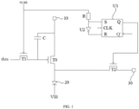
FIG. 1 is a circuit diagram of a pixel driving circuit according to a first embodiment of the present application. -
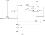
FIG. 2 is a circuit diagram of the pixel driving circuit inFIG. 1 provided with a third response switch according to the present application. -
FIG. 3 shows another connection mode of the third response switch in the pixel driving circuit ofFIG. 2 according to the present application. -
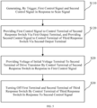
FIG. 4 is a flow chart of a driving method of the pixel driving circuit according to a second embodiment of the present application. -
FIG. 5 is a flow chart of step S30 of the driving method of the pixel driving circuit according to the present application. -
FIG. 6 is a structural schematic diagram of a display panel according to a third embodiment of the present application. - Although the present application can readily be embodied in different forms of embodiment, however, only some of the specific embodiments are shown in the drawings and will be described in detail in the description, while it is understood that the description is to be regarded as an exemplary illustration of the principles of the present application and is not intended to limit the present application to those described herein.
- Thus, one feature pointed out in the description is intended to illustrate one of the features of one embodiment of the present application and is not intended to imply that each embodiment of the present application must have the illustrated feature. In addition, it should be noted that many features are described in the description. Although certain features may be combined to illustrate a possible system design, these features may also be used for other unspecified combinations. Therefore, unless otherwise stated, the illustrated combinations are not intended to be limiting.
- In the embodiments illustrated in the drawings, indications of direction (such as up, down, left, right, front and back) are used to explain that the structure and movement of the various elements of the present application are not absolute but relative. These descriptions are appropriate when these elements are in the positions shown in the drawings. If the description of the positions of the element changes, the indications of the directions change accordingly.
- The exemplary embodiments will now be described more fully with reference to the accompanying drawings. However, the example embodiments can be implemented in a variety of forms and should not be construed as being limited to the examples set forth herein. Rather, these embodiments are provided so that the present application will be more comprehensive and complete, and the concept of example embodiments will be fully communicated to those skilled in the art. The accompanying drawings are only schematic illustrations of the present application and are not necessarily drawn to scale. Like reference numerals in the figures denote identical or similar parts and thus repetitive descriptions thereof will be omitted.
- The preferred embodiment of the present application is further elaborated below in conjunction with the accompanying drawings of the description.
- Referring to
FIG. 1 , the present application provides a pixel driving circuit in which alight emitting unit 20 is provided. Under the display principle, thelight emitting unit 20 may be an AMOLED (Active Matrix Organic Light Emitting Diode) or an LCD (Liquid Crystal Display). In the fabrication of pixel driving circuit, the pixel driving circuit may be fabricated by Amorphous Silicon (A-Si), indium tin oxide (IGZO), Low Temperature Poly-Silicon (LTPS) and so on. - The pixel driving circuit comprises a driving transistor T0 and a storage capacitor C. The first terminal of the driving transistor T0 is connected to a
power source 10, the second terminal is connected to thelight emitting unit 20, the control terminal is connected to the first terminal of the storage capacitor C, and the second terminal of the storage capacitor C is connected to thepower source 10. Thepower source 10 is configured to supply power for lighting thelight emitting unit 20. The storage capacitor C includes two electrode plates, i.e., a first electrode plate and a second electrode plate, the first electrode plate and the second electrode plate are arranged opposite each other, the first electrode plate can be understood as the first terminal, and the second electrode plate can be understood as the second terminal. - The pixel driving circuit further comprises a first response switch T1. The first response switch T1 is provided with a first terminal connected to a data line Data, a control terminal connected to a scan line Scan, and a second terminal connected to the first terminal of the storage capacitor C, the control terminal is configured to respond scan signal provided by the scan line Scan, so as to provide a data signal provided by the data line Data to the first terminal of the storage capacitor C.
- When the
light emitting unit 20 is driven to be lightened, the scan line Scan transmits the scan signal to the first response switch T1. After the control terminal of the first response switch T1 receives the scan signal, the first terminal and the second terminal of the first response switch T1 are turned on, and the data line Data provides a data signal to the first response switch T1. When the first terminal and the second terminal of the first response switch T1 are turned on, the data signal is provided to the first terminal of the storage capacitor C through the first response switch T1, and the data signal can directly enable the storage capacitor C to be charged, thereby affecting the voltage stored in the storage capacitor C, and further controlling the on or off of the driving transistor T0. - The storage capacitor C is configured to be prestored a voltage, and the voltage which is prestored can be associated with the threshold voltage of the driving transistor T0, so that when the
light emitting unit 20 is lightened, the storage voltage stored in the storage capacitor C and the threshold voltage of the driving transistor T0 can cancel each other, so as to avoid the threshold voltage of the driving transistor T0 affecting the lighting of thelight emitting unit 20. For example, the storage capacitor C is charged in advance through thepower source 10 or the data line data until the drive transistor T0 is turned on, and then the charging process for the storage capacitor C is closed. The storage capacitor C starts to discharge continuously, and the capacity gradually decreases. If the capacity stored in the storage capacitor C just meets the shutdown of the driving transistor T0, the voltage stored in the storage capacitor C may be equal to the threshold voltage of the driving transistor T0. - The pixel driving circuit further includes a trigger U1 and a second response switch T2. An input terminal of the trigger U1 is connected to a scan line Scan, and the trigger U1 generates a first control signal in response to a scan signal of the scan line Scan. The first terminal of the second response switch T2 is connected to the second terminal of the driving transistor T0, the second terminal of the second response switch T2 is connected to the
initial voltage terminal 30, the control terminal of the second response switch T2 is connected to the output terminal of the trigger U1, and the control terminal of the second response switch T2 provides the voltage at theinitial voltage terminal 30 to the second terminal of the driving transistor T0 in response to the first control signal. The voltage of theinitial voltage terminal 30 is lower than a threshold voltage of thelight emitting unit 20. - In the technical solution of the embodiment, the scan line Scan provides a scan signal, the control terminal of the first response switch T1 responds to the scan signal, the first terminal and the second terminal of the first response switch T1 are turned on, and the data signal provided by the data line Data is provided to the first terminal of the storage capacitor through the first response switch T1. The second terminal of the storage capacitor C is connected to the
power source 10, and under the joint action of the voltage of thepower source 10 and the voltage of the data signal, the driving transistor T0 is turned on. In this way, the voltage at thepower source 10 can be output to thelight emitting unit 20 through the driving transistor T0 to ensure that thelight emitting unit 20 is lightened. The trigger U1 generates a first control signal upon receiving the scan signal at the input terminal, and the first control signal is transmitted to the second response switch T2. The control terminal of the second response switch T2 responds to the first control signal to turn on the first and second terminals of the second response switch T2. Thus, the voltage at theinitial voltage terminal 30 is provided to the second terminal of the driving transistor through the second response switch T2. The voltage initialization of the second terminal of the driving transistor T0 is completed, which reduces the coupling capacitance or even eliminates the existence of the coupling capacitance, thereby reducing the delayed luminescence of thelight emitting unit 20 and improving the response speed of thewhole display panel 40. - The arrangement of the trigger U1 achieves the voltage initialization of the driving transistor T0 without adding an additional circuit. By using the existing scan line Scan, the trigger U1 receives the scan signal of the scan line Scan to generate a first control signal, and the
initial voltage terminal 30 is controlled by the first control signal. That is, one scan line Scan can control the turning on of the first response switch T1 and can also synchronously control the turning on of the second response switch T2. - The input terminal of the trigger U1 comprises a first input terminal and a second input terminal, the first input terminal and the second input terminal are both connected to the scan line Scan. The pixel driving circuit further includes an inverter U2, one terminal of the inverter U2 is connected to the second input terminal, and another terminal of which is connected to the scan line Scan. The signal flowing to the second input terminal will first pass through the inverter, and the inverter U2 is used to invert the phase of the scan signal by 180 degrees. This ensures that the signals received by the first input terminal and the second input terminal are different, thus ensuring the smooth operation of the trigger U1. For example, if the signal received at the first input terminal is 0, the signal received at the second input terminal is 1. On the contrary, if the signal received at the first input terminal is 1, the signal received at the second input terminal is 0.
- In order to prevent the signal voltage received by the trigger U1 from being too large, the pixel driving circuit further comprises a current limiting resistor R, one terminal of the current limiting resistor R is connected to the scan line Scan, and another terminal thereof is respectively connected to the inverter U2 and the first input terminal. That is to say, before the scan signal flows to the first input terminal and the second input terminal of the trigger U1, the scan signal passes through the current limiting resistor R, and through the sharing of the current limiting resistor R, the current values of the first input terminal and the second input terminal are reduced, and the breakdown of the trigger U1 caused by excessive current is avoided.
- In the related art, the
light emitting unit 20 is susceptible to the external environment, resulting in the brightness of thelight emitting unit 20 being inconsistent and even having a flicker condition after shutdown. - Referring to
FIG. 2 , for this purpose, the pixel driving circuit further includes a third response switch T3, the first terminal of the third response switch T3 is connected to the first terminal of the second response switch T2, and the second terminal of the third response switch T3 is connected to thelight emitting unit 20. - The output terminal of the trigger U1 comprises a first output terminal for providing a first control signal and a second output terminal for providing a second control signal. The second output terminal is connected to a control terminal of the third response switch T3, and the control terminal of the third response switch T3 responds to the second control signal to turn on the first and second terminals of the third response switch T3.
- The first control signal and the second control signal are both generated on the basis of the scan signal. The first control signal comes from the first output terminal and the second control signal comes from the second output terminal. The signals of the first output terminal and the second output terminal are different. If the first control signal is a low level signal, the second control signal is a high level signal. If the first control signal is a high level signal, the second control signal is a low level signal.
- Thus, when initializing the driving transistor T0, the first control signal is at a low level, the control terminal of the second response switch T2 responds to the first control signal at the low level, the first terminal and the second terminal of the second response switch T2 are turned on, and the voltage of the
initial voltage terminal 30 is output to the second terminal of the driving transistor T0, thereby completing the initialization of the driving transistor T0. - Meanwhile, when the second control signal is at a high level, the control terminal of the third response switch T3 is turned off based on the second control signal at a high level, and the first terminal and the second terminal of the third response switch T3 are turned off. An anode of the
light emitting unit 20 is disconnected from the driving transistor T0, and thelight emitting unit 20 is not affected by the external environment. Any of theinitial voltage terminal 30, thepower source 10 and the storage capacitor C is disconnected from thelight emitting unit 20. In this way, none of the voltage of theinitial voltage terminal 30, the voltage of thepower source 10 and the voltage stored in the storage capacitor C can be applied to thelight emitting unit 20, thus ensuring that thelight emitting unit 20 presents a unified black display at this time and avoiding the situation of flashing screen. - Therefore, in the technical solution, the data signal transmission can be completed through the scan line Scan matched with the trigger U1, and the initialization of the driving transistor T0 can be completed by controlling the second response switch T2, and the
light emitting unit 20 is disconnected from the external environment by controlling the third response switch T3, so as to ensure that thelight emitting unit 20 presents a uniform black display when it does not need to emit light. That is, one scan line can control the on and off of three response switches, which simplifies the circuit design. - Further, the trigger U1 is an SR (Set-and-Reset) trigger U1, the first input terminal is an S input terminal, the second input terminal is an R input terminal, the first output terminal is a Q output terminal, and the second output terminal is a Q' output terminal.
- In this embodiment, the inverter U2 is provided so that the signals received at the first input terminal and the second input terminal are reversed. For example, if the S input terminal receives a 0 signal denoting a low level, the R input terminal receives a 1 signal, and the Q output terminal is at a low level, that is, the first control signal is at a low level. In response to the low level of the Q output terminal, the control terminal of the second response switch T2 turned on the first terminal and the second terminal. The Q' output terminal outputs a high level signal, i.e., the second control signal is at a high level, the control terminal of the third response switch T3 turns off the first terminal and the second terminal in response to the high level signal output by the Q' output terminal. The SR trigger is also provided with a clock signal terminal CLK, and the clock signal terminal CLK is used for receiving a clock pulse signal and controlling the turning on of the SR trigger.
- It should be emphasized that the present application can control the turn-on time of the SR trigger through the clock pulse signal, so as to flexibly control the turn-on time of the second response switch T2. This avoids the situation where after the storage capacitor C is charged, the driving transistor T0 is turned on, which affects the initialization of the anode of the
light emitting unit 20. - In addition, the arrangement of the SR trigger can make ensure that the low level signal output at the Q output terminal is applicable to the second response switch T2. Typically, the gate driving voltage required for turning on the second response switch T2 is smaller than the gate driving voltage of the first response switch T1, thereby less control circuits and reducing costs.
- In order to ensure that the response switch effectively responds to the corresponding control signal, the drive transistor T0, the first response switch T1, the second response switch T2 and the third response switch T3 are all P-type transistors. That is to say, the first response switch T1, the second response switch T2 and the third response switch T3 are of the same model, i.e., they are all P-type field-effect transistors (FETs). After receiving the low-level signal, the control terminal of the P-type FET tunes on the first terminal and the second terminal. After receiving the high-level signal, the control terminal of the P-type FET turns off the first terminal and the second terminal.
- The first terminal of the response switch is understood as a source, and the second terminal is understood as a drain. Of course, the first terminal of the response switch can also be understood as a drain, and the second terminal can also be understood as a source. The control terminals of the response switches are grid.
- The first control signal is a low level signal, and the second control signal is a high level signal. The first and second terminals of the second response switch T2 are controlled to be turned on by a low level signal of the first control signal, and the first and second terminals of the third response switch T3 are controlled to be turned off by a high level signal of the second control signal.
- Of course, the first and second response switches T1 and T2 and the third response switch T3 may also be N-type FET. The N-type FET responses to the high level signal, the control terminal of the N-type FET receives the high level signal, and the first and second terminals of the N-type FET are turned on. The control terminal of the N-type FET receives a low level signal, the first and second terminals of the N-type FET are turned off.
- Referring to
FIG. 3 , the driving transistor T0 and the first response switch T1 may be provided as P-type FET, and the second response switch T2 and the third response switch T3 may be provided as N-type FETs. At this time, the control terminal of the second response switch T2 is connected to the second output terminal, that is, the Q' output terminal. The high level of the second control signal is output to the control terminal of the second response switch T2, the first terminal and the second terminal of the second response switch T2 are turned on, and the voltage of the second terminal of the drive transistor T0 is initialized. - The control terminal of the third response switch T3 is connected to the first output terminal, that is, the Q output terminal. The low level of the first control signal is output to the control terminal of the third response switch T3, and the first and second terminals of the third response switch T3 are turned off, so that the
light emitting unit 20 is disconnected from the external environment. - Referring to
FIG. 4 , the present application also provides a driving method of a pixel driving circuit. The pixel driving circuit comprises a driving transistor T0 and a storage capacitor C, a trigger U1, a first response switch T1 and a second response switch T2. A first terminal of the driving transistor T0 is connected to apower source 10, a second terminal of the driving transistor is connected to alight emitting unit 20, a control terminal of the driving transistor is connected to the first terminal of the storage capacitor C, and a second terminal of the storage capacitor C is connected to thepower source 10. - A first terminal of the first response switch T1 is connected to a data line Data, a control terminal of the first response switch T1 is connected to a scan line Scan, a second terminal of the first response switch is connected to the first terminal of the storage capacitor C, an input terminal of the trigger U1 is connected to the scan line Scan, a first terminal of the second response switch T2 is connected to the second terminal of the driving transistor T0, a second terminal of the second response switch T2 is connected to an
initial voltage terminal 30, and a control terminal of the second response switch T2 is connected to an output terminal of the trigger U1. - The driving method of the pixel driving circuit comprises:
- Step S10, controlling the scan line Scan to provide a scan signal, the trigger U1 receiving the scan signal at the input terminal thereof, and generating a first control signal in response to the scan signal; and
- Step S20, providing a voltage of the
initial voltage terminal 30 to the second terminal of the drive transistor T0 by the control terminal of the second response switch T2 in response to the first control signal. - The control terminal of the first response switch T1 responds to the scan signal provided by the scan line Scan, the first terminal and the second terminal of the first response switch T1 are turned on, and the data signal provided by the data line Data is supplied to the first terminal of the storage capacitor C through the first response switch T1. The second terminal of the storage capacitor C is connected to the
power source 10, and under the joint action of the voltage of thepower source 10 and the voltage of the data signal, the driving transistor T0 is turned on. In this way, the voltage at thepower source 10 can be output to thelight emitting unit 20 through the driving transistor T0 to ensure that thelight emitting unit 20 is lightened. The trigger U1 generates a first control signal upon receiving the scan signal at the input terminal, and the first control signal is transmitted to the second response switch T2. The control terminal of the second response switch T2 responds to the first control signal to turn on the first and second terminals of the second response switch T2. Thus, the voltage at theinitial voltage terminal 30 is provided to the second terminal of the driving transistor through the second response switch T2. The voltage initialization of the second terminal of the driving transistor T0 is completed, which reduces the coupling capacitance or even eliminates the existence of the coupling capacitance, thereby reducing the delayed luminescence of thelight emitting unit 20 and improving the response speed of thewhole display panel 40. - Referring to
FIG. 5 , the pixel driving circuit further comprises a third response switch T3, the first terminal of the third response switch T3 is connected to the first terminal of second response switch T2, and a second terminal of third response switch T3 is connected to emittingunit 20; the output terminal of the trigger U1 comprises a first output terminal and a second output terminal, the first output terminal is connected to the control terminal of the second response switch T2, and the second output terminal is connected to a control terminal of the third response switch T3. - The step of generating a first control signal by the trigger U1 in response to the scan signal comprises:
- Step S110, generating, by the trigger U1, the first control signal and a second control signal in response to the scan signal; and
-
Step S 120, providing the first control signal to the control terminal of the second response switch T2 via the first output terminal, and providing the second control signal to the control terminal of the third response switch T3 via the second output terminal. - Following the step of generating a first control signal by the trigger U1 in response to the scan signal, the method comprises:
Step S30, turning off the first terminal and second terminal of the third response switch T3 by the control terminal of the third response switch T3 in response to the second control signal. - The driving transistor T0, the first response switch T1, the second response switch T2 and the third response switch T3 are all P-type field effect transistors. Thus, when initializing the driving transistor T0, the first control signal is at a low level, the control terminal of the second response switch T2 responds to the first control signal at the low level, the first terminal and the second terminal of the second response switch T2 are turned on, and the voltage of the
initial voltage terminal 30 is output to the second terminal of the driving transistor T0, thereby completing the initialization of the driving transistor T0. - Meanwhile, when the second control signal is at a high level, the control terminal of the third response switch T3 is turned off based on the second control signal at a high level, and the first terminal and the second terminal of the third response switch T3 are turned off. An anode of the
light emitting unit 20 is disconnected from the driving transistor T0, and thelight emitting unit 20 is not affected by the external environment. Any one of theinitial voltage terminal 30, thepower source 10 and the storage capacitor C is disconnected from thelight emitting unit 20. In this way, none of the voltage of theinitial voltage terminal 30, the voltage of thepower source 10 and the voltage stored in the storage capacitor C can be applied to thelight emitting unit 20, thus ensuring that thelight emitting unit 20 presents a unified black display at this time and avoiding the situation of flashing screen. - Referring to
FIG. 6 , the present application also provides adisplay panel 40. Thedisplay panel 40 includes adisplay area 410 and anon-display area 420 surrounding thedisplay area 410. Thedisplay panel 40 comprises a gate driving circuit disposed in thenon-display area 420 and the pixel driving circuit as described above disposed in thedisplay area 410, the gate driving circuit is connected to the pixel driving circuit, and the gate driving circuit is configured to provide a scan signal to the pixel driving circuit. The gate driving circuit is disposed in thenon-display area 420 so that interference to the display screen can be avoided. - The pixel driving circuit comprises a driving transistor T0 and a storage capacitor C. The first terminal of the driving transistor T0 is connected to a
power source 10, the second terminal is connected to thelight emitting unit 20, the control terminal is connected to the first terminal of the storage capacitor C, and the second terminal of the storage capacitor C is connected to thepower source 10. Thepower source 10 is used for supplying power for lighting thelight emitting unit 20. The storage capacitor C includes two electrode plates, i.e., a first electrode plate and a second electrode plate, the first electrode plate and the second electrode plate are arranged opposite each other, the first electrode plate can be understood as the first terminal, and the second electrode plate can be understood as the second terminal. - The pixel driving circuit further comprises a first response switch T1. The first response switch T1 is provided with a first terminal connected to a data line Data, a control terminal connected to a scan line Scan, and a second terminal connected to the first terminal of the storage capacitor C, the control terminal is configured to respond scan signal provided by the scan line Scan, so as to provide a data signal provided by the data line Data to the first terminal of the storage capacitor C.
- When the driving
light emitting unit 20 is lightened, the scan line Scan transmits the scan signal to the first response switch T1. After the control terminal of the first response switch T1 receives the scan signal, the first terminal and the second terminal of the first response switch T1 are turned on, and the data line Data provides a data signal to the first response switch T1. When the first terminal and the second terminal of the first response switch T1 are turned on, the data signal is provided to the first terminal of the storage capacitor C through the first response switch T1, and the data signal can directly enable the storage capacitor C to be charged, thereby affecting the voltage stored in the storage capacitor C, and further controlling the on or off of the driving transistor T0. - The storage capacitor C is configured to be prestored a voltage, and the voltage which is prestored can be associated with the threshold voltage of the driving transistor T0, so that when the
light emitting unit 20 is lightened, the storage voltage stored in the storage capacitor C and the threshold voltage of the driving transistor T0 can cancel each other, so as to avoid the threshold voltage of the driving transistor T0 affecting the lighting of thelight emitting unit 20. For example, the storage capacitor C is charged in advance through thepower source 10 or the data line data until the drive transistor T0 is turned on, and then the charging process for the storage capacitor C is closed. The storage capacitor C starts to discharge continuously, and the capacity gradually decreases. If the capacity stored in the storage capacitor C just meets the shutdown of the driving transistor T0, the voltage stored in the storage capacitor C can be equal to the threshold voltage of the driving transistor T0. - The pixel driving circuit further includes a trigger U1 and a second response switch T2. An input terminal of the trigger U1 is connected to a scan line Scan, and the trigger U1 generates a first control signal in response to a scan signal of the scan line Scan. The first terminal of the second response switch T2 is connected to the second terminal of the driving transistor T0, the second terminal of the second response switch T2 is connected to the
initial voltage terminal 30, the control terminal of the second response switch T2 is connected to the output terminal of the trigger U1, and the control terminal of the second response switch T2 provides the voltage at theinitial voltage terminal 30 to the second terminal of the driving transistor T0 in response to the first control signal. The voltage of theinitial voltage terminal 30 is lower than a threshold voltage of thelight emitting unit 20. - In the technical solution of the embodiment, the scan line Scan provides a scan signal, the control terminal of the first response switch T1 responds C to the scan signal, the first terminal and the second terminal of the first response switch T1 are turned on, and the data signal provided by the data line Data is provided to the first terminal of the storage capacitor through the first response switch T1. The second terminal of the storage capacitor C is connected to the
power source 10, and under the joint action of the voltage of thepower source 10 and the voltage of the data signal, the driving transistor T0 is turned on. In this way, the voltage at thepower source 10 can be output to thelight emitting unit 20 through the driving transistor T0 to ensure that thelight emitting unit 20 is lightened. The trigger U1 generates a first control signal upon receiving the scan signal at the input terminal, and the first control signal is transmitted to the second response switch T2. The control terminal of the second response switch T2 responds to the first control signal to turn on the first and second terminals of the second response switch T2. Thus, the voltage at theinitial voltage terminal 30 is provided to the second terminal of the driving transistor through the second response switch T2. The voltage initialization of the second terminal of the driving transistor T0 is completed, which reduces the coupling capacitance or even eliminates the existence of the coupling capacitance, thereby reducing the delayed luminescence of thelight emitting unit 20 and improving the response speed of thewhole display panel 40. - In addition, in this embodiment, the pixel driving circuit may be integrally provided in the
display area 410 or partially provided in thenon-display area 420. For example, thelight emitting unit 20 is provided in thedisplay area 410 and components other than thelight emitting unit 20 are provided in thenon-display area 420. - While the present application has been described with reference to several exemplary embodiments, it should be understood that the terms used are illustrative and exemplary and are not limiting. Since the present application can be embodied in various forms without departing from the spirit or essence of the present application, it should therefore be understood that the foregoing embodiments are not limited to any of the foregoing details, but are to be interpreted broadly within the spirit and scope defined by the appended claims, so that all variations and modifications falling within the scope of the claims or their equivalents are to be covered by the appended claims.
Claims (20)
- A pixel driving circuit comprising:a driving transistor, a first terminal of the driving transistor being connected to a power source, a second terminal of the driving transistor being connected to a light emitting unit;a storage capacitor, a first terminal of the storage capacitor being connected to a control terminal of the driving transistor, and a second terminal of the storage capacitor being connected to the power source;a first response switch, provided with a first terminal connected to a data line, a control terminal connected to a scan line, and a second terminal connected to the first terminal of the storage capacitor, the control terminal being configured to respond to a scan signal provided by the scan line to provide a data signal provided by the data line to the first terminal of the storage capacitor; anda trigger with an input terminal connected to the scan line, and the trigger generating a first control signal in response to the scan signal of the scan line; anda second response switch with a first terminal connected to the second terminal of the driving transistor, a second terminal connected to an initial voltage terminal, a control terminal connected to an output terminal of the trigger, wherein the control terminal of the second response switch provides a voltage of the initial voltage terminal to the second terminal of the driving transistor in response to the first control signal.
- The pixel driving circuit according to claim 1, wherein the input terminal of the trigger comprises a first input terminal and a second input terminal, and the first input terminal and the second input terminal being connected to the scan line; and
wherein the pixel driving circuit further comprises an inverter, one terminal of the inverter being connected to the second input terminal, and another terminal of the inverter being connected to the scan line. - The pixel driving circuit according to claim 2, wherein the pixel driving circuit further comprises a current limiting resistor, one terminal of the current limiting resistor being connected to the scan line, and another terminal of the current limiting resistor being connected to the inverter and the first input terminal.
- The pixel driving circuit according to claim 2, wherein the pixel driving circuit further comprises a third response switch, a first terminal of the third response switch being connected to the first terminal of the second response switch, and a second terminal of the third response switch being connected to the light emitting unit; and
wherein the output terminal of the trigger comprises a first output terminal for providing the first control signal and a second output terminal for providing a second control signal, the second output terminal being connected to a control terminal of the third response switch, the control terminal of the third response switch turning on the first terminal and the second terminal of the third response switch in response to the second control signal. - The pixel driving circuit according to claim 4, wherein the trigger is an SR trigger, the first input terminal is an S input terminal, the second input terminal is an R input terminal, the first output terminal is a Q output terminal, and the second output terminal is a Q' output terminal.
- The pixel driving circuit according to claim 4, wherein the first response switch, the second response switch and the third response switch are P-type tubes.
- The pixel driving circuit according to claim 6, wherein the first control signal is a low level signal, and the second control signal is a high level signal.
- The pixel driving circuit according to claim 1, wherein a gate driving voltage required for turning on the second response switch is smaller than a gate driving voltage of the first response switch.
- The pixel driving circuit according to claim 1, wherein the voltage of the initial voltage terminal is lower than a threshold voltage of the light emitting unit.
- A driving method of a pixel driving circuit, wherein the pixel driving circuit comprises a driving transistor, a storage capacitor, a trigger, a first response switch and a second response switch, wherein a first terminal of the driving transistor is connected to a power source, a second terminal of the driving transistor is connected to a light emitting unit, a control terminal of the driving transistor is connected to a first terminal of the storage capacitor, and a second terminal of the storage capacitor is connected to the power source;a first terminal of the first response switch is connected to a data line, a control terminal of the first response switch is connected to a scan line, a second terminal of the first response switch is connected to the first terminal of the storage capacitor, an input terminal of the trigger is connected to the scan line, a first terminal of the second response switch is connected to the second terminal of the driving transistor, a second terminal of the second response switch is connected to an initial voltage terminal, and a control terminal of the second response switch is connected to an output terminal of the trigger;wherein the driving method of the pixel driving circuit comprises:controlling the scan line to provide a scan signal, the trigger receiving the scan signal at the input terminal thereof, and the trigger generating a first control signal in response to the scan signal; andproviding a voltage of the initial voltage terminal to the second terminal of the drive transistor by the control terminal of the second response switch in response to the first control signal.
- The driving method of the pixel driving circuit according to claim 10, wherein the pixel driving circuit further comprises a third response switch, a first terminal of the third response switch being connected to the first terminal of the second response switch, and a second terminal of the third response switch being connected to the light emitting unit; and wherein the output terminal of the trigger comprises a first output terminal and a second output terminal, the first output terminal being connected to the control terminal of the second response switch, and the second output terminal being connected to a control terminal of the third response switch;
wherein the step of generating a first control signal by the trigger in response to the scan signal comprises:generating, by the trigger, the first control signal and a second control signal in response to the scan signal; andproviding the first control signal to the control terminal of the second response switch via the first output terminal, and providing the second control signal to the control terminal of the third response switch via the second output terminal. - The driving method of the pixel driving circuit according to claim 11, wherein after the step of generating, by the trigger, a first control signal in response to the scan signal, the method comprises:
turning off the first terminal and second terminal of the third response switch by the control terminal of the third response switch in response to the second control signal. - A display panel comprising a display area and a non-display area surrounding the display area, wherein the display panel comprises a gate driving circuit disposed in the non-display area and a pixel driving circuit disposed in the display area, the gate driving circuit being connected to the pixel driving circuit, and the gate driving circuit being configured for providing a scan signal to the pixel driving circuit;
wherein the pixel driving circuit comprises:a driving transistor, a first terminal of the driving transistor being connected to a power source, a second terminal of the driving transistor being connected to a light emitting unit;a storage capacitor, a first terminal of the storage capacitor being connected to a control terminal of the driving transistor, and a second terminal of the storage capacitor being connected to the power source;a first response switch, provided with a first terminal connected to a data line, a control terminal connected to a scan line, and a second terminal connected to the first terminal of the storage capacitor, the control terminal being configured to respond to a scan signal provided by the scan line to provide a data signal provided by the data line to the first terminal of the storage capacitor; anda trigger with an input terminal connected to the scan line, and the trigger generating a first control signal in response to the scan signal of the scan line; anda second response switch with a first terminal connected to the second terminal of the driving transistor, a second terminal connected to an initial voltage terminal, a control terminal connected to an output terminal of the trigger, wherein the control terminal of the second response switch provides a voltage of the initial voltage terminal to the second terminal of the driving transistor in response to the first control signal. - The display panel according to claim 13, wherein the input terminal of the trigger comprises a first input terminal and a second input terminal, and the first input terminal and the second input terminal being connected to the scan line; and
wherein the pixel driving circuit further comprises an inverter, one terminal of the inverter being connected to the second input terminal, and another terminal of the inverter being connected to the scan line. - The display panel according to claim 14, wherein the pixel driving circuit further comprises a current limiting resistor, one terminal of the current limiting resistor being connected to the scan line, and another terminal of the current limiting resistor being connected to the inverter and the first input terminal.
- The display panel according to claim 14, wherein the pixel driving circuit further comprises a third response switch, a first terminal of the third response switch being connected to the first terminal of the second response switch, and a second terminal of the third response switch being connected to the light emitting unit; and
wherein the output terminal of the trigger comprises a first output terminal for providing the first control signal and a second output terminal for providing a second control signal, the second output terminal being connected to a control terminal of the third response switch, the control terminal of the third response switch turning on the first terminal and the second terminal of the third response switch in response to the second control signal. - The display panel according to claim 16, wherein the trigger is an SR trigger, the first input terminal is an S input terminal, the second input terminal is an R input terminal, the first output terminal is a Q output terminal, and the second output terminal is a Q' output terminal.
- The display panel according to claim 16, wherein the first response switch, the second response switch and the third response switch are P-type tubes.
- The display panel according to claim 18, wherein the first control signal is a low level signal, and the second control signal is a high level signal.
- The display panel according to claim 10, wherein a gate driving voltage required for turning on the second response switch is smaller than a gate driving voltage of the first response switch.
Applications Claiming Priority (2)
| Application Number | Priority Date | Filing Date | Title |
|---|---|---|---|
| CN202211244269.5A CN115312001B (en) | 2022-10-12 | 2022-10-12 | Pixel driving circuit, driving method thereof, and display device |
| PCT/CN2023/095574 WO2024077961A1 (en) | 2022-10-12 | 2023-05-22 | Pixel driving circuit and driving method therefor, and display apparatus |
Publications (3)
| Publication Number | Publication Date |
|---|---|
| EP4418251A1 true EP4418251A1 (en) | 2024-08-21 |
| EP4418251A4 EP4418251A4 (en) | 2024-10-16 |
| EP4418251B1 EP4418251B1 (en) | 2025-12-03 |
Family
ID=83868227
Family Applications (1)
| Application Number | Title | Priority Date | Filing Date |
|---|---|---|---|
| EP23876172.0A Active EP4418251B1 (en) | 2022-10-12 | 2023-05-22 | Pixel driving circuit and driving method therefor, and display apparatus |
Country Status (6)
| Country | Link |
|---|---|
| US (1) | US11942039B1 (en) |
| EP (1) | EP4418251B1 (en) |
| JP (1) | JP7675941B2 (en) |
| KR (1) | KR20250057911A (en) |
| CN (1) | CN115312001B (en) |
| WO (1) | WO2024077961A1 (en) |
Families Citing this family (2)
| Publication number | Priority date | Publication date | Assignee | Title |
|---|---|---|---|---|
| CN115312001B (en) * | 2022-10-12 | 2022-12-09 | 惠科股份有限公司 | Pixel driving circuit, driving method thereof, and display device |
| CN115953985B (en) * | 2022-12-28 | 2023-11-17 | 惠科股份有限公司 | Pixel unit, display panel and display device |
Family Cites Families (21)
| Publication number | Priority date | Publication date | Assignee | Title |
|---|---|---|---|---|
| JP2003108055A (en) | 2001-09-28 | 2003-04-11 | Toshiba Corp | Display device |
| US8760374B2 (en) * | 2004-05-21 | 2014-06-24 | Semiconductor Energy Laboratory Co., Ltd. | Display device having a light emitting element |
| US7397448B2 (en) * | 2004-07-16 | 2008-07-08 | E.I. Du Pont De Nemours And Company | Circuits including parallel conduction paths and methods of operating an electronic device including parallel conduction paths |
| KR100624137B1 (en) * | 2005-08-22 | 2006-09-13 | 삼성에스디아이 주식회사 | Pixel circuit of organic electroluminescent display and driving method thereof |
| JP2008083680A (en) * | 2006-08-17 | 2008-04-10 | Seiko Epson Corp | Electro-optical device and electronic apparatus |
| KR101429711B1 (en) * | 2007-11-06 | 2014-08-13 | 삼성디스플레이 주식회사 | OLED display and driving method thereof |
| KR102424978B1 (en) * | 2015-02-26 | 2022-07-26 | 삼성디스플레이 주식회사 | Organic light emitting display |
| CN104751799B (en) * | 2015-04-10 | 2016-12-14 | 京东方科技集团股份有限公司 | Image element circuit and driving method, display device |
| CN108389548B (en) * | 2018-03-16 | 2020-03-20 | 京东方科技集团股份有限公司 | Pixel circuit, driving method thereof and display panel |
| CN111402782B (en) | 2018-12-14 | 2021-09-03 | 成都辰显光电有限公司 | Digital driving pixel circuit and method for digitally driving pixel |
| KR102765728B1 (en) | 2019-08-02 | 2025-02-13 | 삼성디스플레이 주식회사 | Pixel and display device having the same |
| KR102740895B1 (en) * | 2019-10-16 | 2024-12-12 | 엘지디스플레이 주식회사 | Scan Driver and Display Device including the Scan Driver |
| KR102795160B1 (en) * | 2019-12-31 | 2025-04-15 | 엘지디스플레이 주식회사 | Emission Driver and Organic Light Emitting Diode Display Device Including The Same |
| DE102020204708A1 (en) * | 2020-04-14 | 2021-10-14 | OSRAM Opto Semiconductors Gesellschaft mit beschränkter Haftung | PICTURE ELEMENT AND METHOD OF OPERATING A PICTURE ELEMENT |
| CN114093319A (en) * | 2021-11-26 | 2022-02-25 | 长沙惠科光电有限公司 | Pixel compensation circuit, pixel driving method and display device |
| KR20230102885A (en) * | 2021-12-30 | 2023-07-07 | 엘지디스플레이 주식회사 | Light Emitting Display Device and Driving Method of the same |
| CN114822396B (en) * | 2022-05-12 | 2023-01-10 | 惠科股份有限公司 | Pixel driving circuit and display panel |
| CN114743501B (en) * | 2022-06-09 | 2022-08-23 | 惠科股份有限公司 | Compensation circuit, control chip and display device |
| CN115171590A (en) * | 2022-07-28 | 2022-10-11 | 惠科股份有限公司 | Pixel driving circuit and display panel |
| CN115019729B (en) * | 2022-08-04 | 2022-11-25 | 惠科股份有限公司 | Pixel driving circuit, display panel and control method thereof |
| CN115312001B (en) * | 2022-10-12 | 2022-12-09 | 惠科股份有限公司 | Pixel driving circuit, driving method thereof, and display device |
-
2022
- 2022-10-12 CN CN202211244269.5A patent/CN115312001B/en active Active
-
2023
- 2023-05-22 KR KR1020257011569A patent/KR20250057911A/en active Pending
- 2023-05-22 WO PCT/CN2023/095574 patent/WO2024077961A1/en not_active Ceased
- 2023-05-22 JP JP2024538714A patent/JP7675941B2/en active Active
- 2023-05-22 EP EP23876172.0A patent/EP4418251B1/en active Active
- 2023-06-06 US US18/330,273 patent/US11942039B1/en active Active
Also Published As
| Publication number | Publication date |
|---|---|
| CN115312001B (en) | 2022-12-09 |
| WO2024077961A1 (en) | 2024-04-18 |
| US11942039B1 (en) | 2024-03-26 |
| KR20250057911A (en) | 2025-04-29 |
| US20240127752A1 (en) | 2024-04-18 |
| JP2024545351A (en) | 2024-12-05 |
| CN115312001A (en) | 2022-11-08 |
| EP4418251A4 (en) | 2024-10-16 |
| JP7675941B2 (en) | 2025-05-13 |
| EP4418251B1 (en) | 2025-12-03 |
Similar Documents
| Publication | Publication Date | Title |
|---|---|---|
| US11308907B2 (en) | Shift register and driving method of shift register, gate driving circuit and display panel and device | |
| US9324271B2 (en) | Pixel driver | |
| WO2021203497A1 (en) | Pixel driving circuit and display panel | |
| US11942039B1 (en) | Pixel driving circuit, driving method thereof and display device | |
| CN112233621B (en) | A pixel drive circuit, a display panel and an electronic device | |
| CN103035195A (en) | Light emitting element drive circuit, pixel circuit, display panel and display | |
| CN103035198A (en) | Light-emitting element driving circuit and related pixel circuit and application thereof | |
| EP4386733A1 (en) | Pixel driving circuit, and display panel and control method therefor | |
| US11315515B2 (en) | GOA circuit, display panel, and electronic device | |
| US9978333B2 (en) | Timing sequences generation circuits and liquid crystal devices | |
| CN111383597A (en) | Pixel circuit and full-screen display equipment | |
| CN111402782A (en) | Digital driving pixel circuit and method for digitally driving pixel | |
| US11348540B2 (en) | Display device driving method, and display device | |
| EP4693269A1 (en) | Pixel drive circuit and display panel | |
| US20240021118A1 (en) | Driving circuit and display panel | |
| CN115035861A (en) | Pixel circuit, driving method thereof and display panel | |
| US20240282261A1 (en) | Display panel and display apparatus | |
| US11488525B2 (en) | Display panel driving method of turning on an active switch corresponding to each pixel of the display panel for releasing charges stored in the display panel during operation, and drive circuit implementing the same | |
| US20250061839A1 (en) | Pixel driving circuit, driving method thereof, and display panel | |
| US12094383B2 (en) | Display driver and charge recycling method using the same | |
| CN106898302A (en) | Image element circuit control unit, driving method, image element circuit and display device | |
| US11645984B2 (en) | Display device driving method, and display device | |
| CN114708828B (en) | Pixel circuit and display panel | |
| CN215868588U (en) | Light-emitting drive circuit and display panel | |
| CN115359756A (en) | Detection compensation circuit and display panel |
Legal Events
| Date | Code | Title | Description |
|---|---|---|---|
| STAA | Information on the status of an ep patent application or granted ep patent |
Free format text: STATUS: THE INTERNATIONAL PUBLICATION HAS BEEN MADE |
|
| PUAI | Public reference made under article 153(3) epc to a published international application that has entered the european phase |
Free format text: ORIGINAL CODE: 0009012 |
|
| STAA | Information on the status of an ep patent application or granted ep patent |
Free format text: STATUS: REQUEST FOR EXAMINATION WAS MADE |
|
| 17P | Request for examination filed |
Effective date: 20240516 |
|
| AK | Designated contracting states |
Kind code of ref document: A1 Designated state(s): AL AT BE BG CH CY CZ DE DK EE ES FI FR GB GR HR HU IE IS IT LI LT LU LV MC ME MK MT NL NO PL PT RO RS SE SI SK SM TR |
|
| A4 | Supplementary search report drawn up and despatched |
Effective date: 20240913 |
|
| RIC1 | Information provided on ipc code assigned before grant |
Ipc: G09G 3/3233 20160101ALI20240909BHEP Ipc: G09G 3/3225 20160101AFI20240909BHEP |
|
| GRAP | Despatch of communication of intention to grant a patent |
Free format text: ORIGINAL CODE: EPIDOSNIGR1 |
|
| STAA | Information on the status of an ep patent application or granted ep patent |
Free format text: STATUS: GRANT OF PATENT IS INTENDED |
|
| DAV | Request for validation of the european patent (deleted) | ||
| DAX | Request for extension of the european patent (deleted) | ||
| INTG | Intention to grant announced |
Effective date: 20250624 |
|
| P01 | Opt-out of the competence of the unified patent court (upc) registered |
Free format text: CASE NUMBER: UPC_APP_3311_4418251/2025 Effective date: 20250813 |
|
| GRAS | Grant fee paid |
Free format text: ORIGINAL CODE: EPIDOSNIGR3 |
|
| GRAA | (expected) grant |
Free format text: ORIGINAL CODE: 0009210 |
|
| STAA | Information on the status of an ep patent application or granted ep patent |
Free format text: STATUS: THE PATENT HAS BEEN GRANTED |
|
| AK | Designated contracting states |
Kind code of ref document: B1 Designated state(s): AL AT BE BG CH CY CZ DE DK EE ES FI FR GB GR HR HU IE IS IT LI LT LU LV MC ME MK MT NL NO PL PT RO RS SE SI SK SM TR |
|
| REG | Reference to a national code |
Ref country code: CH Ref legal event code: F10 Free format text: ST27 STATUS EVENT CODE: U-0-0-F10-F00 (AS PROVIDED BY THE NATIONAL OFFICE) Effective date: 20251203 Ref country code: GB Ref legal event code: FG4D |
|
| REG | Reference to a national code |
Ref country code: DE Ref legal event code: R096 Ref document number: 602023009392 Country of ref document: DE |
|
| REG | Reference to a national code |
Ref country code: IE Ref legal event code: FG4D |
|
| REG | Reference to a national code |
Ref country code: NL Ref legal event code: MP Effective date: 20251203 |
|
| PG25 | Lapsed in a contracting state [announced via postgrant information from national office to epo] |
Ref country code: ES Free format text: LAPSE BECAUSE OF FAILURE TO SUBMIT A TRANSLATION OF THE DESCRIPTION OR TO PAY THE FEE WITHIN THE PRESCRIBED TIME-LIMIT Effective date: 20251203 |
|
| REG | Reference to a national code |
Ref country code: LT Ref legal event code: MG9D |
|
| PG25 | Lapsed in a contracting state [announced via postgrant information from national office to epo] |
Ref country code: NO Free format text: LAPSE BECAUSE OF FAILURE TO SUBMIT A TRANSLATION OF THE DESCRIPTION OR TO PAY THE FEE WITHIN THE PRESCRIBED TIME-LIMIT Effective date: 20260303 |
|
| PG25 | Lapsed in a contracting state [announced via postgrant information from national office to epo] |
Ref country code: HR Free format text: LAPSE BECAUSE OF FAILURE TO SUBMIT A TRANSLATION OF THE DESCRIPTION OR TO PAY THE FEE WITHIN THE PRESCRIBED TIME-LIMIT Effective date: 20251203 Ref country code: FI Free format text: LAPSE BECAUSE OF FAILURE TO SUBMIT A TRANSLATION OF THE DESCRIPTION OR TO PAY THE FEE WITHIN THE PRESCRIBED TIME-LIMIT Effective date: 20251203 |
|
| PG25 | Lapsed in a contracting state [announced via postgrant information from national office to epo] |
Ref country code: RS Free format text: LAPSE BECAUSE OF FAILURE TO SUBMIT A TRANSLATION OF THE DESCRIPTION OR TO PAY THE FEE WITHIN THE PRESCRIBED TIME-LIMIT Effective date: 20260303 |
|
| PG25 | Lapsed in a contracting state [announced via postgrant information from national office to epo] |
Ref country code: PL Free format text: LAPSE BECAUSE OF FAILURE TO SUBMIT A TRANSLATION OF THE DESCRIPTION OR TO PAY THE FEE WITHIN THE PRESCRIBED TIME-LIMIT Effective date: 20251203 |
|
| PG25 | Lapsed in a contracting state [announced via postgrant information from national office to epo] |
Ref country code: LV Free format text: LAPSE BECAUSE OF FAILURE TO SUBMIT A TRANSLATION OF THE DESCRIPTION OR TO PAY THE FEE WITHIN THE PRESCRIBED TIME-LIMIT Effective date: 20251203 |
|
| PG25 | Lapsed in a contracting state [announced via postgrant information from national office to epo] |
Ref country code: BG Free format text: LAPSE BECAUSE OF FAILURE TO SUBMIT A TRANSLATION OF THE DESCRIPTION OR TO PAY THE FEE WITHIN THE PRESCRIBED TIME-LIMIT Effective date: 20251203 |